Abstract
A rotational d-q current control scheme based on a Particle Swarm Optimization- Proportional-Integral (PSO-PI) controller, is used to drive an induction motor (IM) through an Ultra Sparse Z-source Matrix Converter (USZSMC). To minimize the overall size of the system, the lowest feasible values of Z-source elements are calculated by considering the both timing and aspects of the circuit. A meta-heuristic method is integrated to the control system in order to find optimal coefficient values in a single multimodal problem. Henceforth, the effect of all coefficients in minimizing the total harmonic distortion (THD) and balancing the stator current are considered simultaneously. Through changing the reference point of magnitude or frequency, the modulation index can be automatically adjusted and respond to changes without heavy computational cost. The focus of this research is on a reliable and lightweight system with low computational resources. The proposed scheme is validated through both simulation and experimental results.
1. Introduction
In traditional converters, a two-stage AC/DC/AC system is used to convert the input AC voltage and current to a variable amplitude and/or a variable frequency. Such instrumentation requires bulky DC-link storage such as electrolytic capacitors [1]. Removing bulky capacitor results in compact converters [1,2], and coupling both sides of the converter to switches results in a high power density for the matrix converter (MC) [3]. Regardless of the load, such a structure also provides reliable input power factor correction by implementing proper modulation [4,5].
The MC family is still categorized as a laboratory AC/DC driver with little reliable potential for industrial use [6,7] because of the control complexity [8], sensitivity in the face of abnormal input [9], limitation of the voltage transfer ratio up to 86.6% [10], and excess semiconductor switches [11]. These are the most critical obstacles to overcome, and, hence, solutions would be welcomed by manufacturers and industrial developers. Furthermore, a direct matrix converter has a flow power path in the bidirectional mode for transmitting the power [10], either from the grid to the load or, it can be reversed in the generative mode. The bidirectional capability is an advantage for various applications [12]; nevertheless, in the aerospace industry, where the power flow must be in one direction, it counts as a drawback [13]. Although eliminating the bulky DC-link is an inherent specification of MCs, the excessive number of switches for the conventional topology increases the weight, which makes it unsuitable for aerospace manufacturing [13,14]. Connecting the MC to an unbalanced grid has an effect on the controlling system, which has been discussed extensively for the MC under abnormal input supply conditions [9].
Unbalanced voltage supply can result in distorting input/output harmonic currents, and consequently, can affect the induction motor (IM) driving. Normally, the IMs are not able to operate under abnormal supply conditions [15]. The unbalanced voltage increases the rotor losses, which results in both rotor and stator temperature rises that can cause serious damage to the three phase IM, such as decreased electromagnetic-torque, and increased heat and vibration. This affects machine insulation life [16]. Several published investigations have reported ways to decrease the unwanted effects of abnormal voltage supplies [9,17]. A feed-forward compensation strategy is presented in [18], which could achieved balanced output currents under abnormal conditions by adapting the voltage modulation index. Furthermore, two modulation methods of input current for the MC are provided in [19], and their input and output performance were also analyzed under the unbalanced input and output conditions.
The computational optimization methods using bio-inspired technologies have been significantly developed in recent years. They can effectively increase the efficiency of systems. References [20,21] studied optimization of switching state, using Crazy- particle swarm optimization and real-time PSOIOC in order to predict the next switching state in, and the output can help control the state of switches in the matrix converter.
This paper proposes a novel driving strategy for an IM fed by an ultra-sparse Z-source MC, which can boost the voltage transfer ratio up to unity by using an X-shape Z-source network with small size components. It functions under unbalanced and distorted input voltage conditions while minimizing the total harmonic distortion (THD) of the output current through the Particle Swarm Optimization-PI (PSO-PI) control scheme. The PI parameters of the feedback/feedforward controller can be tuned by various methods such as Ziegler–Nichols (ZN) but the internal impact of other elements and the PI parameters cannot be simultaneously reflected. In this paper, the THD of the output current has been monitored and the proportional and integral parameters of controllers are optimized in the d-q scheme by using a PSO method while the inter-correlations of the other elements and the PI parameters is considered together. These capacities may make the matrix converter suitable for industries that require high reliability, in particular aerospace manufacturing [11,22].
2. Z-Source and Voltage Transfer Ratio
The Ultra Sparse Matrix Converter (USMC) is a kind of indirect matrix converter (IMC) with a low-complexity modulation scheme compared with the conventional IMC. It only requires nine semiconductor switches—three switches in the rectification part and the remaining six used in the inversion part. This topology could provide all the desired characteristics that a common matrix converter would, except power flow bi-directionality. The Z-source network operates simultaneously as an energy reservoir and a filter to overcome the current and voltage ripple [7], as depicted in Figure 1.
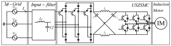
Figure 1.
The ultra-sparse Z-source matrix converter topology.
The indirect energy conversion (such as matrix converter) requires more semiconductor devices than a conventional AC/AC indirect power frequency converter, since no monolithic bi-directional switches exist and consequently, discrete unidirectional devices, variously arranged, have to be used for each bi-directional switch. Finally, it is particularly sensitive to disturbances of the input voltage system.
There is an alternative option of indirect energy conversion by employing IMC or the sparse matrix converter. The (very/ultra) sparse matrix converter is an AC/AC converter which offers a reduced number of components, a low-complexity modulation scheme, and low realization effort. Sparse matrix converters avoid the multi-step computation procedure of the conventional matrix converter, improving system reliability in industrial operations. Their principal application is in highly compact integrated AC drives. The characteristics of the sparse matrix converter are the following:
- (1)
- Quasi-Direct AC/AC conversion with no DC-link energy storage elements.
- (2)
- Sinusoidal input current in phase with mains voltage.
- (3)
- Zero DC-link current commutation scheme resulting in lower modulation complexity and very high reliability.
- (4)
- Low complexity of power circuit/power modules available.
- (5)
- The ultra-sparse matrix converter shows extremely low realization effort, in case unidirectional power flow can be accepted (admissible displacement of 30° the input current fundamental and input voltage, as well as for the output voltage fundamental and output current), accordingly, a possible application area would be variable speed permanent-magnet synchronous motor (PMSM) or IM drives with low dynamics.
As with the DC-link based Voltage Source Inverter (VSI) and Current Source Inverter (CSI) controllers’ separate stages are provided for voltage and current conversion, but the DC-link has no intermediate storage element. Generally, by employing matrix converters, the storage element in the DC-link is eliminated from the cost of a larger number of semiconductors. Matrix converters are often seen as a future concept for variable-speed drive technology, but despite intensive research over the decades, they have until now, only achieved low industrial penetration. However, citing the recent availability of low-cost, high-performance semiconductors, at least one larger drive manufacturer has been actively promoting matrix converters over the past few years.
Moreover, the Z-source converter has two operating modes in this study: DC/AC inversion and AC/DC rectification. Circuit analysis for both operating modes shows that the new topology does not impose critical conflicts in circuit design or extra parameterization restrictions. On the contrary, one version of the proposed zero current (ZC) can take full advantage of Z-source network components in both operating modes, i.e., a pair of Z-source inductor and capacitor can be used as the low-pass filter in AC/DC rectification.
The Z-source Inverter (ZSI) works primarily in two distinctive functioning modes: first across the normal operating mode or non-shoot-through state, where the accumulated power is applied into a corporate output voltage. Supposedly, a steady DC-link voltage delivers the ZSI within a switching period. In Figure 2a, a current source as the output of the Z-source system demonstrates a limited current flow, while Figure 2b under the same input DC voltage is an open circuit. Meanwhile, in Figure 2c the output of the Z-source network is shorted where the high current flows through the circuit, and, simultaneously, the -DC supply for the network is zero. In the shoot-through state, the Z-source network stores the inductive and capacitive power with its elements. The third approach occurs when two switches from the same leg of the inverter are ON.
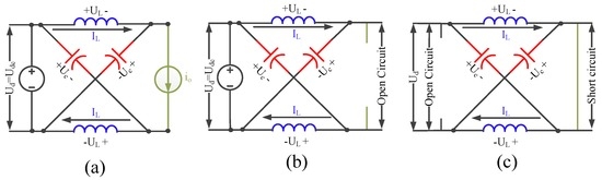
Figure 2.
Z-source network in the mode of (a) dynamic non-shoot-through; (b) inactive non-shoot-through; and (c) shoot-through states.
According to [23], the timing of the shoot-through and non-shoot-through state mode are defined by T0 and T1. If we suppose UL is constant in their interval integration, the current variation in the shoot-through and non-shoot-through mode can be extracted as Equation (1):
On the other hand, the switching period is assumed to be T, where T0 + T1 = T, and, during the switching period in the steady state mode, the average voltage of the inductor is moderated by keeping close to zero; hence, we have:
During the non-shoot-through state, when T1 is greater than or equal to T0, the voltage Ui across the inverter bridges can be expanded:
The time-based boost factor (BFt) is determined in Equation (4). On the other hand, based on the symmetrical properties of the Z-source network, we not only have the same equations for current but also the ratio for the inductive to capacitive current of Z-source has been kept load dependent, as can be seen in Equation (5):
where Z has been assumed to be the equivalent load of the connected IM rear-end Z-source inverter in complex frequency (S-domain). Therefore, with the same strategy for the conjugate properties of voltage, expectations can be extracted by Equation (6):
Hence:
In contrast, the boost factor that is normally defined by Ui/Udc which is independent of the Z-source output and consequently from input grid power and dependent on induction motor elements as shown in Equation (8):
Two approaches are plausible to increase the boost factor ratio. First, by increasing T0 to near T1 based on Equation (4); second, determining L and C values in the way that the poles are drawn to zero based on Equation (8). T0 determine the L and C, Equation (8) should be plotted. This curve, Figure 3a, represents the relation between the Z-source element (L and C) and voltage transfer ratio, while Z is replaced with the value of the IM parameters detailed in Table 1. The expansion of Z in a persistent sinusoidal component (sin(t + ϕ)) can be observed in an earlier publication of the authors [5].
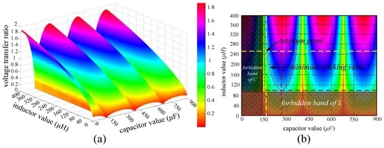
Figure 3.
Variation of Z-source elements (a) voltage transfer ratio via C and L; (b) minimum tracking value of L and C.

Table 1.
The parameters of the tested induction motor.
According to [24,25], satisfying the inequality of Equation (9) is the necessary condition for choosing the value of L and C which introduces boundaries for the L and C values as depicted in Figure 3b.
where, D0 is the shoot-through duty cycle and has been defined by T0/T, fs is the switching frequency. The ripple of capacitor voltage is shown as R1(dUc/Uc) and inductive current as R2(dIL/IL) in percentage.
It can be observed that the optimum value of capacitor and inductor is around 270 μF and 100 μH respectively. Since these values are not plausible, a feasible point should be determined from the tracking curve. As a result, the nearest feasible point of L and C to the optimum point can be achieved under the load condition as 250 μH and 170 μF, respectively. The values are obtained tentatively, with a feasible approximation, in order to reach maximized performance, reliability and cost-effectiveness, while minimizing the weight and volume of the overall Z-source topology. If the value of L < C then at least a pole of the transfer function of the whole system (by considering the equivalent impedance of IM) will be placed on the right side of the jὠ axis in the root-locus analysis. Therefore, according to Figure 3b, the minimum values for keeping the stability of the system are 250 μH and 170 μF. These values are empirically obtained by trying and error the possible values of tracking value diagram. It is worth mentioning that the values are selected based on the experimental model.
3. The Current Control of Voltage Source Inverter (VSI)
The relation between Ui and the rms value of the fundamental output line-to-line voltage is as follows:
Due to the DC property of Udc, its vector does not have an angle character and this introduces the magnitude of Udc. Moreover, the property of and is calculated in Equation (4). Therefore, by referring its ratio to the relation of and , then, the proportion of and can be extracted as follows:
As the first assumption of steady-state and rated conditions of the motor, can be considered as for the equivalent circuit of IM. The Udc on the same momentum needs to expand to where is the consequent vector from three abnormal input voltages and their substitution into Equation (11) gives the proportion shown below:
the output voltage and current, can deliver a constant range of power, which is enormously dependent on Udc and IL. If Va,refmax is assumed to be the reference vector with maximum amplitude then it matches the radius of the biggest circle that can encompass the hexagon by producing the abc unit as a reference. This can be seen in Figure 4.
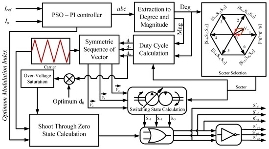
Figure 4.
Proposed Voltage Source inverter (VSI) control diagram.
The reference signal has been determined as the output phase current in the VSI control unit, which should be broken into , and elements and applied to the optimum PI controller by deducting the reference current value. Despite the fact that does not need to be modified in any special operation, the reference current value can be set based on the controlled d and q parameters and optimized PI controller output. With the inversion of and in the previous operation and the same as the previous stage, the value of the modulation index can be calculated by multiplying the coefficient by the modulation index, which comes from the PSO result.
4. The Optimum Control
The optimization problem that we consider here is motivated by the need to minimize the THD in the output current to a certain level. To achieve this, PSO is applied to the PI controllers to adjust the values. PSO is a meta-heuristic method in artificial intelligence that can be used to find approximate solutions to extremely difficult or impossible problems. PSO performance is comparable to that of genetic algorithms or the ant colony algorithm but it is faster and less complicated. It has been proven to be both very fast and effective when applied to a wide variety of optimization problems. In PSO, the potential solutions are called particles, and, in terms of their exploration and exploitation, the particles of the swarm fly through hyperspace and have two essential reasoning capabilities:
- Their memory of their own best position or local best (lb), which allows it to remember the best position in the feasible search space that has been visited, and
- Knowledge of the global or their neighborhood’s best or global best (gb), which is the best value obtained so far by any particle in the neighborhood of the particle.
The position of each particle in the swarm is updated using the following equation:
where x is the particle position and v is the particle velocity in the iteration k. The velocity is calculated as follows:
where, is the best individual particle position and is the best global position, c1 and c2 are the cognitive and social parameters, respectively; r1 and r2 are random numbers between 0 and 1. c1 and c2 are usually close to 2 and affect the size of the particle’s step towards the individual best and global best, respectively. In this study, both values are assumed to be 2 in order to attract the particle towards the best points equally.
, is called the cognitive component; the cognitive component acts as the particle’s memory, causing it to tend to return to the regions of the search space in which it has experienced high individual fitness.
, is called the social component, which causes the particle to tend to return to the best region the swarm has found so far and to follow the best neighbor’s direction. If c1 >> c2 then each particle is more attracted to the individual best position, conversely, if c2 >> c1, then the particles are more attracted to the global best position.
, called inertia, makes the particle move in the same direction and with the same velocity. In this work, inertia weight (w) starts with the maximum amount and decrease linearly during evolution, which provides a balance between global and local explorations, thus, requiring less iteration on average to find a sufficiently optimal solution. The maximum inertia weight is set to 0.9 and the minimum is 0.4 which linearly decreases during a run and it is calculated according to the following equation:
where w is inertia weight and k is the current number of iterations. The flow diagram in Figure 5 illustrates the general model for PSO that is applied in this study.
Figure 5.
The proposed Particle Swarm Optimization (PSO) algorithm.
The problem described here has seven variables, which are the PI parameters for the closed-loop current control and coefficients for modulation index, reference current, and load current. In PSO, these variables are easily coded—that is, each particle has a dimension space of seven. Figure 6 illustrates the closed-loop controlling system and the parameters which are optimized by PSO in a d-q system.
Figure 6.
Particle Swarm Optimization-PI (PSO-PI) controller.
The variables to be controlled are the parameters of PI and controlling coefficients. The control objectives are the following: (1) decrease the THD level in output current; and (2) to control the output current to constantly follow the reference current.
The goal is to decrease the undesirable harmonics in output currents by optimizing the PI parameters and other controlling parameters. In addition, the difference between the peaks in the sinusoidal waveform of phases is also added to the fitness function in order to make the output current closer to normal three phase sinusoidal while the output is limited to the reference current. The fitness function computes as:
where k represents the a-b-c phase sequence of a three-phase ac power source, in is the rms current of nth harmonic and i1 is the fundamental frequency component of output current.
The purpose of using PSO in this paper is to find the optimum value of Kpd, Kpq, Kid Kiq, Gref, Gload, and Gmi as the output vector, by evaluating the cost function which is THD of output current in Equation (16). The Matlab® simulator software is used to apply and evaluate the performance of the proposed PSO-PI controller. To find the accurate value of the output vector, the boundary for the elements of this vector is initially set to [0,107]. The first run of the algorithm is executed with the initial boundary. The results indicated that the boundary should be reduced to [0,300]. Therefore, PSO explores within smaller search space for the next runs. As a result, the more precise output vector is achievable. The PSO results are depicted in detail in Figure 7. The maximum function evaluation is set to 6000. For better illustration of the result, the first twenty iterations are neglected and fifty critical points are selected from the total iterations.
Figure 7.
The results of optimizing (a) Kp–d–Ki–d; (b) Kp–q–Ki–q; (c) ; (d) ; and (e) .
The PSO method is applied in order to obtain the best output of the system by adjusting the PI parameters. The optimum values for the proportional and the integral parameters selected to control d are 16.5444 and 4.0826; and for parameter q, they are 7.4637 and 5, respectively. The modulation index in the proposed method is controlled in real-time with a coefficient of reference current, 0.025, and load current of 0.026.The modulation index confident is 0.01962.
Although the voltage transfer ratio can be increased by reducing the modulation index, the stability of the system would be diminished owing to the approximate equivalency of D0 and D1 as depicted in Figure 8a. Hence, the modulation index cannot be stepped down less than 50%, but it is an essential property for driving an IM that being able to reach 0–1 interval of modulation index. Therefore, the value of modulation index is modified, which can be determined by the demand value at the reference point of current as follows:
Figure 8.
The voltage transfer ratio to the variation of (a) the modulation index; (b) the reference current and modulation index.
Figure 8b shows the possible value of modified modulation index based on the maximum and minimum value of current reference. The boundary of the maximum current is set to starting current of tested IM (7.8A), which results the modulation index equal to 0.842 and voltage transfer ratio 0.19 more than unity.
5. Simulation Results
The optimized current controlled Ultra Sparse Z-source Matrix Converter (USZSMC) is simulated at various operating conditions using the Matlab/Simulink® software. In this investigation, the switching frequency is fixed at 10 kHz for all benchmarks of the system. By applying any changes in current or frequency, the modulation index can be automatically adjusted and respond to changes without additional optimization or changing the PI parameters in the system. The optimization process is off-line which doesn’t require heavy online computation for modifying PI parameters.
5.1. Steady-State Response
In Figure 9a the abnormal grid voltage, phases a, b, and c are depicted besides the corresponding 3-phase input current. The equations of phase a, b, and c are considered as 380sin(ωt − 20°), 228sin(ωt − 110°), and 304sin(ωt + 139°) respectively. The virtual DC-link voltage which is the current source rectifier (CSR) output (Udc) and applied voltage as the DC output voltage of the Z-source network (Ui) are also shown in Figure 9b. It points out the boost-up level of the DC-link from the average 304 to 380 V. The unity voltage transfer ratio is determined with respect to the minimum compensation of Z-source. Therefore, the reference point seeks the hypothesis for the normal input voltage with 380 V.
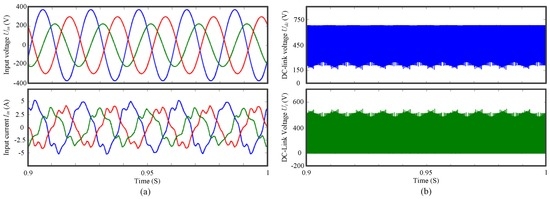
Figure 9.
Input (a) abnormal-grid voltage and current; (b) abnormal supplied for DC-link voltage after and before Z-source.
In abnormal conditions, the proposed system has been compared with the conventional Z-source matrix converter including PI controller in which PI controller parameters are tuned with the ZN method. These two systems have been tested with an identical input voltage as shown in Figure 9a. The input current is relatively distorted, which is not an issue, especially when the main application of this system has been assumed to be aerospace. A comparison between the response of the conventional and proposed models is depicted in Figure 10a,b. The achieved THD of the conventional model is 5.43% which is more than 3-fold the proposed method value (1.66%). Comparison of the disturbance accumulation can show each harmonic. The output voltage quality of both methods are shown in Figure 10c,d. In the proposed model, the maximum range of the voltage does not go beyond 600 V without any continual surge, while it even reaches 1 KV in the ordinary prototype.
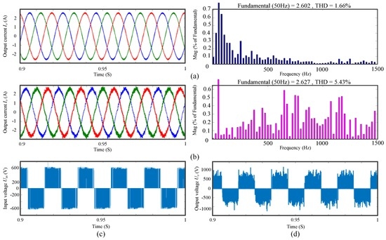
Figure 10.
Output current and voltage with abnormal supply under rated condition (a) output current and its total harmonic distortion (THD) with proposed method; (b) output current and its THD with conventional method; (c) output voltage with proposed method; (d) output voltage with conventional method.
The functionality of the system has been tested under distorted input voltage. Beside corresponding input current, the distorted input voltage that includes 15% of 3rd and 10% of 5th harmonics is illustrated in Figure 11a. Figure 11b depicts the Udc and Ui as the DC-link voltage before and after the Z-source, respectively.
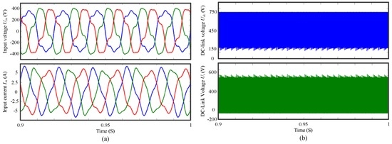
Figure 11.
Input (a) distorted-grid voltage and current; (b) distorted supplied for DC-link voltage after and before Z-source.
Obviously, the quality of output current is as suitable as an abnormal test done. It can be applied for driving the mentioned IM as can be seen in Figure 12a. Although, the quality of output voltage in abnormal conditions is relatively preferable than this test, the output voltage condition of this test is fairly better than in the conventional model, as can be seen in Figure 12b.
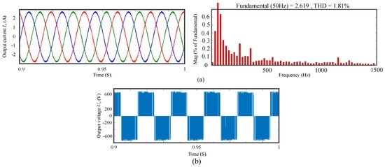
Figure 12.
Output current and voltage with distorted supply under rated condition (a) output current and its THD; (b) output voltage.
5.2. Dynamic Response
Dynamic analysis has been simulated after 0.75 s in order to allow IM be stabilized under the rated conditions. The transient duration has been illustrated in Figure 13. In this section, the magnitude and frequency reference values of output current vary during 300 ms to demonstrate the system dynamic response (Figure 14a,b). After reaching the rated speed at 0.75 s, the system remained operating with full load current until one second. For the magnitude responses, the reference value decreases to 50% and increases to 80% of full load current followed by a 60% fall to express the reliability of the control system toward load fluctuations. By applying the same conditions, the reference value remains at nominal frequency (50 Hz) between 0.75 s and 1 s. Afterwards, the frequency fluctuates among 30 Hz, 65 Hz and 40 Hz with 0.3 s time interval, respectively.
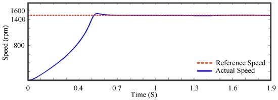
Figure 13.
The speed curve of induction motor (IM).
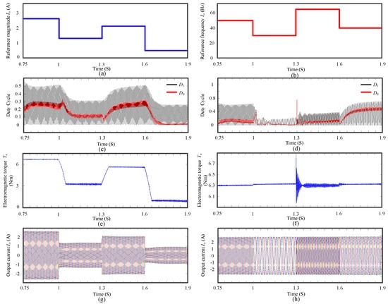
Figure 14.
Dynamic response to changing magnitude and frequency in the output current (a) The reference point of output current for magnitude; (b) The reference point of output current for frequency; (c) D0 and D1 variation in magnitude changes; (d) D0 and D1 variation in frequency changes; (e) electromagnetic torque variation in magnitude changes; (f) electromagnetic torque variation in frequency changes; (g) 3-phase stator current in magnitude changes; and (h) 3-phase stator current in frequency changes.
The variation of D0 and D1 for the duty cycle of shoot-through and non-shoot-through states are shown for the magnitude and frequency response in Figure 14c,d respectively. It shows the functionality of the timing optimization algorithm. As can be seen in Figure 14e,f, the IM electromagnetic torque varies simultaneously with the reference value in magnitude while it is constant for changing the frequency. The actual output current follows the alteration in the magnitude and frequency of reference current which are depicted in Figure 14g,h.
Figure 15 depicts the THD analysis of actual output current for both magnitude and frequency responses for each time interval separately. For the 50%, 80% and 20% of full load current; the achieved THDs are 2.41%, 1.86% and 2.39%, respectively. The variation outcomes in the load suggest that the proposed system compensates the degree of THD increase with respect to the load fluctuations. At the fundamental frequencies of 30, 65 and 40 Hz, the THD levels are 1.28, 2.46 and 1.31 percent, respectively.
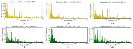
Figure 15.
THD analysis of output current with (a) 50%; (b) 80% ;(c) 20% of full-load current; (d) 30 Hz; (e) 65 Hz; and (f) 40 Hz.
6. Experimental Results
To verify the feasibility and effectiveness of the proposed scheme, an USZSMC was implemented with its current control strategy connected to an abnormal 3-phase network through a variable abnormal AC power supply to feed a 1 kW 3-phase IM. The proposed topology and control method were experimentally tested using the experimental prototype shown in Figure 16 with the same motor parameters as those for the simulation listed in Table 1. The component values chosen for the simulation were similar to those assembled for the hardware setup.
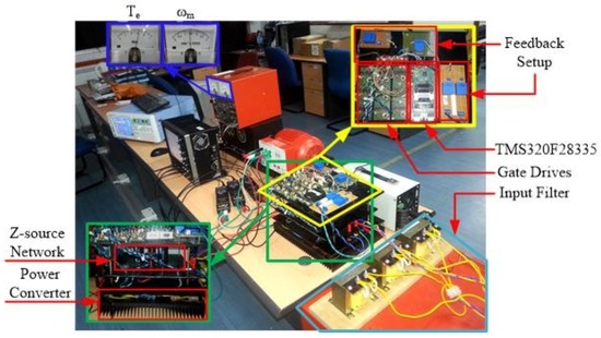
Figure 16.
Photograph of the experimental setup.
In order to diminish the harmonics of switching, an input filter was designed based on the values as performed in simulation (Lf = 1 mH and Cf = 10 μF).The USZSMC switching was configured using IKW40N120H3 (Infineon, Munich, Germany) and IGW30N60T IGBTs (Infineon, Munich, Germany) and an IDP30E120 diode (Infineon, Munich, Germany), as shown in Figure 16. The bottom level of the framework includes the ultra-sparse rectifier and two-stage inverter; the mid-level consists of the Z-source network elements with no sensor for detecting the voltage of capacitor or current of the inductor; and the overhead level comprises gate drives, controlling unit process, and feedback setup. The closed-loop control was carried out using a TMS320F28335 (Texas Instruments, Dallas, TX, USA) digital signal processor (DSP). The flowchart for programming the DSP is depicted in Figure 17.
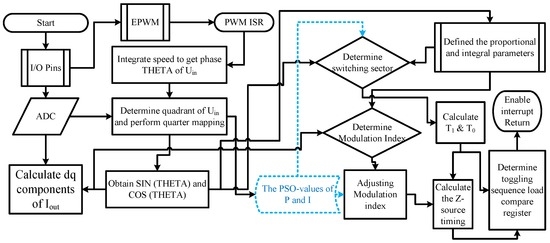
Figure 17.
The flowchart to program digital signal processor (DSP).
6.1. Steady-State Response
Steady-state performance has been tested under the condition which the abnormal voltage is supplied as illustrated in Figure 18a. The abnormal condition is defined: Ua = 380 V and |Δ∅Ua|=20°, Ub = 228 V and |Δ∅Ub| = 10°, Uc = 304 V and |Δ∅Uc| = 19°. As it can be calculated based on Enjeti’s method [26], Ub and Uc can be considered with a 40% and 20% abnormality rate from Ua, respectively. Figure 18b illustrates the input voltage (Uia) and input currents (Isa) after and before filter for phase a, which proves the unity of input power (cosφ). Figure 18c also depicts the virtual DC-links voltage for after (Ui) and before (Udc) Z-source network at the steady state and rated condition of IM by applying the shoot-through duty cycle. Figure 19a,b show the output voltage and current waveforms.
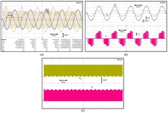
Figure 18.
Steady-state performance (a) three phase abnormal input voltage; (b) input current after and before filter; and (c) voltage of Udc (after Z-source) and Ui (before Z-source) at DC-link.
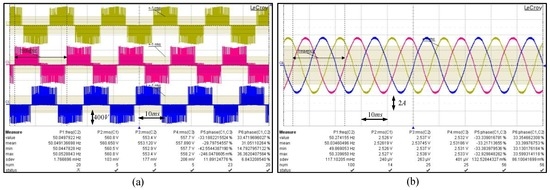
Figure 19.
Steady-state performance (a) output three phase voltage; (b) stator current.
Figure 20 shows the experimental Fast Fourier transform (FFT) analysis, which verifies the simulated THD results. In Figure 20a, the harmonics spectrum is depicted for the range of frequency between 5 Hz and 250 Hz for unfiltered input current at the converter side of the filter. The harmonics spectrum for the input current on the grid side of filter is also shown in Figure 20b. The FFT analysis of the output current and voltage are presented in Figure 20c,d respectively.
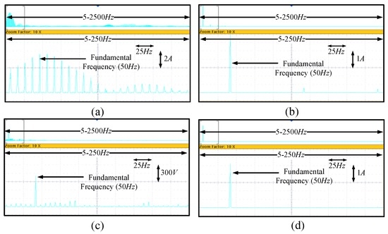
Figure 20.
Fast Fourier transform (FFT) Analysis around fundamental frequency (a) input current on converter side of filter; (b) input current on grid side of filter; (c) output voltage; and (d) output current.
6.2. Dynamic Response
In Figure 21, the magnitude of current, torque and speed are non-dimensionlised by the empirical formula as follows:
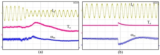
Figure 21.
Dynamic response of electromagnetic torque and rotor speed for variable of (a) magnitude; (b) frequency.
Non-dimensionalisation allows comparing cases of different scale directly because the results are proportional to the non-dimensionalising parameter. Therefore, the ripple of rotor speed and electromagnetic torque is not on the same scale as their waveforms. Figure 21a shows the waveforms for the stator current of the IM driven by the proposed method with the current reference value stepping down from 2.6 A (rated condition) to 50% of the full load, whereas the frequency is constant at 50 Hz. It is concluded that the proposed method has the advantage of a fast dynamic response with acceptable THD in terms of changing the amplitude while the electromagnetic torque is diminished to half of rated Te and the rotor speed is kept constant, except during the transient time. Figure 21b displays the waveforms balanced stator current of the IM driven by the proposed method with a frequency step up from 50 Hz to 60 Hz while the reference current is kept constant at the rated condition of 2.6 A. The experimental results show that with an abrupt change in frequency, the magnitude does not change.
7. Discussion
In the proposed method, the THD percentage of output current shows a minor increase but does not exceed 2.64% in the recommended testing margin while the rate of load current is reduced. Furthermore, in the conventional method, a relatively close to linear relation with a sharper slope between the load reduction and the increase in the output current THD exists. Regardless of the 1.08% lapse in the steady state for the output current and 0.82% for the output voltage, the proposed method achieves the exact target.
Referring to the transfer function of system as shown in Equation (8), at least two sensors, one current sensor for monitoring the current of L and a voltage sensor to detect the Udc or Ui, are eliminated from the Z-source for determining the boost factor. Table 2 shows a comparison between the results of this work and the other Z-source matrix converters in different reports in terms of quantity of elements in topology, maximum voltage transfer ratio, the quantity and values of Z-source elements, switching frequency, output current THD and maximum tolerated abnormality of input voltage. The proposed strategy drives an IM under 40% abnormal input voltage, while [27,28,29,30] have launched the static RL load. In the recommended topology, the overall volume and weight of the system is 2.3 L which is considerably lower than the conventional back-to-back converter with a volume of 4.6 L for the same power rating and thermal limitation of the USMC described in [31,32]. Moreover, the response of the proposed driving method is fast and accurate enough to be applied in the sensitive applications such as the aerospace industry.
Table 2.
Comparison of the performance of Z-source Matrix Converter with other findings.
8. Conclusions
This paper presents a d-q current control for driving an IM fed by USZSMC. USMC topology is employed based on it being one of the lightest forms of the IMC. To minimize the total size of the system, Z-source parameters are determined using both the timing and circuit approaches. The obtained results can be used in a practical model by a feasible approximation. The meta-heuristic algorithm of the PSO-PI controller is integrated with a rotational d-q current control method in order to determine the optimum coefficient values in a single multimodal problem. This control scheme can consider the inter-correlations of the other elements and the PI parameters together. The system has been tested for the unbalanced (40%), phase shifted (32°), and distorted (15%) input voltage. By applying this compensation method, the control algorithm could properly reduce the THD of the output current to 1.66%. The simulation and experimental results demonstrate that the proposed system produces sinusoidal currents of high quality at the output and acceptable ones at the input.
Acknowledgments
This work was supported by the High Impact Research of the University of Malaya—Ministry of Higher Education of Malaysia under Project UM.C/HIR/MOHE/ENG/24 and PPP grant PG179-2015.
Author Contributions
Seyed Sina Sebtahmadi has contributed to the theoretical approaches (power transmission, motor drive, and optimization), simulation, experimental tests, and preparing the article; Hanieh Borhan Azad has contributed to the theoretical approaches (optimization), simulations, experimental tests, and preparing the article; Didarul Islam has contributed to the theoretical approaches (power transmission, motor drive), simulation, experimental tests, and preparing the article; Mehdi Seyedmahmoudian has contributed to the theoretical approaches (optimization), simulations, experimental tests, and preparing the article; Ben Horan has contributed to the theoretical approaches (optimization), simulations, experimental tests, and preparing the article; Saad Mekhilef has contributed to the theoretical approaches (power transmission, motor drive, and optimization), simulation, experimental tests, and preparing the article. Moreover, he has supervised this research.
Conflicts of Interest
The authors declare no conflict of interest.
References
- Brunson, C.; Empringham, L.; de Lillo, L.; Wheeler, P.; Clare, J. Open-Circuit Fault Detection and Diagnosis in Matrix Converters. IEEE Trans. Power Electron. 2015, 30, 2840–2847. [Google Scholar] [CrossRef]
- Sun, Y.; Li, X.; Su, M.; Wang, H.; Dan, H.; Xiong, W. Indirect Matrix Converter-Based Topology and Modulation Schemes for Enhancing Input Reactive Power Capability. IEEE Trans. Power Electron. 2015, 30, 4669–4681. [Google Scholar] [CrossRef]
- Liu, X.; Wang, P.; Loh, P.C.; Blaabjerg, F. A three-phase dual-input matrix converter for grid integration of two AC type energy resources. IEEE Trans. Ind. Electron. 2013, 60, 20–30. [Google Scholar] [CrossRef]
- Andreu, J.; Kortabarria, I.; Ormaetxea, E.; Ibarra, E.; Martin, J.L.; Apiñaniz, S. A step forward towards the development of reliable matrix converters. IEEE Trans. Ind. Electron. 2012, 59, 167–183. [Google Scholar] [CrossRef]
- Sebtahmadi, S.; Pirasteh, H.; Kaboli, S.; Radan, A.; Mekhilef, S. A 12-Sector Space Vector Switching Scheme for Performance Improvement of Matrix-Converter-Based DTC of IM Drive. IEEE Trans. Power Electron. 2015, 30, 3804–3817. [Google Scholar] [CrossRef]
- Song, W.; Zhong, Y.; Zhang, H.; Sun, X.; Zhang, Q.; Wang, W. A study of Z-source dual-bridge matrix converter immune to abnormal input voltage disturbance and with high voltage transfer ratio. IEEE Trans. Ind. Inform. 2013, 9, 828–838. [Google Scholar] [CrossRef]
- Karaman, E.; Farasat, M.; Trzynadlowski, A.M. A comparative study of series and cascaded Z-source matrix converters. IEEE Trans. Ind. Electron. 2014, 61, 5164–5173. [Google Scholar] [CrossRef]
- Aten, M.; Towers, G.; Whitley, C.; Wheeler, P.; Clare, J.; Bradley, K. Reliability comparison of matrix and other converter topologies. IEEE Trans. Aerosp. Electron. Syst. 2006, 42, 867–875. [Google Scholar] [CrossRef]
- Li, X.; Su, M.; Sun, Y.; Dan, H.; Xiong, W. Modulation strategies based on mathematical construction method for matrix converter under unbalanced input voltages. IET Power Electron. 2013, 6, 434–445. [Google Scholar] [CrossRef]
- Yousefi-Talouki, A.; Pellegrino, G.; Mengoni, M.; Zarri, L. Self-commissioning algorithm for matrix converter, nonlinearity compensation. In Proceedings of the 2015 IEEE Energy Conversion Congress and Exposition (ECCE), Montreal, QC, Canada, 20–24 September 2015; pp. 4077–4083.
- Schönberger, J.; Friedli, T.; Round, S.; Kolar, J. An ultra sparse matrix converter with a novel active clamp circuit. In Proceedings of the Power Conversion Conference (PCC’07), Nagoya, Japan, 2–5 April 2007; pp. 784–791.
- Siwakoti, Y.P.; Peng, F.Z.; Blaabjerg, F.; Loh, P.C.; Town, G.E. Impedance-source networks for electric power conversion part I: A topological review. IEEE Trans. Power Electron. 2015, 30, 699–716. [Google Scholar] [CrossRef]
- Trentin, A.; Zanchetta, P.; Empringham, L.; de Lillo, L.; Wheeler, P.; Clare, J. Experimental comparison between direct matrix converter and indirect matrix converter based on efficiency. In Proceedings of the 2015 IEEE Energy Conversion Congress and Exposition (ECCE), Montreal, QC, Canada, 20–24 September 2015; pp. 2580–2587.
- Rohouma, W.; Zanchetta, P.; Wheeler, P.W.; Empringham, L. A Four-Leg Matrix Converter Ground Power Unit with Repetitive Voltage Control. IEEE Trans. Power Electron. 2015, 62, 2032–2040. [Google Scholar] [CrossRef]
- Corres, J.M.; Bravo, J.; Arregui, F.J.; Matias, I.R. Unbalance and harmonics detection in induction motors using an optical fiber sensor. IEEE Sens. J. 2006, 6, 605–612. [Google Scholar] [CrossRef]
- Al-Badri, M.; Pillay, P.; Angers, P. A Novel Full-Load Efficiency Estimation Technique for Induction Motors Operating with Unbalanced Voltages. IEEE Trans. Ind. Appl. 2016, 52, 2843–2855. [Google Scholar] [CrossRef]
- Kai, S.; Daning, Z.; Lipei, H.; Matsuse, K. Compensation control of matrix converter fed induction motor drive under abnormal input voltage conditions. In Proceedings of the 2004 IEEE 39th IAS Annual Meeting Industry Applications Conference, Seattle, WA, USA, 3–7 October 2004; pp. 1–630.
- Nielsen, P.; Blaabjerg, F.; Pedersen, J.K. Space vector modulated matrix converter with minimized number of switchings and a feedforward compensation of input voltage unbalance. In Proceedings of the 1996 International Conference on Power Electronics, Drives and Energy Systems for Industrial Growth, Delhi, India, 8–11 January 1996; Volume 2, pp. 833–839.
- Casadei, D.; Serra, G.; Tani, A. Reduction of the input current harmonic content in matrix converters under input/output unbalance. IEEE Trans. Ind. Electron. 1998, 45, 401–411. [Google Scholar] [CrossRef]
- Gozde, H. Comparative analysis of swarm optimization-based control method for direct matrix converter. Electr. Eng. 2015, 97, 1–13. [Google Scholar] [CrossRef]
- Ruiz-Cruz, R.; Sanchez, E.N.; Ornelas-Tellez, F.; Loukianov, A.G.; Harley, R.G. Particle swarm optimization for discrete-time inverse optimal control of a doubly fed induction generator. IEEE Trans. Cybern. 2013, 43, 1698–1709. [Google Scholar] [CrossRef] [PubMed]
- Siwakoti, Y.P.; Blaabjerg, F.; Loh, P.C.; Town, G.E. High-voltage boost quasi-Z-source isolated DC/DC converter. IET Power Electron. 2014, 7, 2387–2395. [Google Scholar] [CrossRef]
- Zheng, P.F. Z-source inverter. IEEE Trans. Ind. Appl. 2003, 39, 504–510. [Google Scholar] [CrossRef]
- Liu, S.; Ge, B.; Jiang, X.; Abu-Rub, H.; Peng, F.Z. Comparative Evaluation of Three Z-Source/Quasi-Z-Source Indirect Matrix Converters. IEEE Trans. Ind. Electron. 2015, 62, 692–701. [Google Scholar] [CrossRef]
- Shen, M.; Joseph, A.; Wang, J.; Peng, F.Z.; Adams, D.J. Comparison of traditional inverters and Z-source inverter for fuel cell vehicles. IEEE Trans. Power Electron. 2007, 22, 1453–1463. [Google Scholar] [CrossRef]
- Enjeti, P.N.; Choudhury, S.A. A new control strategy to improve the performance of a PWM AC to DC converter under unbalanced operating conditions. IEEE Trans. Power Electron. 1993, 8, 493–500. [Google Scholar] [CrossRef]
- Liu, X.; Loh, P.C.; Wang, P.; Han, X. Improved modulation schemes for indirect Z-source matrix converter with sinusoidal input and output waveforms. IEEE Trans. Power Electron. 2012, 27, 4039–4050. [Google Scholar] [CrossRef]
- Wijekoon, T.; Klumpner, C.; Zanchetta, P.; Wheeler, P.W. Implementation of a hybrid AC–AC direct power converter with unity voltage transfer. IEEE Trans. Power Electron. 2008, 23, 1918–1926. [Google Scholar] [CrossRef]
- Klumpner, C. A hybrid indirect matrix converter immune to unbalanced voltage supply, with reduced switching losses and improved voltage transfer ratio. In Proceedings of the 21st Annual IEEE Applied Power Electronics Conference and Exposition (APEC’06), Dallas, TX, USA, 19–23 March 2006; p. 7.
- Park, K.; Lee, K.-B.; Blaabjerg, F. Improving output performance of a Z-source sparse matrix converter under unbalanced input-voltage conditions. IEEE Trans. Power Electron. 2012, 27, 2043–2054. [Google Scholar] [CrossRef]
- Kolar, J.W.; Schafmeister, F.; Round, S.D.; Ertl, H. Novel three-phase AC–AC sparse matrix converters. IEEE Trans. Power Electron. 2007, 22, 1649–1661. [Google Scholar] [CrossRef]
- Round, S.; Schafmeister, F.; Heldwein, M.; Pereira, E.; Serpa, L.; Kolar, J. Comparison of performance and realization effort of a very sparse matrix converter to a voltage DC link pwm inverter with active front end. Inst. Electr. Eng. J. (Ind. Appl. Mag.) 2006, 126, 578–588. [Google Scholar] [CrossRef]
© 2016 by the authors; licensee MDPI, Basel, Switzerland. This article is an open access article distributed under the terms and conditions of the Creative Commons Attribution (CC-BY) license (http://creativecommons.org/licenses/by/4.0/).