1. Introduction
Many high-output-voltage applications, such as large-capacity photovoltaic power generation for DC transmission and offshore wind power delivery, require the conversion of low-voltage input to high-voltage output [
1,
2]. In these scenarios, the higher input current and output voltage exacerbate the current and voltage stress on devices [
3].
The input-parallel output-series (IPOS) LLC resonant converter with multiple modules is an effective solution to the aforementioned issues [
4,
5,
6,
7]. This topology not only significantly reduces the voltage and current stress on power devices but also enhances the system’s output voltage level and power capacity. However, in practical applications, the LLC converter based on the IPOS topology is prone to imbalances in output voltage and input current due to unavoidable manufacturing discrepancies in the resonant tank components of each module. These imbalances can adversely affect the device’s heat dissipation, shorten its lifespan, and, in severe cases, lead to module damage due to overvoltage and overcurrent stress, threatening the overall stability of the power conversion system [
8]. Consequently, the issue of output voltage equalization and input current sharing in IPOS-based LLC resonant converters has become a focal point of attention in both academia and industry.
A substantial amount of research has been conducted on the issue of voltage equalization and current sharing in IPOS-based LLC resonant converters. The core idea is to achieve impedance matching between phases. These research approaches can be broadly classified into two categories: active and passive methods [
9].
In active voltage equalization and current-sharing schemes, reference [
10] proposes a maximum voltage equalization method that adjusts the voltage of each module by regulating the maximum output voltage, but this requires additional signal cascading and isolation. Researchers [
11] employed droop control to ensure power balance, though the control is complex, and voltage fluctuations may occur in the event of a failure in the main module. Authors [
12] implemented dual-loop control to achieve output voltage equalization at the series output of the IPOS converter, but it increases the number of components and sampling circuits, thereby raising costs and complexity. Others [
13,
14] regulated voltage gain using methods such as phase-shift control by sampling current to achieve voltage equalization and current sharing.
In passive voltage equalization and current-sharing schemes, Reference [
15] proposes a coupled transformer scheme that reduces the magnetic core size and achieves output voltage balance through flux cancellation. However, the transformer design is complex, and it places high demands on core materials and flux control, which increase the system’s cost and design difficulty. Reference [
16] proposes paralleling two-phase resonant inductors to achieve automatic voltage equalization, but, under multi-resonant parameter mismatches, the effectiveness remains suboptimal.
To address the aforementioned issues, this paper proposes a shared inductance–capacitance LLC resonant IPOS converter. This method connects the resonant inductors and resonant capacitors of each phase of the LLC resonant converter in parallel through interconnection lines, achieving precise voltage equalization across all phases and input current sharing over the entire load range.
The sections of this paper are arranged as follows:
Section 2 reviews and analyzes the limitations of the traditional IPOS-type LLC resonant converter and the shared inductance structure.
Section 3 introduces in detail the voltage and current equalization principles and advantages of the proposed shared inductance–capacitance structure in the IPOS-type LLC converter and discusses the module expansion capabilities.
Section 4 analyzes the voltage and current equalization performance of the proposed method considering parasitic parameter mismatches.
Section 5 validates the effectiveness of the proposed method through simulations.
Section 6 develops a 1.25 kW two-phase experimental prototype and builds a testing platform, comparing it with traditional structures and the shared inductance structure to verify the effectiveness and superiority of the proposed topology.
Section 7 summarizes this research and describes future research directions.
2. Analysis of Traditional IPOS and Shared Inductance Issues
2.1. Analysis of Traditional IPOS Topology and Voltage–Current Equalization Performance
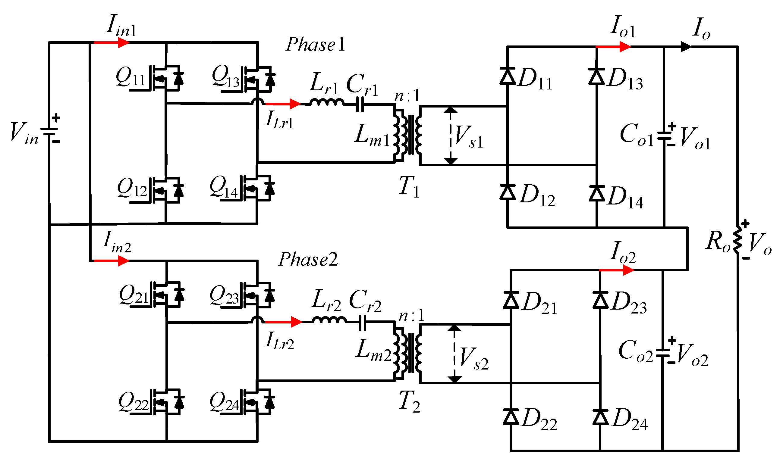
The IPOS LLC resonant converter topology is shown in
Figure 1. This topology employs an input-parallel, output-series configuration to achieve higher voltage gain. In the diagram,
Q11–
Q14 and
Q21–
Q24 are the primary-side switching devices of the two-phase LLC converter, while
Lr1,
Cr1, and
Lm1 are the resonant inductance, resonant capacitance, and magnetizing inductance of the first phase. Similarly,
Lr2,
Cr2, and
Lm2 are the resonant inductance, resonant capacitance, and magnetizing inductance of the second phase. In this topology, the two modules share the input current on the primary side and equally divide the output voltage on the secondary side, thereby achieving high power and high gain DC/DC conversion.
When there are deviations in the resonant tank parameters of the two modules, it causes a shift in the resonant frequency, leading to imbalances in the output voltage and input current. This results in excessive voltage and current stress on power devices, which affects the converter’s performance and reliability.
2.2. Analysis of Voltage and Current Equalization Performance in Interconnection-Line Shared Inductance Structure
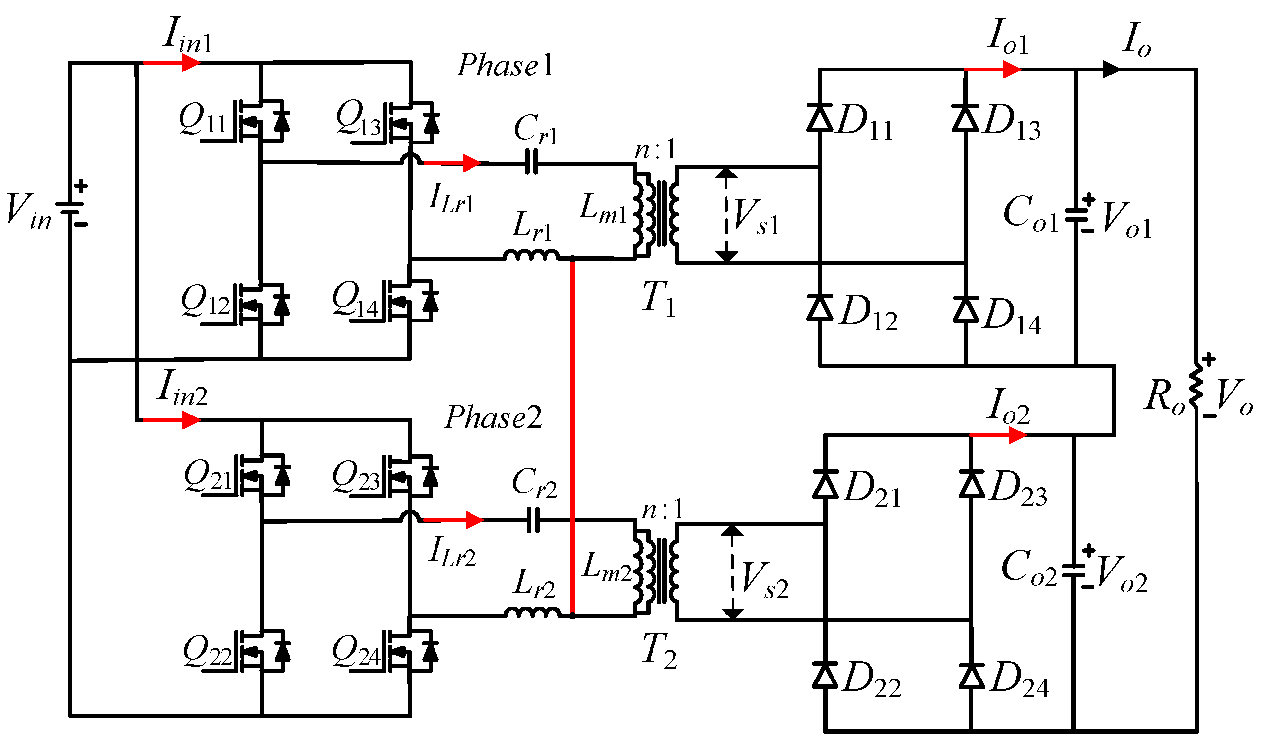
In reference [
16], a passive equalization scheme based on the interconnection-line shared inductance structure is proposed. This scheme achieves voltage and current equalization by paralleling resonant inductors between the two modules. The interconnection-line shared inductance topology is shown in
Figure 2.
To avoid lengthy derivations, this section briefly presents key equations for the shared inductance structure in reference [
16].
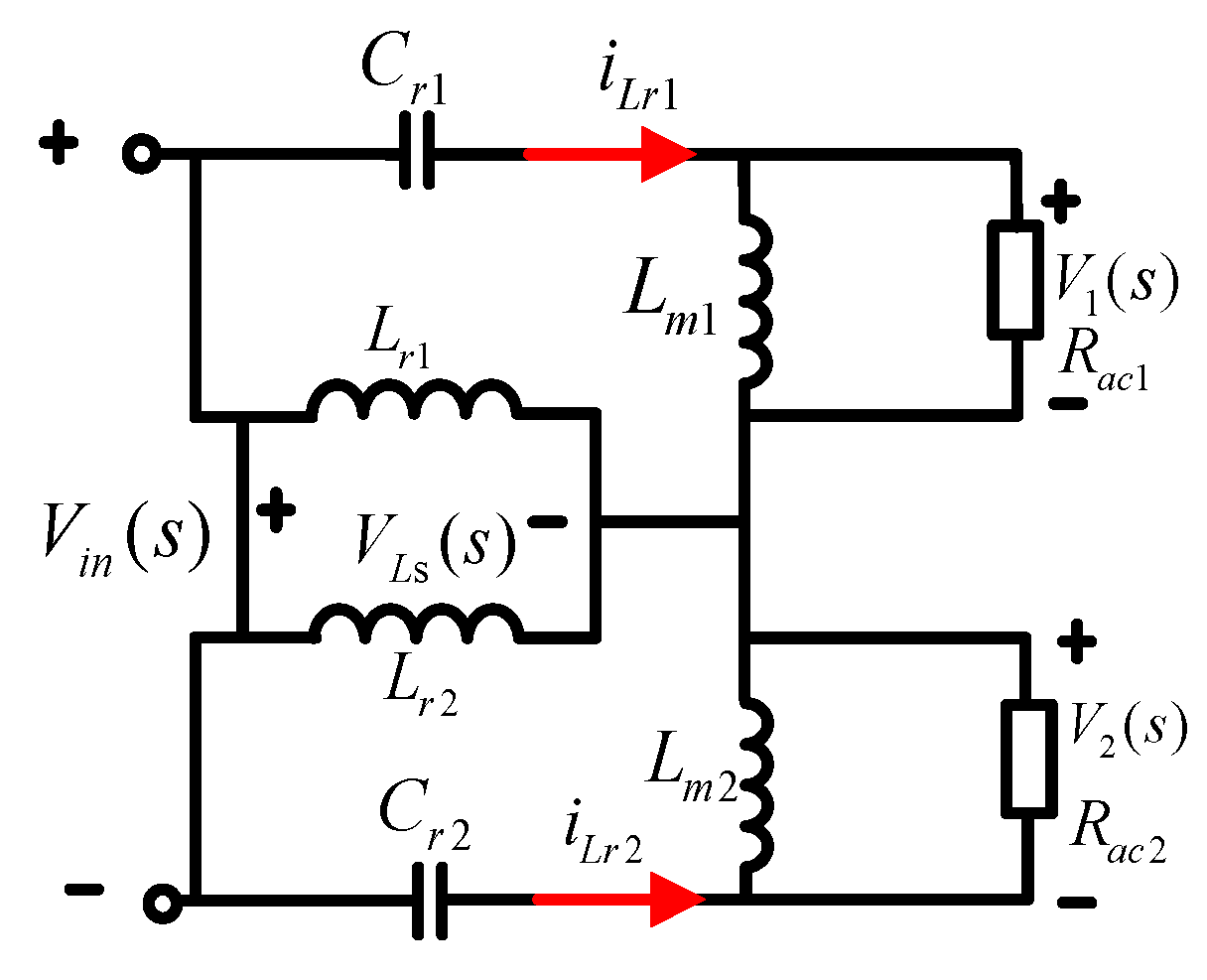
Figure 3 shows the equivalent circuit diagram of the interconnection-line shared inductance structure under the fundamental harmonic approximation. The coefficient
μ is defined as the voltage imbalance factor between the modules, and
Vin(s) and
VLs(s) represent the AC input voltage and inductor voltage in the fundamental harmonic equivalent circuit, respectively. The resonant currents for the two phases are denoted
iLr1 and
iLr2.
Rac1 and
Rac2 are the equivalent loads for the two phases, while
V1(
s) and
V2(
s) represent the equivalent fundamental wave voltages for the first and second phases, as expressed in Equation (1).
Based on the resonant tank voltage divider relationship,
V1(
s) and
V2(
s) can be expressed as:
By solving Equations (1) and (2) simultaneously, the voltage equalization error μ can be obtained.
Although the parallel inductors eliminate the imbalance in output voltage between the two phases caused by resonant inductance errors, the resonant capacitors and magnetizing inductance still affect the voltage equalization performance.
The relative relationship between the resonant currents of the two modules is:
According to Equation (3), when using the shared inductance structure, both phases share the same inductor. However, when there are still parameter differences in the resonant capacitors and magnetizing inductors of each module, the current-sharing characteristics of this scheme are limited. The currents are no longer independent, resulting in some degree of difference in the resonant currents between the modules, which affects the overall current-sharing performance.
Therefore, although the interconnection-line shared inductance structure can improve voltage and current equalization under certain conditions, the system’s balancing performance still has limitations when there are significant differences in the parameters of the resonant components, affecting the reliability and efficiency of the converter.
3. Proposed Shared Inductance–Capacitance Structure for Voltage and Current Equalization Characteristics
3.1. Proposed IPOS Shared Inductance–Capacitance Converter Topology
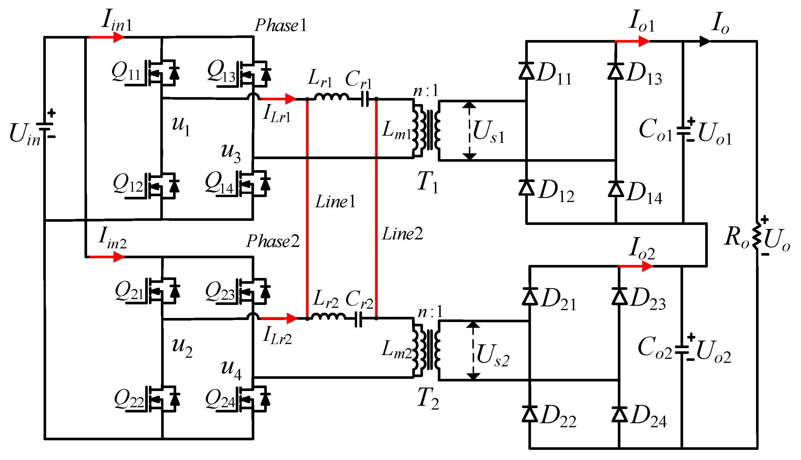
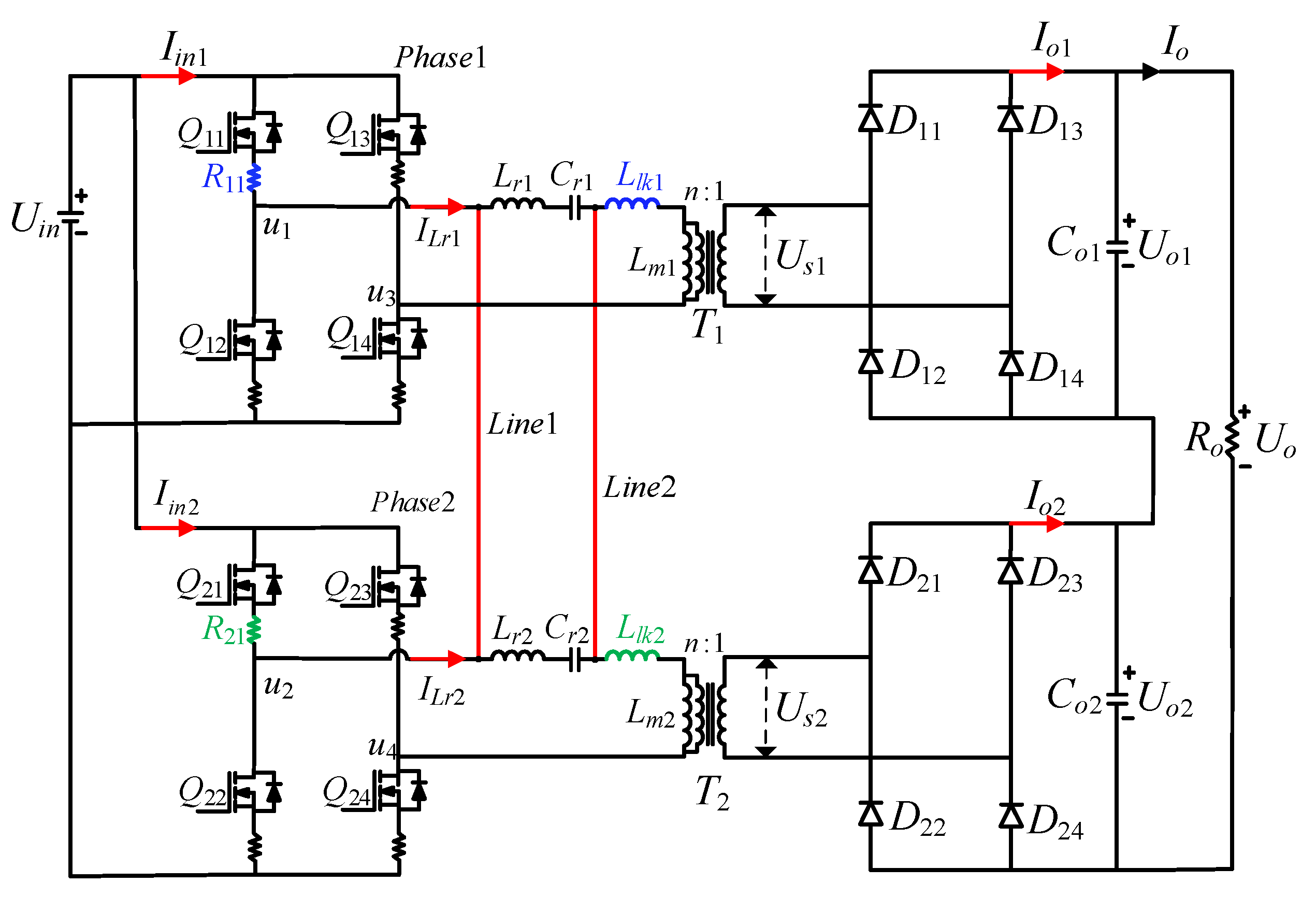
This section presents a topology for the interconnection-line shared inductance–capacitance self-balancing voltage and current equalization IPOS-type LLC resonant converter, shown in
Figure 4.
In
Figure 4, Line 1 and Line 2 represent the interconnection lines in the proposed topology. Line 1 and Line 2 connect the resonant inductors and resonant capacitors of Phase 1 and Phase 2 in parallel on the primary side, achieving mutual coupling between the two modules and forming a shared inductance–capacitance branch, thereby effectively balancing the input impedance between different modules.
During operation, the driving signals for the primary-side switches Q11, Q14, Q21, and Q24 are the same, while the driving signals for Q12, Q13, Q22, and Q23 are identical. Lr1, Cr1, and Lm1 represent the resonant inductance, resonant capacitance, and magnetizing inductance of phase 1, respectively. Lr2, Cr2, and Lm2 represent the resonant inductance, resonant capacitance, and magnetizing inductance of phase 2. Uo is the output voltage, and Uo1 and Uo2 are the output voltages of the two phases. u1 to u4 represent the bridge arm voltages of the two phases. n is the transformer turn ratio.
3.2. Fundamental Harmonic Approximation (FHA) Assumptions and Validity Limits
To analyze the voltage and current equalization system, this paper introduces the fundamental harmonic approximation (FHA). Before applying the FHA model, its assumptions, applicability, and limitations must be clarified.
- (a)
Basic Assumptions of FHA Model
FHA assumes the system’s voltage and current are dominated by the fundamental harmonic, ignoring higher-order harmonics. The voltage waveform is approximated as:
Here, V0 is the amplitude of the fundamental harmonic, ω is the resonance frequency, and ϕ is the phase. This assumption holds near the ideal resonance frequency, where it is assumed that the responses of the inductors and capacitors are linear, allowing the fundamental harmonic component to dominate.
While the FHA model is accurate under resonant conditions, it may fail under the following circumstances:
Non-resonant conditions: when deviating from resonance, higher-order harmonics significantly affect the balance, invalidating the model.
Partial load operation: nonlinearities and increased harmonics cause analysis deviations.
Significant harmonics: harmonics generated by operating condition fluctuations affect energy transfer and impedance matching, reducing model validity.
3.3. Voltage Equalization Analysis of the Proposed Structure
To quantitatively analyze the impact of parameter differences on the output voltage, the resonant tank parameter relationship is defined as shown in Equation (4). Using the parameters of the first phase of the resonant tank as the reference, error coefficients a, b, and c are introduced to represent the proportional relationships between the resonant inductance
Lr2, resonant capacitance
Cr2, and magnetizing inductance
Lm2 of the second phase and the corresponding parameters of the first phase of the resonant tank.
In the steady state, the total output voltage
Uo is composed of the output voltage of phase 1,
Uo1, and the output voltage of phase 2,
Uo2:
Since the output is a series configuration, it can be expressed as:
The equivalent load resistances for each phase,
Ro1 and
Ro2, as well as the total equivalent load
Ro, can be expressed as:
The coefficient
k is defined as the proportion of the total output voltage carried by the first phase’s output voltage. When
k = 0 or 1, it indicates that the voltage is handled by only one module, and when
k = 0.5, the voltage is evenly distributed between the two modules. Therefore, the output voltages
Uo1 and
Uo2 can be expressed as:
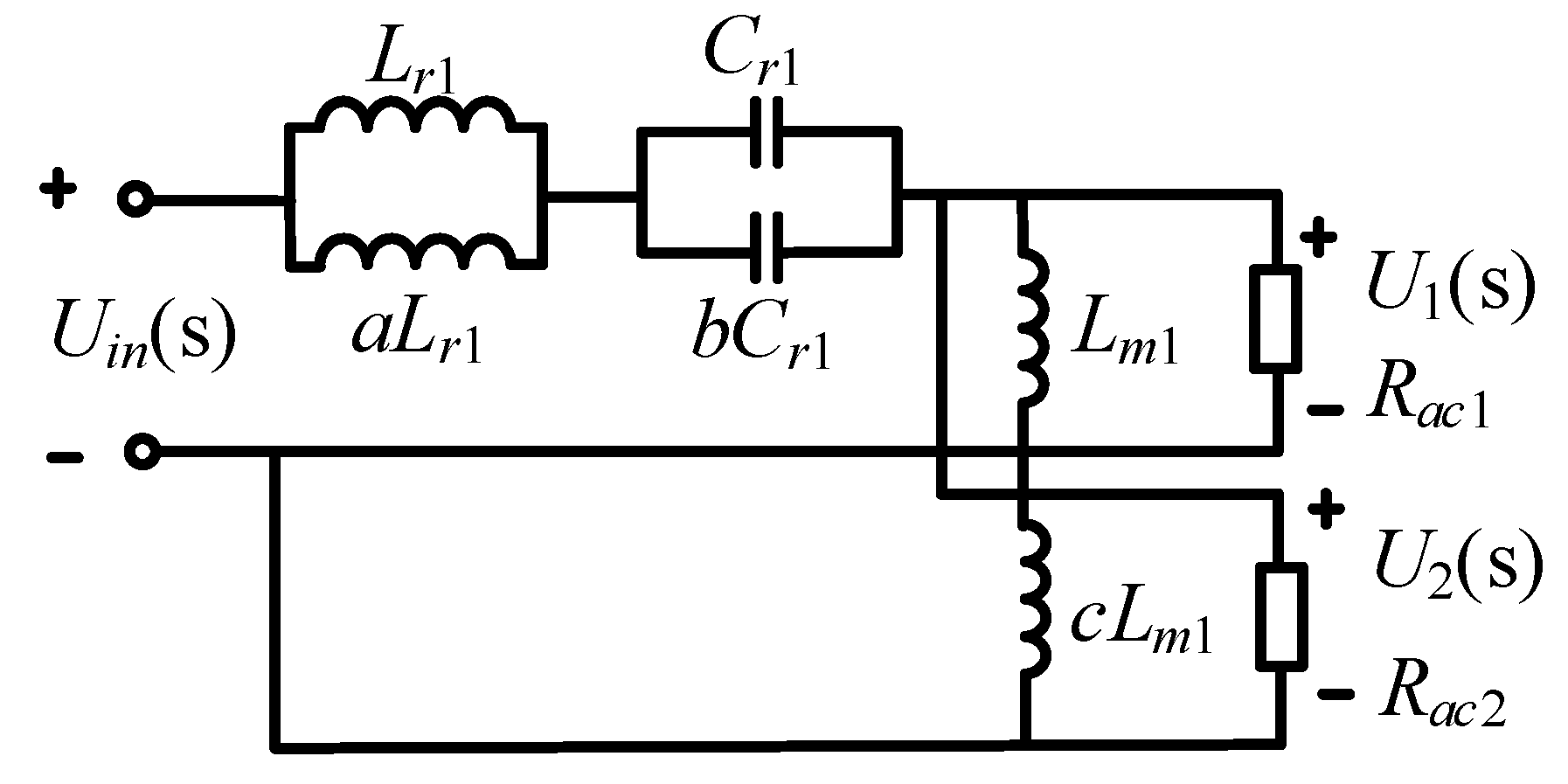
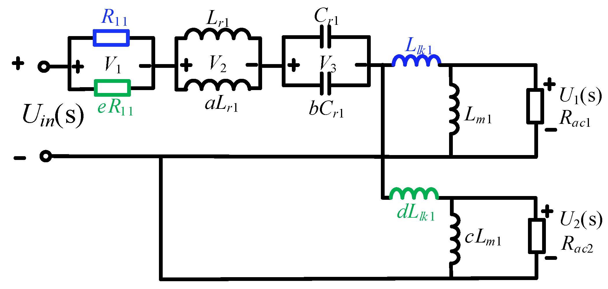
Figure 5 shows the equivalent circuit of the structure under the fundamental harmonic approximation.
Uin(
s) represents the AC input voltage in the fundamental harmonic equivalent circuit.
U1(
s) and
U2(
s) denote the equivalent fundamental wave voltages of the two phases, which can be expressed using coefficient
k.
Rac1 and
Rac2 are the equivalent loads for the two phases, and they are expressed in Equation (11).
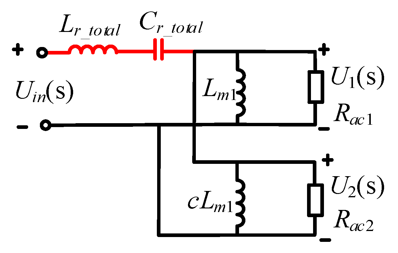
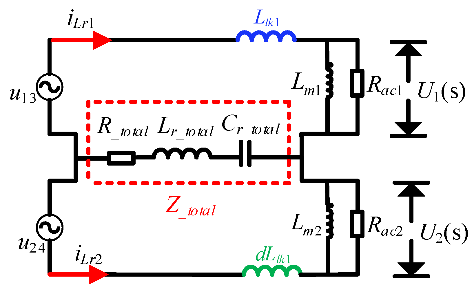
The simplified fundamental harmonic equivalent circuit of the shared inductance–capacitance structure is shown in
Figure 6. In this circuit,
Lr_total and
Cr_total represent the total resonant inductance and total resonant capacitance, respectively, and their expressions are given in Equation (12).
Unlike the shared inductance structure, in this case, the impedance divider relationship of
U1(
s) and
U2(
s) in the resonant tank changes. The expression for this relationship is given in Equation (13).
By solving Equations (10) and (13) simultaneously, the value of
k can be determined. Additionally, to evaluate the voltage equalization performance of the proposed structure, the load voltage equalization error
δv is defined, and its expression is:
According to Equation (13), when U1(s) equals U2(s), the voltage equalization error δv is 0, indicating that the output voltages of the two modules are equal.
3.4. Current-Sharing Analysis of the Proposed Structure
To simplify the analysis, it is assumed that the power devices of the two modules in
Figure 4 have the same driving signals and no delay:
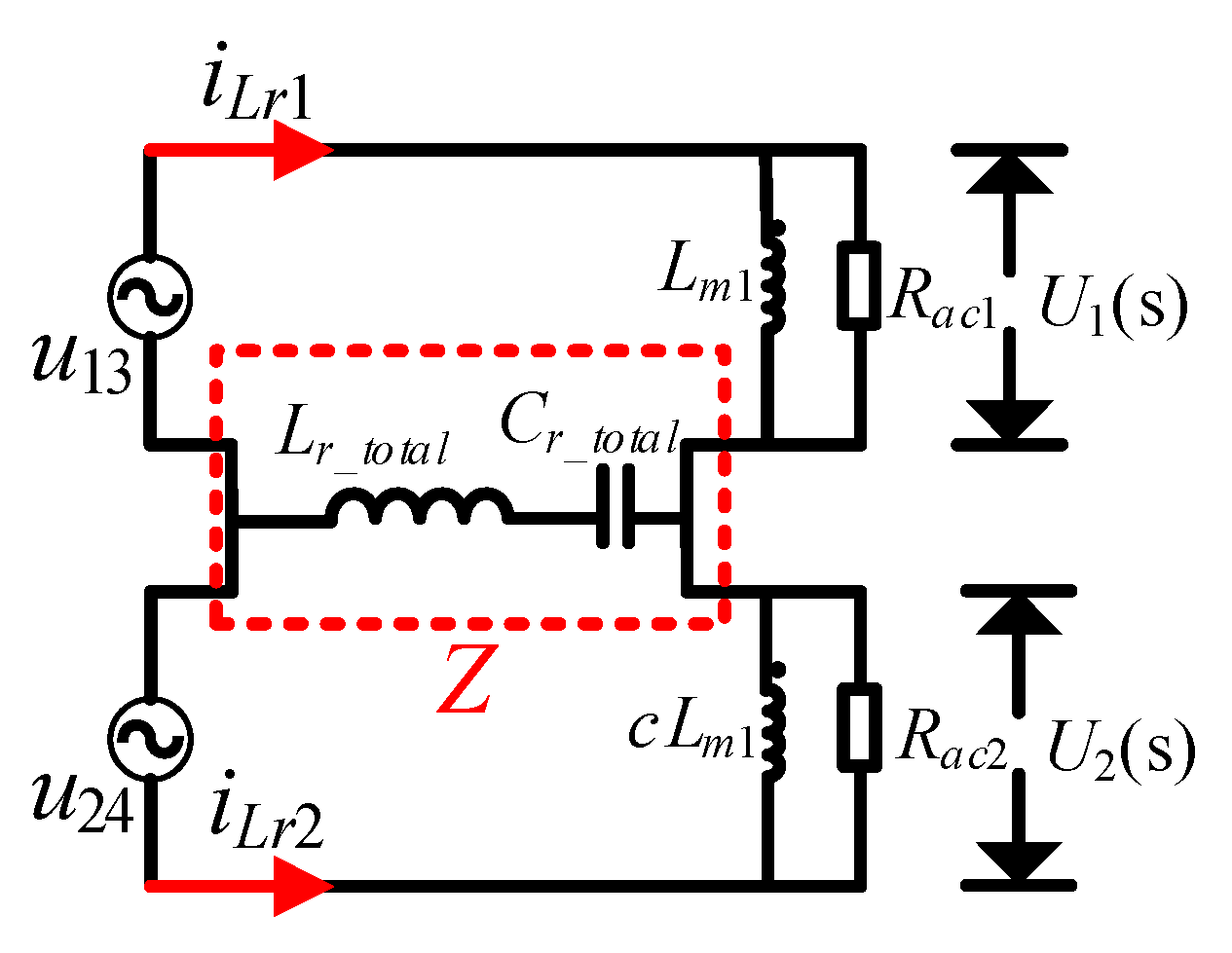
The equivalent circuit model of the shared inductance–capacitance structure is shown in
Figure 7.
The input voltage is given in Equation (16).
where
Due to the parallel output, u13 = u24. Combining Equations (16) and (17), it can be concluded that iLr1 and iLr2 are equal.
The current-sharing error
δi is defined as follows, where rms(
iLr1) and rms(
iLr2) represent the root mean square values of the resonant currents
iLr1 and
iLr2, respectively:
After the shared inductance–capacitance, the current-sharing error δi is 0, indicating that the input current is perfectly shared between the modules.
3.5. Comparison with Traditional Structure and Interconnection-Line Shared Inductance Structure
This section explores the quantitative sensitivity analysis of component tolerances for
Lr,
Cr, and
Lm. It investigates the impact of different combinations of error coefficients a, b, and c on the voltage equalization error
δv, considering the parameter variations in the actual manufacturing process. The resonant tank parameters are set with a ±10% tolerance, and thus the values of a, b and c range from {0.9, 1, 1.1}. Due to the symmetry of the different values, the combination (a = 0.9 b = 0.9 c = 0.9) has the same impact on the voltage equalization error
δv as the combination (a = 1.1 b = 1.1 c = 1.1). Therefore, there are 13 effective combinations covering all possible parameter variations within the ±10% tolerance range. The specific error combinations are shown in
Table 1, and the converter parameter indicators are shown in
Table 2.
The relationship between the output voltage equalization error
δv and switching frequencies for the traditional structure for all 13 error combinations in
Table 1 and the parameter indicators in
Table 2 are shown in
Figure 8.
As shown in
Figure 8, the output voltage error of the traditional structure significantly increases as the frequency decreases, with the maximum error occurring at 40 kHz. Its voltage equalization performance is sensitive to operating condition variations, exhibiting poor robustness.
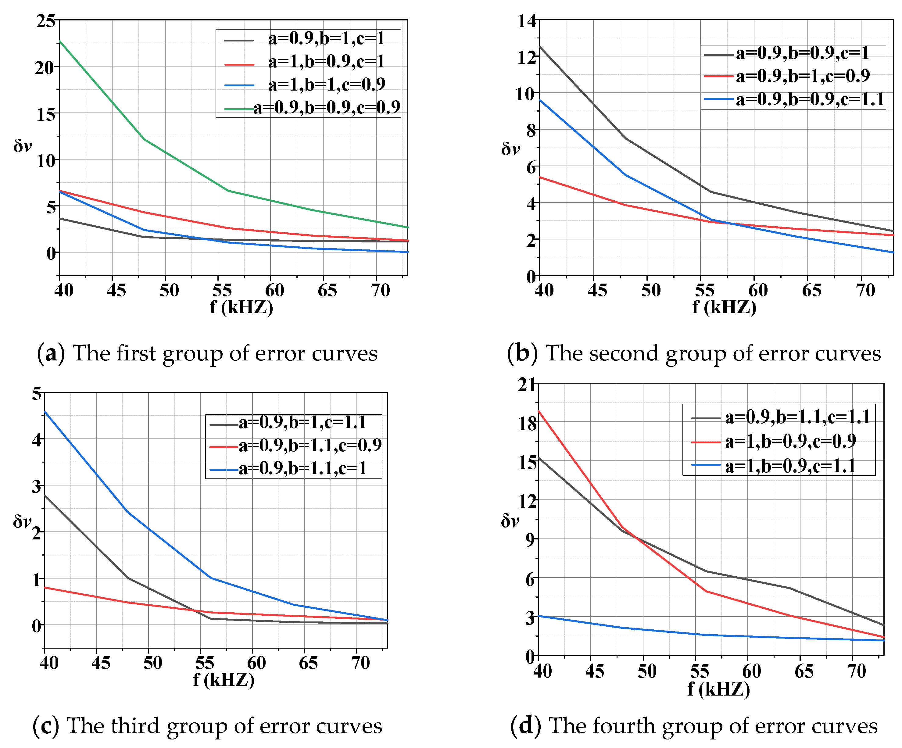
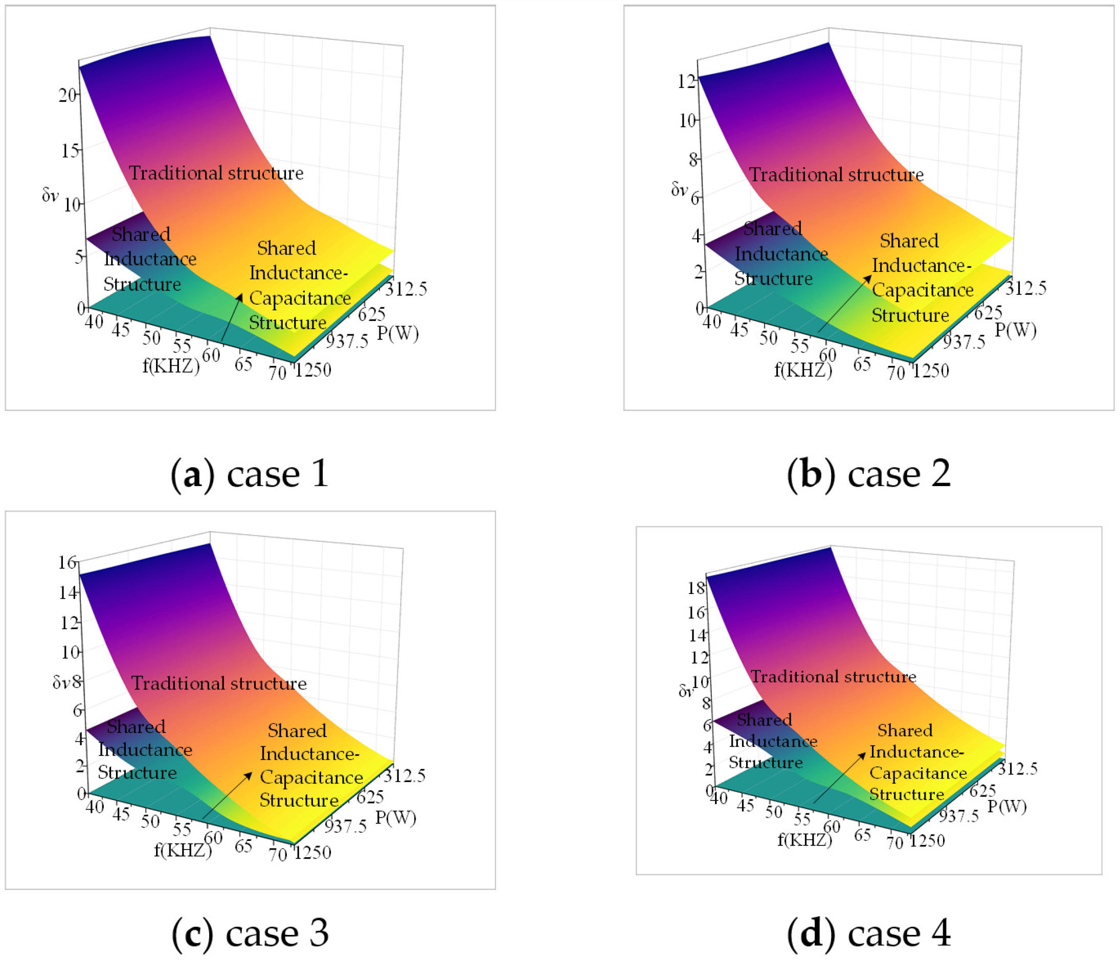
To demonstrate the advantages of the proposed interconnection-line shared inductance–capacitance structure in voltage equalization performance and its practical robustness to parameter tolerances, this section compares it with the traditional structure and the interconnection-line shared inductance structure. The four typical error combinations with the largest output voltage equalization errors from the 13 combinations in
Figure 8 are selected for comparison: Case 1 (a = 0.9, b = 0.9, c = 0.9), Case 2 (a = 0.9, b = 0.9, c = 1), Case 3 (a = 0.9, b = 1.1, c = 1.1), and Case 4 (a = 1, b = 0.9, c = 0.9). These four cases represent the most extreme parameter variation conditions and effectively validate the stability of the structure’s performance under extreme deviations.
Figure 9 shows the calculated output voltage equalization error
δv for the three structures under the parameters in
Table 2.
In Case 1 (a), with a switching frequency of 40 kHz and under half-load conditions, the voltage equalization error of the existing converter reaches 23%. The interconnection-line shared inductance structure has a voltage equalization error of 6.69%, while the proposed interconnection-line shared inductance–capacitance structure achieves complete voltage equalization between the phases. The above results show that the proposed passive voltage equalization structure not only significantly improves voltage equalization performance under harsh operating conditions across all error combinations but also maintains excellent voltage equalization in other conditions. This fully demonstrates the structure’s strong tolerance to the manufacturing tolerances of Lr, Cr and Lm, with robustness far superior to the traditional structure and the shared inductance structure. It greatly enhances the reliability of the converter in practical engineering applications.
3.6. Extension of the Proposed Shared Inductance–Capacitance Structure
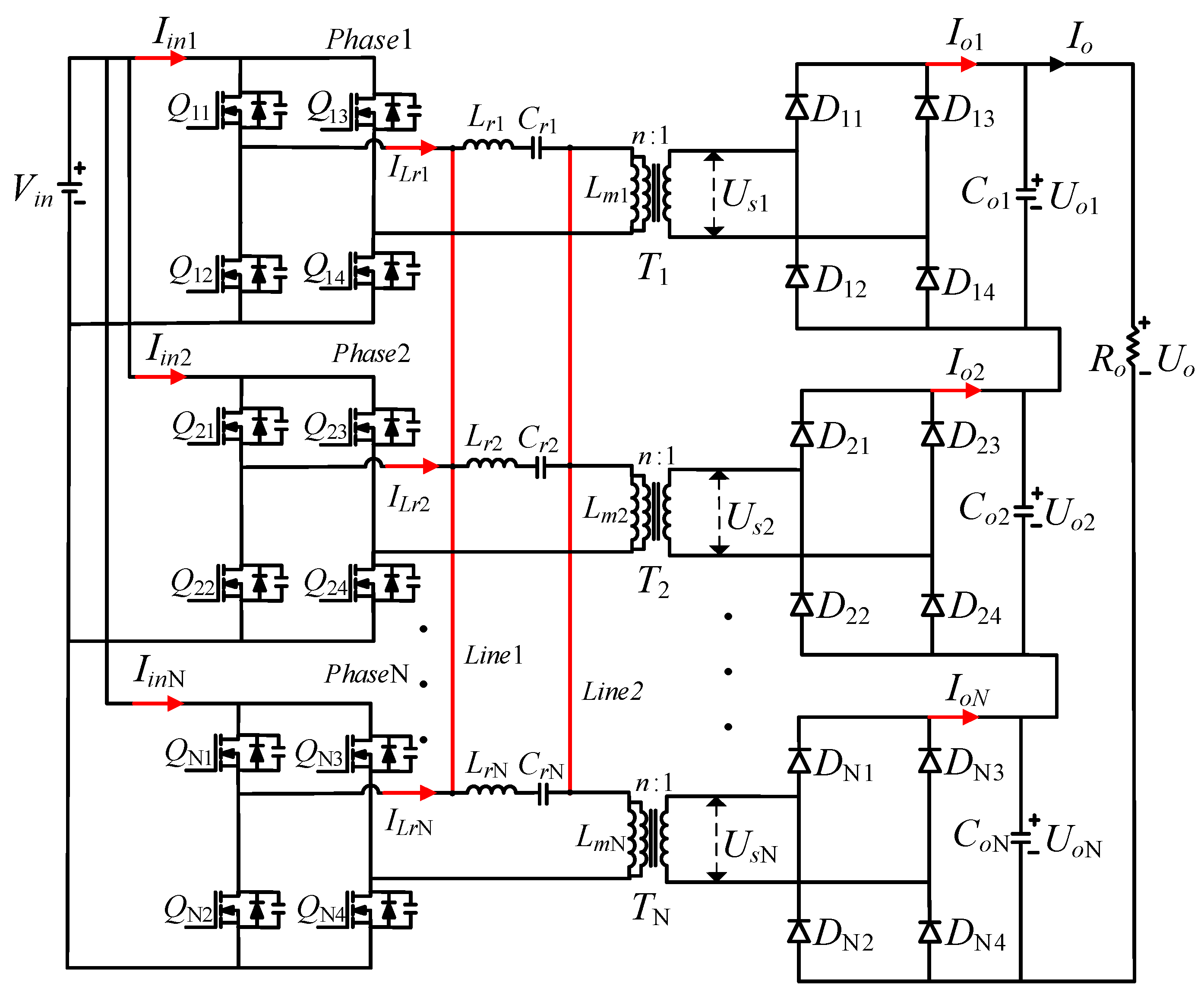
Building on the previous analysis of the two-phase voltage and current equalization characteristics, the extension of the proposed shared inductance–capacitance structure to multi-phase systems is further explored. The topology is shown in
Figure 10.
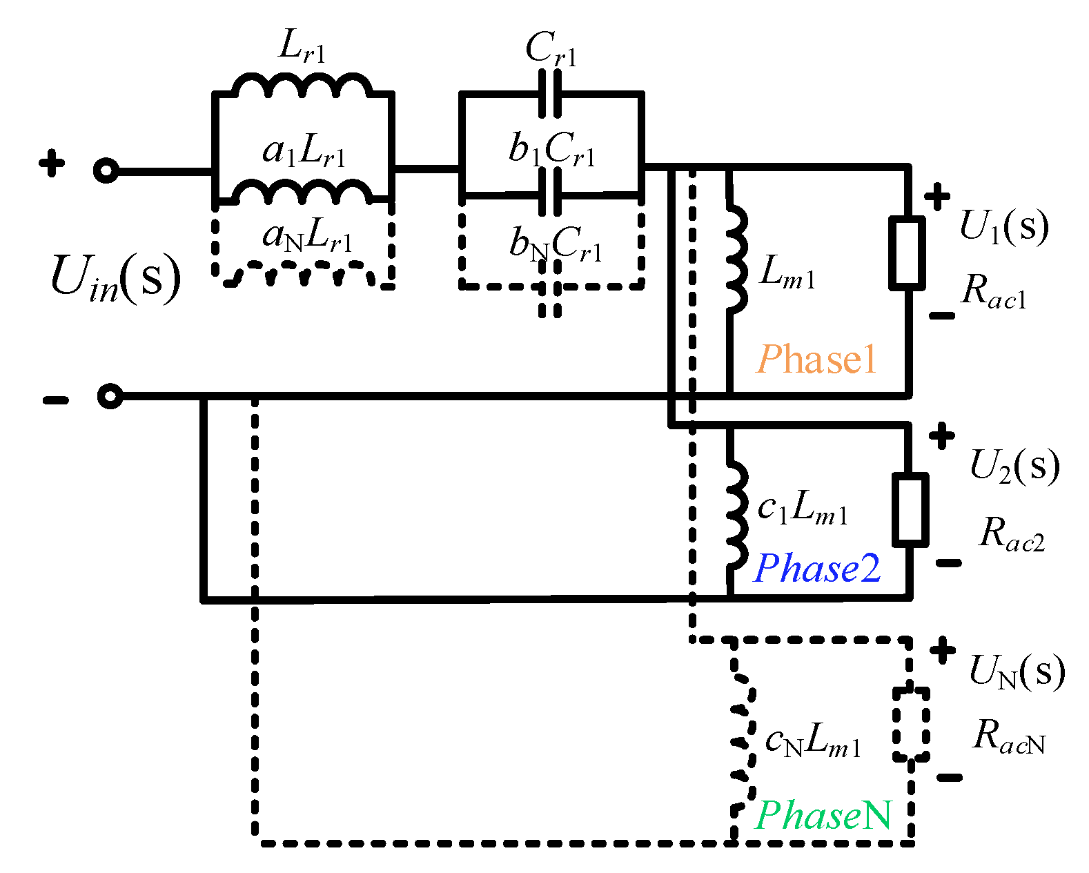
The fundamental harmonic equivalent circuit of the shared inductance–capacitance structure in an N-phase system is shown in
Figure 11.
The dashed lines in the figure represent the extended connections between modules. The resonant tank parameter error coefficients, aN, bN and cN, reflect the differences in resonant inductance, resonant capacitance, and magnetizing inductance between modules. Specifically, aN, bN and cN are within the range [0.9, 1.1]. In this way, the two-phase system can be extended to any number of modules.
As shown in
Figure 11, in the N-phase system, the resonant inductors and resonant capacitors of each phase are connected in parallel, forming a unified shared inductance–capacitance branch. The equivalent loads are connected in parallel, and the output voltage of each module is equal, improving current sharing and reducing circulating currents caused by one module bearing excessive power. This enhances the system’s efficiency and stability, reduces the interaction between resonant tanks, and prevents energy imbalance. A detailed simulation analysis will be provided in
Section 5.2 below.
6. Experimental Verification
6.1. Steady-State Experimental Result Validation
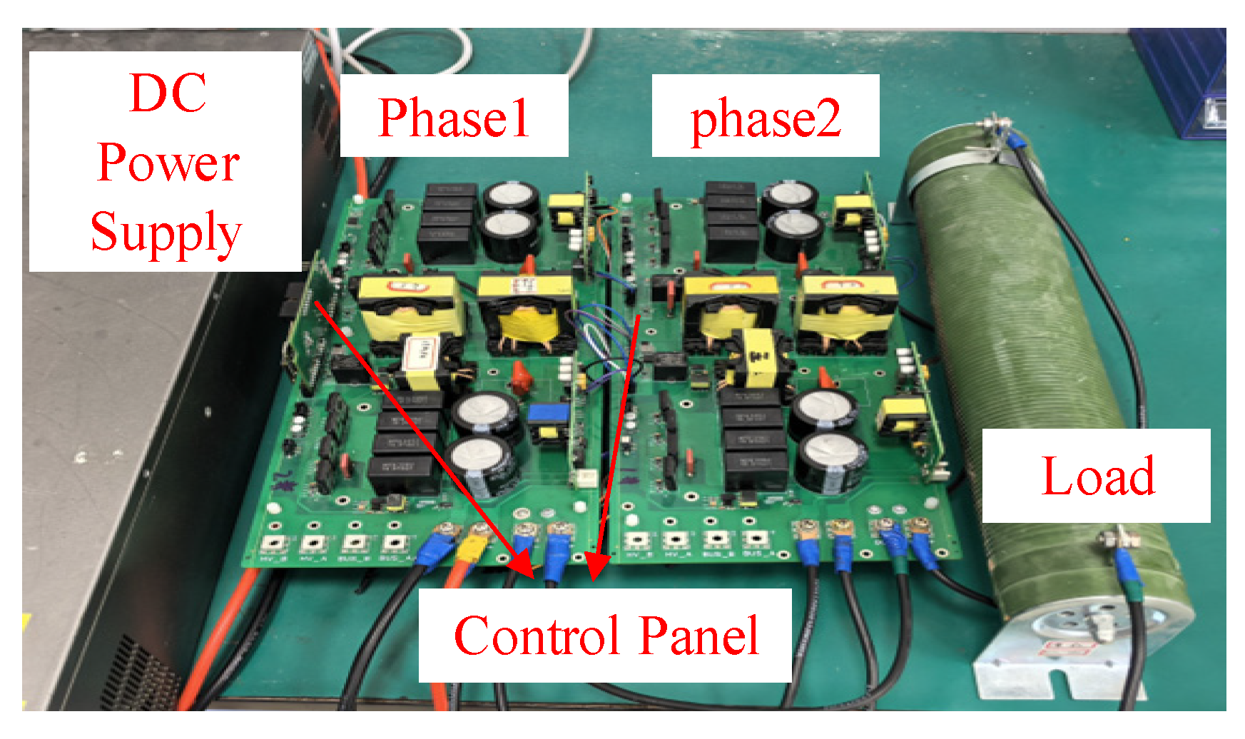
To verify the voltage and current equalization performance of the proposed structure, a 1.25 kW two-phase LLC resonant converter prototype was built, as shown in
Figure 18. The two-module LLC resonant converter shared the same control board, and the consistent timing of the power devices was ensured by sending unified driving signals. The actual parameters of the experimental platform prototype are shown in
Table 5.
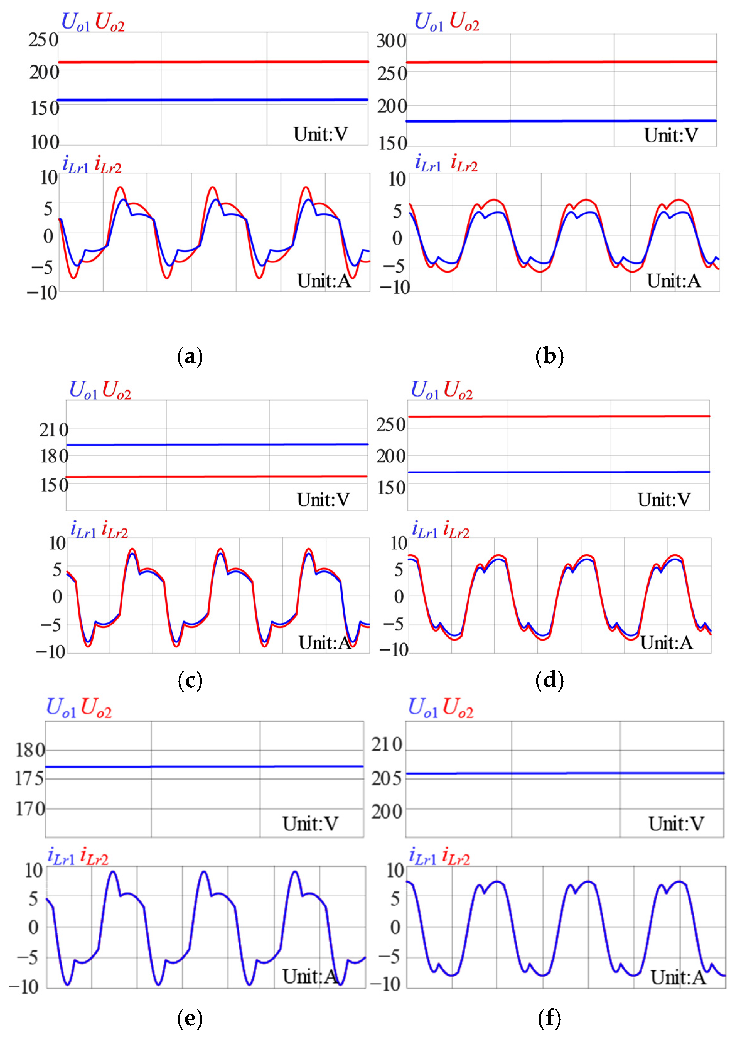
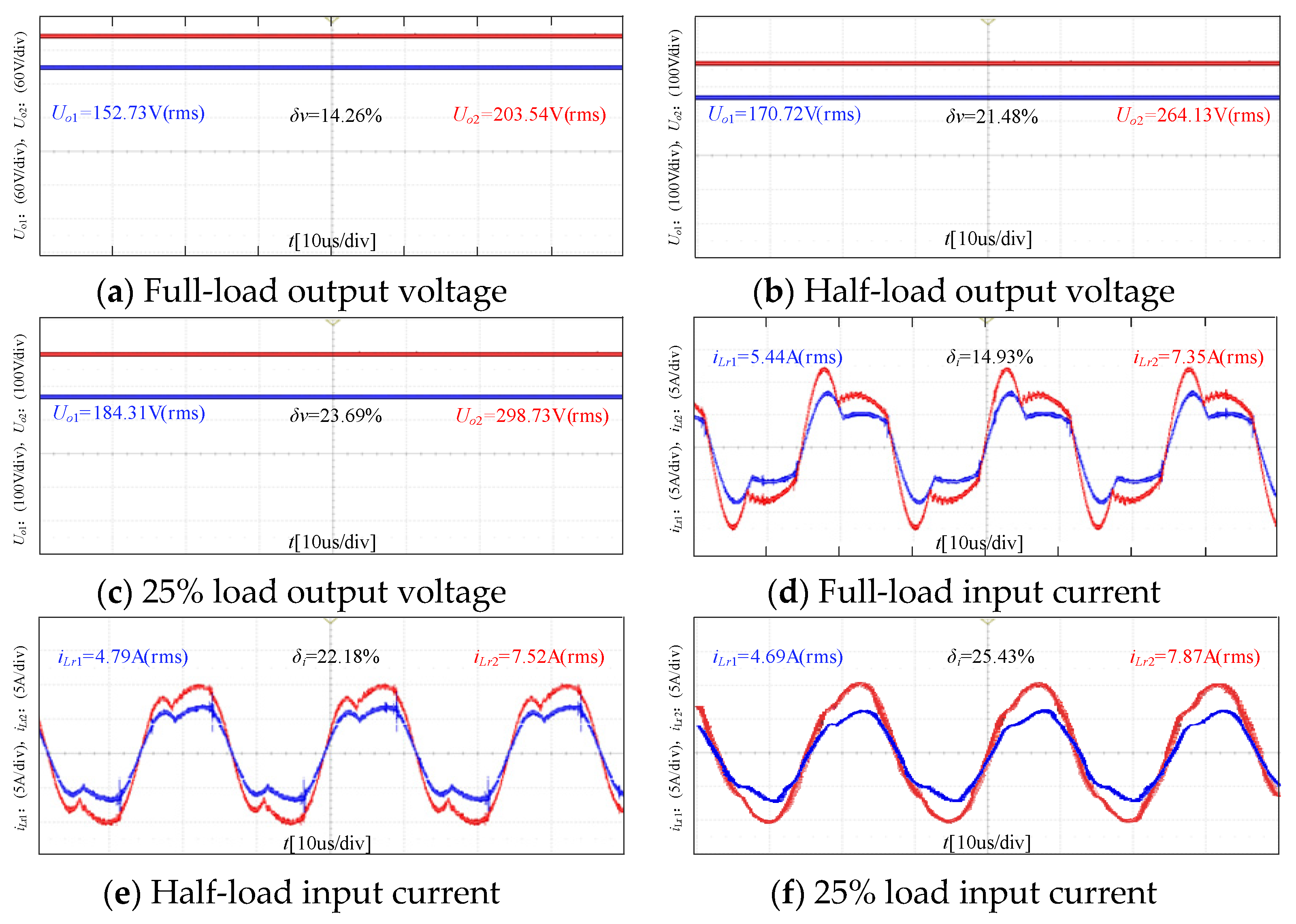
With an input voltage of 100 V, rated power of 1.25 kW, and switching frequency of 40 kHz,
Figure 19a–c present the output voltage waveforms of the traditional structure under full-load, half-load, and 25% load conditions, respectively.
Figure 19d–f show the corresponding input current waveforms.
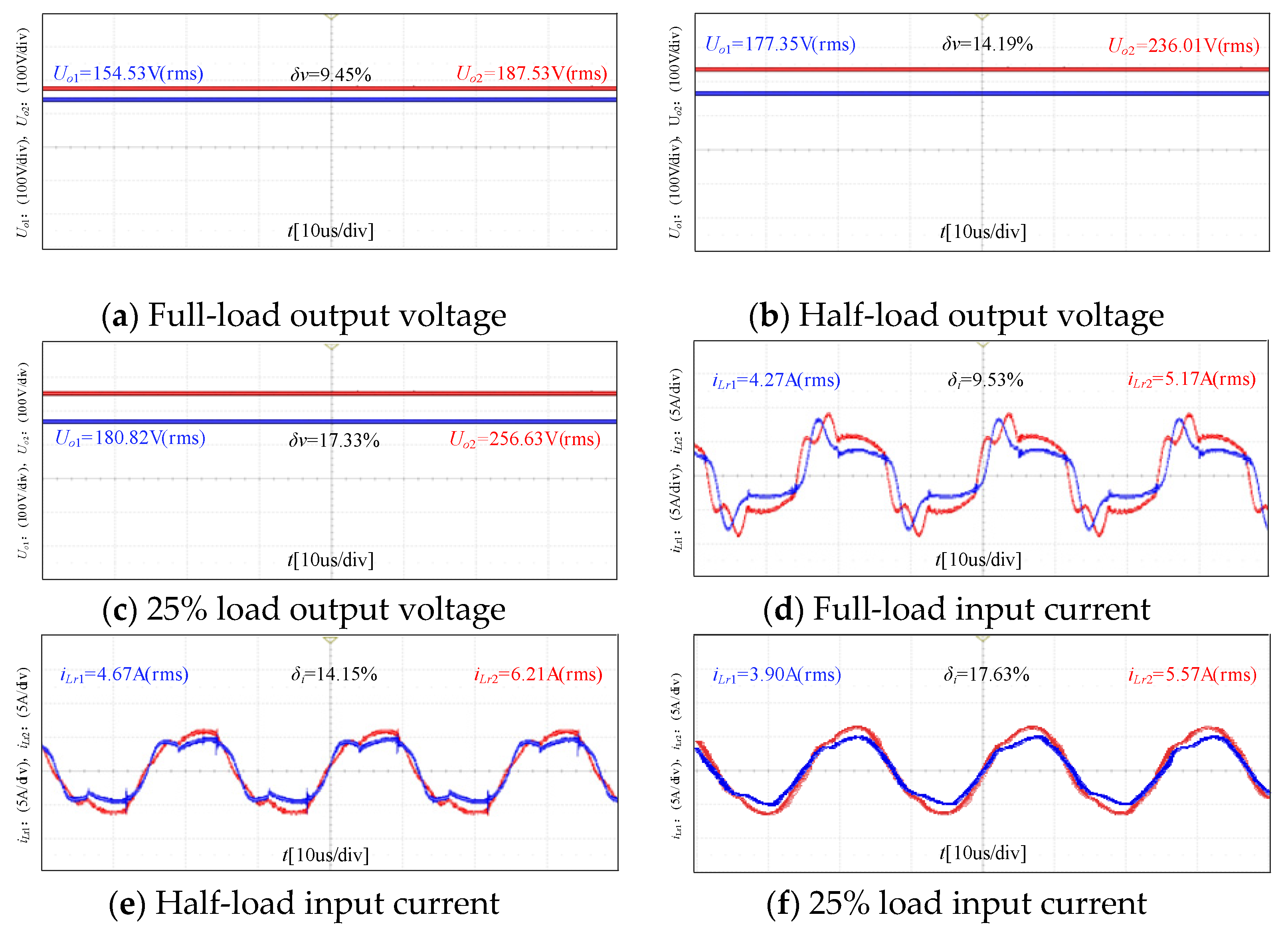
Figure 20a–c illustrate the output voltage waveforms of the interconnected shared-inductor structure under the same three load conditions, while
Figure 20d–f display the associated input current waveforms. Likewise,
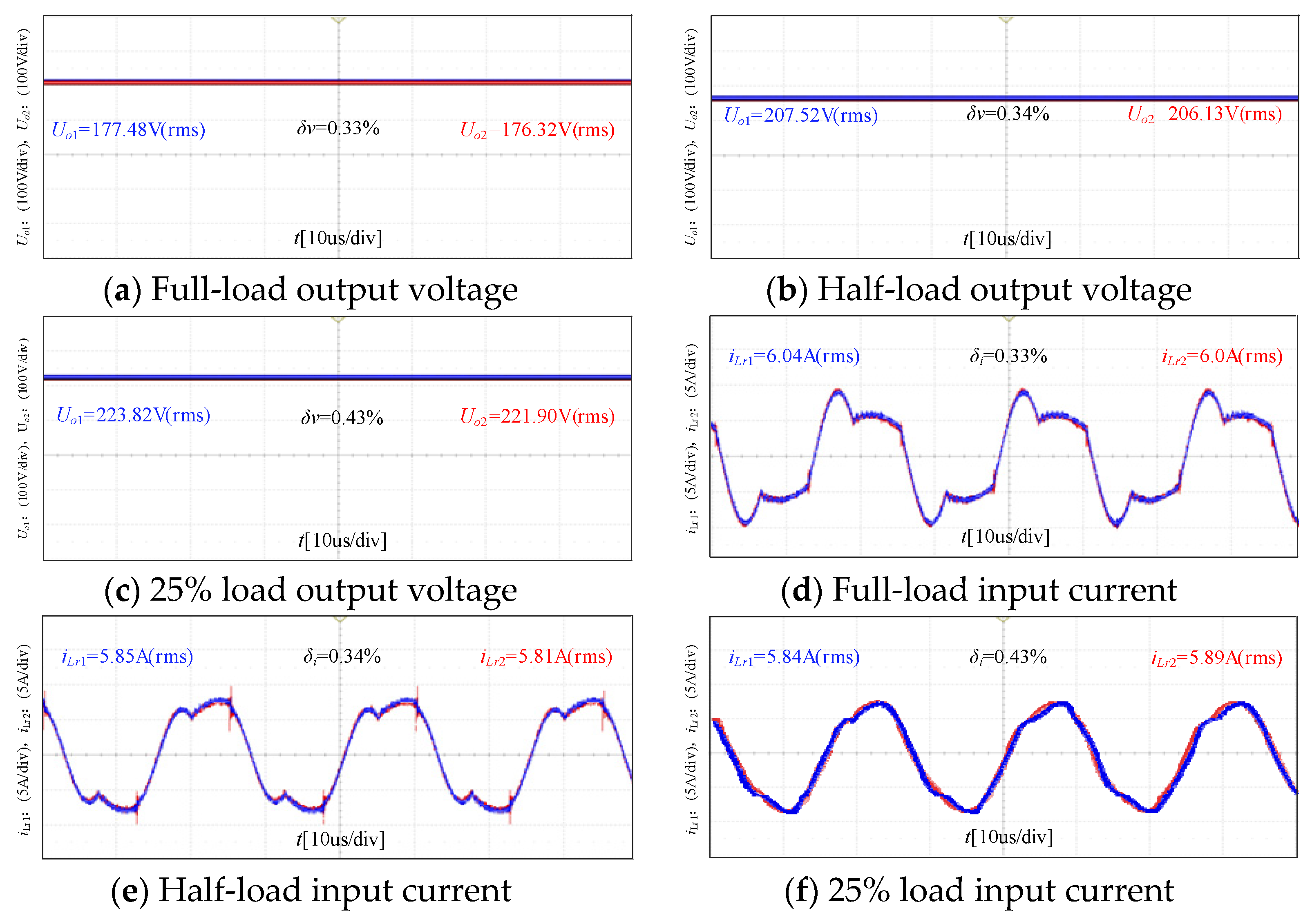
Figure 21a–c plot the output voltage waveforms of the proposed shared-inductor–capacitor structure under full-load, half-load, and 25% load conditions, and
Figure 21d–f show the corresponding input current waveforms.
From the experimental waveforms, the traditional structure exhibits two-phase output voltage errors of 14.26%, 21.48%, and 23.69% at full-load, half-load, and 25% load conditions, accompanied by input current errors of 14.93%, 22.18%, and 25.43%. For the interconnected shared inductor structure, the corresponding voltage errors are 9.45%, 14.19%, and 17.33%, while the current errors are 9.53%, 14.15%, and 17.63% under the same loading conditions. Strikingly, the proposed shared inductance–capacitance structure achieves ultra-low errors: only 0.33%, 0.34%, and 0.43% for both output voltage and input current throughout the entire load range. These results validate that the proposed structure realizes superior voltage and current balancing over the full operating range of the converter.
It is important to highlight that the proposed shared inductance–capacitance structure mitigates the issue of resonant current imbalance by establishing a unified shared inductance–capacitance network. This approach significantly reduces the resonant tank stress induced by current imbalance and prevents the additional losses associated with resonant current misbalance.
6.2. Dynamic Experimental Results
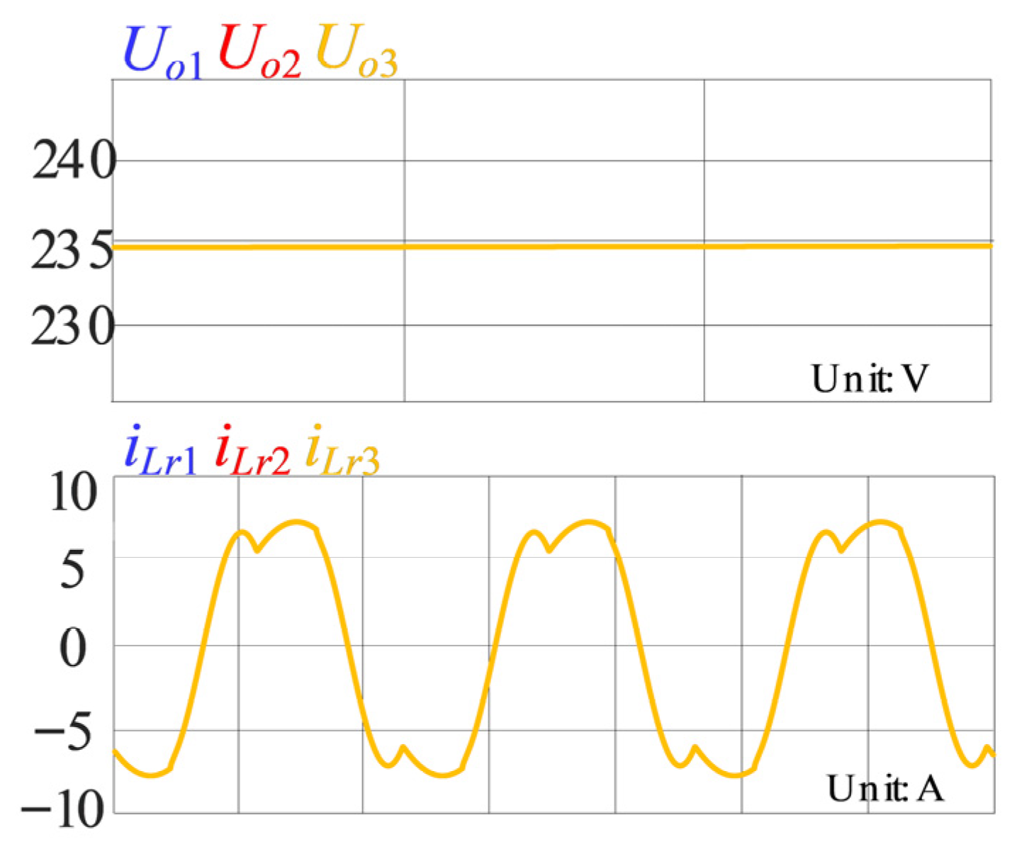
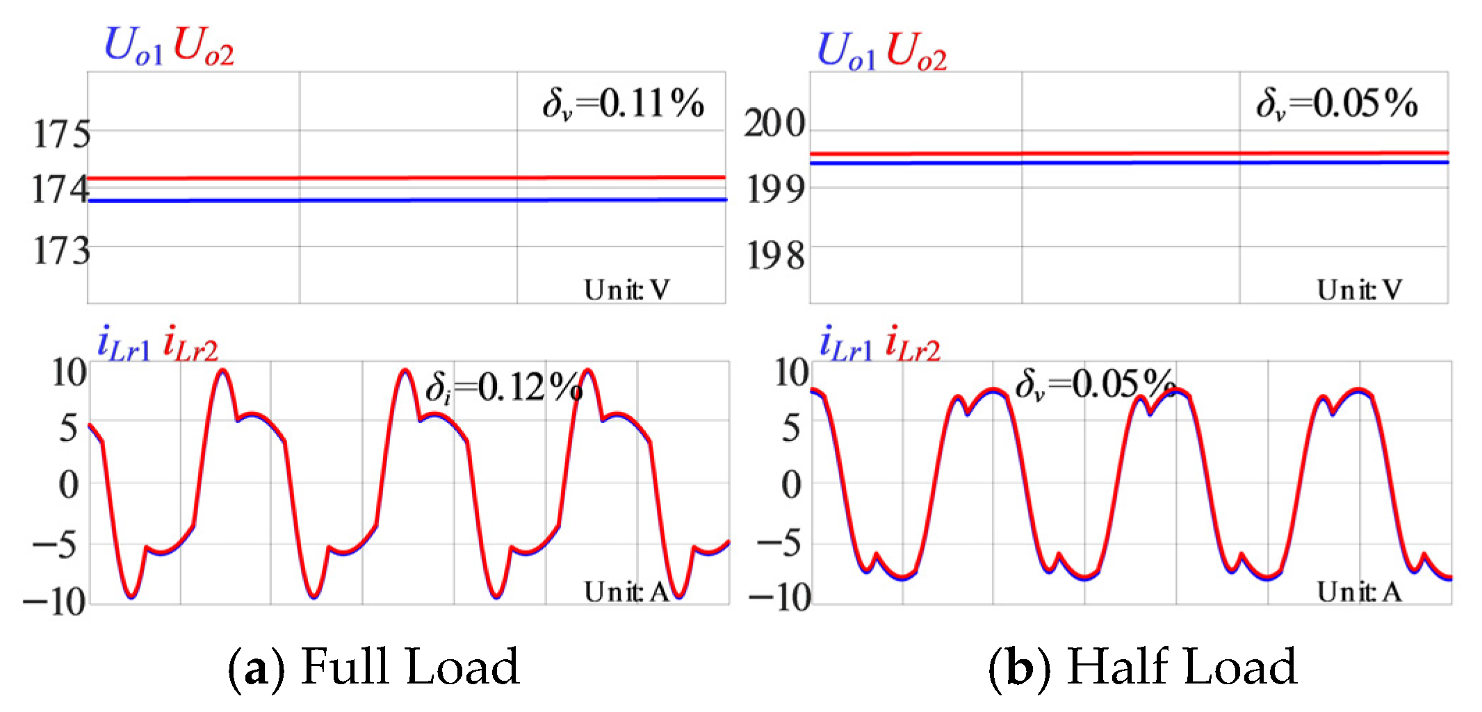
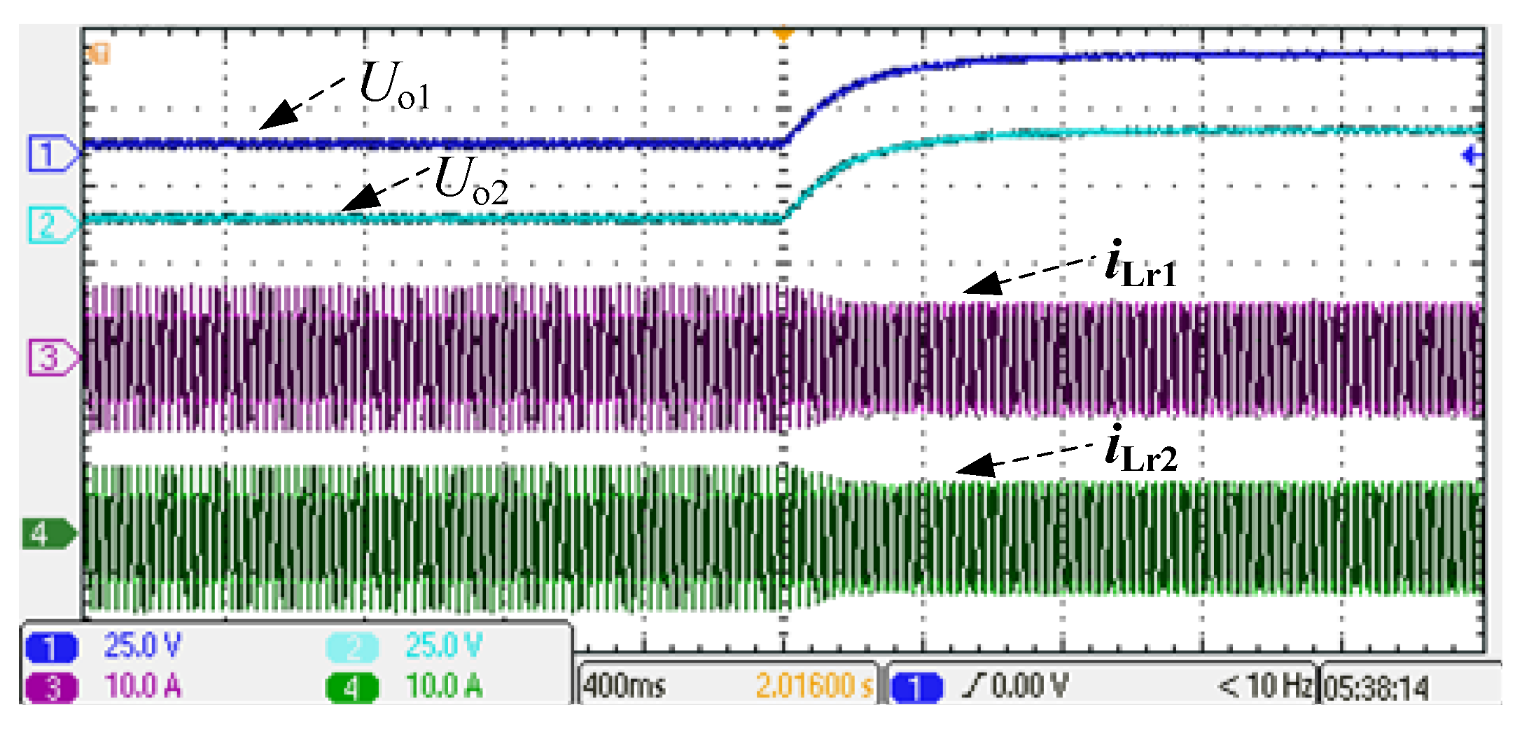
Figure 22 shows the experimental waveforms of the output voltage and resonant current for the two modules, corresponding to the full-load and half-load conditions of the proposed method.
As shown in
Figure 22, during the transition from full load to half load, the system is able to maintain stable output voltages
Uo1 and
Uo2, which fully demonstrates the excellent voltage-balancing capability of the proposed scheme during load switching. Meanwhile, during the switching process, the resonant currents
iLr1 and
iLr2 of the two modules remain highly synchronized, and the current distribution between the modules stays balanced, further proving that the system can maintain outstanding current-sharing characteristics under different load conditions. The system quickly stabilizes to the new operating state, indicating that the proposed solution has excellent responsiveness and stability under dynamic load variations, showcasing its voltage and current equalization ability in dynamic processes.
6.3. Comparison with Existing Solutions
The method proposed in this paper includes a unified shared inductance–capacitance branch using interconnection lines to achieve voltage and current equalization. The significant advantage or distinction of this method lies in its avoidance of complex control strategies and its modular characteristics. The comparison with existing active/passive equalization solutions is shown in
Table 6.
By comparison, the specific advantages of this solution are as follows:
- (1)
The ease of implementation and reliability of this method are superior to active balancing methods. For instance, droop control requires four current sensors and a complex control strategy, resulting in poor dynamic performance.
- (2)
Compared to other passive equalization methods, the proposed solution has lower complexity and features modularity, making it easier to scale to multi-phase systems as the system’s power capacity increases. This approach shortens the development cycle and reduces development costs.
7. Conclusions
To address the imbalances in output voltage and input current caused by parameter differences in the resonant tank components of input-parallel output-series LLC resonant converters, a new interconnection-line shared inductance–capacitance IPOS-type LLC resonant converter is proposed. This method achieves output voltage equalization and input current sharing between modules without the need for additional components or control strategies, significantly reducing system costs.
Furthermore, a new fundamental harmonic equivalent mathematical model is established for the proposed structure. Based on this model, the voltage and current equalization performance of the proposed converter is analyzed and compared with the voltage and current equalization characteristics of the traditional structure and interconnection-line shared inductance structure. Finally, the performance of a two-phase LLC resonant converter prototype is experimentally validated. The experimental results demonstrate that the proposed structure significantly reduces the output voltage and input current errors between the two phases under different resonant tank parameter variations. Additionally, this structure can be effectively extended to N-phase systems, providing an efficient voltage and current equalization solution for multi-module IPOS-type LLC resonant converters, with broad application prospects.
Future work will focus on in-depth investigations into the proposed shared inductance–capacitance structure, further evaluating its overall performance under non-ideal operating conditions. The planned tests and analysis include quantitatively assessing resonant tank voltage and current stress, system efficiency, and loss distribution tests. These endeavors will elucidate the impact of the proposed structure on voltage and current equalization accuracy, operational stability, and overall system performance.