1. Introduction
Multilevel converters (MLCs) have been extensively adopted in industrial power conversion systems due to their reduced semiconductor voltage stress, improved output waveform quality, and lower harmonic distortion, which collectively help relax filtering requirements and enhance overall system performance compared with conventional two-level converters [
1,
2,
3]. Among various MLC topologies, the five-level active neutral-point-clamped (5L-ANPC) converter has attracted increasing attention in recent years. It can synthesize multilevel voltages using a relatively small number of power switches and can exploit redundant switching states under appropriate modulation to regulate and balance the split DC-link capacitor voltages, thereby offering a favorable tradeoff between performance and implementation complexity [
4,
5,
6,
7]. From a system-integration perspective, ANPC-based solutions typically do not require multiple isolated DC sources as in cascaded H-bridge (CHB) converters, which simplifies front-end power supply design; moreover, compared with flying-capacitor converters (FCCs) and modular multilevel converters (MMCs), ANPC converters generally employ fewer and/or smaller passive energy-storage components, which is beneficial for increasing power density and reducing system volume and engineering effort [
8,
9,
10,
11,
12,
13].
In addition to these general advantages, the 5L-ANPC topology is particularly attractive for the present study because its redundant switching states and small-vector allocation flexibility make it possible to achieve neutral-point regulation and DC-side power redistribution without introducing additional auxiliary hardware.
Nevertheless, DC-link capacitor-voltage regulation and neutral-point (NP) potential balancing remain critical to the stable operation of 5L-ANPC converters. Sustained NP deviation may impose excessive voltage stress on specific devices, degrade conversion efficiency, and deteriorate output voltage/current waveforms, resulting in a pronounced increase in total harmonic distortion (THD) and, consequently, reduced reliability and grid-interfacing performance.
To address the NP balancing problem in 5L-ANPC converters, existing studies have mainly investigated modulation optimization, topology enhancements, model predictive control (MPC), and other balancing schemes.
From the modulation perspective, carrier-based techniques are widely used due to their simplicity and ease of implementation. For example, optimized carrier-based PWM has been employed for NP regulation; phase-shift PWM (PSPWM) exhibits an inherent tendency to balance certain capacitor voltages, yet challenges persist in balancing specific high-side capacitors [
14]. Carrier-overlapping PWM (COPWM) has also been proposed to mitigate NP voltage imbalance in five-level NPC inverters, where a staged balancing procedure is used to equalize multiple DC-side capacitor voltages [
4]. In addition, discontinuous PWM (DPWM) has been introduced to single-phase 5L-ANPC converters to reduce switching losses while achieving NP and capacitor-voltage balancing [
15].
From the space-vector viewpoint, space-vector modulation (SVM/SVPWM) is attractive due to its high DC-bus utilization and strong modulation flexibility. Lookup-table-based SVPWM strategies have been reported, where the operating region is partitioned according to the direction of the phase current and different vector sequences are selected to regulate the NP potential [
16]. Prior work also indicates that SVM can achieve lower capacitor-voltage ripple and reduced current harmonics compared with sinusoidal PWM (SPWM) [
17]. For more complex topologies where DC NP voltage and floating-capacitor voltages are coupled, improved SVM schemes incorporating capacitor-voltage control have been developed to enhance multi-objective balancing capability [
18]. In the three-level NPC domain, zero-sequence injection and duty-ratio decomposition methods have been adopted to achieve fast NP balancing with a low computational burden, providing useful references for higher-level modulation design [
19,
20].
From the topology perspective, various ANPC derivatives with self-balancing characteristics or voltage-boost capability have been proposed to reduce balancing difficulty and improve device stress distribution. Representative examples include an improved self-balancing 5L-ANPC topology intended to mitigate voltage balancing issues associated with series devices and large voltage transitions [
21], as well as five-level switched-capacitor ANPC inverters featuring step-up capability, low device voltage stress, and floating-capacitor balancing without auxiliary circuits or sensors [
22]. To address limited voltage gain or common-mode voltage concerns, alternative structures such as split-point cross-clamped and common-ground boost-type ANPC topologies have been reported to improve DC-bus utilization and electromagnetic compatibility (EMC) performance [
23,
24].
From the control perspective, MPC has demonstrated strong potential for multilevel converters because it can simultaneously consider current tracking, capacitor-voltage balancing, common-mode voltage suppression, and switching-loss constraints in a unified framework. For instance, OSS-based MPC has been applied to single-phase grid-connected NPC-type converters to coordinate grid-current tracking and capacitor-voltage balancing [
25]. Other studies further incorporate small-vector group selection and tailored cost functions to achieve multi-objective optimization [
26]. In this work, a small-vector regulation approach is adopted by introducing the small-vector duty factor,
n, to regulate the NP potential, which features a simple implementation mechanism and effective balancing performance [
27].
Despite the aforementioned progress, as application scenarios evolve from conventional inverter operation toward rectification, bidirectional power conversion, and DC-side integration of diverse loads, NP regulation in complex operating conditions still faces new constraints and challenges. On the one hand, the number of redundant states increases markedly in higher-level topologies, and the associated vector selection and dwell-time computation become more involved, making fast and accurate NP control under dynamic conditions more difficult. On the other hand, many existing methods primarily focus on “eliminating NP deviation”, while the mechanism by which NP deviation induces vector synthesis errors, waveform distortion, and stability deterioration under practical operating scenarios has not been sufficiently characterized. More importantly, most studies are built upon the implicit assumption of symmetric split-capacitor voltages and do not fully exploit a key structural advantage of the 5L-ANPC converter under rectifier operation—namely, that its DC side can provide positive, neutral, and negative DC buses. This feature enables the upper and lower capacitors to interface independently with DC loads of different types and ratings, which is highly relevant to distributed generation, energy storage systems, and integrated energy routing applications. However, when the DC-side load power mismatch becomes significant, unequal discharge rates of the upper and lower capacitors can drive sustained NP drift. Even if the small-vector duty factor, n, is pushed to its extreme limits (n = 0 or n = 1), NP balance may still be unattainable because the load mismatch exceeds the compensation capability inherently available through small-vector regulation.
To tackle these issues, this paper conducts the following investigations. In this work, the term “modulation optimization” specifically refers to a neutral-point-deviation-adaptive SVPWM strategy for the 5L-ANPC converter under DC-side unbalanced-load conditions. This optimization consists of dynamic sector boundary reconstruction, dwell-time correction based on the actual split-capacitor voltages, and optimized small-vector allocation through the adjustable duty factor, n.
Meanwhile, the term “load power boundary condition” refers to the analytically derived feasible range of the upper-to-lower average load power ratio under which the neutral-point potential remains controllable through small-vector regulation without additional auxiliary hardware. This boundary is jointly determined by the reference voltage magnitude, Uref (or modulation index, m), and the small-vector duty factor, n.
First, an improved SVPWM scheme is developed for operating conditions with dynamic NP deviation. By optimizing sector boundary partitioning and revising the volt–second balance-based dwell-time calculation, the proposed strategy allows vector selection and dwell times to reflect real-time variations in the split-capacitor voltages, thereby suppressing waveform distortion during the balancing process and improving modulation accuracy.
Second, a unified “DC-side average-power feasibility (boundary) model and power allocation strategy” is established to characterize the admissible operating range for rectifier operation with DC-side unbalanced loads. Based on power-transfer mechanisms, an energy-interaction model between the split capacitors and their respective loads is formulated. Over a fundamental-cycle timescale, the influences of space-vector dwell times in different sectors on the average power of the upper and lower branches are analytically evaluated. This leads to a functional relationship between the average branch power ratio; the reference voltage-vector magnitude, Uref; and the small-vector duty factor, n, from which a boundary expression is derived to quantify the range in which the NP potential remains controllable under the given modulation strategy. Within this framework, for resistive-load scenarios, the effects of the load power ratio on charge/discharge paths and NP evolution are analyzed to clarify the mechanism of NP drift caused by power imbalance and to identify the region where dynamic NP balancing can be maintained. For battery-type loads with voltage-source characteristics, whose terminal voltages are approximately constrained near rated values and thus cannot be symmetrized solely through NP regulation, the control objective is extended from voltage symmetry to power/current allocation. A mapping between n and the average branch power (or charging/discharging current) is established within the feasibility region, and an online power allocation algorithm is developed to achieve controllable and symmetric battery-branch currents under rated-voltage constraints.
Furthermore, focusing on resistive-load integration, systematic analyses are performed across different load power ratios to elucidate the intrinsic mechanism of NP drift and to confirm the stable regulation capability within the derived boundary region.
Finally, experimental validation is carried out on an Hardware-in-the-loop experiments were conducted on an OPAL-RT OP5707-based platform running RT-LAB v2021.2.0.244. where both single-phase and three-phase 5L-ANPC systems are implemented. The derived average-power boundary condition for resistive loads is verified in the single-phase system, while the proposed modulation strategy and battery-load power-sharing control are further validated in the three-phase system.
2. Operating Principle of the Three-Phase Five-Level ANPC Converter
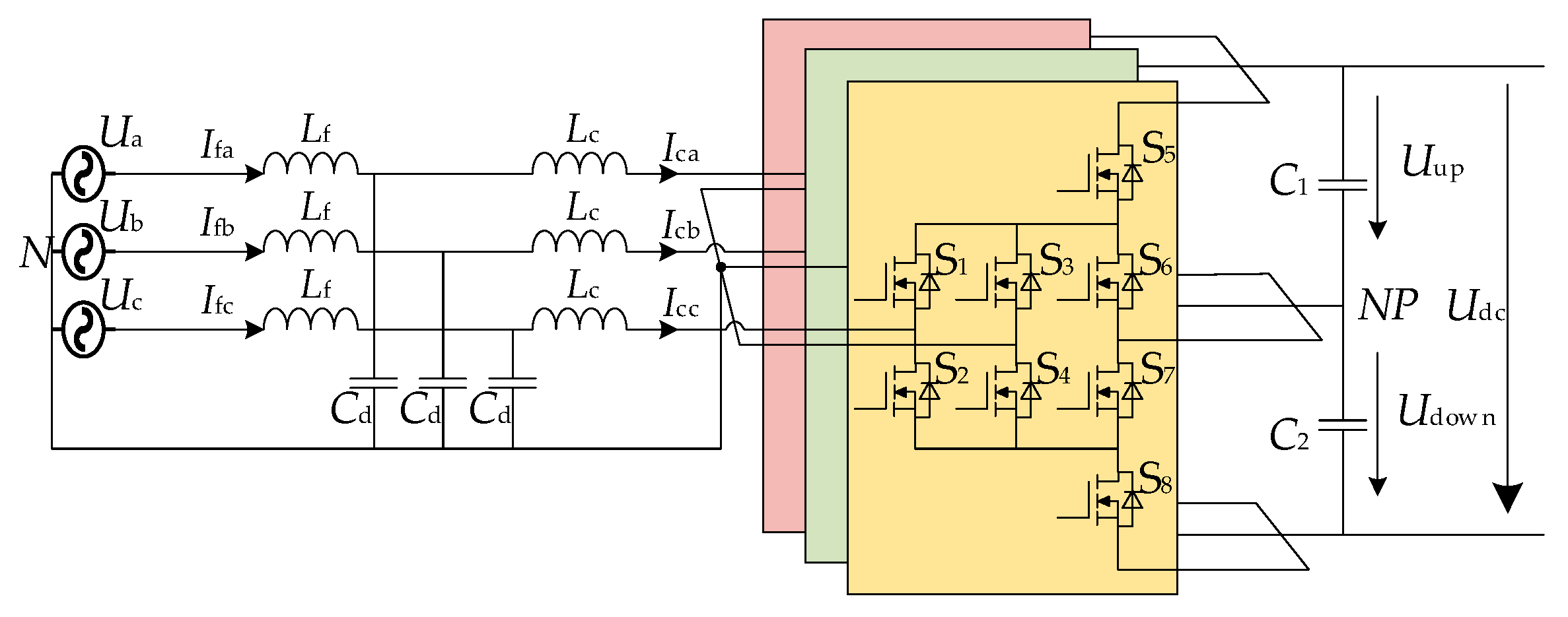
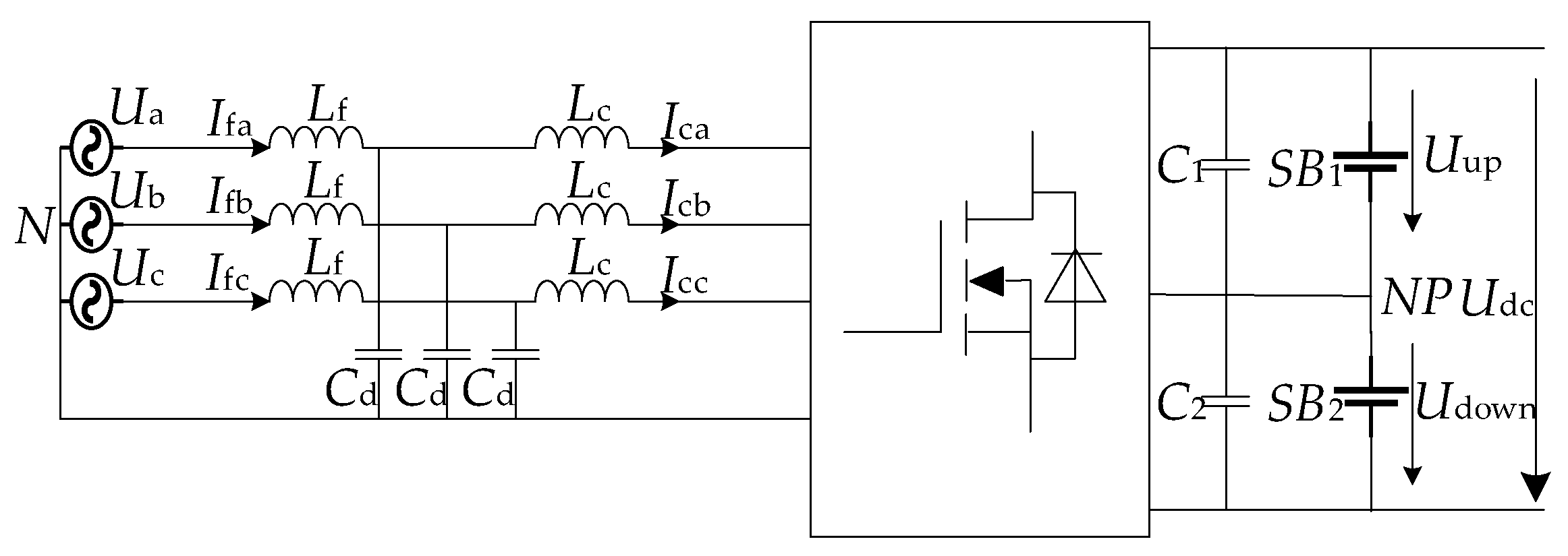
The overall configuration of the three-phase 5L-ANPC converter is shown in
Figure 1.
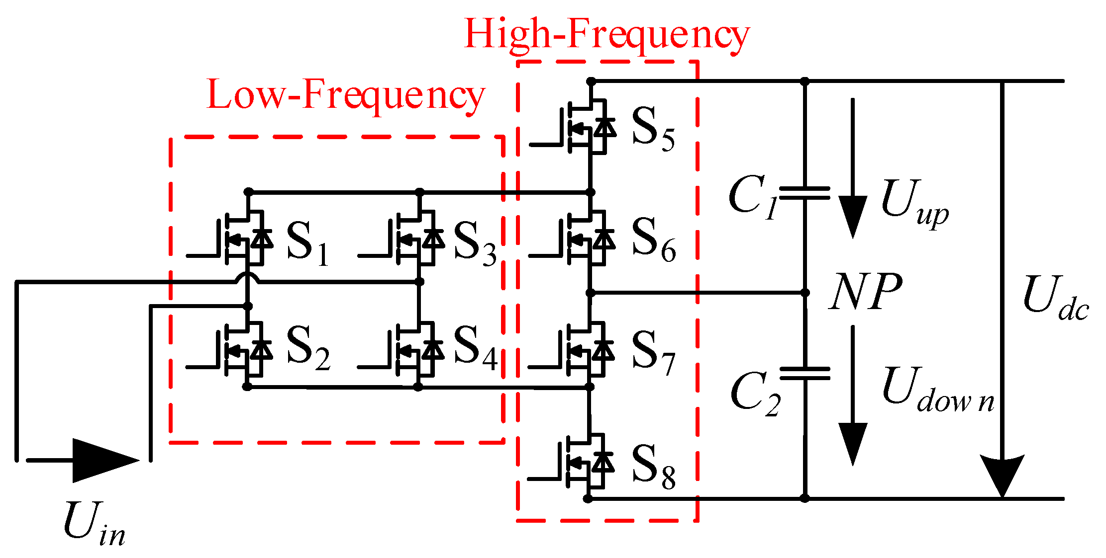
On the AC side, the system is connected in a three-phase four-wire scheme, i.e., the A/B/C phase conductors share a common neutral conductor, N. On the DC side, the split DC-link capacitors form three DC buses (positive bus, midpoint bus, and negative bus), and the three phase-leg power units are connected in parallel to these DC buses, thereby sharing the same DC-link and midpoint. For clarity, the switching states, modulation scheme, and neutral-point regulation mechanism are described using a single-phase power unit as an example, as depicted in
Figure 2.
The single-phase unit adopts a hybrid-device and dual-frequency modulation approach: switches S1–S4 constitute a low-frequency H-bridge for AC polarity commutation, whereas switches S5–S8 form a high-frequency modulation stage responsible for voltage-level synthesis and power processing. It should be noted that the three-phase topology can be viewed as a DC-side parallel extension of the single-phase unit, while the AC-side interface is realized via the shared neutral conductor, N.
The switching states of the single-phase 5L-ANPC converter are listed in
Table 1.
During the positive half-cycle, mode P corresponds to an outer voltage vector and produces the DC-bus voltage, Udc, between the positive and negative DC rails. Modes HP+ and HP− correspond to a pair of redundant positive small voltage vectors, where HP+ outputs the upper split-capacitor voltage, Uup, and HP− outputs the lower split-capacitor voltage, Udown, on the DC side. In addition, modes OL+ and OL− form redundant zero vectors, both yielding a zero-output voltage.
During the negative half-cycle, mode N corresponds to an outer voltage vector and produces −Udc. Modes HN+ and HN− correspond to a pair of redundant negative small voltage vectors, where HN+ outputs −Uup and HN− outputs −Udown (Udc = Uup + Udown).
With eight distinct switching-state combinations, the proposed topology can generate five different voltage levels.
As can be observed from
Table 1 and
Figure 2, under rectifier operation, the switches S1–S2 and S3–S4 in the low-frequency H-bridge are driven in a complementary manner to rectify the input AC voltage and control the polarity commutation, thereby producing a three-level DC voltage waveform. Meanwhile, the high-frequency DC/DC modulation stage employs complementary switching for S5–S6 and S7–S8. By means of high-frequency modulation, this stage performs voltage-level synthesis and power/energy distribution, resulting in a stable DC-side output voltage with reduced ripple and improved smoothness.
3. Misclassification Mechanism and Volt–Second Mismatch Analysis of Conventional SVPWM Under Neutral-Point Potential Deviation
In five-level converters, SVPWM is not only employed for accurate reference vector synthesis but also serves as an effective neutral-point regulation framework by exploiting redundant switching states. Specifically, multiple switching combinations can generate an identical output voltage vector while producing different neutral-point current injection characteristics; hence, the neutral-point voltage (or split-capacitor voltages) can be regulated without altering the commanded output vector. Existing SVPWM-based balancing approaches mainly rely on (i) state/sequence selection laws that map the current direction and operating region to “raise/lower” neutral-point tendencies (often implemented via rule sets or look-up tables) and (ii) zero-vector (and redundant small-vector) dwell-time allocation, where the average neutral-point current over a switching period is shaped to suppress capacitor-voltage drift and ripple [
27]. These methods are typically augmented with a capacitor-voltage feedback loop, which updates dwell times or candidate sequences online to improve balancing capability under operating transients while maintaining acceptable current harmonic performance [
14].
Motivated by the above, this paper adopts a symmetric five-segment SVPWM in which the synthesized sequence starts and ends with small vectors. The resulting pattern enforces time symmetry and favors single-switch transitions, thereby reducing commutation events and mitigating vector-discontinuity-induced distortion around sector boundaries. More importantly, the structured sequence provides a consistent modulation basis for subsequent enhancements under neutral-point deviation and DC-side load asymmetry, including sector-decision correction, volt–second balance compensation, and power-sharing coordination.
The modulation signal used in the 5L-ANPC converter is defined as the reference voltage vector,
Uref, which is expressed as
where
ω is the grid angular frequency and
m is the modulation index, defined as
where
Uac denotes the RMS value of the AC-side phase voltage.
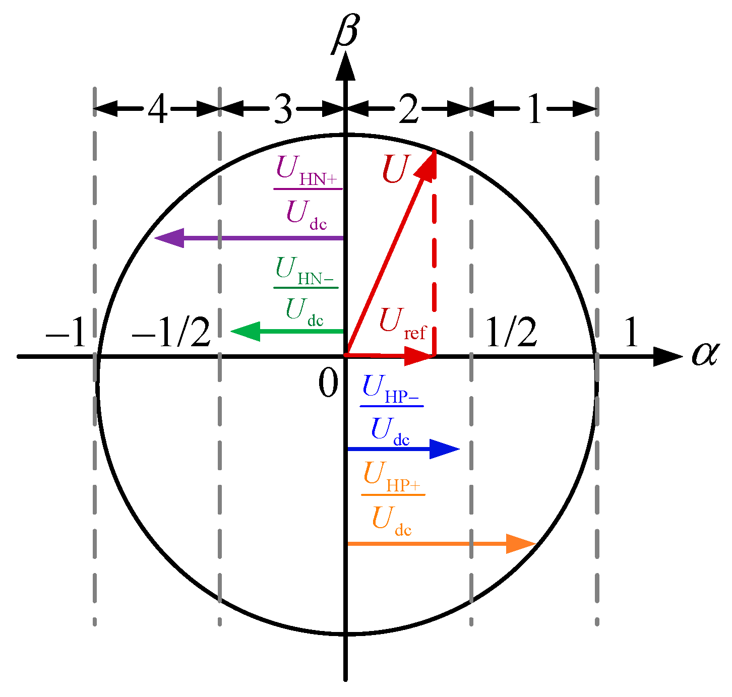
To date, the sector partitioning of the 5L-ANPC converter has typically been established under the ideal assumption that the DC-side neutral-point potential is balanced, i.e., the split-capacitor voltages satisfy
Uup =
Udown =
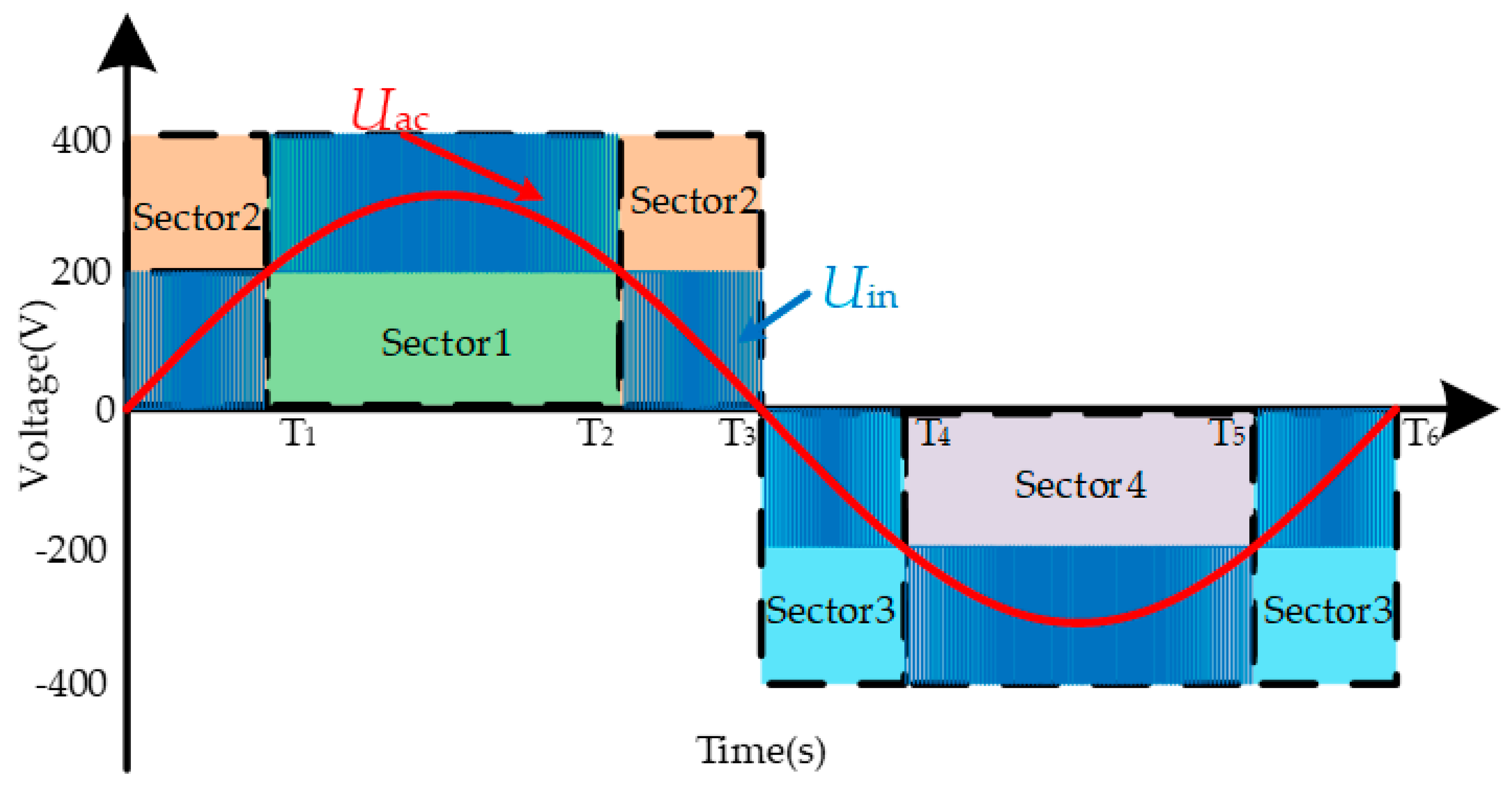
Udc/2. Under this assumption, the voltage-vector magnitudes are used to divide the space-vector plane into four fixed regions, as illustrated in
Figure 3.
However, when the neutral-point potential deviates from its balanced condition, the above sector partitioning becomes inaccurate. Since the split-capacitor voltages no longer equally divide the DC-bus voltage, the boundaries between Sectors 1 and 2 and between Sectors 3 and 4 should not remain fixed at ±0.5; instead, they must be dynamically updated according to the actual ratios of the capacitor voltages to the DC-bus voltage.
If the conventional “ideal” sector boundaries are still applied, a reference voltage vector that should fall in Sector 2 or Sector 3 may be misclassified into Sector 1 or Sector 4. This misclassification leads to improper vector selection, causing the synthesized voltage vector to deviate from the reference and violating the volt–second balance constraint. Consequently, waveform distortion can appear on the AC side during the neutral-point regulation process.
In addition to sector misclassification, the conventional SVPWM also relies on the symmetric small-vector magnitude assumption to derive the volt–second balance equations, which no longer hold under neutral-point imbalance. Taking the positive half-cycle as an example, the corresponding relationship is given by
where
UP,
UHP+,
UHP−, and
UOL+ denote the output voltages corresponding to the above modes;
TP,
THP+,
THP−, and
TOL+ are the associated vector dwell times; and
Tc is the carrier period.
Table 2 lists the selected switching vectors and the corresponding switching sequences for each sector under different operating conditions, and it also indicates which vectors require extended dwell times when the neutral-point potential is unbalanced; this information provides a direct guideline for dwell-time adjustment to regulate the neutral-point voltage while preserving the desired output-vector synthesis. Moreover, by explicitly identifying the “priority” vectors for compensation in each sector,
Table 2 facilitates a consistent implementation of the balancing algorithm across operating regions and improves the reproducibility of the modulation procedure.
When the neutral-point potential deviates, the split DC-link capacitor voltages are no longer equal in magnitude. Under this condition, the dwell times computed from the conventional SVPWM formulation—derived under the capacitor-voltage symmetry assumption—cannot satisfy the volt–second balance constraint of the actual space vectors. Consequently, the synthesized voltage vector departs from the reference vector and the resulting tracking error accumulates over consecutive PWM periods, which manifests as output-voltage distortion, increased AC-side current harmonics, and a substantially reduced effective regulation range of redundant small vectors for neutral-point control. Therefore, under neutral-point imbalance, conventional SVPWM is simultaneously constrained by sector-decision inaccuracy and volt–second mismatch, making it difficult to ensure correct vector selection and accurate dwell-time allocation.
Moreover, in rectifier operation, the 5L-ANPC converter provides a structural advantage by exposing the positive, neutral, and negative DC buses, enabling the upper and lower DC-link capacitors to interface with DC loads of different voltage levels or power ratings. However, under such DC-side load asymmetry, the power demand and charge/discharge paths of the upper and lower branches differ significantly, which tends to aggravate the neutral-point deviation. In this operating scenario, conventional SVPWM still relies on the ideal assumption Uup = Udown, such that the assumed small-vector magnitudes, sector boundaries, and volt–second balance equations become inconsistent with the real operating conditions. As a result, effective neutral-point regulation becomes even more challenging. In other words, for ANPC converters exploiting the “three-DC-bus” capability to supply asymmetric DC loads, conventional SVPWM may no longer meet the requirements for neutral-point potential control.
Accordingly, the key limitations of conventional SVPWM under asymmetric DC-load conditions can be summarized as follows:
Challenge 1: Limited neutral-point controllability under load asymmetry.
The 5L-ANPC converter allows the upper and lower DC-link capacitors to supply DC loads with different power ratings. When the loads are asymmetric, the capacitor charge/discharge rates become substantially different. Conventional SVPWM—designed under the symmetry assumption—cannot adequately accommodate this operating condition, leading to persistent neutral-point drift and difficulty in restoring balance.
Challenge 2: Degraded vector synthesis accuracy, resulting in AC-side current distortion.
Neutral-point deviation changes the actual magnitudes of the small vectors and shifts the effective sector boundaries in the space-vector plane. If the conventional fixed boundaries (e.g., ±0.5) are still used, the reference vector can be misclassified into an incorrect sector, causing improper basic-vector selection. Meanwhile, because the positive/negative small vectors are no longer symmetric, the conventional volt–second balance equations become invalid and the computed dwell times no longer match the required values. The combined effects of sector misclassification and volt–second mismatch force the synthesized vector to deviate from the reference, thereby introducing AC-side current distortion and increasing harmonic contents.
4. Neutral-Point-Deviation-Adaptive SVPWM via Sector-Boundary Reconstruction and Dwell-Time Correction
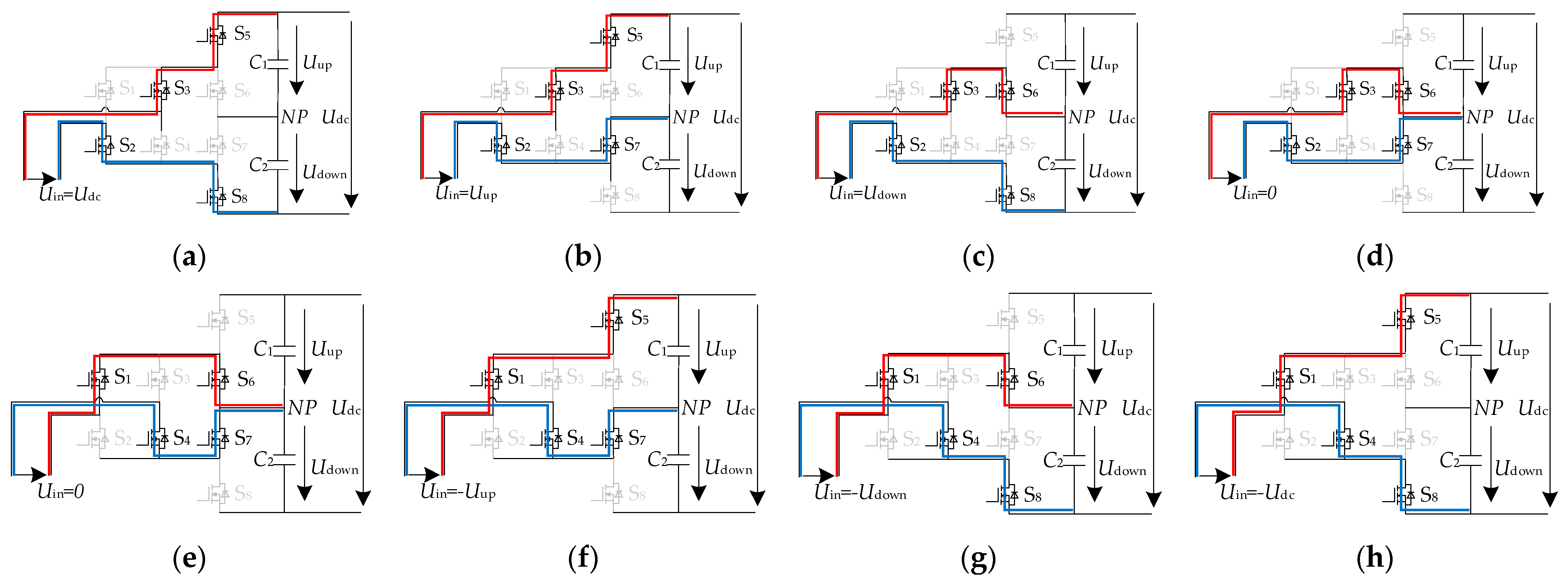
The output voltages and current conduction paths of the 5L-ANPC converter under different voltage vectors are shown in
Figure 4. As can be seen from
Table 1 and
Figure 4, a DC-side neutral-line current exists only in the HP
+, HP
−, HN
+, and HN
− modes, whereas in the P, OL
+, OL
−, and N modes, the neutral-line current is zero, i.e., no current flows through the DC-side neutral line.
In
Figure 4, both red and blue lines represent conducting switching devices and their corresponding current paths. The red path denotes the higher-potential side, while the blue path represents the lower-potential side. The output voltage polarity is defined from the red path to the blue path. This representation provides a clear visualization of the voltage polarity and current conduction paths under different switching states.
The improved sector boundary definitions are summarized in
Table 3.
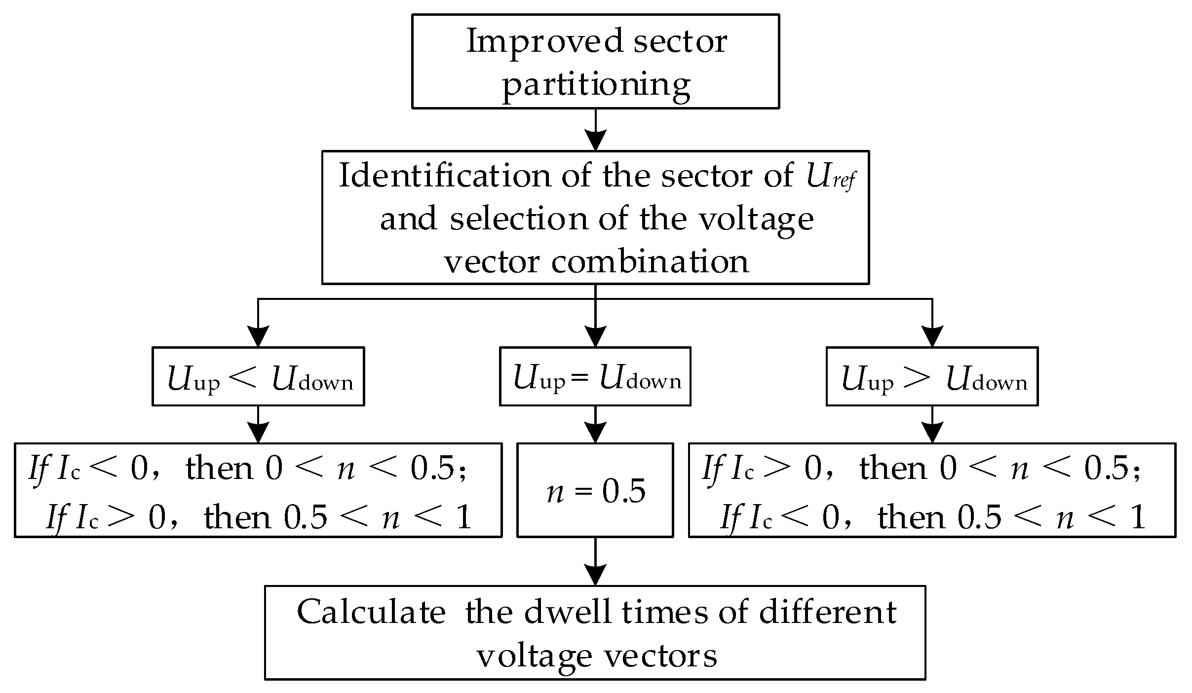
Within one switching period, once the reference voltage vector, Uref, is given, all basic vectors located in the corresponding sector can be selected to synthesize the reference vector. To regulate and compensate for potential neutral-point voltage imbalance on the DC side, a small-vector dwell-time coefficient, n (0 < n < 1), is introduced, by which the dwell times of the small vector and its redundant counterparts are appropriately adjusted.
After introducing the small-vector dwell-time coefficient, n, the resulting expression can be written as
By substituting Equations (4) and (5) into Equation (3), the results summarized in
Table 4 can be obtained. Under the condition of a balanced neutral-point voltage, the small-vector dwell-time coefficient satisfies
n = 0.5. In contrast, under neutral-point voltage imbalance, the value of
n should be adjusted according to the relationships given in
Table 4.
After introducing the actual upper and lower DC-link capacitor voltages, the sector boundaries originally defined under the ideal assumption of symmetrical DC voltages are no longer valid and therefore must be reconfigured accordingly.
Within the conventional SVPWM modulation framework, this paper redefines the sector determination criteria of the reference voltage vector to ensure correct vector selection and synthesis under neutral-point voltage imbalance conditions. On this basis, combined with the modified volt–second balance-based dwell-time calculation, an SVPWM control scheme suitable for neutral-point voltage regulation is established. The overall control structure is illustrated in
Figure 5.
Compared with conventional SVPWM, the proposed strategy improves the consistency between vector selection and dwell-time calculation during neutral-point voltage deviation by introducing dynamic sector boundary reconstruction and volt–second balance correction. As a result, the reference voltage vector can be synthesized more accurately throughout the neutral-point balancing process. This effectively mitigates the AC-side waveform distortion that commonly occurs during neutral-point recovery with traditional methods and leads to improved harmonic performance of the grid-side current.
Compared with conventional SVPWM, the proposed strategy improves reference vector synthesis under neutral-point deviation through two coordinated mechanisms: dynamic sector boundary reconstruction avoids sector misclassification caused by unequal split-capacitor voltages, while dwell-time correction based on the modified volt–second balance eliminates the mismatch between the computed and actual vector contributions. As a result, the synthesized voltage vector more closely tracks the reference vector during the neutral-point balancing process, thereby suppressing AC-side waveform distortion and reducing grid-current harmonic degradation.
5. Boundary Modeling and Power Allocation Control Under Unbalanced Load Conditions
5.1. Boundary Condition Modeling: Average Power Ratio Constraint of Resistive Loads
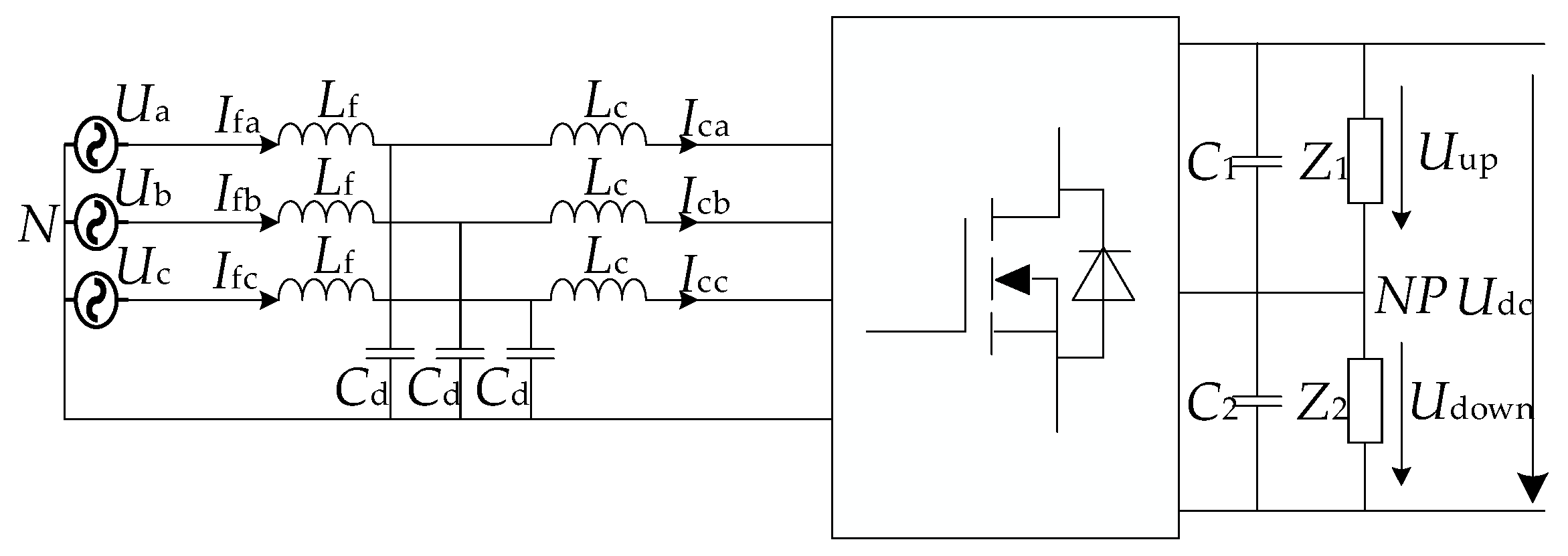
The three-phase 5L-ANPC converter system with DC-side unbalanced loads is illustrated in
Figure 6, where
If denotes the grid-side input current,
Ic represents the converter input current at the DC interface, and
Z1 and
Z2 are the resistive loads connected in parallel with the upper and lower DC-link capacitors
C1 and
C2, respectively.
Figure 7 is introduced for average-power modeling under DC-side unbalanced loads. By partitioning one fundamental cycle into different sector intervals, it enables separate evaluation of the contributions of the involved voltage vectors to the upper and lower branch powers, which forms the basis for the derivation of the proposed load power boundary condition.
According to
Figure 7, the average load powers considered in this paper refer to the time-averaged values of the instantaneous powers absorbed by the upper and lower DC-side loads over one fundamental period, i.e., the net branch energy-transfer rates on the fundamental-cycle timescale. For load
Z1, the average power over one fundamental period, denoted as
Pup, consists of the average-power components contributed by Mode P and Mode HP
+, i.e.,
PP and
PHP+. Similarly, the average power of load
Z2, denoted as
Pdown, is composed of the power components associated with Mode P and Mode HP
−, i.e.,
PP and
PHP+.
The corresponding expressions are given as follows:
In the ideal case, where the conduction loss, switching loss, and other parasitic energy losses of the converter are neglected, the average AC-side power,
Pac, over one fundamental period equals the average DC-side power,
Pdc, satisfying the power balance implied by energy conservation. In this case, the DC-side average power is jointly determined by the average powers absorbed by the loads connected across the upper and lower split DC-link capacitors, i.e.,
For the converter operation in the positive half-cycle shown in
Figure 6, the interval is uniformly divided into
k segments. Specifically, indices 0~
i correspond to the first segment of Sector II (0~
T1), indices
i + 1~
j correspond to Sector I (
T1~
T2), and indices
j + 1~
k correspond to the second segment of Sector II (
T2~
T3). Accordingly, the power expressions of the load
Z1 (connected to the upper capacitor) and the load
Z2 (connected to the lower capacitor) can be explicitly written as follows:
By simplification, the following expression is obtained:
From the above analysis, it can be observed that the power ratio between the upper and lower loads is closely related to the dwell times of different voltage vectors over one fundamental period. Since the dwell-time expressions of the outer voltage vectors, small voltage vectors, and zero voltage vectors vary across modulation sectors, the contribution of each sector must be evaluated separately when formulating the load power relationship. Accordingly, the upper-to-lower load power ratio should be expressed as a weighted superposition of the dwell times of the involved vectors in each sector, while accounting for their distinct effects on the discharge paths of the upper and lower DC-link capacitors. Moreover, under the balanced steady-state condition,
Therefore, the analytical expression of the average-power ratio between the upper and lower loads is given by
where
Equation (12) constitutes the core analytical expression of the proposed load power boundary model. It describes the upper-to-lower average load power ratio as a function of the reference voltage magnitude, Uref, and the small-vector duty factor, n, and thereby characterizes the feasible operating region for neutral-point regulation under DC-side unbalanced-load conditions.
From the derived average-power expression, it follows that the boundary condition is jointly determined by the reference voltage vector, Uref, and the small-vector dwell-time factor, n. Since Uref is a function of the modulation index, m, the admissible range of load power imbalance varies noticeably with different combinations of m and n.
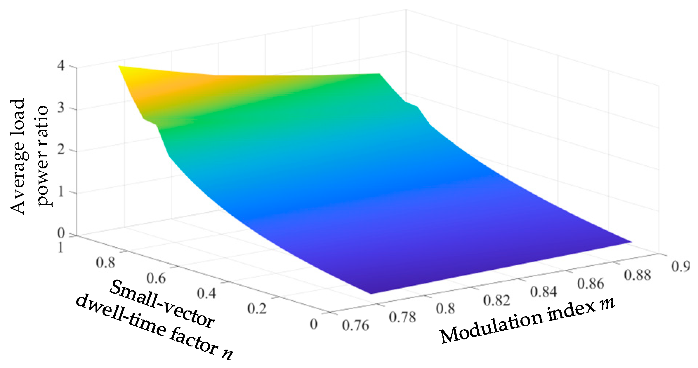
To better illustrate this dependence, the boundary condition is visualized in the three-dimensional plot shown in
Figure 8, which highlights the coupled influence of
m and
n on the load boundary. In this figure, the horizontal axis represents the modulation index,
m, i.e., the ratio of the reference voltage magnitude to the DC-bus voltage; the vertical axis represents the small-vector dwell-time factor,
n, which specifies the time-sharing ratio of the redundant small vectors within one switching period; and the third axis denotes the average load power ratio,
Pup/
Pdown, which quantifies the degree of load power imbalance under different modulation settings.
To better illustrate the proposed boundary model, the relationship described by Equation (12) is visualized in the three-dimensional plot shown in
Figure 8. The surface reveals the coupled influence of the modulation index,
m, and the small-vector duty factor,
n, on the average load power ratio and thus provides a graphical interpretation of the admissible load power imbalance boundary.
As shown in
Figure 8, the average load power ratio,
Pup/
Pdown, exhibits an overall decreasing trend as the modulation index,
m, increases. This is mainly because, under high modulation conditions, the dwell times of the available vectors tend to approach their limiting values, which compresses the adjustable dwell-time margin of the small voltage vectors. Consequently, the neutral-point regulation capability relying on redundant small-vector allocation is weakened. Meanwhile, when the small-vector dwell-time factor,
n, approaches 0 or 1,
Pup/
Pdown becomes much more sensitive to
n and varies more sharply, indicating that an excessive bias toward a single redundant small vector alters the power-sharing behavior between the upper and lower branches and thereby degrades the controllability of the neutral-point balance.
Overall, the three-dimensional surface reveals the coupled influence of m and n on the load boundary: m determines the overall scale of the small-vector regulation margin, whereas n determines the direction and sensitivity of power redistribution within that margin. These results provide a quantitative basis for optimizing the small-vector allocation strategy and for identifying the feasible operating boundary of the system in terms of neutral-point voltage balancing capability.
5.2. Battery-Load Power Allocation and Charging/Discharging Current Regulation
The three-phase 5L-ANPC converter system with DC-side battery loads is illustrated in
Figure 9.
Based on the power-transfer mechanism, the previous section established the average-power constraints under DC-side load imbalance, which delineate the achievable power-regulation range under the available modulation degrees of freedom. When battery-type loads are connected on the DC side, the battery terminals exhibit a pronounced voltage-clamping behavior within the control time scale; the terminal voltage is mainly governed by the open-circuit voltage and the equivalent internal resistance and thus cannot be regulated in the same manner as resistive loads via DC-link capacitor-voltage dynamics.
In this study, the battery-type loads considered in the verification are modeled as Nickel–Metal Hydride (NiMH) batteries, which are used here as representative voltage-source-type loads.
Therefore, the control objective under battery operation is no longer centered on enforcing a strictly balanced neutral-point potential, but is reformulated as achieving controllable power routing and charge/discharge current regulation under permissible voltage asymmetry.
Within this framework, the role of the small-vector duty factor, n, is further extended from neutral-point regulation to branch power-allocation control. Within the feasible operating region derived in the previous section, the subsequent formulation establishes the mapping between n and the average branch power/current ratio, so that the desired power-sharing command can be achieved through constrained online calculation and smoothing of n. In this way, the proposed method converts the modulation degree of freedom into a practically implementable control variable for battery-load power distribution.
Accordingly, the control problem is posed as follows: with the measured upper- and lower-port voltages, Uup and Udown, the redundancy of SVPWM small-vector allocation is exploited by treating the small-vector dwell-time factor, n, as an online control input to command the desired sharing of the average power (or charge/discharge current) between the upper and lower battery branches. If the requested power share exceeds the reachable range, reference clamping and rate limiting are applied to preserve the continuity of the allocation process and ensure stable operation. To mitigate parameter jitter and improve implementability, voltage-measurement filtering and a constraint on the variation rate of n are introduced, and an implementation procedure compatible with the existing current closed-loop structure is provided.
To enable controllable power routing for the battery-type DC ports, this study directly regulates the power-sharing ratio of the average power between the upper and lower ports. The reference command for the upper-port power share is defined as
To maintain consistency with the previously derived average-power-ratio boundary, the desired power ratio,
ρ*, is introduced as
Therefore, enforcing the actual power ratio,
ρ, to track the reference,
ρ,
* is equivalent to making the power-sharing factor,
λ, follow its command,
λ*. Substituting Equation (11) into the above relationship yields
Based on the derived boundary model, the subsequent equations do not merely restate classical relationships but extend the analysis toward controllable battery-load power-sharing by explicitly linking the small-vector duty factor to branch power/current allocation.
Based on the above expressions, the adjustable power-sharing control can be reformulated as an online solution for
n. Due to the limited modulation redundancy, to avoid infeasible solutions or numerical divergence,
n is constrained within
n∈[
nmin,
nmax] in implementation (typically
nmin = 0.01 and
nmax = 0.99 to prevent singularities), and the achievable range of the power-ratio distribution is then calculated as
When the externally specified
ρ* lies outside the achievable domain, the equation
f(
n) =
ρ* has no exact solution. To ensure control feasibility, a reference-clamping strategy is adopted:
and
ρ*
used is taken as the actual target for the online solver, thereby achieving a power allocation that is closest to the desired reference while remaining within the feasible region.
Although, under ideal conditions, the total DC-side power in a three-phase system does not exhibit the characteristic double-frequency ripple typically observed in single-phase operation, the measured port voltages still contain switching ripple and sampling noise. To mitigate the influence of measurement disturbances on the online solution, a lightweight first-order discrete low-pass filter is applied to the port-voltage measurements:
In Equation (18),
where
Ts denotes the update period of
n and
τv is selected on the order of milliseconds to balance ripple attenuation and dynamic response. In the online solver,
f(
n) uses the filtered voltages
Uup,f and
Udown,f as inputs instead of the instantaneous measurements.
Moreover, to ensure the continuity of the SVPWM modulation and to prevent waveform distortion caused by abrupt changes in
n between adjacent update intervals, a rate-limiting constraint is introduced:
where ∆
nmax can be selected according to the control period and the required system dynamics.
By summarizing the above procedure, the following error function is defined:
The equation g(n) = 0 is solved online using a coarse bracketing search combined with the bisection method as follows:
Within [
nmin,
nmax], a scanning step, ∆
n, is applied to identify a sign-change interval, [
nL,
nR], such that
- 2.
Bisection iteration:
If a valid bracketing interval is found, the bisection method is performed over [nL,nR] until the prescribed tolerance is satisfied or the maximum number of iterations is reached, yielding nraw.
- 3.
No-root handling:
If no sign-change interval exists, the value of n that minimizes over [nmin,nmax] is selected as nraw, thereby achieving the closest attainable power allocation within the feasible domain.
Finally, nraw is subjected to rate limiting and saturation to generate n(k), which is fed into the SVPWM module to allocate the dwell times of redundant small vectors in real time. The proposed solver relies only on algebraic evaluations and a bounded number of iterations, resulting in low computational cost and straightforward implementation in Simulink or real-time platforms. It can run in parallel with the conventional outer PI/inner PR current control loops: the inner loop maintains grid-current quality, whereas the power-sharing function adjusts DC-side energy routing via n.
In summary, a DC-side adjustable power-sharing scheme for battery-type loads is developed. Using the supervisory reference, λ*, n is obtained online with feasible-domain clamping, voltage-measurement filtering, and rate constraints to ensure stable operation. The framework is extensible to multi-port coordination and can incorporate SoC constraints, current limits, and efficiency-oriented optimization for multi-objective energy management.
6. Experimental Results
To validate the correctness of the theoretical analysis and its practical feasibility, hardware-in-the-loop (HIL) experiments were conducted on the OP5707 real-time simulation platform (OPAL-RT Technologies). According to the verification objective, both single-phase and three-phase 5L-ANPC systems were implemented. The single-phase system is mainly used to verify the derived average-power boundary condition for resistive loads by examining the convergence or divergence of the split-capacitor voltages under different upper/lower load power ratios. The three-phase system is employed to validate the proposed adaptive modulation strategy and the battery-load power-sharing control, since the battery-load case is more suitably assessed in a three-phase configuration to avoid the second-order power ripple inherent to single-phase operation.
The OP5707 integrates multi-core real-time processors and FPGA computing resources, enabling hard real-time numerical solution of power-electronic systems and thereby facilitating rapid modeling and controller validation for multilevel converters under various operating conditions. In this study, the Simulink models of the single-phase and three-phase 5L-ANPC converters were deployed to the OP5707 real-time target via RT-LAB. Key electrical variables, including voltages and currents, were acquired and interfaced through an adapter board and analog I/O modules. The control and modulation signals were generated online by the OP5707 under hard real-time constraints and directly applied to the gate-triggering logic of the power switches, ensuring real-time execution of the proposed control strategy.
For waveform observation, the relevant output signals of an OP5707-based hardware-in-the-loop (HIL) platform sourced from OPAL-RT Technologies (Montreal, QC, Canada) were fed into an oscilloscope, while the harmonic spectrum and THD results reported later were obtained separately using a PQ3198 power quality analyzer sourced from HIOKI E.E. Corporation (Ueda, Nagano, Japan).
Under identical controller parameters, sampling/PWM update settings, and initial operating conditions, the HIL tests were then carried out to compare the conventional and proposed modulation strategies, to verify the derived average-power boundary condition for resistive loads, and to validate the battery-load power-sharing performance in the three-phase system.
The representative main-circuit parameters of the 5L-ANPC converter are summarized in
Table 5. Since the three-phase converter adopts identical main-circuit parameters in each phase, one phase is taken as an example for parameter listing.
Accordingly, the rated power P = 10kW denotes the rated power of one single-phase power unit.
To further eliminate the influence of the control loops, the following conditions were kept identical in the experiments: (1) the controller parameters of the outer voltage loop and the inner current loop; (2) the sampling, filtering, and PWM update periods; and (3) the load configuration and the initial capacitor voltages.
In the three-phase system, Uac = 220 V is the phase RMS voltage, corresponding to a line-to-line RMS voltage of approximately 380 V, whereas Udc = 400 V is the total DC-link voltage.
It should be noted that some annotations appearing in the figures are displayed in Chinese due to the default settings of the measurement instruments. These Chinese labels correspond to standard engineering terms and units. For example, “次/秒” denotes “cycles per second,” which is equivalent to hertz (Hz). All such annotations have been interpreted accordingly in the manuscript.
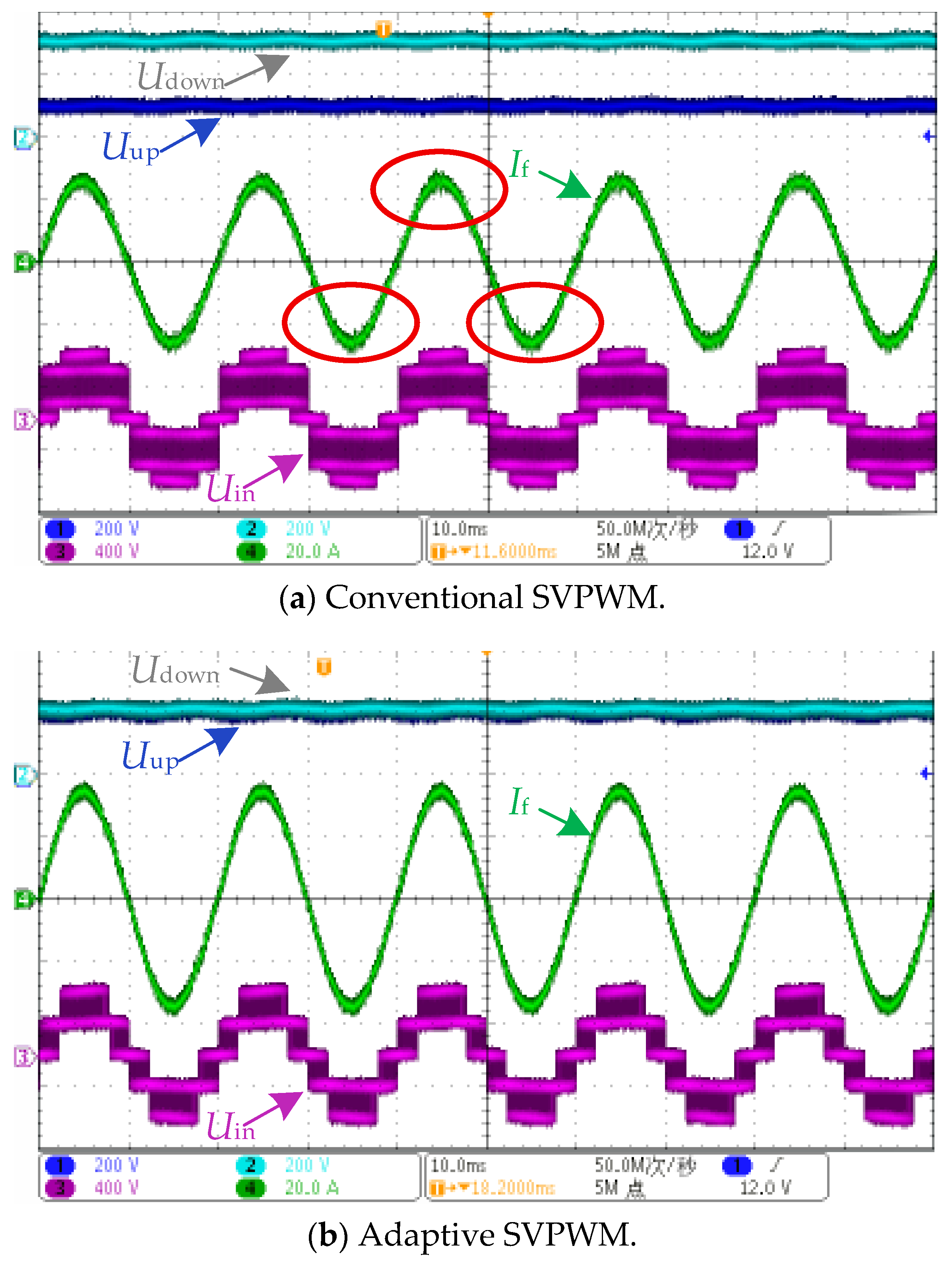
Figure 10a,b compare the experimental waveforms obtained with conventional SVPWM and the proposed adaptive SVPWM accounting for neutral-point offset, respectively. As shown in
Figure 8, the conventional sector partitioning weakens neutral-point balancing and degrades the AC-side current waveform quality. This is mainly because conventional SVPWM is derived under the assumption of symmetric DC-link capacitor voltages; when neutral-point deviation changes small-vector magnitudes, insufficient sector identification and volt–second balance updating can cause the synthesized voltage vector to deviate from the reference, thereby deteriorating the current waveform.
The Chinese label “50M次/秒” in the oscilloscope screenshot denotes a sampling rate of 50 MS/s (50 mega-samples per second).
Figure 10a shows the experimental waveforms under conventional SVPWM. With DC-link capacitor-voltage imbalance, the modulation is still derived under the symmetry assumption; thus, the sector identification and volt–second balance are not updated with the neutral-point deviation, resulting in neutral-point imbalance and degraded AC-side current waveform quality.
Figure 10b shows the experimental waveforms under the adaptive SVPWM considering neutral-point voltage offset. The scheme re-partitions the sectors and corrects the volt–second balance using the measured capacitor voltages, such that the selected vectors and dwell times are updated online with the neutral-point deviation. Consequently, the neutral-point voltage remains stable during transients, and the AC-side current exhibits improved sinusoidality with reduced distortion.
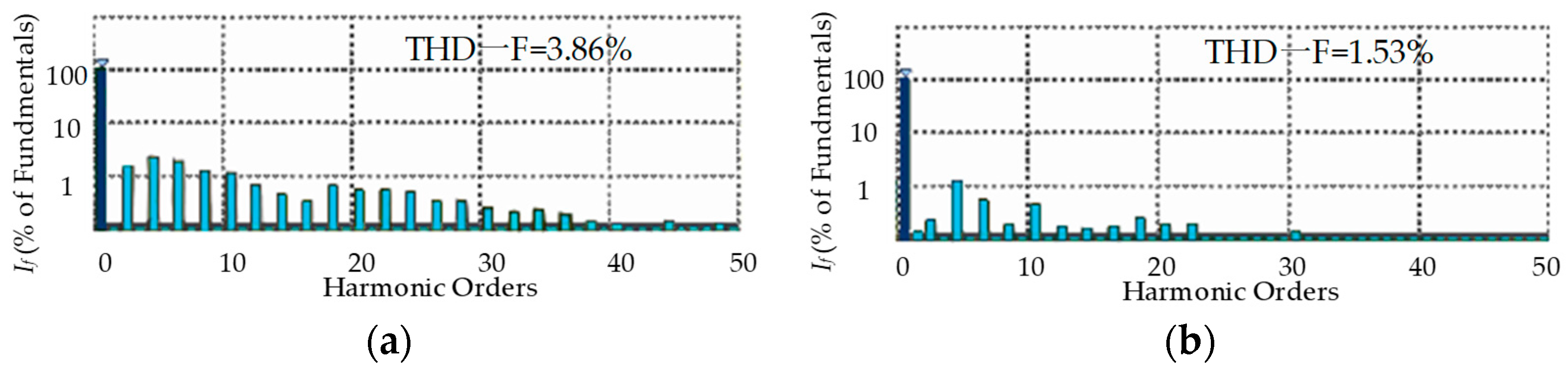
The grid-side input current is measured using a HIOKI PQ3198 for harmonic analysis and THD evaluation (referenced to the 50 Hz fundamental, with the instrument’s default window and calculation settings). During regulation with conventional SVPWM, the measured current, THD, is approximately 3.86%, as shown in
Figure 11a. By comparison, with the adaptive SVPWM considering neutral-point voltage offset, the neutral-point voltage fluctuation is reduced to some extent, which helps alleviate waveform degradation associated with sector misidentification and volt–second mismatch in the conventional approach; consequently, the current, THD, decreases to about 1.53%, as shown in
Figure 11b.
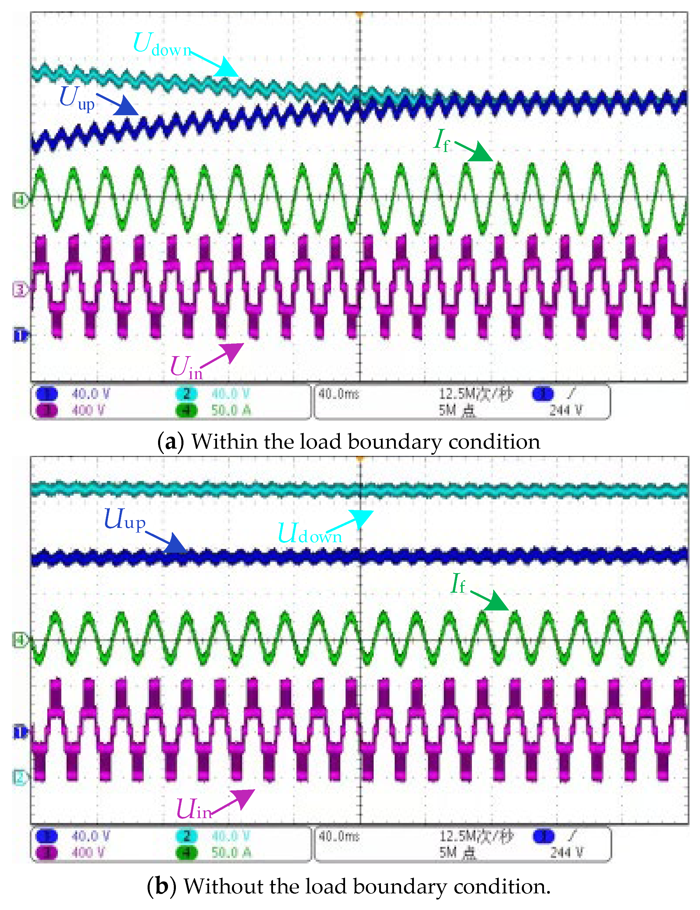
For resistive-load boundary verification, a total of six test cases were carried out, with the upper-to-lower average load power ratio varying from 0.25 to 4. For each case, the capacitor-voltage evolution was observed over 1 s to evaluate whether neutral-point regulation could be maintained. The results show that the capacitor voltages converge when the load power ratio lies within the derived boundary and diverge once the boundary is exceeded. In addition, the closer the operating point is to the derived boundary, the slower the balancing process becomes.
When the upper-to-lower load power ratio satisfies the derived boundary condition, the experimental waveforms in
Figure 12a show that the upper and lower capacitor voltages gradually converge, accompanied by a noticeable reduction in neutral-point voltage fluctuation. In contrast, when the load power ratio exceeds this boundary,
Figure 12b indicates that the capacitor voltages tend to diverge, and the neutral-point deviation increases, exhibiting a more pronounced imbalance.
The Chinese label “12.5M次/秒” in the oscilloscope screenshot denotes a sampling rate of 12.5 MS/s (12.5 mega-samples per second).
As shown in
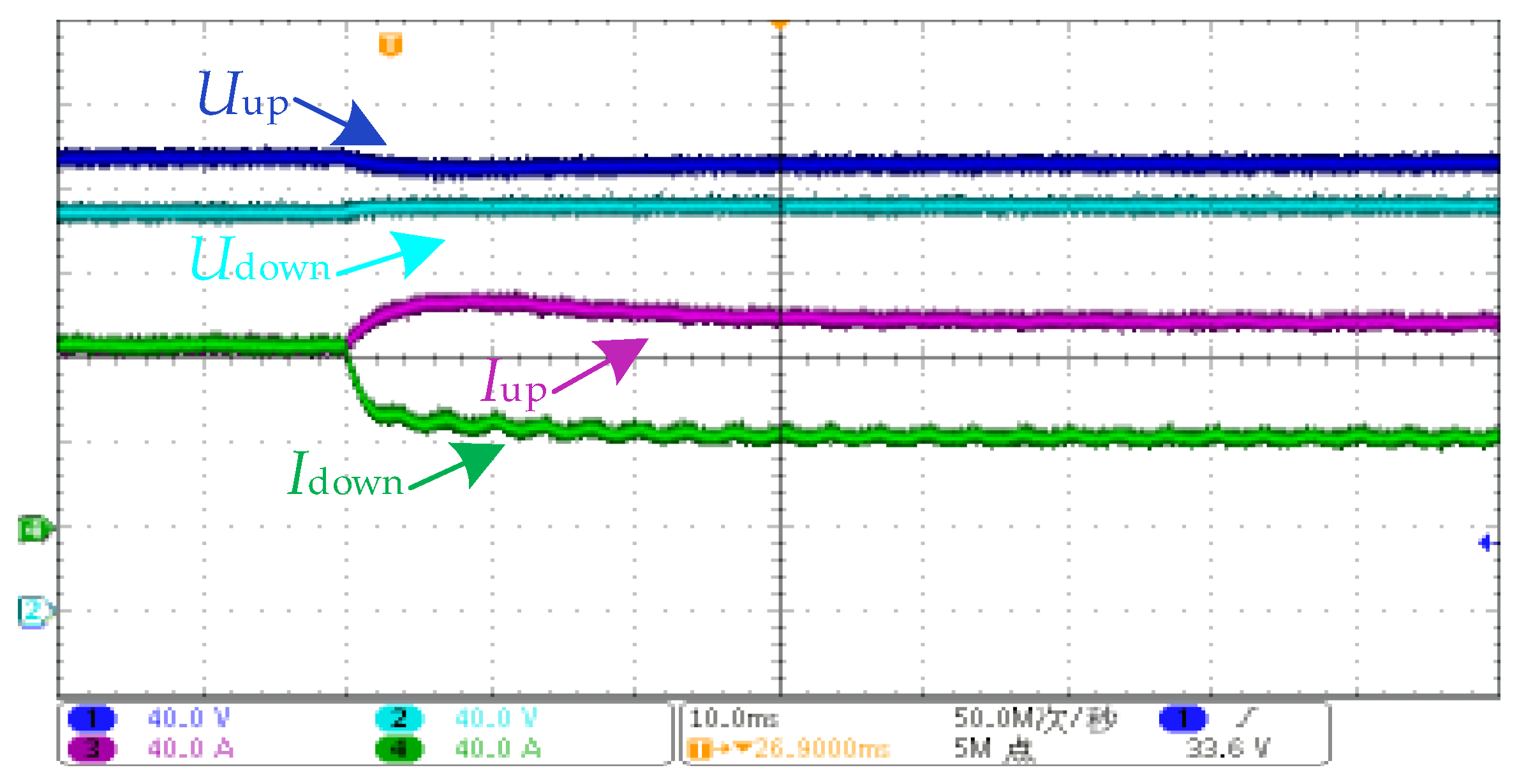
Figure 13, when the battery-type load power ratio is switched from 1:1 to 3:1, the DC-side currents are redistributed accordingly: the upper-port current decreases while the lower-port current increases to track the updated power-sharing reference, where
Iup and
Idown denote the currents flowing through the upper and lower battery-type loads, respectively.
The Chinese label “50M次/秒” in the oscilloscope screenshot denotes a sampling rate of 50 MS/s (50 mega-samples per second).
During the transient process, the upper and lower capacitor voltages exhibit limited deviation and gradually converge to new steady-state values. No divergence or sustained oscillation can be observed, indicating that the operating point remains within the derived feasible boundary.
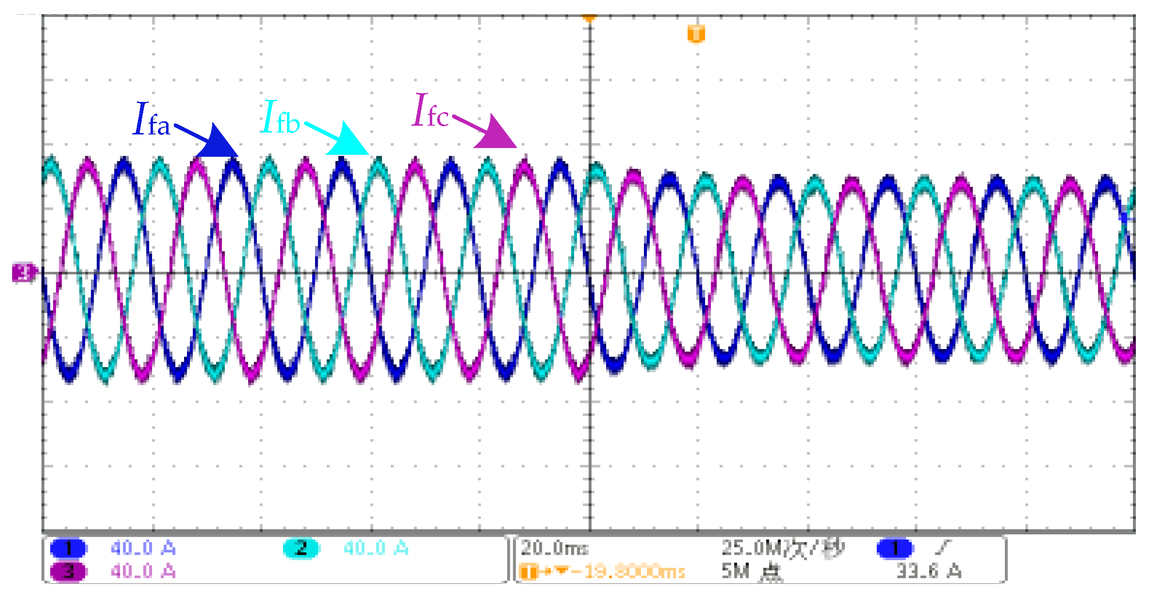
As shown in
Figure 14, the three-phase grid-side currents maintain satisfactory sinusoidal characteristics during the power transition. No noticeable waveform distortion or low-frequency envelope oscillation can be observed, indicating that the power redistribution implemented via the small-vector allocation coefficient does not introduce significant interference to the inner current control loop.
The Chinese label “25M次/秒” in the oscilloscope screenshot denotes a sampling rate of 25 MS/s (25 mega-samples per second).
7. Conclusions
This paper investigates rectifier-mode operation with a three-terminal DC bus and unbalanced loads. An adaptive SVPWM scheme is proposed by re-partitioning sectors and correcting the volt–second balance using measured DC-link capacitor voltages, which improves reference vector synthesis under neutral-point deviation and alleviates AC-side current waveform degradation.
A boundary condition on the average load power is further derived to characterize the admissible load power ratio for maintaining neutral-point balance without additional hardware. Experiments with resistive loads confirm convergence of the capacitor voltages within the derived boundary and divergence once it is exceeded.
The method is also extended to battery-type loads by introducing a DC-side power-sharing control that adjusts the small-vector dwell-time coefficient online to realize dynamic power redistribution between battery ports, while maintaining satisfactory grid-current quality during power-sharing transitions.
Hardware-in-the-loop tests on an OP5707 platform validate the real-time feasibility and dynamic performance of the proposed approach.
Future work will involve a low-power hardware prototype to further evaluate the proposed method under practical non-ideal conditions. The planned tests will include steady-state waveform measurements, dynamic load/power-sharing transition tests, switching-behavior observation under dead time and parasitic effects, and thermal-stress assessment so as to examine how these non-ideal factors influence neutral-point regulation, reference vector synthesis accuracy, power-sharing performance, and current waveform quality.