Article

A VSG Transient Improvement Method from the Perspective of Equivalent Circuits


1
Huizhou Power Supply Bureau, China Southern Power Grid Co., Ltd., Huizhou 516000, China
2
Electric Power Research Institute, China Southern Power Grid Co., Ltd., Guangzhou 510080, China
*
Author to whom correspondence should be addressed.
Energies 2026, 19(6), 1575; https://doi.org/10.3390/en19061575
Submission received: 24 October 2025 / Revised: 14 November 2025 / Accepted: 26 November 2025 / Published: 23 March 2026
(This article belongs to the Special Issue Energy, Electrical and Power Engineering: 5th Edition)

Abstract

Virtual Synchronous Generator (VSG) has become a prominent candidate to control grid-tied power electronic inverters for its ability to provide inertial support and improve power system frequency stability. However, under disturbances, VSG exhibits significant oscillations in its output frequency and power. Meanwhile, existing oscillation suppression methods rely on somewhat complex modeling and cumbersome parameter tuning. To address this issue, this paper proposes a straightforward approach to improving the transient performance of VSG based on the equivalent circuit model of the VSG active power loop. First, it is shown that the parameters in the VSG active power loop have a one-to-one correspondence with the elements of a RLC circuit. Based on the equivalent circuit model of VSG control, it is demonstrated that under the constraints of ROCOF and power–frequency droop limitation, oscillation suppression cannot be effectively achieved only by parameter tuning. Thus, an additional damping resistance branch is introduced into the VSG equivalent circuit model. The quantitative parameter design method of this damping branch is further introduced. Finally, high-power experiments demonstrate that the proposed method effectively suppresses power oscillations and enhances the transient performance of VSGs.

1. Introduction

In recent years, the penetration rate of the renewable energy sources in power systems has been increasing rapidly [1,2,3]. Unlike the traditional power systems with synchronous generator-based voltage sources, power electronics-based grid-connected converters would become the key interfaces to the power grid dominated by renewable energy sources [4,5,6].
Based on the inverter operating characteristics in power systems, grid-connected inverters can be categorized into grid-forming (GFM) inverters and grid-following (GFL) inverters [7,8,9,10]. GFM inverters can output a stable voltage through closed-loop voltage control and can be approximately equivalent to an ideal AC voltage source. In contrast, GFL inverters aim to maximize power delivery to the grid by controlling output current and can be equivalent to an ideal AC current source [11,12,13]. Additionally, GFL inverters need to rely on a phase-locked loop (PLL) to obtain grid frequency and phase, while GFM inverters have no such requirement. Moreover, GFM inverters possess the core capability to actively establish and support the grid voltage and frequency references. This characteristic makes GFM inverters highly suitable for application in modern power systems with large-scale renewable energy generation [14,15,16]. VSG control is the most commonly used GFM method. It can provide inertial support and damping support for the power grid. However, while the virtual inertia in VSG contributes to grid frequency stability, it also induces significant oscillations in VSG output frequency and active power under disturbances, which severely impairs the stable operation of VSG.
As the transient behavior of VSG is primarily governed by its virtual inertia and droop coefficient, many studies have attempted to enhance the VSG dynamic response through parameter adaptation. References [17,18,19,20,21] improve the transient performance by dynamically tuning the virtual inertia. Building upon this idea, Reference [22] achieves an approximately critically damped transient response by simultaneously adjusting both the virtual inertia and droop coefficient. Furthermore, Reference [23] establishes a unified parameter adaptation trajectory, which coordinates the variation in both virtual inertia and droop coefficient according to the instantaneous frequency and the rate of change of frequency (ROCOF). However, such adaptive tuning approaches inevitably compromise the inherent inertial support capability of the VSG. To address this limitation, Reference [24] proposes an adaptive droop adjustment strategy, in which only the droop coefficient is updated as an exponential function of ROCOF, thereby maintaining the inertial support while improving transient stability. Although adaptive controls exhibit advantages in handling parameter uncertainties and dynamic variations in practical systems, existing studies have shown that adaptive virtual inertia in VSG control may alter the inherent inertia support characteristics of VSGs, thereby affecting their fundamental dynamic response performance [25,26,27,28].
Power oscillation suppression can also be achieved by modifying the structure of the VSG control loop. Reference [25] proposes a method that incorporates a grid frequency-dependent variable into the damping control loop, which facilitates faster convergence of the VSG frequency toward the grid frequency and thereby mitigates power oscillations. Reference [26] develops a dual-feedback control scheme, in which frequency feedback is incorporated to realize acceleration control, while power feedback provides disturbance compensation. Furthermore, Reference [27] refines both the forward-path transfer function and the feedback coefficients within the VSG control loop, allowing improved damping of power oscillations without compromising the inherent inertial support capability.
Although existing methods can effectively suppress power oscillation, they suffer from issues such as somewhat complex modeling, cumbersome parameter tuning and potential impacts on frequency response characteristics. To address these problems, this paper proposes a straightforward damping method from the perspective of the equivalent circuit model of the VSG active power control loop. Specifically, an additional damping resistance branch is introduced into the VSG equivalent circuit model, thereby providing an intuitive damping path to improve transient performance. The influence of this damping branch on the dynamic response is further analyzed, and a corresponding quantitative design method is proposed. The derivation process and parameter design of this method are more straightforward compared to the existing methods.
The remainder of this paper is organized as follows. Section 2 establishes the small-signal model of the VSG; then, it is shown that the parameters in the VSG active power loop have a one-to-one correspondence with the components within a RLC circuit. Section 3 conducts an in-depth VSG power oscillation study based on equivalent RLC circuit resonances, with the R, L and C being adjusted. The constraint conditions that the equivalent circuit parameters must satisfy are then clarified. Equivalently, oscillation suppression cannot be effectively achieved only by parameter tuning under the constraints of ROCOF and power–frequency droop limitation. Thus, an additional damping resistance branch is introduced into the VSG equivalent circuit model in Section 4, and the quantitative parameter design method of this damping branch is further introduced. Section 5 verifies the effectiveness of the proposed method in suppressing power oscillations through high-power experiments.

2. The VSG Control and Its Equivalent Circuit Model

2.1. Establishment of the VSG Small-Signal Model

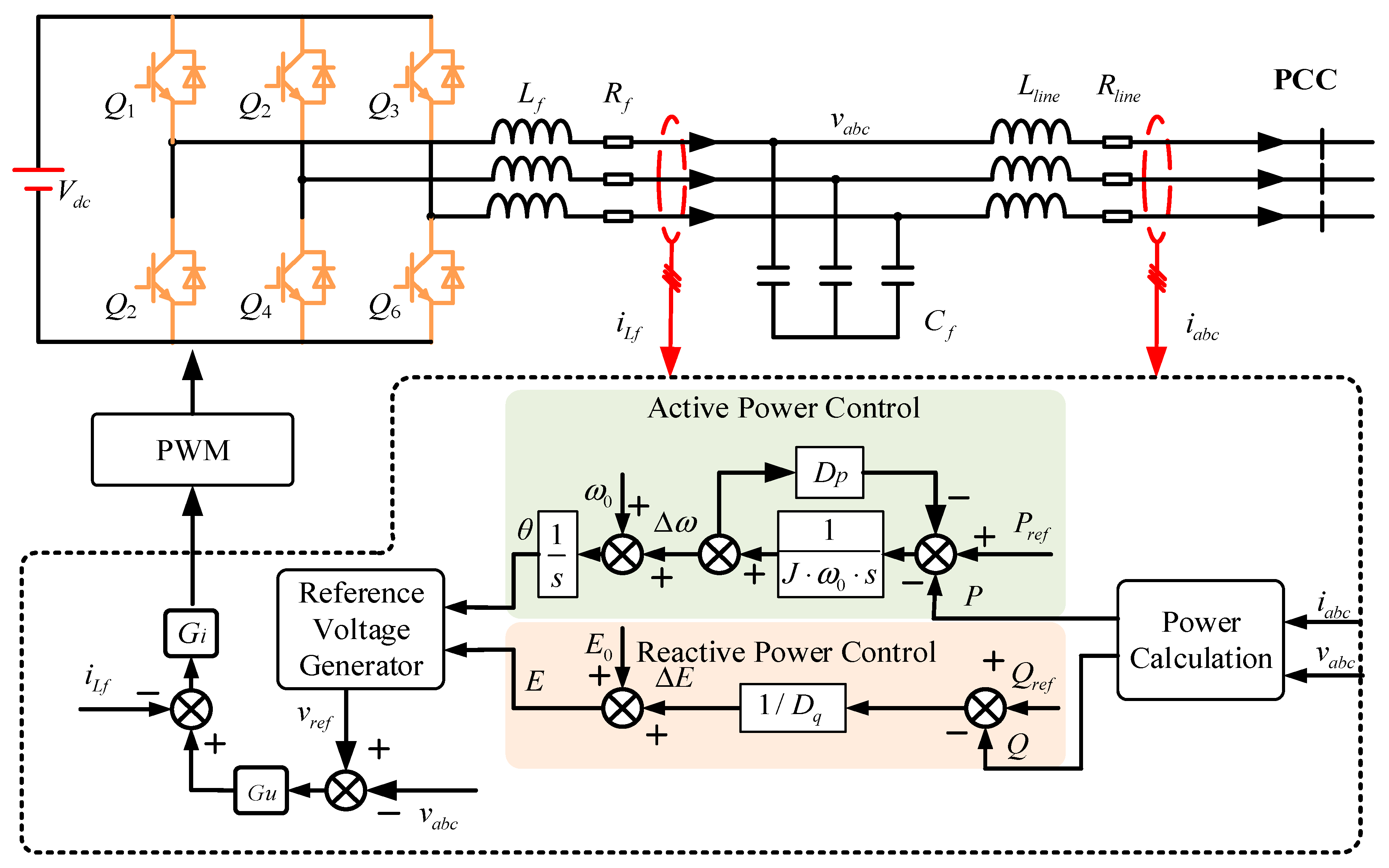
Figure 1 shows the basic structure of the VSG control. Herein, the PWM voltage of the inverter bridge is filtered by an LC filter to obtain the output voltage. Lf and Rf represent the filter inductor and its equivalent series resistance, respectively; Cf denotes the filter capacitor; Lline and Rline stand for the line inductor and line resistance from the output voltage to the Point of Common Coupling (PCC).
By simulating the rotor motion equation of the synchronous generator, the active power control equation of the VSG can be expressed as
P r e f P D p ( ω ω 0 ) = J ω 0 d ω d t ,
where Dp denotes the droop coefficient of VSG; J denotes the virtual inertia of VSG; Pref represents the reference output active power command of VSG; P denotes output active power of VSG; ω denotes the angular velocity; and ω0 denotes the rated angular velocity.
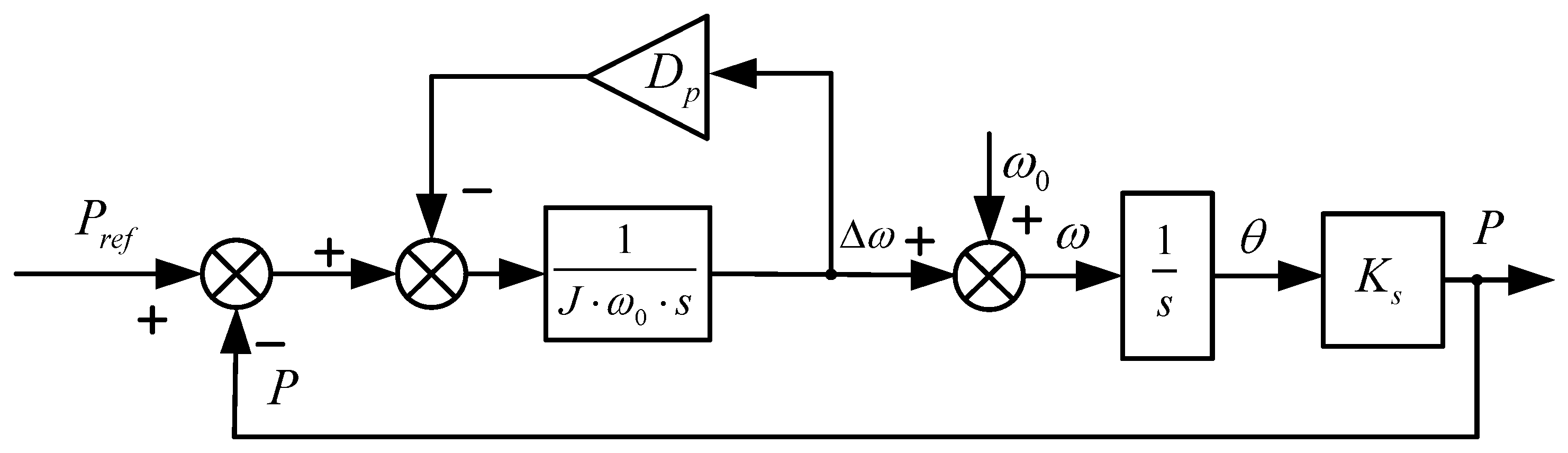
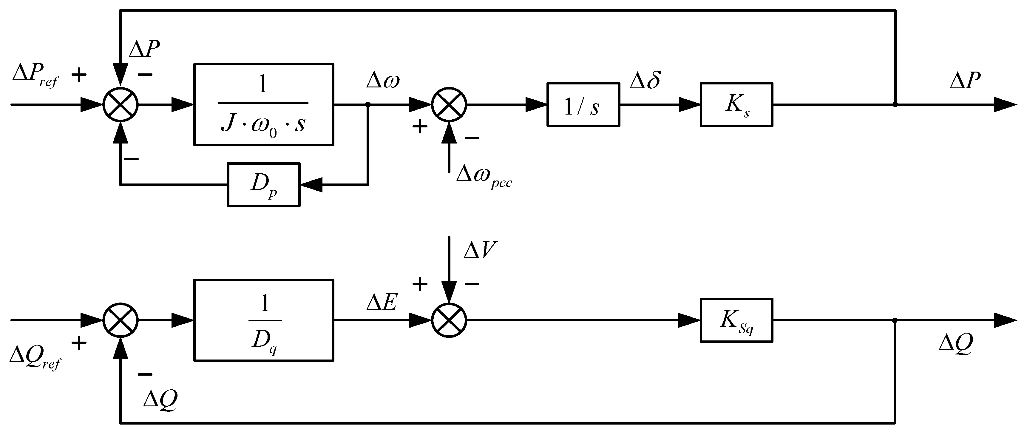
According to Equation (1), the corresponding active power control loop block diagram is shown in Figure 2.
According to the reactive power droop characteristics, the reactive power control equation of VSG can be expressed as
Q r e f Q = D q ( E E 0 ) ,
where Qref denotes the reference reactive power command of VSG; Q denotes the output reactive power of VSG; E denotes the amplitude of the output voltage; E0 denotes the rated amplitude of the output voltage; and Dq is the reactive power droop coefficient.
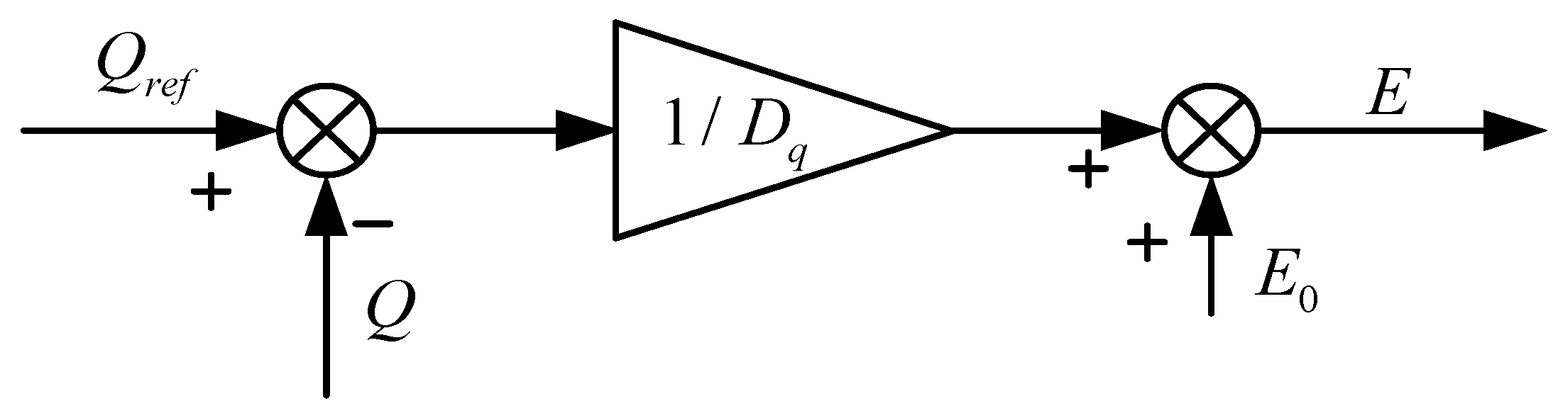
According to Equation (2), the corresponding reactive power control block diagram is shown in Figure 3.
From Equation (1), the small-signal model of the VSG active power controller can be derived as
Δ P r e f Δ P D p Δ ω = J ω 0 s Δ ω
Based on the relationship between the VSG output voltage and the PCC power angle, the following expression can be derived as
Δ δ = Δ ω Δ ω p c c s
By performing small-signal linearization on Equation (2), the small-signal model of the VSG reactive power control can be obtained as
Δ Q r e f Δ Q = D q Δ E
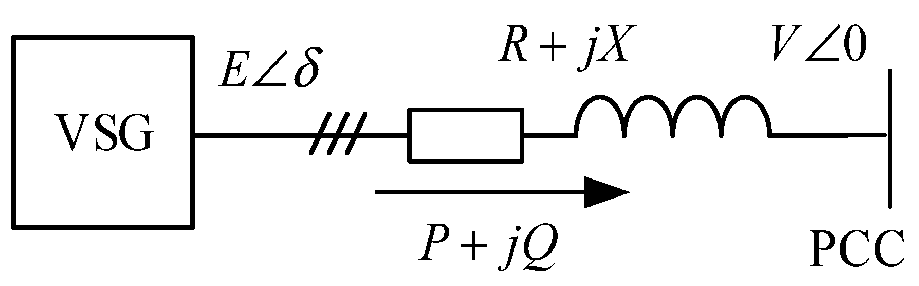
According to Figure 1, its simplified power transmission diagram is illustrated in Figure 4.
In Figure 4, E denotes the output voltage of the VSG, and V denotes the voltage at the PCC. When the circuit satisfies the condition X >> R, the coupling between the active power and reactive power of the VSG can be neglected, and thus the power transmission expression of the VSG can be simplified as
Δ P = 3 2 E V X Δ δ Δ Q = 3 2 V X ( Δ E Δ V )
Combining Equations (3)–(6), the small-signal model block diagram of the VSG can be obtained as Figure 5.
In Figure 5, Ks and Ksq denote the active power and reactive power transmission coefficients, respectively, and can be expressed as
K s = 3 2 E V X K s q = 3 2 V X
It can be seen from Figure 5 that the VSG active power control model can be divided into three components: the power transmission coefficient Ks, the droop coefficient D, and the virtual inertia J, which can be expressed as
( Δ ω Δ ω p c c ) = 1 K s d Δ P d t Δ ω = 1 D p Δ P D Δ P r e f Δ P Δ P D = J ω 0 d Δ ω d t

2.2. Establishment of the Equivalent Circuit Model of the VSG Active Power Loop

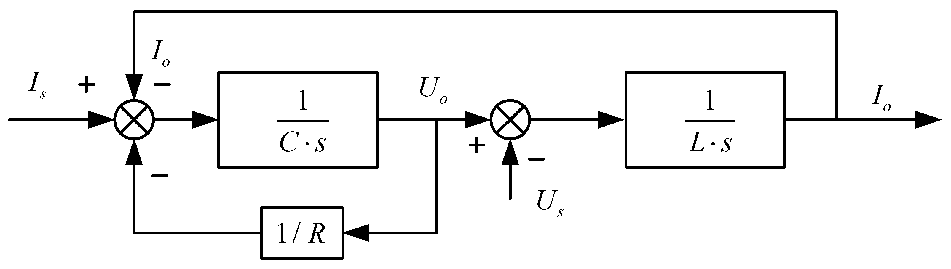
The expressions of the three components in Equation (8) are similar to the linear system models of inductors, resistors, and capacitors in an RLC circuit. Therefore, the three control components of the VSG can be represented by an equivalent RLC circuit, as shown in Figure 6, where the resistor corresponds to the droop coefficient, the inductor corresponds to the power transmission coefficient, and the capacitor corresponds to the virtual inertia. Also, the power command change ∆Pref is represented as an equivalent current source Iref, and the grid frequency disturbance is represented as an equivalent voltage source in the equivalent circuit model.
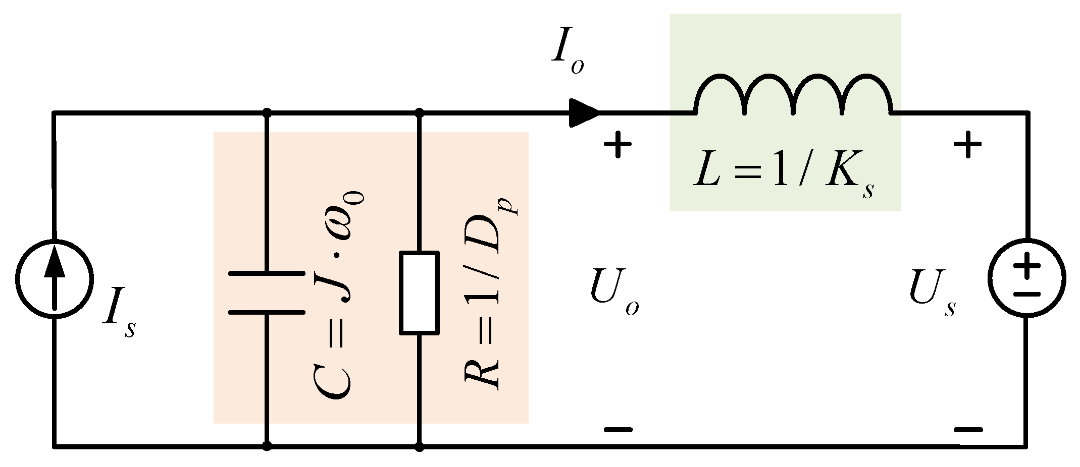
The RLC circuit schematics corresponding to the above dynamic model in Figure 6 is shown as:
The circuit in Figure 7 becomes the equivalent circuit model of the VSG active power loop. The corresponding relationships between the VSG model and the RLC circuit model are summarized in Table 1.
By analyzing the VSG equivalent circuit model in Figure 7, the output current expression can be obtained as
I o = R C L R s 2 + L s + R I s C R s + 1 C L R s 2 + L s + R U s
The output voltage expression of the VSG equivalent circuit model can also be obtained as
U o = L R s C L R s 2 + L s + R I s R C L R s 2 + L s + R U s
Thus, the VSG control power oscillations can be analyzed equivalently as the resonances within an equivalent RLC circuit, as R, L and C parameters vary.

3. VSG Equivalent Circuit Resonance Analysis with Its Constraints

3.1. Parameter Influence on Equivalent Circuit Resonance

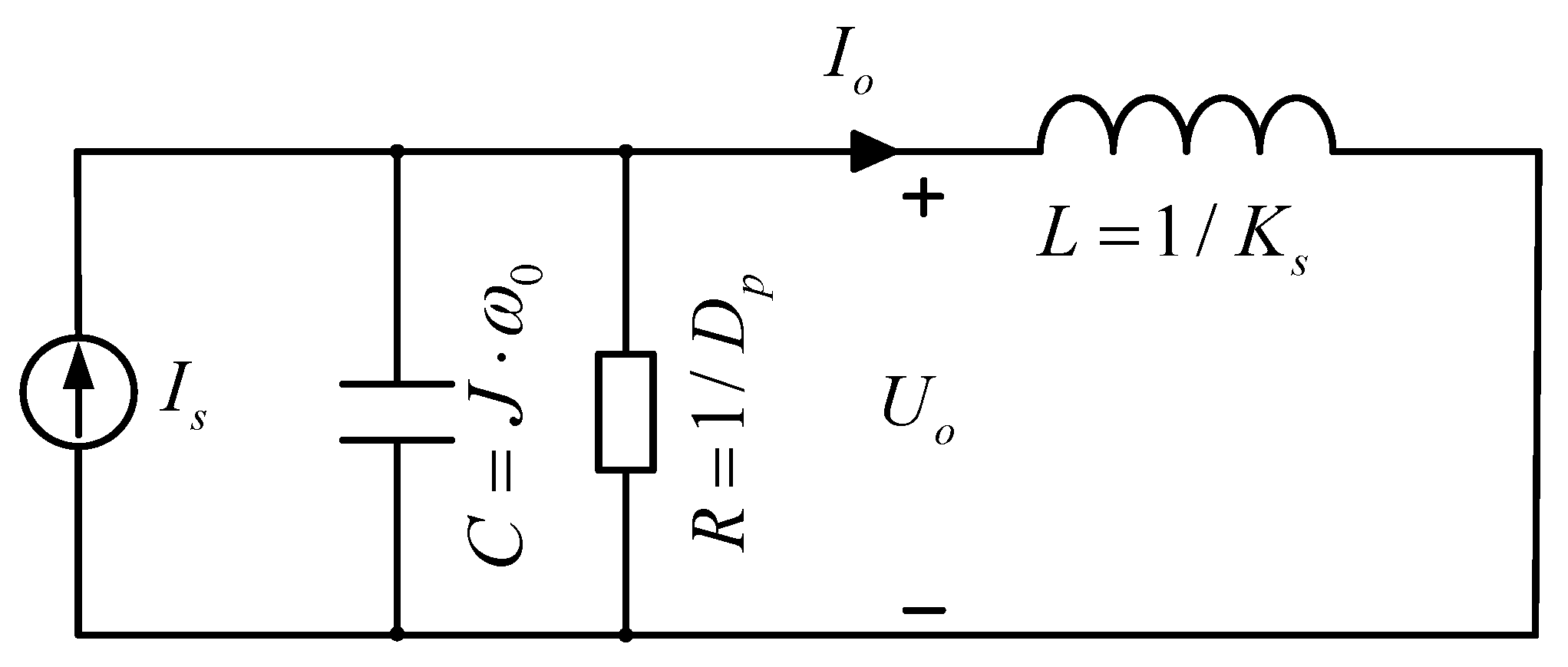
When the VSG operates in grid-connected mode, the usually investigated transient oscillations in output frequency and active power are induced by VSG power command change, while the grid frequency remains stable. Therefore, the equivalent voltage source in Figure 7 is replaced by a short wire as in Figure 8.
Thereby, Equations (9) and (10) can be simplified as
I o = R C L R s 2 + L s + R I s
U o = L R s C L R s 2 + L s + R I s
In the VSG equivalent circuit model, at the instant when Is changes, the capacitor can be regarded as a short circuit; thus, the voltage across its terminals remains zero, meaning that its output voltage remains constant. However, the current flowing through the capacitor at this moment is given by
Δ i C ( 0 ) = I s
Therefore, the rate of change in the capacitor voltage is given by
d U o d t | t = 0 = 1 C Δ i C ( 0 )
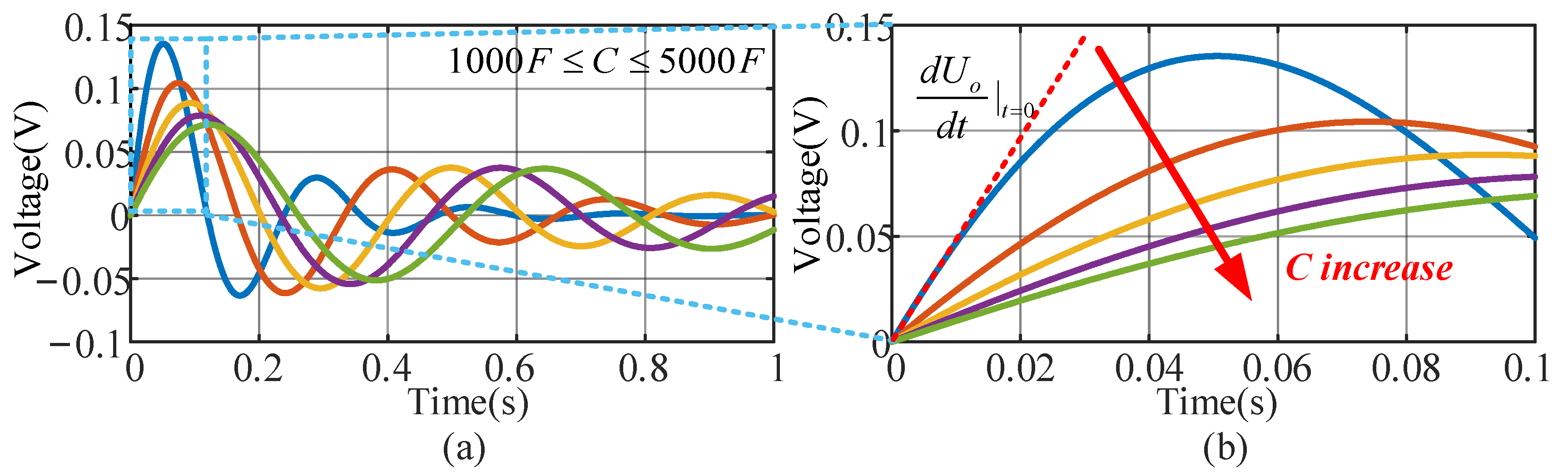
Therefore, by varying the capacitance, the output voltage waveforms can be obtained as shown in Figure 9.
It can be observed from Figure 9 that as the capacitance increases, the initial output voltage change rate gradually decreases, which indicates that the capacitor can stabilize the output voltage of the VSG equivalent circuit model.
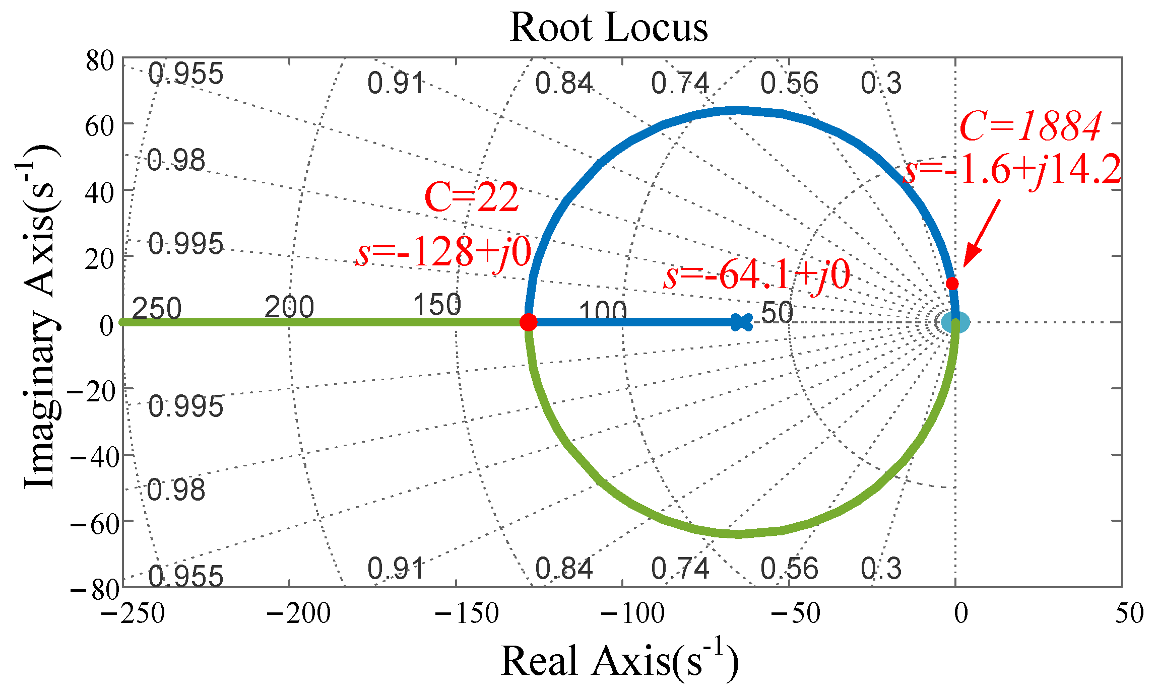
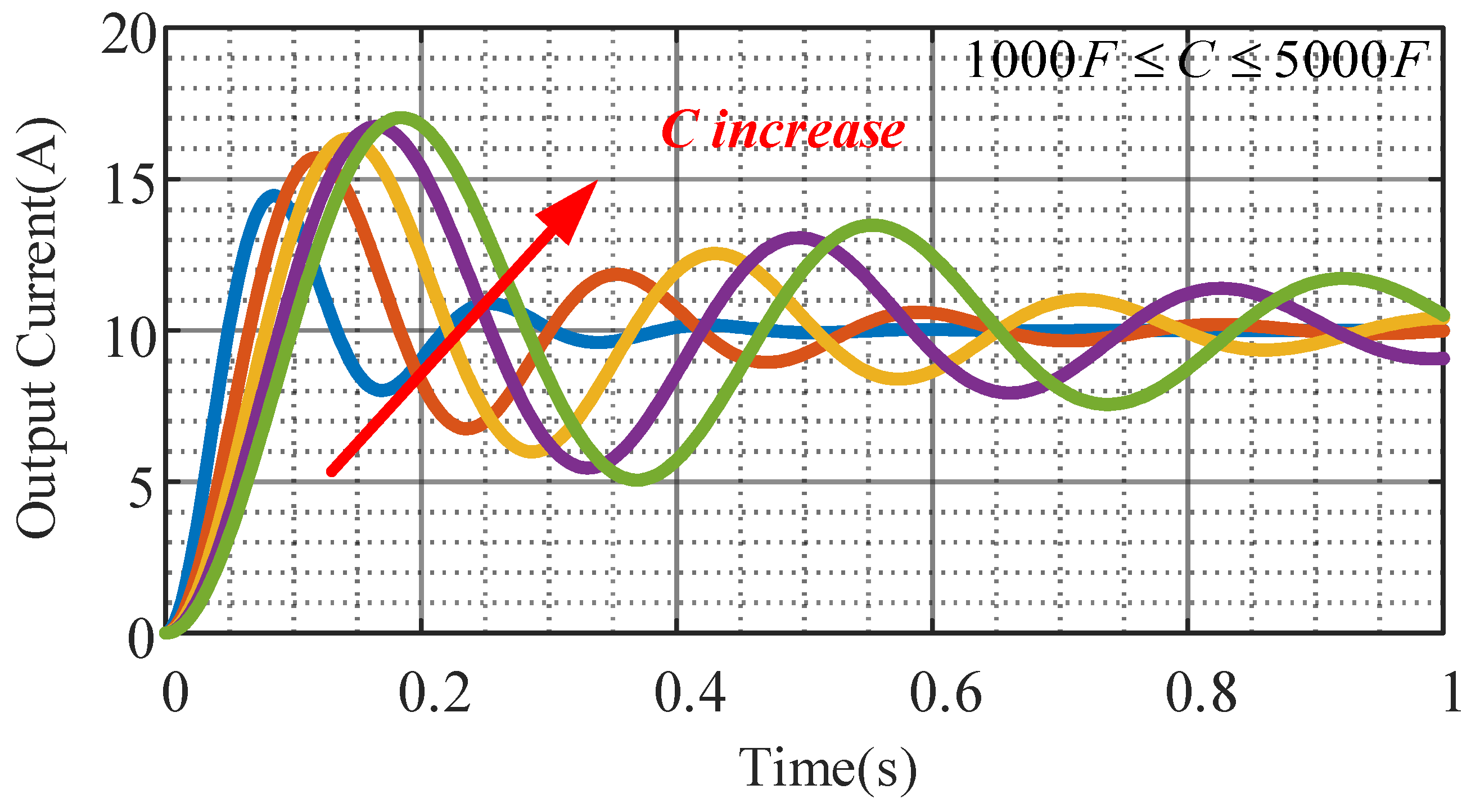
To further analyze the influence of the capacitor on the output voltage Uo of the VSG equivalent circuit model, Figure 10 presents the generalized root locus of the system with respect to the capacitance value, and Figure 11 shows the output current Io waveform of the VSG equivalent circuit model.
It can be observed from Figure 10 that when capacitance C = 0, the system has two poles, but one of them is at infinity; thus, there is only one effective pole. As capacitance C increases, the system transitions from an overdamped state to an underdamped state. It can also be found that reducing C can suppress the resonance of the VSG equivalent circuit model output current, but will cause the rate of change in the output voltage to exceed its allowed limit.
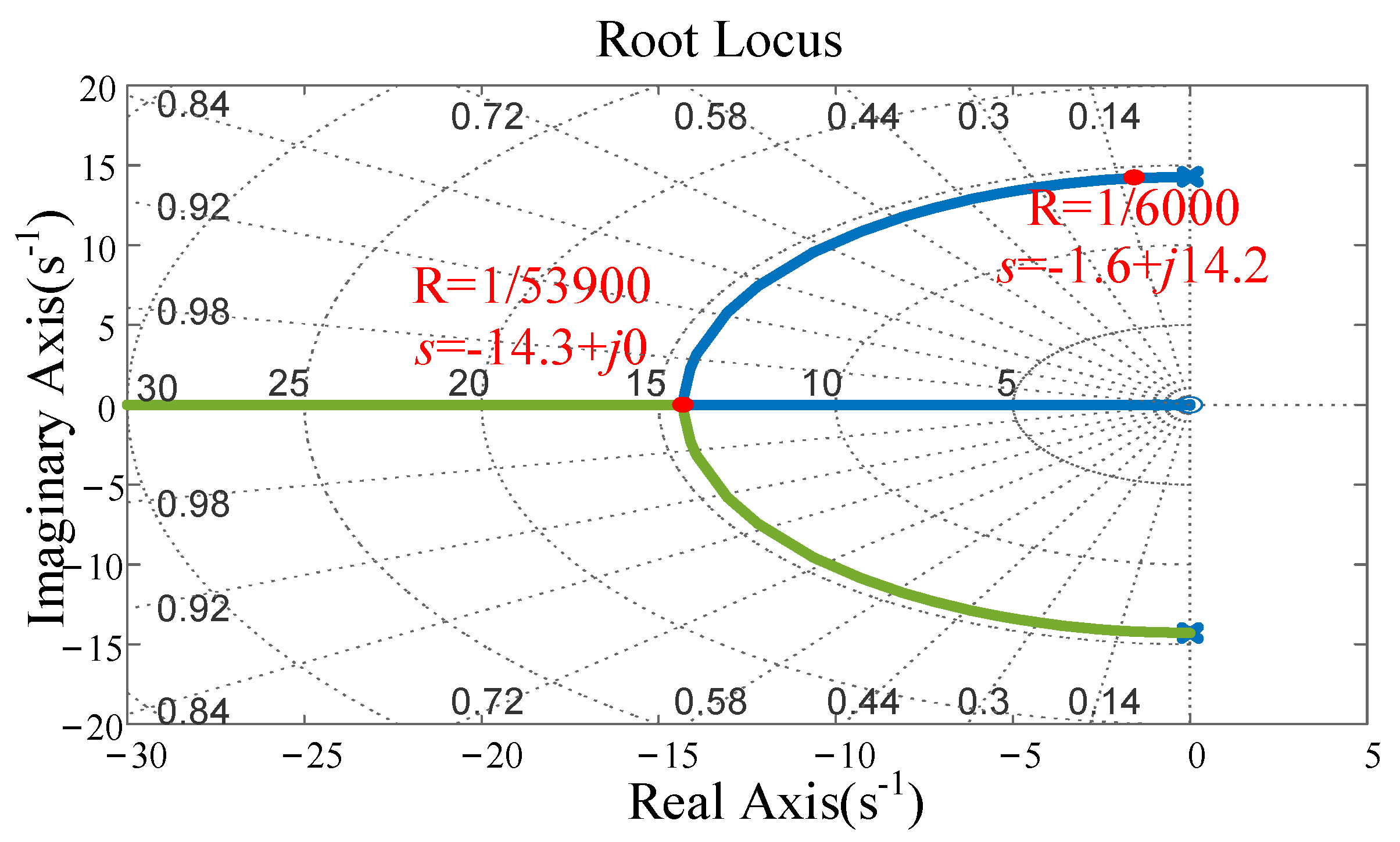
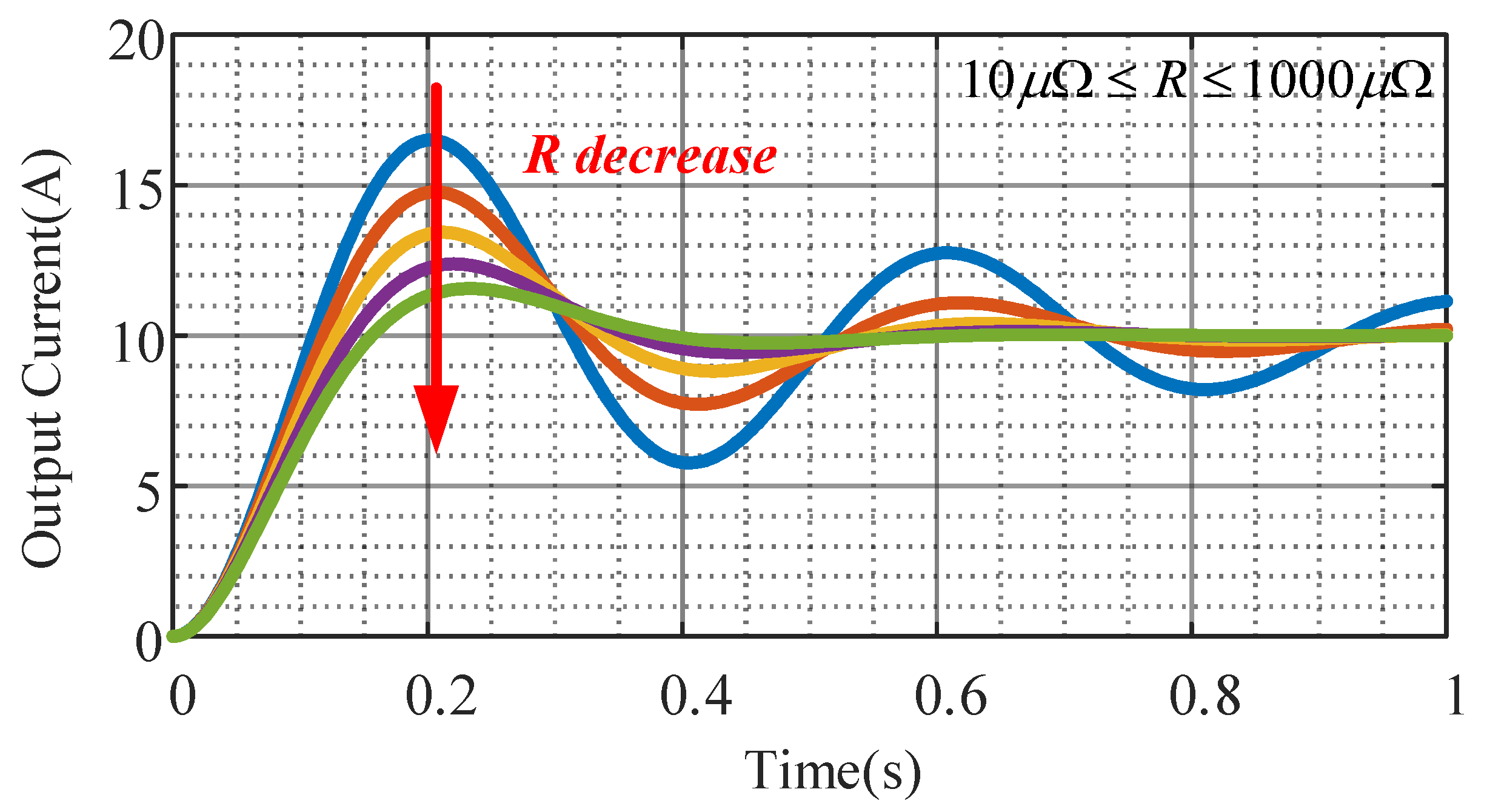
Next, to analyze the influence of the equivalent resistance on the output current Io, Figure 12 presents the generalized root locus of the system with respect to resistance, and Figure 13 shows the corresponding time-domain responses.
It can be observed that reducing resistance R increases the system damping ratio and suppresses output current resonance.
In summary, from the equivalent circuit perspective, increasing the capacitance in the VSG equivalent circuit reduces the rate of change in the output voltage, but it also worsens the resonance in the output current. Conversely, reducing the equivalent resistance can help suppress current resonance. However, these parameters cannot be arbitrarily selected, as they are constrained by the conditions of their equivalent VSG active power loop, such as the rate of change of frequency (ROCOF) and the power–frequency droop characteristics.

3.2. VSG Equivalent Circuit Parameter Constraints

From Equation (9), when the VSG participates in the grid’s primary frequency regulation, its active power output follows the droop characteristic, which can be expressed as
Δ P = Δ ω p c c D p = Δ ω g D p
According to Equation (15), when the droop coefficient is excessively large, even a slight disturbance in grid frequency can cause a significant variation in the VSG active power output, which may exceed its rated capacity.
In addition, when the VSG operates in the islanded mode, the droop coefficient determines the frequency deviation of the VSG output under load disturbances. Consequently, an excessively small droop coefficient will cause the VSG output frequency to exceed its allowable range even under light-load conditions. Therefore, the constraint of the droop coefficient can be expressed as
Δ P max 2 π Δ f = Δ P max Δ ω D p Δ P max Δ ω g = Δ P max 2 π Δ f g
Based on the equivalence to the VSG active power control, the range of resistance R in the equivalent circuit can be derived as
2 π Δ f g Δ P max R 2 π Δ f Δ P max
From Equation (9), when VSG operates in the grid-connected mode, the ROCOF of VSG is proportional to the power variation and inversely proportional to the virtual inertia. To ensure the ROCOF of VSG does not exceed the limit, the virtual inertia shall satisfy the following:
J Δ P max 2 π ω 0 λ
Similarly, through the corresponding relationship between VSG control parameters and the VSG equivalent circuit, the range of capacitance can be derived as
C Δ P max 2 π λ
Obviously, in the VSG equivalent circuit model, the R and C constraints defined by Equations (17) and (19) limit the extent of the resonance suppression achievable by parameter adjustment. Therefore, it is proposed that new damping branch can be added into the VSG equivalent circuit to further suppress the resonance.

4. Proposed Equivalent Damping Resistance Branch

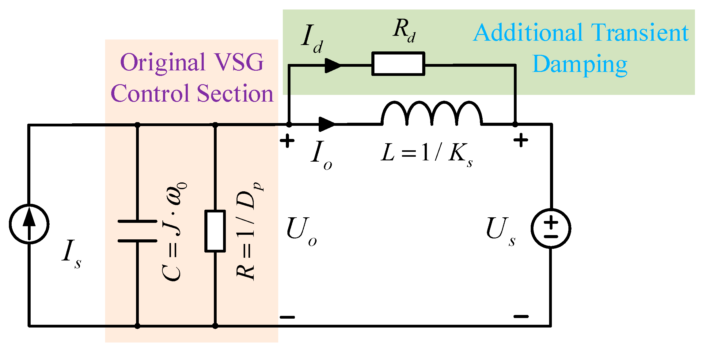
Intuitively, this paper proposes connecting a damping resistance branch in parallel with the inductor, as illustrated in Figure 14, where Rd provides damping for the output current resonance. When the VSG equivalent circuit reaches the steady state, the inductor L can be approximated as a short circuit. Therefore, this additional transient damping branch will not affect the steady-state value of the output current.
As shown in Figure 14, the current of this extra damping branch can be obtained as
I d = I o s L R d
According to Equation (20), the relationship between the output current Io and the output voltage Uo can be obtained as
U o ( s C + 1 / R ) = I s I o ( 1 + s L R d )
From Figure 8, the characteristic equation of the original VSG equivalent circuit model can be obtained as
C R L s 2 + L s + R = 0
The proposed damping branch provides additional damping only during the transient process, while it is shorted by the parallel inductor in steady state. Basically, the equivalent resistance of the VSG equivalent circuit model with the proposed damping branch during the transient period can be expressed as
R 0 = R R d R + R d
Also, the damping ratio of the VSG equivalent circuit with the proposed damping branch can be obtained as
ξ = R + R d 2 R R d C L
Herein, ξ = 0.707 is selected to achieve reasonable dynamic performance to achieve the critical damping ratio, which is usually used in the control system design to reach a balance between short settling times and low overshoots. Therefore, the damping resistor Rd can be derived from Equation (24) as
R d = R 2 ξ R C L 1
When a damping resistor Rd is introduced into the VSG equivalent circuit model, at the moment when Is changes, the capacitor in Figure 15 can be regarded as a short circuit. Therefore, the voltage across its terminals remains zero, and the output voltage Uo of the VSG equivalent circuit model remains unchanged. Is flows entirely through the capacitor. Then, the rate of change in the voltage across the capacitor (same as Uo) can be obtained as
d U o d t | t = 0 = 1 C i C ( 0 )
When the system is in steady state, the capacitor can be regarded as an open circuit and the inductor as a short circuit. Therefore, the expression for the output current of the equivalent circuit is
I 0 = I s
Equations (26) and (27) demonstrate that the proposed additional damping branch does not alter the original rate of change in the output voltage or the steady-state output current of the VSG equivalent circuit.
In the following analysis, the response characteristics of the output current Io are investigated to evaluate the effectiveness of the proposed damping branch. The transfer function of the output current Io with the proposed damping branch can be obtained as
T = R d R R d C L R s 2 + ( L R + R d L ) s + R d R
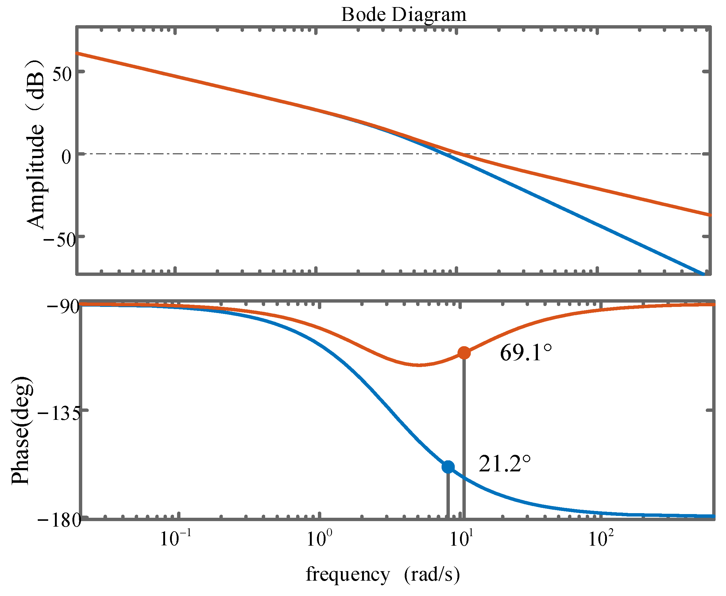
Figure 15 presents the Bode plot before and after adding the damping resistor branch.
As shown in Figure 15, the phase margin is only 21.2° before adding the damping branch, while the phase margin increases to 69.1° after adding the damping branch. Meanwhile, the cut-off frequency of the VSG equivalent circuit with the damping branch is much higher. Therefore, this proposed scheme not only achieves a faster response speed, but also significantly improves the dynamic performance and reduces system oscillations.
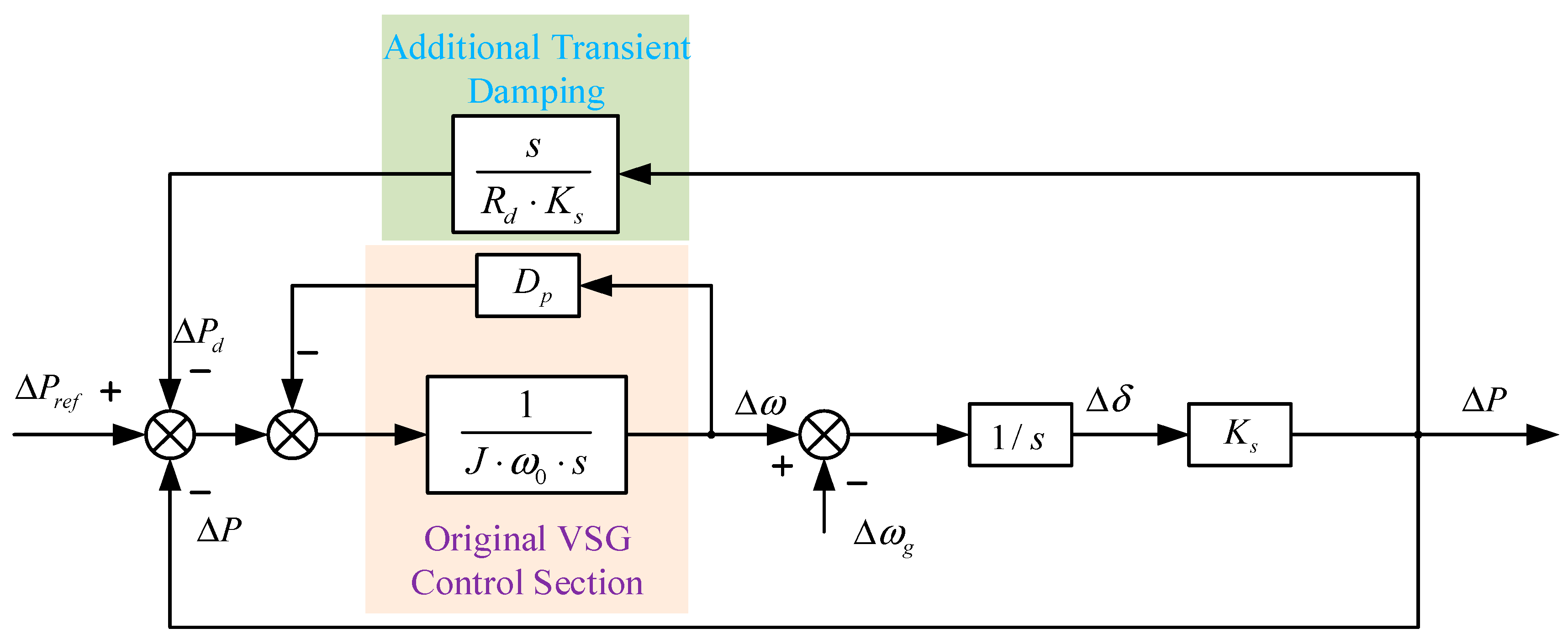
With all the prior straightforward equivalent circuit-based analysis and proposal, the actual VSG active power control loop can be revised, according to the corresponding relationship between the VSG equivalent circuit and the VSG active power loop.
Basically, Figure 14 can be converted to the new VSG active power control diagram as in Figure 16, where the additional damping branch in the circuit is equivalent to an extra power feedback loop in the VSG control loop.
Note that the VSG power control loop exhibits a very low bandwidth (≤10 Hz). As a result, the changes in VSG power loop have negligible impact on the converter’s equivalent harmonic output impedance [1]. Therefore, the equivalent damping branch-based controller addition does not introduce additional harmonic distortion nor degrade the output voltage quality [1].

5. Experimental Verification

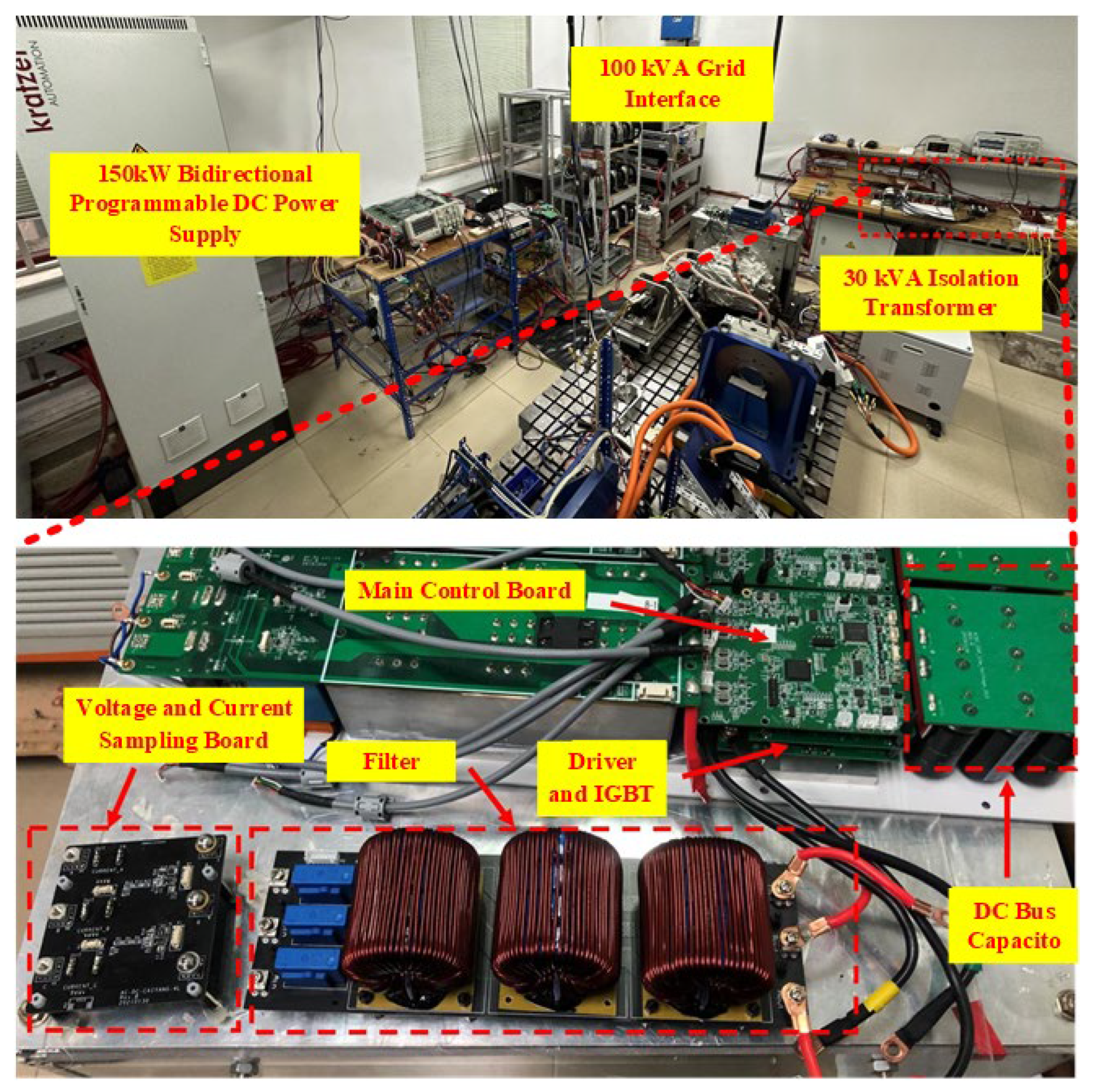
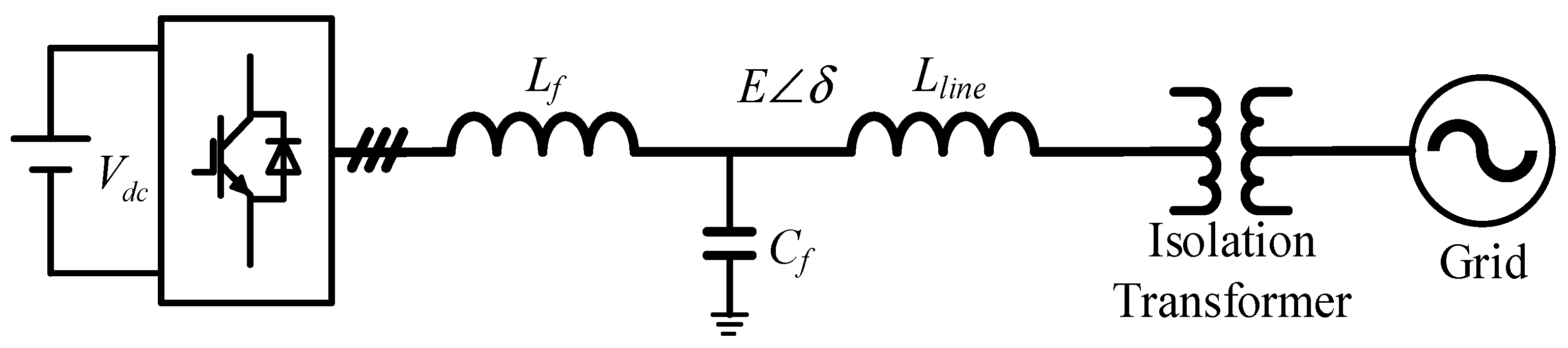
To verify the analysis of the dynamic characteristics of the VSG, as well as the effectiveness of the additional damping resistance branch in suppressing the power oscillation of the VSG, a 20 kVA prototype was built in the laboratory, as shown in Figure 17, and its simplified schematic diagram is presented in Figure 18.
Among them, the DC source is supplied by a 150 kW Kratzer high-voltage bidirectional DC programmable power supply, which is connected to the DC bus capacitor; the inverter part includes a three-phase inverter bridge module composed of IGBTs and an integrated LC filter module. The IGBT module is a 1200 V/150 A 39AC12T4V1 three-phase bridge module produced by Semikron (Nuremberg, Germany), and the driver module adopts the 2ED020I12-F2 chip manufactured by Infineon (Neubiberg, Germany); the line inductor is simulated by an external 1 mH inductor and connected to the power grid through a 20 kVA isolation transformer. All control programs are implemented by the TMS320F28335 DSP produced by TI (Dallas, TX, USA). Meanwhile, an oscilloscope is used to collect voltage and current signals during operation, while signals that are inconvenient to collect (such as frequency and power) are synchronized to the computer for display through CAN communication combined with the 2020 version of LabVIEW.
As reported in [28], an increase in line impedance can enhance the transient performance of VSG. As summarized in Table 2, the experiments in this study were conducted under relatively low line impedance, which makes the lab results more convincing in demonstrating the effectiveness of the proposed approach.
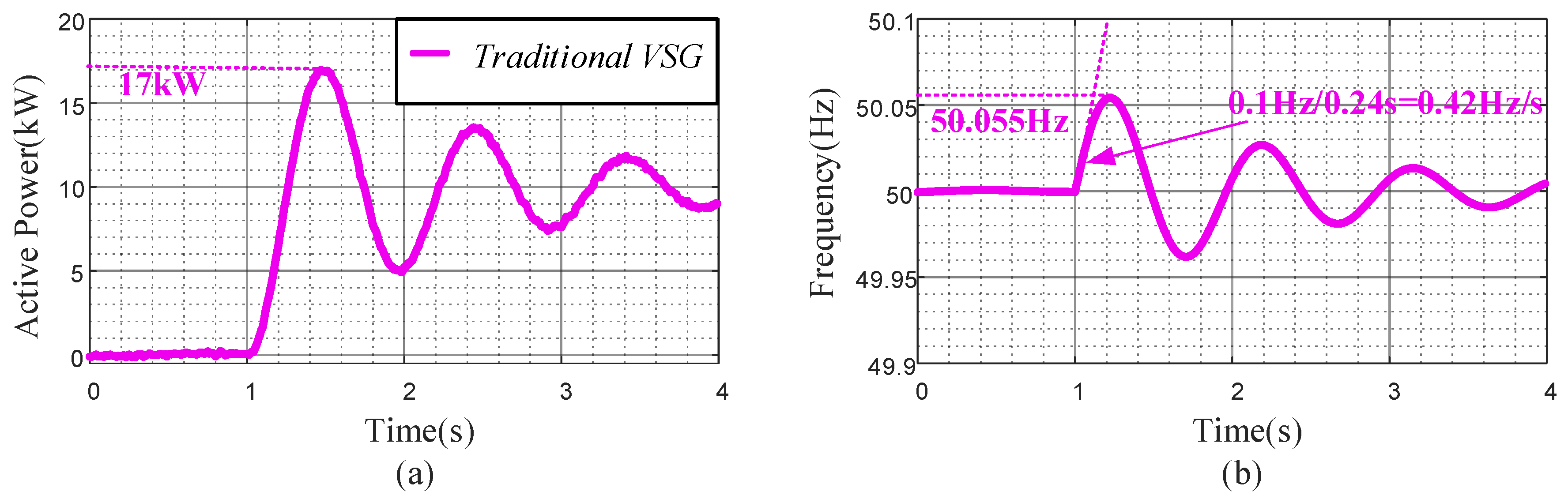
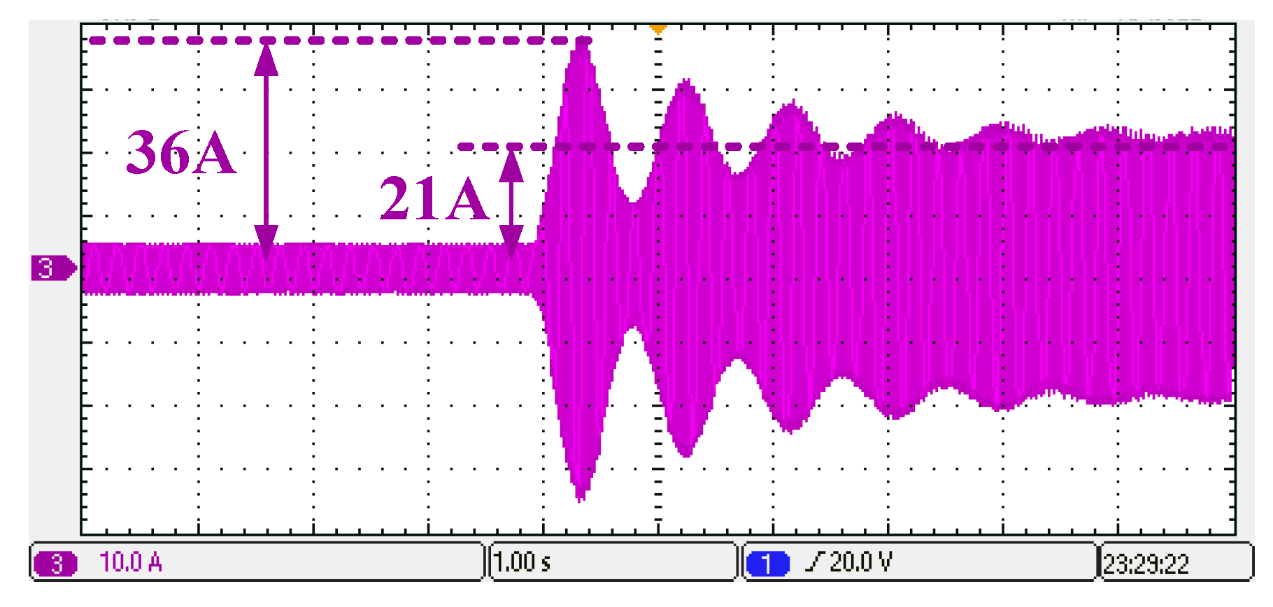
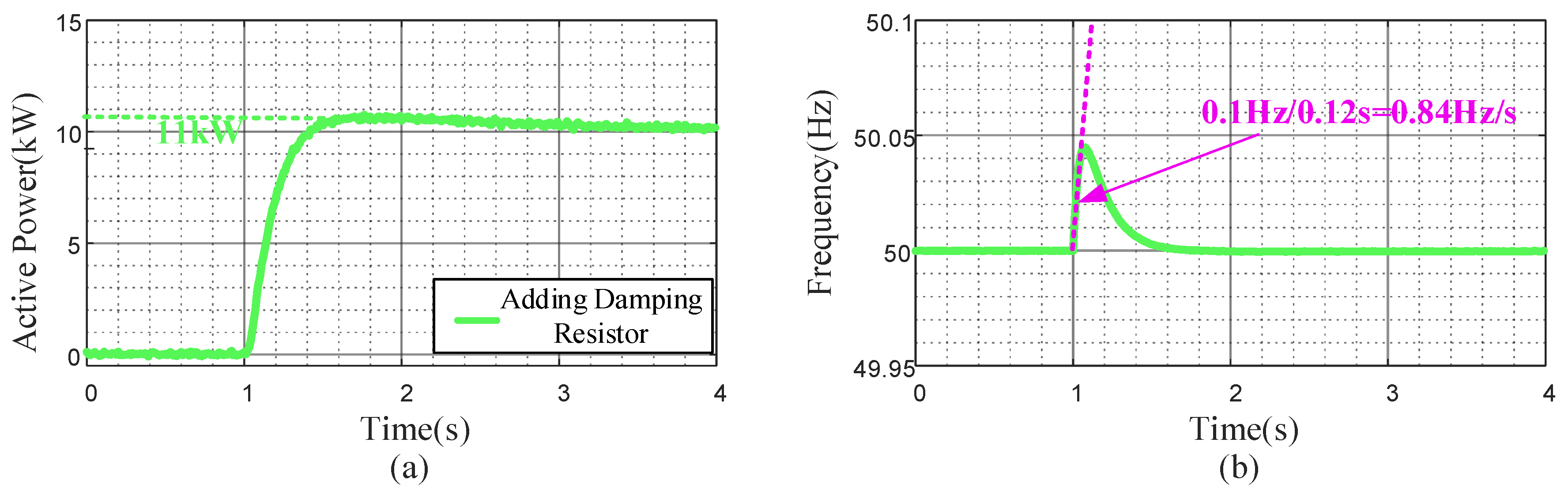
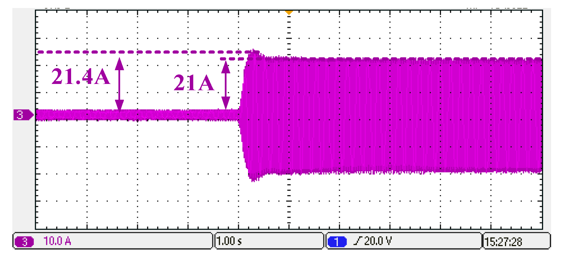
The experiment was conducted after the VSG was successfully connected to the power grid, with a 10 kW power step command issued. Figure 19 shows the grid-connected power and frequency oscillation of the traditional VSG, and Figure 20 presents the corresponding current waveform; Figure 21 demonstrates the suppression effect on the grid-connected power and frequency oscillation of the VSG after adding the damping resistor Rd branch, and Figure 22 shows the corresponding current waveform.
By comparing the power oscillations, frequency oscillations, and current waveforms of the traditional VSG with those of the VSG with the proposed damping resistor Rd branch, it is found that after adding the damping resistor Rd, the amplitude of the power oscillations is significantly reduced compared with that of the traditional VSG. The oscillation duration is also shortened, and both the amplitude and duration of the current waveform oscillations are decreased.

6. Conclusions

To mitigate the pronounced frequency and power oscillations of VSG under power command disturbances, this paper proposes a transient improvement strategy based on the equivalent circuit of the VSG active power loop. By establishing a physically interpretable equivalent circuit model, the analysis reveals that, under constraints of maximum frequency deviation and ROCOF, conventional parameter tuning only cannot achieve satisfactory damping performance. To overcome this limitation, an additional damping resistance branch is introduced into the VSG equivalent circuit, which directly enhances the system damping ratio and effectively suppresses frequency and power oscillations. Compared with complex, model-dependent suppression methods, the proposed approach offers clear physical insight, low design complexity, and strong engineering applicability. Finally, a high-power experimental platform is built for validation. Results confirm that with the proposed strategy the amplitude of power oscillations is reduced by more than 30%, the amplitude of frequency fluctuations by more than 25%, and the attenuation time of current oscillations by more than 40%. These results fully verify the method’s effectiveness in suppressing transient oscillations. Owing to its simplicity and ease of implementation, the proposed method shows strong potential for practical deployment in converter-based distributed generation systems, microgrids, and other emerging power electronic applications. In future work, the proposed equivalent circuit-based analytical method and the resulting oscillation suppression method will be further applied and investigated in systems with multiple VSG sources.

Author Contributions

Conceptualization, Y.L.; Methodology, M.P., H.L., G.H. and Y.L.; Software, Y.T.; Validation, M.P. and Y.L.; Formal analysis, H.L.; Investigation, M.P., H.B. and G.H.; Resources, Y.T.; Writing—original draft, Y.T., H.L., H.B. and G.H.; Project administration, H.B. All authors have read and agreed to the published version of the manuscript.

Funding

This work was funded by China Southern Power Grid Co., Ltd. Science and Technology Project (031300KK52222077).

Data Availability Statement

The original contributions presented in this study are included in the article. Further inquiries can be directed to the corresponding author.

Conflicts of Interest

Authors Mai Pan, Haili Liu and Guoqiang Huang were employed by the Huizhou Power Supply Bureau, China Southern Power Grid Co., Ltd. Authors Yingjie Tan, Hao Bai and Yipeng Liu were employed by the Electric Power Research Institute, China Southern Power Grid Co., Ltd. This work was funded by China Southern Power Grid Co., Ltd. Science and Technology Project. The authors declare that the research was conducted in the absence of any commercial or financial relationships that could be construed as a potential conflict of interest.

References

  1. Yang, B.; Li, H.; Shan, L.; Wei, L.; Lu, S. A Fundamental and Harmonic Frequencies Decoupled Control Scheme to Improve the Output Current Quality of Grid-Forming Inverters. IEEE Trans. Power Electron. 2024, 39, 15757–15769. [Google Scholar] [CrossRef]
  2. Yao, Z.; He, X.; Xiao, Z.; Deng, F.; Dai, C.; Lu, S.; Tang, Y. Current Ripple Prediction and ZVS-Based Variable Switching Frequency Control for Interleaved Multiphase Three-Level DC–DC Converter. IEEE Trans. Power Electron. 2025, 40, 5109–5119. [Google Scholar] [CrossRef]
  3. Wang, J.Y.; Hu, Y.W.; Zhang, K.; Yang, S.H.; Li, B.F.; Hao, Z.G. Dynamic Assessment of Voltage Support Capability of Grid-forming Converters Considering the Influence of Outer-Loop Control. South. Power Syst. Technol. 2025, 19, 1–8. [Google Scholar]
  4. Zhang, H.; Ruan, X.; Lin, Z.; Wu, L.; Ding, Y.; Guo, Y. Capacitor Voltage Full Feedback Scheme for LCL-Type Grid-Connected Inverter to Suppress Current Distortion Due to Grid Voltage Harmonics. IEEE Trans. Power Electron. 2021, 36, 2996–3006. [Google Scholar] [CrossRef]
  5. Wang, X.; Blaabjerg, F. Harmonic Stability in Power Electronic-Based Power Systems: Concept, Modeling, and Analysis. IEEE Trans. Smart Grid 2019, 10, 2858–2870. [Google Scholar] [CrossRef]
  6. Huang, W.; Zhai, S.; Lu, S.; Liu, Y.; Fang, Y.; He, W.; Zhu, D. Analysis of the Impact of Voltage Control on the Frequency Response Characteristics of Grid-Forming Converter. South. Power Syst. Technol. 2024, 18, 102–111. [Google Scholar] [CrossRef]
  7. Dos Santos Serra, A.W.; de Souza Ribeiro, L.A.; Savaghebi, M. Current Controller for LCL-Type Grid-Following Inverter with Active Damping and Capacitor Voltage Decoupling. In Proceedings of the IECON 2024—50th Annual Conference of the IEEE Industrial Electronics Society, Chicago, IL, USA, 3–6 November 2024; pp. 1–6. [Google Scholar] [CrossRef]
  8. Huang, Y.; Fang, Z.; He, Z.; Wang, D.; Tang, J.; Xie, C.; Zhou, K. Impacts of Interactions between Grid-Forming and Grid-Following Converters on Stability of Hybrid System Connected to Weak Grid. In Proceedings of the 2024 IEEE 7th International Electrical and Energy Conference (CIEEC), Harbin, China, 10–12 May 2024; pp. 2183–2188. [Google Scholar] [CrossRef]
  9. Ding, W.; He, C.; Geng, H.; Liu, Y. A Novel Lyapunov Function for Transient Synchronization Stability Analysis of Grid-Following Converters. IEEE Trans. Power Syst. 2025, 40, 3588–3591. [Google Scholar] [CrossRef]
  10. Zhang, H.; Zhao, X.; Zhang, Z.; Gong, Y. Study on the Influencing Factors of Impedance Stability of Island Microgrid with Grid-Forming and Grid-Following Converters. In Proceedings of the 2024 4th International Conference on Energy Engineering and Power Systems (EEPS), Hangzhou, China, 9–11 August 2024; pp. 596–600. [Google Scholar] [CrossRef]
  11. Zheng, K.; Luo, C.; Sun, Z.; Zhu, Y.; Yu, J. Impedance Network Modeling of GFL and GFM Converters System Considering AC/DC Couplings. In Proceedings of the 2024 The 9th International Conference on Power and Renewable Energy (ICPRE), Guangzhou, China, 20–23 September 2024; pp. 185–190. [Google Scholar] [CrossRef]
  12. Li, J.; Meng, Y.; Lu, J.; Sun, Y.; Yin, R.; Wang, S. Small-Signal Stability Analysis of Grid-Tied GFL/GFM VSCs System. In Proceedings of the 2024 IEEE International Conference on DC Technologies and Systems (DCTS), Zhuhai, China, 19–20 October 2024; pp. 1–6. [Google Scholar] [CrossRef]
  13. Wang, Z.; Guo, J.; Sun, Y.; Cao, W.; Si, Y. Key Factors Affecting the Oscillation Stability of GFL and GFM Energy Storage Cluster Grid-Connected Systems. In Proceedings of the 2024 4th International Conference on Electrical Engineering and Control Science (IC2ECS), Nanjing, China, 27–29 December 2024; pp. 1087–1092. [Google Scholar] [CrossRef]
  14. Guerrero, J.M.; Vasquez, J.C.; Matas, J.; de Vicuna, L.G.; Castilla, M. Hierarchical Control of Droop-Controlled AC and DC Microgrids—A General Approach Toward Standardization. IEEE Trans. Ind. Electron. 2011, 58, 158–172. [Google Scholar] [CrossRef]
  15. Vasquez, J.C.; Guerrero, J.M.; Savaghebi, M.; Teodorescu, R. Modeling, Analysis, and Design of Stationary Reference Frame Droop Controlled Parallel Three-Phase Voltage Source Inverters. In Proceedings of the 8th International Conference on Power Electronics—ECCE Asia, Hefei, China, 22–25 May 2016; pp. 272–279. [Google Scholar] [CrossRef]
  16. Vijay, A.S.; Dheer, D.K.; Tiwari, A.; Doolla, S. Performance Evaluation of Homogeneous and Heterogeneous Droop-Based Systems in Microgrid—Stability and Transient Response Perspective. IEEE Trans. Energy Convers. 2019, 34, 36–46. [Google Scholar] [CrossRef]
  17. Meng, X.; Liu, J.; Liu, Z. A Generalized Droop Control for Grid-Supporting Inverter Based on Comparison Between Traditional Droop Control and Virtual Synchronous Generator Control. IEEE Trans. Power Electron. 2019, 34, 5416–5438. [Google Scholar] [CrossRef]
  18. Pan, D.; Wang, X.; Liu, F.; Shi, R. Transient Stability of Voltage-Source Converters with Grid-Forming Control: A Design-Oriented Study. IEEE J. Emerg. Sel. Top. Power Electron. 2020, 8, 1019–1033. [Google Scholar] [CrossRef]
  19. Li, J.; Wen, B.; Wang, H. Adaptive Virtual Inertia Control Strategy of VSG for Micro-Grid Based on Improved Bang-Bang Control Strategy. IEEE Access 2019, 7, 39509–39514. [Google Scholar] [CrossRef]
  20. Alipoor, J.; Miura, Y.; Ise, T. Power System Stabilization Using Virtual Synchronous Generator with Alternating Moment of Inertia. IEEE J. Emerg. Sel. Top. Power Electron. 2015, 3, 451–458. [Google Scholar] [CrossRef]
  21. Hou, X.; Han, H.; Zhong, C.; Yuan, W.; Yi, M.; Chen, Y. Improvement of Transient Stability in Inverter-Based AC Microgrid via Adaptive Virtual Inertia. In Proceedings of the 2016 IEEE Energy Conversion Congress and Exposition (ECCE), Milwaukee, WI, USA, 18–22 September 2016; pp. 1–6. [Google Scholar] [CrossRef]
  22. Wang, F.; Zhang, L.; Feng, X.; Guo, H. An Adaptive Control Strategy for Virtual Synchronous Generator. IEEE Trans. Ind. Appl. 2018, 54, 5124–5133. [Google Scholar] [CrossRef]
  23. Qu, S.; Wang, Z. Cooperative Control Strategy of Virtual Synchronous Generator Based on Optimal Damping Ratio. IEEE Access 2021, 9, 709–719. [Google Scholar] [CrossRef]
  24. Li, D.; Zhu, Q.; Lin, S.; Bian, X.Y. A Self-Adaptive Inertia and Damping Combination Control of VSG to Support Frequency Stability. IEEE Trans. Energy Convers. 2017, 32, 397–398. [Google Scholar] [CrossRef]
  25. Huang, L.; Xin, H.; Yuan, H.; Wang, G.; Ju, P. Damping Effect of Virtual Synchronous Machines Provided by a Dynamical Virtual Impedance. IEEE Trans. Energy Convers. 2021, 36, 570–573. [Google Scholar] [CrossRef]
  26. Chen, M.; Zhou, D.; Blaabjerg, F. Active Power Oscillation Damping Based on Acceleration Control in Paralleled Virtual Synchronous Generators System. IEEE Trans. Power Electron. 2021, 36, 9501–9510. [Google Scholar] [CrossRef]
  27. Rathnayake, D.B.; Razzaghi, R.; Bahrani, B. Generalized Virtual Synchronous Generator Control Design for Renewable Power Systems. IEEE Trans. Sustain. Energy 2022, 13, 1021–1036. [Google Scholar] [CrossRef]
  28. Yang, B.; Li, H.; Xu, S.; Liu, H.; Lu, S. Systematic Methods to Eliminate the Transient Circulating Powers in the Multi-VSGs System. IEEE Trans. Smart Grid 2024, 15, 179–190. [Google Scholar] [CrossRef]
Figure 1. VSG control diagram.
Energies 19 01575 g001
Figure 2. Active power control loop of the VSG control.
Energies 19 01575 g002
Figure 3. Reactive power control loop of the VSG control.
Energies 19 01575 g003
Figure 4. Power transmission model of VSG.
Energies 19 01575 g004
Figure 5. The simplified small signal model of VSG.
Energies 19 01575 g005
Figure 6. The dynamic model of an RLC circuit.
Energies 19 01575 g006
Figure 7. RLC circuit schematics with VSG coefficients equivalence labels.
Energies 19 01575 g007
Figure 8. VSG equivalent circuit without the grid frequency disturbance equivalent voltage source.
Energies 19 01575 g008
Figure 9. Output voltage waveform of the VSG equivalent circuit model. (a) Global view. (b) Zoom-in detail.
Energies 19 01575 g009
Figure 10. Generalized root locus with respect to capacitance.
Energies 19 01575 g010
Figure 11. Output current waveforms for different capacitance.
Energies 19 01575 g011
Figure 12. Generalized root locus with respect to resistance R.
Energies 19 01575 g012
Figure 13. Output current waveforms with different resistances.
Energies 19 01575 g013
Figure 14. Equivalent circuit model with the proposed damping resistance branch.
Energies 19 01575 g014
Figure 15. Comparison of bode diagrams before and after adding the damping resistance branch.
Energies 19 01575 g015
Figure 16. Implementation of the proposed damping resistance branch.
Energies 19 01575 g016
Figure 17. Experimental platform.
Energies 19 01575 g017
Figure 18. Simplified schematic of experimental platform.
Energies 19 01575 g018
Figure 19. Oscillation of the traditional VSG. (a) Power oscillation. (b) Frequency oscillation.
Energies 19 01575 g019
Figure 20. Current waveform of the traditional VSG.
Energies 19 01575 g020
Figure 21. Suppression effect of the proposed damping resistance branch on VSG power oscillation. (a) Power oscillation. (b) Frequency oscillation.
Energies 19 01575 g021
Figure 22. Effect of the proposed damping resistor branch on VSG output current.
Energies 19 01575 g022
Table 1. The correspondence between the equivalent RLC circuit parameters and the parameters of the VSG active power loop.
Parameters in VSGParameters in Circuit
0C
1/DpR
1/KsL
PrefIs
PIo
ωUo
ωpccUs
Table 2. The parameters of the experimental prototype.
ParameterValue
DC Voltage Vdc/V700
Switching Frequency fs/kHz20
Filter Inductance Lf/μH400
Filter Capacitance Cf/μF30
Line Inductance L/μH1200
Rated Voltage E (RMS)/V220
Rated Frequency f/Hz50
Rated Power S/kVA10
Disclaimer/Publisher’s Note: The statements, opinions and data contained in all publications are solely those of the individual author(s) and contributor(s) and not of MDPI and/or the editor(s). MDPI and/or the editor(s) disclaim responsibility for any injury to people or property resulting from any ideas, methods, instructions or products referred to in the content.