1. Introduction
Power electronics systems play a critical role in aerospace applications, as they are responsible for ensuring the efficient control and distribution of electrical energy, e.g., within aircraft and spacecraft systems [
1]. In addition, such applications require power electronics with high power density to reduce weight and volume, which are crucial in space and aviation applications [
1]. Since power electronics for aerospace applications must operate in harsh conditions, enduring extreme temperatures, radiation, high voltage, high dv/dt, and high di/dt, they need to withstand these challenges without compromising performance [
2].
To reduce losses and increase the power delivered by the system, wide-bandgap (WBG) power semiconductor devices, such as GaN and SiC, are increasingly being employed, as they currently offer the highest level of technological maturity and component performance [
1]. In addition, a new generation of ultra-wide-bandgap (UWBG) semiconductors is under active development, including gallium oxide (Ga
2O
3) [
3], diamond [
4], aluminum nitride (AlN) [
5], and alloy systems based on AlGaN and InAlN [
6]. These materials will enable higher breakdown voltages, improved thermal management, and more compact and efficient power converters in the future.
WBG devices have considerable potential in aerospace applications and are increasingly used in electric propulsion systems, satellite power conversion, battery management, and power electronics, among others [
2]. The main applications of these devices in the aerospace sector are illustrated in
Figure 1 [
7].
WBG devices offer several advantages over conventional semiconductors, such as silicon (Si), including superior energy efficiency, the ability to operate at high temperatures and voltages, and robustness in harsh environments [
2]. In addition to efficiency advantages, WBG power devices exhibit superior properties that make them especially suitable for aerospace applications [
1]. One of the main advantages is their ability to operate at higher temperatures compared to traditional Si devices, allowing for consistent performance under adverse conditions. For example, SiC MOSFETs can operate at temperatures exceeding 200 °C, which not only improves efficiency but also reduces the need for complex and heavy cooling systems [
8]. WBG devices are also highly efficient in terms of switching, exhibiting significantly lower switching losses, which is crucial in applications where energy efficiency is vital, such as in aircraft power systems and spacecraft [
9]. Moreover, WBG devices have a remarkable ability to withstand high voltages and high rates of voltage and current variation. This makes them ideal for systems that require rapid response and high performance in dynamic and demandingI acknowledge this note. environments [
9]. However, the integration of these devices into existing systems and the development of new power conversion topologies also present technical and engineering challenges that require ongoing research [
10]. Despite their advantages, WBG devices are not without challenges; the long-term reliability of these devices under extreme conditions, such as prolonged exposure to radiation and thermal cycling, remains an active area of research [
11]. Issues related to production costs and implementation complexity also need to be addressed for these technologies to be adopted on a large scale in the aerospace industry [
12].
Aligned with these topics, the main contributions of this work are as follows: (i) to provide a structured and aerospace-oriented overview of WBG semiconductor materials, highlighting their main advantages, limitations, and integration challenges at both device and system levels; (ii) to present a consolidated discussion of key aerospace constraints, namely protection requirements, electromagnetic interference and compatibility (EMI/EMC), thermal management, and reliability, and to analyze their impact on power-converter design; (iii) to perform a comparative analysis of DC–DC and DC–AC power-conversion topologies commonly considered for aerospace platforms, with emphasis on design trade-offs rather than on the introduction of new topologies; (iv) to design and implement representative GaN-based DC–DC and DC–AC laboratory prototypes, which are experimentally evaluated under controlled conditions to provide functional validation and to illustrate practical implementation aspects and system-level integration trends enabled by WBG devices, without aiming at full aerospace qualification or optimized performance benchmarking.
2. Technological Challenges
Power electronics systems used in the aerospace sector face significant challenges that directly affect their efficiency, safety, and reliability. Although WBG devices such as SiC and GaN offer substantial performance improvements, their integration introduces new requirements in terms of protection, electromagnetic interference, thermal management, and fault tolerance.
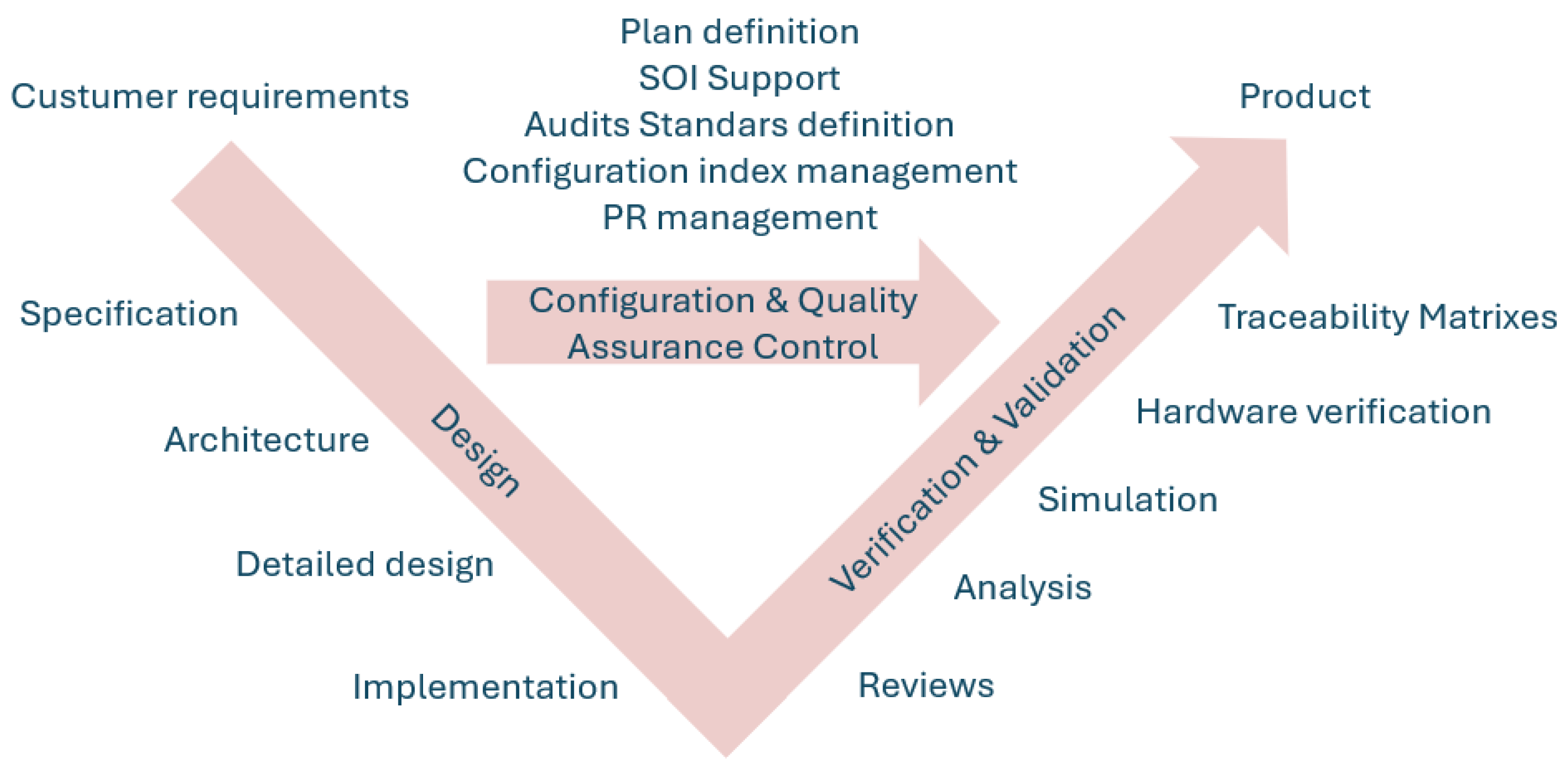
Figure 2, based on data from [
13], presents the V-Model used in the development and certification of safety-critical electronic systems, with emphasis on configuration management and quality assurance. This model is widely adopted in projects that follow strict standards such as DO-254 and DO-178C [
13], serving as a structured guide for the design, verification, and validation process. The left side of the figure represents the design stages, from requirements definition to implementation, while the right side focuses on verification and validation, ensuring that the system meets the established requirements.
2.1. General Protection
The high switching speed of WBG semiconductors leads to fast and high slew rate voltage (dv/dt) and current (di/dt) transitions in the power electronics converters. As a result, the likelihood of voltage and current spikes occurring during switching events increases. To limit these effects, fast-response protection algorithms capable of acting within microseconds are implemented to reduce fault current impact. In addition, the use of encapsulation materials with high thermal conductivity and reinforced insulation improves heat dissipation and increases the component’s tolerance to thermal variations [
14]. In aerospace systems, the integration of real-time monitoring and predictive diagnostics is essential to prevent failures, complemented by redundant protection mechanisms such as fast-acting fuses, circuit breakers, and fault-tolerant architectures that ensure continuous operation under extreme conditions [
15].
2.2. EMI/EMC
The fast-switching speed of WBG devices increases the emission of electromagnetic interference (EMI), which can compromise the performance of sensitive systems, making electromagnetic compatibility (EMC) a key factor in the design of electronic systems for aerospace applications [
16]. Reducing this problem requires a careful design approach focused on minimizing parasitic inductances through optimized PCB layouts, implementing differential filters to limit conducted and radiated emissions, and applying spread-spectrum modulation techniques that distribute interference energy over a wider frequency range. Despite recent advances, electromagnetic interference remains one of the main challenges for the integration of GaN-based technologies in aerospace platforms, even though these devices can significantly reduce the mass and volume of power systems [
17].
2.3. Temperatures
Temperature is one of the most critical factors in the aerospace environment. Although SiC and GaN devices can operate at temperatures above 200 °C, it is essential to ensure the thermal stability of the system in order to maintain performance and extend its operational lifetime [
18]. Considering the weight and space constraints inherent to this type of application, passive cooling strategies are often preferred. These include high-efficiency heat sinks, liquid circulation systems, and materials with high thermal conductivity, thus avoiding the need for more complex and heavier active cooling solutions [
17].
2.4. Reliability
Reliability is a critical aspect of aerospace power systems, which must ensure continuous operation under extreme conditions of temperature, voltage, and radiation. Although WBG devices offer superior performance, they remain susceptible to degradation mechanisms associated with excessive temperature, electrical instability, and prolonged radiation exposure. High-Temperature Operating Life (HTOL) tests, thermal cycling, and radiation tolerance evaluations are essential for assessing the long-term behavior of these devices [
19]. The HTOL test subjects electronic components to high temperature and electrical stress over an extended period, effectively simulating years of real-world operation within a short timeframe. This accelerated aging process helps identify potential failure mechanisms and estimate the operational lifetime of the device, providing valuable insights into its performance under aerospace conditions [
20]. The adoption of advanced packaging techniques and predictive monitoring strategies further enhances system durability and reduces the likelihood of in-mission failures.
2.5. Fault Tolerance
Fault-tolerant design is a crucial requirement in aerospace power systems, where continuous and safe operation must be guaranteed even in the presence of component faults or system anomalies. The objective of fault-tolerant systems is to maintain partial or full functionality after a failure occurs, preventing critical mission interruptions. To achieve this, redundancy strategies, both hardware and control-based, are commonly implemented [
21]. Hardware redundancy includes the duplication of critical components such as switches, sensors, or control circuits, enabling automatic reconfiguration in case of failure. Control-based redundancy, on the other hand, involves advanced algorithms capable of fault detection, isolation, and compensation through real-time monitoring and adaptive control techniques [
22]. In systems employing WBG devices, the implementation of fault-tolerant mechanisms becomes even more relevant due to their high switching speeds and susceptibility to transient stresses. Fast fault-detection circuits can significantly reduce damage propagation and improve recovery time [
23].
3. Power Electronics Technologies
Power electronics technologies play a key role in enabling efficient power conversion across a wide range of aerospace applications, including mobility systems and renewable energy generation. Improving the efficiency of the most used power electronics converters depends on several factors, including the selection of materials for the specific technologies of power electronics components.
3.1. Semiconductors
WBG-based devices are a crucial step toward achieving this goal, offering excellent performance when faced with extreme operating conditions such as high temperatures, switching frequencies, and voltages [
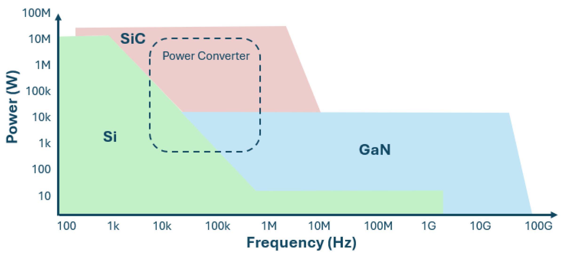
24]. A decisive characteristic is also their usually very compact size. Within these wide bandgap technologies, GaN and SiC emerge as the leading materials due to their superior performance characteristics. In
Figure 3, using data from [
25], a comparison is presented between the power and operating frequency of various semiconductor technologies, highlighting the superiority of SiC and GaN materials over Si.
Complementing this analysis,
Table 1 presents a comparison of the main technological properties of the Si, SiC, and GaN semiconductors. This comparison provides a clearer understanding of the structural and functional differences between these technologies, highlighting the advantages of WBG materials in applications that require high efficiency, enhanced thermal robustness, and superior switching performance.
SiC diodes can be classified into three different categories: (i) SiC Schottky diode; (ii) SiC p-i-n diode; and (iii) SiC merged p-n-Schottky diode (MPS) or junction barrier Schottky diode (JBS) [
26]. SiC Schottky diodes are widely used due to their negligible reverse recovery current and very high switching speed, and are commercially available with breakdown voltages typically above 600 V, depending on the target application. SiC p-i-n diodes, on the other hand, have significant reverse recovery current, a relevant disadvantage. However, a key benefit is that they provide low conduction losses under high current conditions. JBS diodes merge SiC Schottky efficiency with SiC p-i-n robustness, achieving low conduction loss and high voltage blocking [
26].
Currently, the SiC transistor market provides two main types of devices: vertical MOSFETs and cascode-configured vertical JFETs [
27]. As an example of a discrete SiC MOSFET, devices such as the C3M0065100K offer low switching losses and high-voltage capability, making them suitable for compact high-efficiency converters. Although SiC devices came out earlier, GaN power transistors entered the market approximately a decade later [
27]. GaN high-electron mobility transistors (HEMTs) are among the most used GaN devices in power electronics, thanks to their high efficiency and fast switching capabilities. A disadvantage usually associated with these devices is their normally ON characteristic, which can pose safety concerns in power systems that require a guaranteed shutdown in case of failure. A common way around this is to use a cascode configuration, which makes the device behave as if it is normally OFF [
27]. An example of such GaN devices is the NV6128 [
28], a high-performance GaN power IC that integrates a GaN HEMT and driver in a single package, enabling fast switching and simplified gate-drive design. Additionally, discrete GaN HEMTs without integrated drivers are also widely available, such as the GS66508T [
29], which provides high switching speed and low losses while requiring an external gate driver.
In addition to these discrete devices, there are also SiC power modules that integrate multiple transistors into a single package, increasing the overall power capability and simplifying converter design. These modules can adopt different internal topologies, ranging from single-MOSFET configurations, such as the GCMX008C120S1-E1 [
19], to half-bridge modules like the FF2MR12KM1H [
30], or even full-bridge modules such as the MSCSM120TAM16TPAG [
31]. The use of such modules enables the implementation of compact converters with improved thermal efficiency and enhanced performance in high-power applications.
Table 2 presents the intrinsic properties of Si, SiC, and GaN semiconductors, highlighting the advantages of GaN, namely its high electron mobility and superior breakdown field, while SiC stands out due to its higher thermal conductivity [
32].
Despite its technical advantages, the adoption of GaN is still more limited compared to SiC. This is mainly due to its higher manufacturing costs, its lower level of industrial development, and its reduced availability in higher-power ranges. However, studies indicate that replacing Si IGBTs with GaN transistors in 5 kW DC–AC inverters can reduce system weight by up to 50% and increase efficiency by around 5%, particularly under partial-load conditions [
32]. Moreover, the lower heat generation of GaN devices reduces the need for bulky heatsinks, contributing to more compact and efficient designs. Despite these current limitations, GaN is expected to play an increasingly important role in the development of high-efficiency power-conversion systems, enabling lighter, more compact, and more sustainable architectures [
33].
3.2. Capacitors
With the rise of WBG device technologies, power systems are being pushed to operate at much higher frequencies. This shift drives the need for high-frequency components across the board. Despite this demand, it is often overlooked the limitations of traditional, large DC-link capacitors [
34]. There are several types of capacitors, each suited to different applications depending on factors like capacitance, voltage rating, size, and stability: ceramic, electrolytic, and film.
High-frequency capacitors are designed with key performance objectives to ensure efficient operation in demanding applications, including the following: they must withstand high operating temperatures, have high-temperature dielectric materials, and be able to dissipate heat generated by semiconductor components [
35]. They must also support high current levels without compromising reliability and achieve low equivalent series resistance (ESR). One example of high-frequency capacitors is the TDK B25640 series, which is currently under development [
36]. The temperature limit for common film capacitors with standard polypropylene dielectric is +105 °C, while these TDK film capacitors can be used in temperatures up to 125 °C and have a rated operating voltage of 700–2200 V [
37].
3.3. Inductors
With the advancement of WBG device technologies, power systems are operating at increasingly higher frequencies. This evolution significantly raises the demands placed on magnetic components, particularly inductors, which must maintain stable performance under high-frequency, high-current, and high-temperature conditions. Despite this growing need, the limitations of traditional inductors, often based on ferrite cores and conventional windings, become evident in extreme environments such as aerospace applications [
38].
The inductors used in these systems must exhibit low equivalent series resistance (ESR), support high current levels, minimize magnetic losses, and ensure high thermal stability without compromising reliability. Moreover, they must withstand vibration, radiation, and significant temperature variations. A representative technology that meets these requirements is the Vishay SGIHLP series, recognized as the first IHLP
® inductor series qualified to MIL-STD-981 Class S for aerospace applications [
39]. These inductors are designed for high-current converters and noise-filtering applications, operating reliably up to +180 °C, with inductance values ranging from 0.22 µH to 100 µH and rated currents up to approximately 100 A, depending on the model [
40].
4. Power Electronics Converters
Aerospace applications demand power electronics converters with high efficiency, low weight, and high-power density while maintaining compliance with strict reliability and electromagnetic interference standards. Considering the limitation of using extremely advanced power electronics converters for aerospace applications (e.g., more critical when requiring redundant systems), the commonly used topologies include DC–DC converters (such as buck and boost), DC–AC inverters, and AC–DC rectifiers.
4.1. DC–AC and AC–DC Power Converters
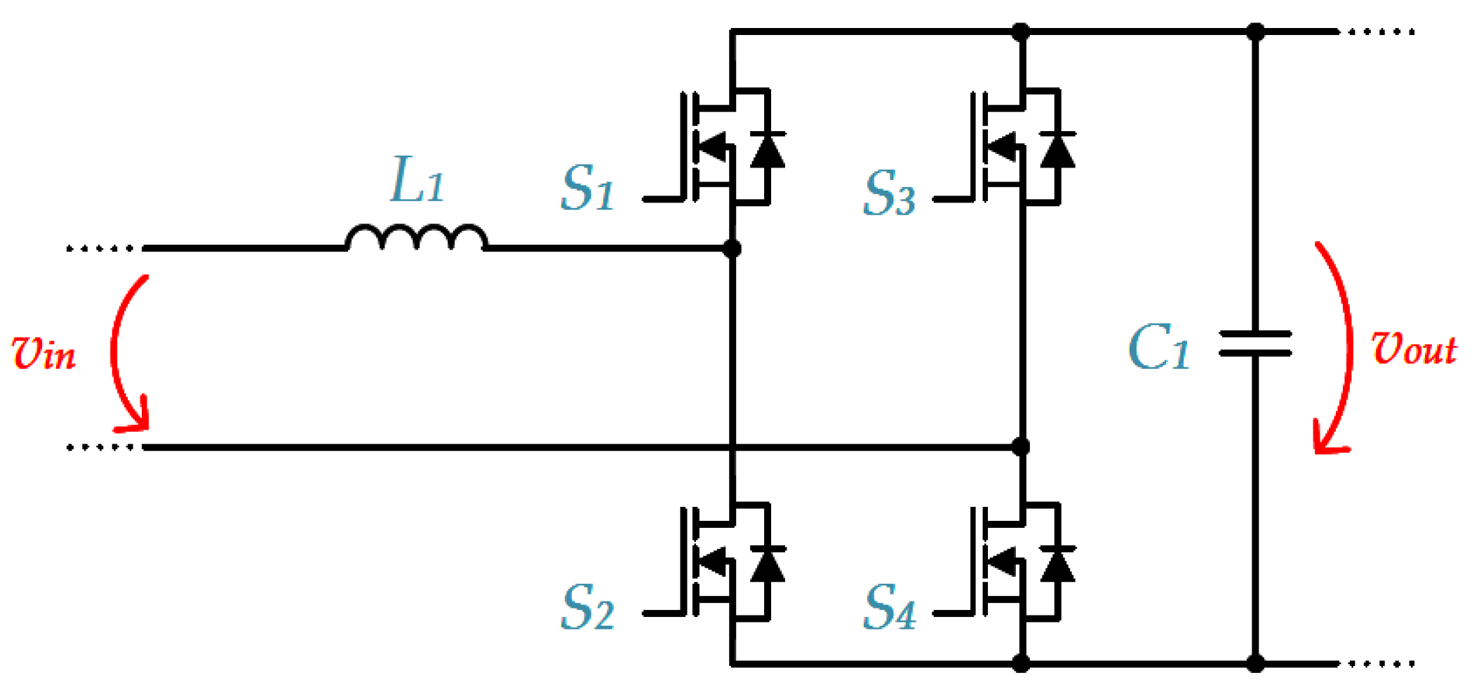
The power electronics converter presented in
Figure 4 is based on a single-phase full-bridge topology, designed to convert a DC voltage source into a single-phase AC output [
41]. It incorporates four semiconductor switches (e.g., SiC) arranged in two pairs that operate in a complementary manner to generate the AC output waveform. The capacitors (
C) stabilize the DC input voltage, ensuring a steady power supply, while the inductors (
L) smooth the AC output current, reducing harmonic distortion and protecting the load from sudden current variations.
This topology enables bidirectional operation, meaning that the power electronics converter can function both as an inverter and as an active rectifier, depending on the control strategy employed. When operating in inverter mode, the converter transforms a DC voltage source into a single-phase AC output with controlled frequency and amplitude. In aerospace power systems, this configuration can be used in low-power motor drives, the interface of renewable energy systems, and traction vehicles [
41]. In rectifier mode, the converter converts a single-phase AC input into a regulated DC output. This operation mode is essential for battery charging systems, onboard power supplies, and other applications where high efficiency and power quality are required [
41]. The efficiency and compact design of these converters make them a key technology in modern power conversion systems.
4.2. DC–DC Power Converters
DC–DC converters play a key role in aerospace applications by regulating voltage levels within onboard power distribution networks, conditioning battery systems, and interfacing with renewable sources such as solar photovoltaic arrays. The use of WBG devices enhances their performance by enabling higher switching frequencies, improved thermal behavior, and increased overall efficiency.
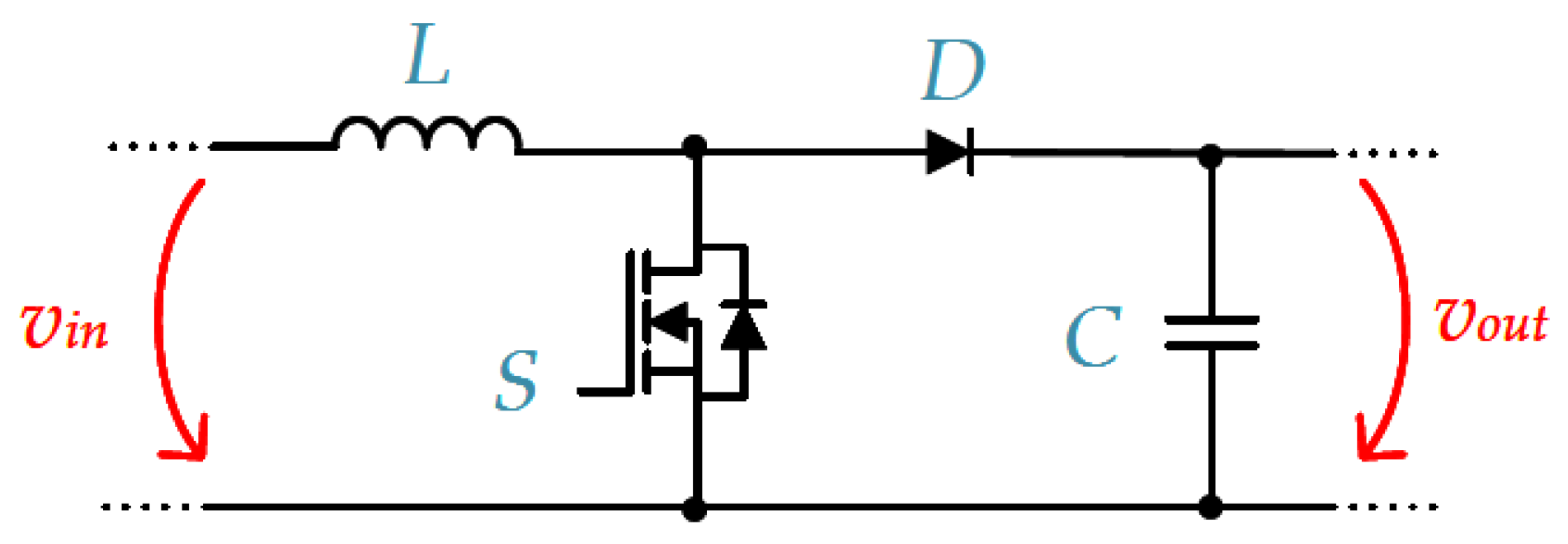
The DC–DC buck converter illustrated in
Figure 5 is often used in aerospace systems to step down high DC voltages to lower levels using a switching semiconductor, a diode (
D), an inductor (
L), and a capacitor (
C). When the switch is on, current flows through the inductor, storing energy while supplying the load. When the switch turns off, the inductor maintains the current flow through the diode, ensuring a continuous output. It is widely used, its applications including, for example, stepping down DC voltage from connected solar photovoltaic modules or energy storage systems to provide stable power to loads [
42].
A DC–DC boost converter is essential for stepping up low DC voltages to higher levels, commonly used in battery-powered systems and solar photovoltaic modules, as illustrated in
Figure 6. When the switch is on, current flows through the inductor (
L), storing energy. When the switch turns off, the inductor releases this energy, adding to the input voltage and supplying a higher output through the diode (
D) and capacitor (
C) [
43].
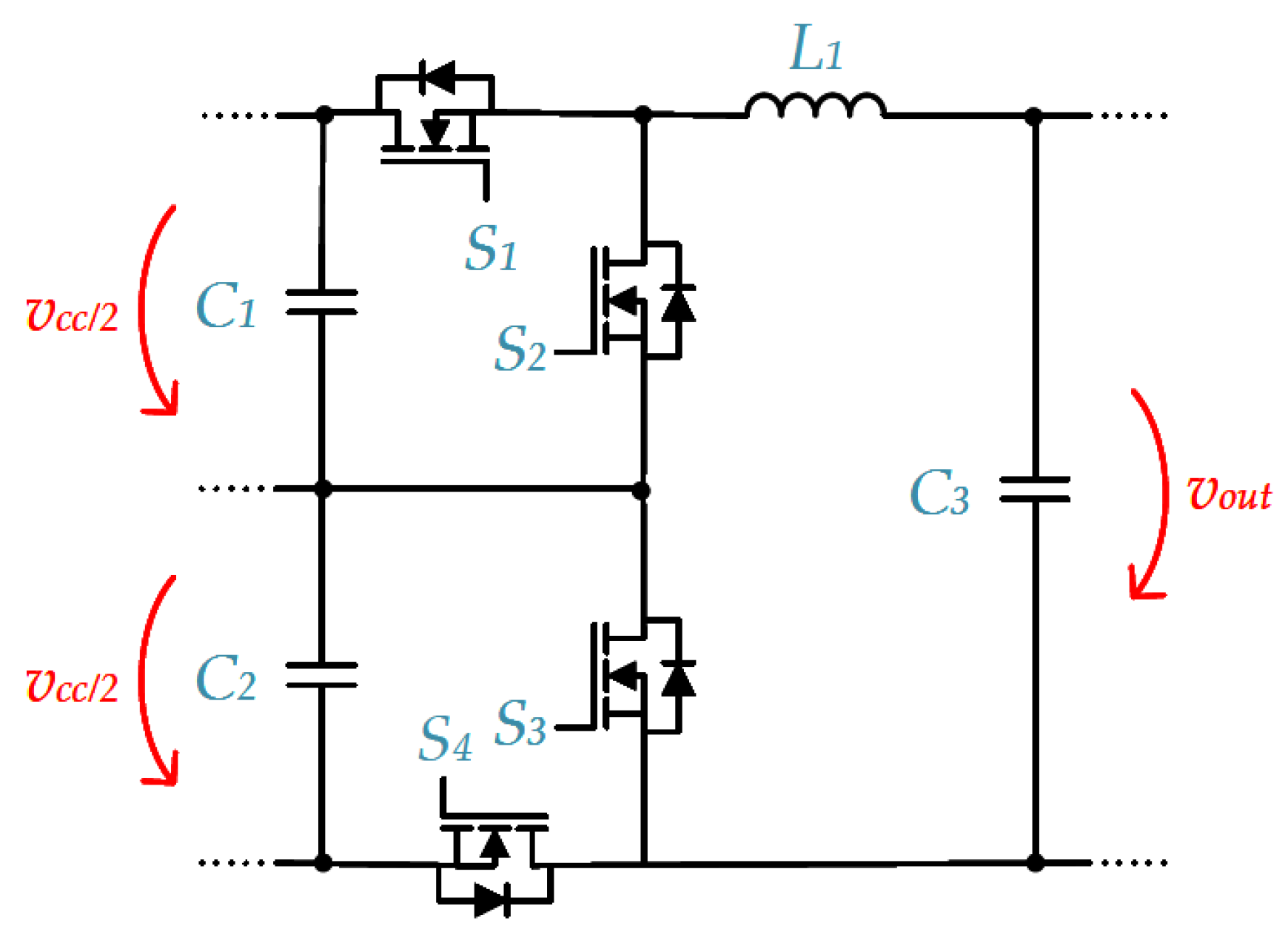
The three-level bidirectional DC–DC buck-boost converter (BB3L), shown in
Figure 7, represents an advanced evolution of traditional DC–DC converter topologies, offering enhanced performance for modern energy systems. This converter can operate in both buck (step-down) and boost (step-up) modes, while also enabling bidirectional power flow. Such flexibility makes it particularly well-suited for applications using battery energy storage systems, vehicles, and renewable energy integration. The inclusion of a three-level structure brings several advantages compared to conventional two-level counterparts: three possible distinct voltage levels at the output or input of the converter reduce voltage stress on switching devices. Therefore, the use of smaller passive components is possible, contributing to a more compact design. The bidirectional capability is achieved by using a symmetrical arrangement of active switches. The operating principle is based on: if the switches
S1 and
S4 are ON, then the converter is operating in the buck mode; if the switches
S2 and
S3 are ON, the converter is in the boost mode [
44].
The full-bridge LLC topology is a widely adopted solution in high-efficiency DC–DC converters, known for its soft-switching capability and excellent performance in medium- and high-power applications. This converter incorporates four switches (
S1,
S2,
S3, and
S4), an input capacitor (
C1), an output capacitor (
C3), four rectifier diodes (
D1,
D2,
D5, and
D4), a resonant capacitor (
C2), a resonant inductor (
L1), and the magnetizing inductor of the transformer (
L2). Unlike conventional converters that rely primarily on PWM techniques, where the duty-cycle of the switching signals is modulated to regulate the output voltage, LLC resonant converters employ a control strategy based on frequency modulation. This control strategy allows the converter to operate at high switching frequencies. As a full-bridge converter, illustrated in
Figure 8, the switches operate in pairs: if
S1 and
S4 are ON,
S2 and
S3 are OFF [
45].
Table 3 presents a comparison of the key characteristics of the different DC–DC converter topologies analyzed, providing a clear overview of their functionalities, control complexity, and operational limitations.
Although the comparison presented in
Table 3 is intentionally qualitative, it highlights key design trade-offs that are particularly relevant in aerospace-oriented power conversion. Classical two-level buck and boost converters are generally associated with high efficiency and simple control, but they impose higher voltage stress on the switching devices. Multilevel structures, such as the three-level bidirectional buck–boost (BB3L) converter, can mitigate device voltage stress and current ripple, contributing to improved efficiency and reliability, at the expense of increased control complexity and component count. Full-bridge LLC converters are widely recognized for their high-efficiency potential enabled by soft-switching operation; however, this performance comes with higher design complexity and tighter component tolerances. These trade-offs directly influence component stress, thermal behavior, and overall system reliability, which are critical considerations in aerospace power electronics design.
5. Implemented Power Electronics Converters
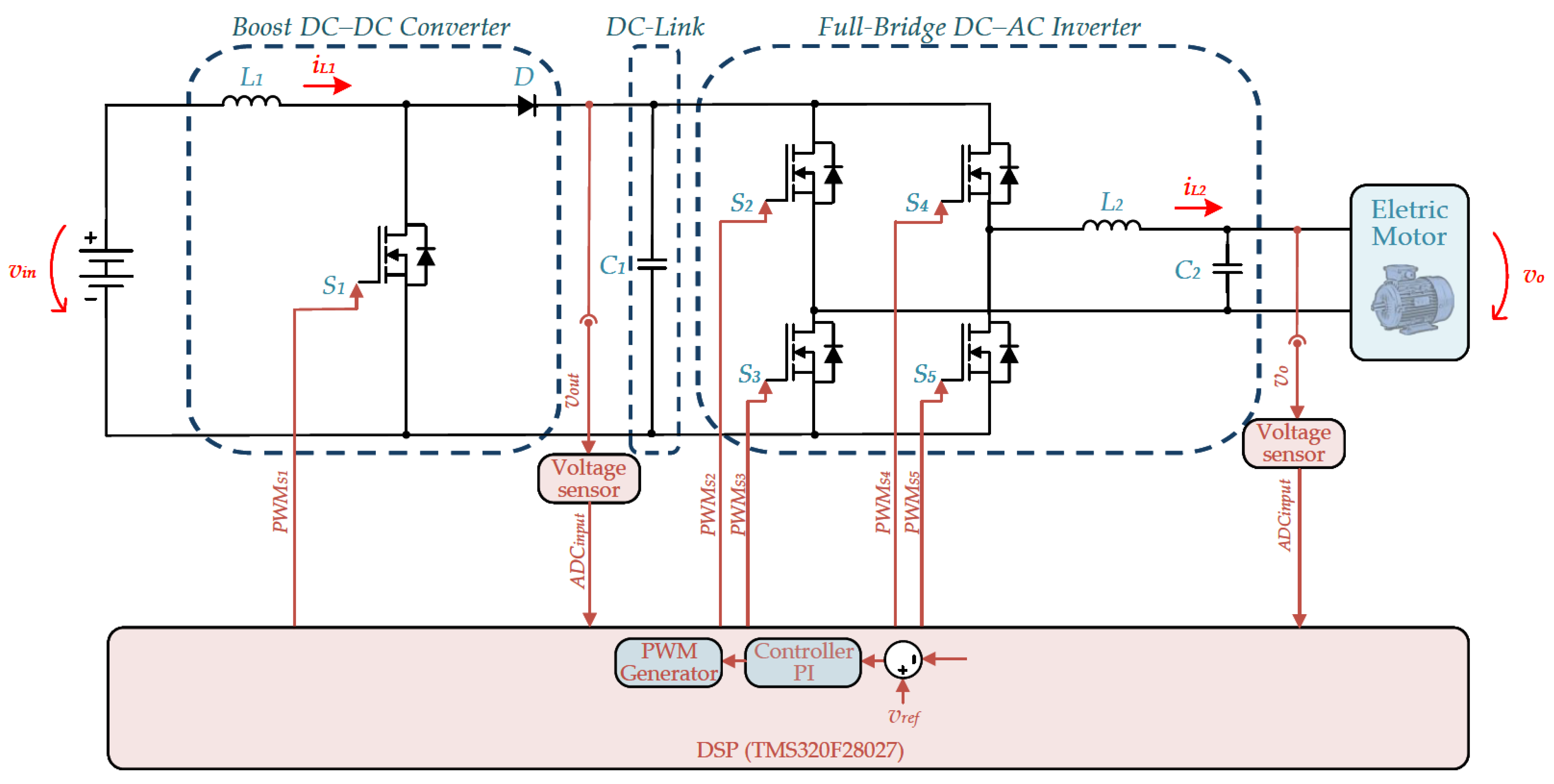
Following the previous analysis of SiC and GaN semiconductor technologies, as well as the study of power electronics converter topologies most suitable for aerospace applications, a representative laboratory implementation of power conversion prototypes was carried out. The main objective was to test these emerging WBG device technologies in functional laboratory-scale prototypes, evaluated under controlled laboratory conditions. Thus, it was possible to experimentally validate the concepts presented in the previous chapters and to assess their performance under representative operating conditions. Two power converters were considered, a DC–DC boost converter and a DC–AC single-phase full-bridge inverter, which are integrated to form a complete DC–AC conversion system.
5.1. Experimental Implementation of a GaN-Based Final Prototype
The developed system integrates two main power conversion stages, a DC–DC boost converter and a DC–AC full-bridge inverter. The architecture was implemented with the objective of converting the energy supplied by a battery to supply an AC load, representing a typical functional scenario in aerospace-oriented power systems, where it is necessary to step up the voltage to ensure the appropriate operating level.
To monitor the system behavior and implement control, voltage sensors were integrated at critical points of the circuit. The first sensor was placed at the output of the DC–DC boost converter, allowing the measurement of the output voltage (vout) and ensuring that the voltage level supplied to the full-bridge inverter is appropriate. The second sensor was installed at the inverter output, measuring the voltage (vo) applied to the load.
The use of these sensors enables real-time monitoring of the system’s critical variables, providing essential information to the digital controller responsible for adjusting the PWM signal of the semiconductor devices. This ensures stable operation and voltage regulation under different load conditions.
Figure 9 presents the complete schematic diagram of the power conversion system.
Table 4 presents the set of components used throughout the entire development process, i.e., both in the DC–DC boost and DC–AC full-bridge converters, thereby including all electronic materials employed in the conversion system.
5.2. Experimental Implementation of a GaN-Based DC–DC Boost Converter
To evaluate the performance of GaN semiconductors under realistic operating conditions, an experimental prototype of a DC–DC boost converter was developed. This circuit allows the assessment of critical operating parameters such as switching speed, power losses, and system stability prior to integration into the final DC–AC converter prototype.
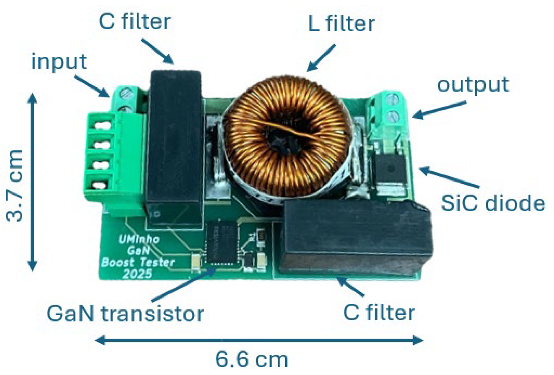
The power stage of the DC–DC boost employs the GaN NV6128 device, which integrates a transistor and its gate driver within a single compact package. The device is powered by a DC laboratory power supply and is switched by a PWM signal generated by the LAUNCHXL-F28027F microcontroller, enabling a detailed analysis of the dynamic behavior and efficiency of the GaN devices under various operating conditions.
Figure 10 shows the developed prototype, highlighting its compact design and optimized component layout, which contributes to reduced size and improved electrical performance of the converter.
Figure 11 presents experimentally measured waveforms obtained with an input voltage of 30 V, a switching frequency of 75 kHz, and a resistive load of 100 Ω. The figure shows the gate-drive signal and the corresponding voltage and current waveforms, highlighting the PWM switching process and the converter’s response. The average current measured at the load was approximately 0.9 A, corresponding to an output voltage of around 60 V across the 100 Ω resistor, which is consistent with the voltage-boosting function of the converter under the tested conditions. The observed waveforms demonstrate stable operating behavior, with a ripple level compatible with the switching frequency and the characteristics of the components used.
Under laboratory test conditions, the DC–DC boost converter achieved a maximum efficiency of approximately 97%. This value was obtained from the ratio between the measured output power and the input power, using experimental steady-state voltage and current measurements with a resistive load. The result demonstrates the high efficiency potential of GaN-based power converters, even in intermediate stages of prototype development.
5.3. Experimental Implementation of a GaN-Based DC–AC Full-Bridge Inverter
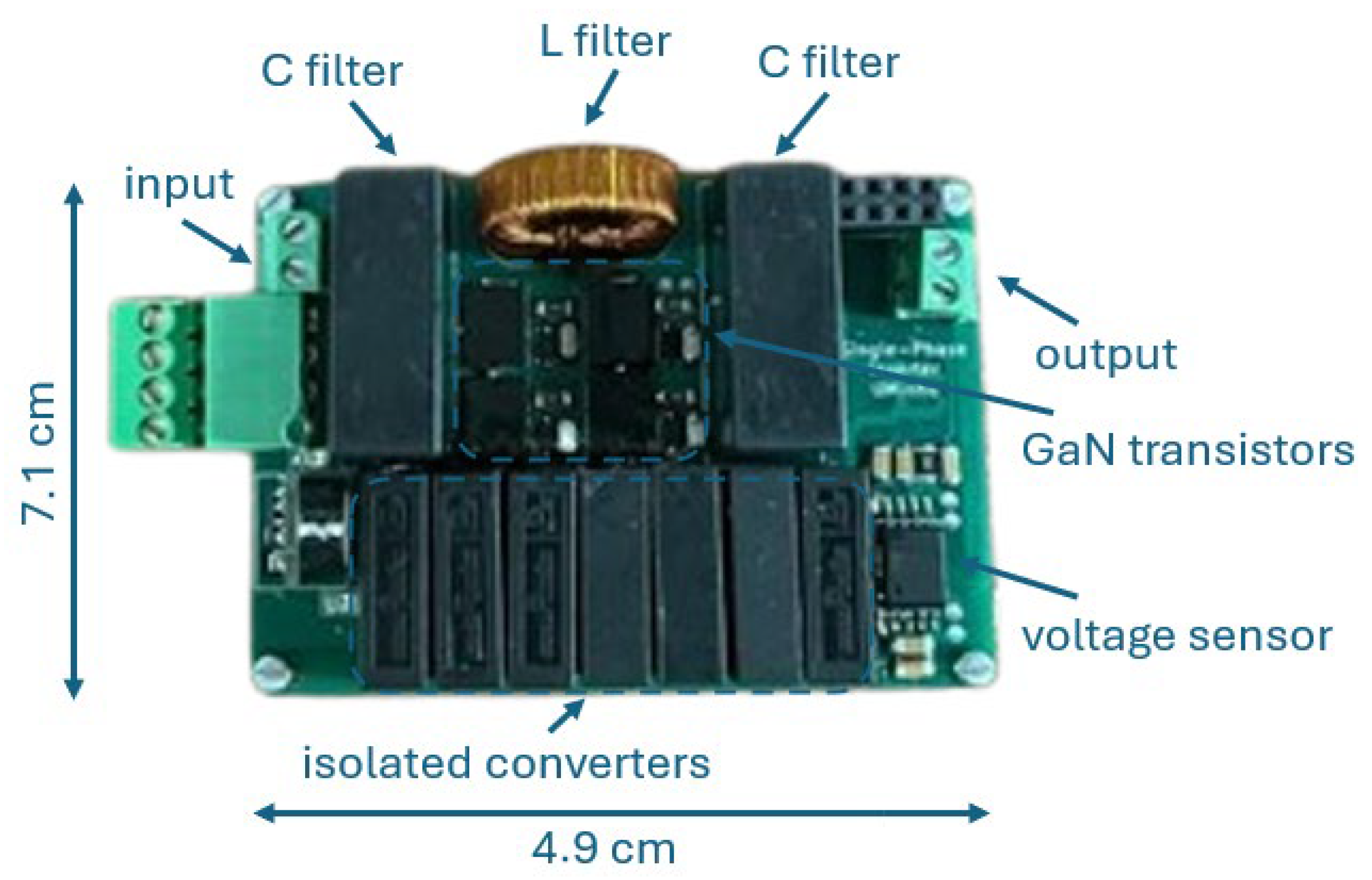
After validating the DC–DC boost converter, a single-phase DC–AC full-bridge inverter was developed. This configuration was chosen for its widespread use in power systems and its ability to operate efficiently at high switching frequencies. The
NV6128 device, the same GaN semiconductor used in the boost stage, was employed in this implementation due to its fast-switching capability, low on-resistance, and high efficiency, which contribute to optimizing the overall system performance.
Figure 12 shows the developed prototype, where the four switching devices, the filtering circuit, and the interface connectors can be observed.
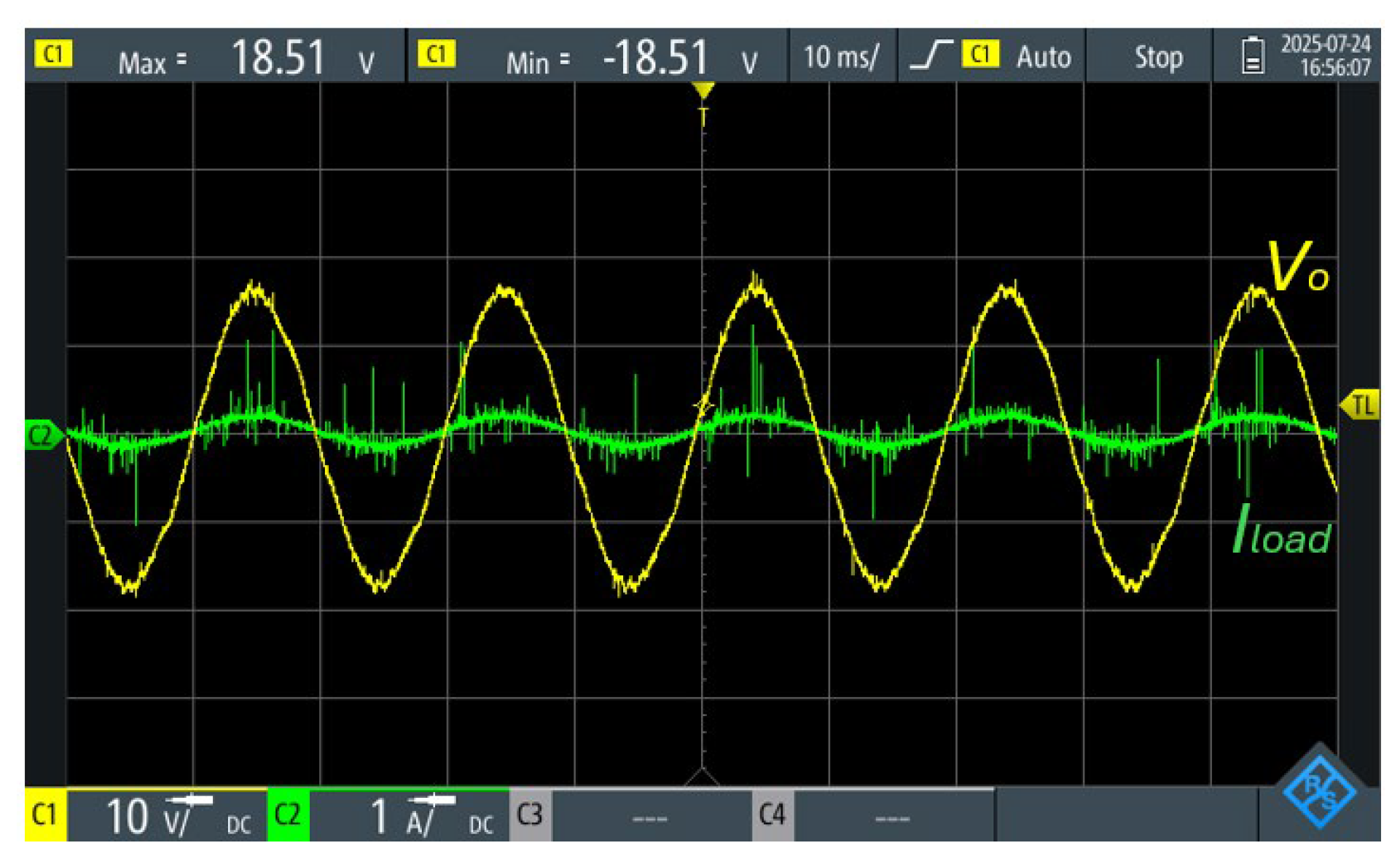
Figure 13 presents the experimental waveforms measured at the output of the full-bridge converter during open-loop operation with a resistive load. Both the voltage and current on the AC side of the load can be observed, demonstrating the generation of a sinusoidal alternating voltage from the DC input. This result validates the correct operation of the full-bridge topology and confirms the effectiveness of the implemented sinusoidal modulation strategy. It can also be seen that the voltage and current waveforms are in phase, which confirms the resistance of the load and the proper synchronization between both signals, thereby demonstrating the stability and consistency of the system’s operation under the tested conditions.
Under the same laboratory testing conditions, the DC–AC full-bridge inverter reached efficiency values around 95%. The slightly lower efficiency compared to the boost stage is mainly attributed to intermediate hardware modifications introduced during testing, namely the addition of anti-parallel diodes on the PCB, which increase parasitic elements and may contribute to additional switching-related losses.
6. Future Perspectives
Future perspectives in the field of power electronics based on WBG devices indicate significant progress at the levels of materials, conversion architectures, and control methodologies. Although GaN and SiC technologies have already demonstrated promising results, a wide range of research topics continues to shape the next generation of high-performance power systems for aerospace applications. One of the most relevant research directions concerns the development of UWBG semiconductors, such as Ga
2O
3, AlN, and diamond, which are expected to overcome the thermal and electrical limitations of current WBG materials. Their advancement involves critical challenges, including effective doping strategies, scalable epitaxial growth, and heterogeneous integration with GaN and SiC technologies, paving the way for even more compact converters with superior blocking capabilities [
46].
In parallel, significant progress is expected in epitaxial growth techniques and defect-engineering methods, strongly supported by artificial intelligence algorithms capable of optimizing growth parameters, predicting defect formation, and enhancing crystal quality at large scale. The integration of Industry 4.0 principles is also expected to play a decisive role in transitioning these technologies from research environments to industrial manufacturing [
46]. From the perspective of power converter design, future research will likely focus on high-frequency architectures, multilevel topologies, resonant converters, and high-power-density bidirectional structures, particularly relevant for electric propulsion, energy storage, and onboard generation modules in the aerospace sector [
47]. Advances in control algorithms will also be essential, with emphasis on predictive control, real-time robust control, and compensation methods for intrinsic non-idealities of WBG devices. Finally, challenges associated with reliability, thermal management, electromagnetic compatibility, and fault tolerance will remain central research areas. The development of advanced packaging, materials with enhanced thermal conductivity, EMI-mitigation techniques, and redundant architectures designed for extreme environments will be crucial to achieving certification and ensuring the safe use of these technologies in aerospace platforms [
48]. Overall, future perspectives in this scientific domain point to continuous progress in materials, processes, converter topologies, and control strategies, reinforcing the role of WBG and UWBG technologies as key enablers of the next generation of high-efficiency, high-reliability power-conversion systems.
7. Conclusions
WBG technologies, particularly SiC and GaN, are increasingly positioned as key enablers of the next generation of aerospace power-conversion systems. Their high efficiency, ability to withstand extreme temperatures, and superior electrical robustness address core requirements in aircraft and spacecraft, where weight, volume, and reliability are critical constraints. Although challenges remain, namely in protection design, electromagnetic compatibility, thermal management, and long-term reliability, the continuous evolution of materials, device structures, and converter architectures is steadily mitigating these limitations. In this context, WBG devices provide clear advantages at the converter level, enabling higher switching frequencies and increased power density when compared to conventional Si-based solutions.
Within this work, a laboratory-scale GaN-based DC–DC boost converter and a DC–AC full-bridge inverter were designed, implemented, and experimentally evaluated under controlled conditions. The laboratory implementation confirmed correct and stable operation of both conversion stages, including voltage boosting, high-frequency switching, and sinusoidal DC–AC conversion using commercially available WBG devices. The experimental results provide first-order validation of functional performance, efficiency trends, and waveform stability, which are relevant indicators for aerospace-oriented power-electronics development.
It is important to note that the experimental validation presented in this paper is not intended to represent aerospace qualification or mission-level verification. Instead, the results aim to illustrate practical implementation aspects, system-level integration considerations, and the performance potential enabled by WBG technologies at an intermediate stage of hardware development, prior to extended testing under aerospace-specific environmental and reliability constraints.
UWBG materials are expected to further enhance device blocking capability, thermal robustness, and performance in harsh environments. These technological developments are likely to support more compact, higher-frequency, and fault-tolerant power-conversion solutions tailored to aerospace demands. Overall, the findings highlight a clear direction: the future of aerospace power electronics will be shaped by WBG, and progressively UWBG, devices, combined with converter topologies optimized for high power density and with control strategies aligned with aerospace certification requirements, enabling the effective exploitation of the unique capabilities of these emerging semiconductor technologies.

