


A Method for Optimizing Turn-Off Losses Design in Parallel MOSFETs Inverter with RC Snubber Circuits



Abstract
1. Introduction
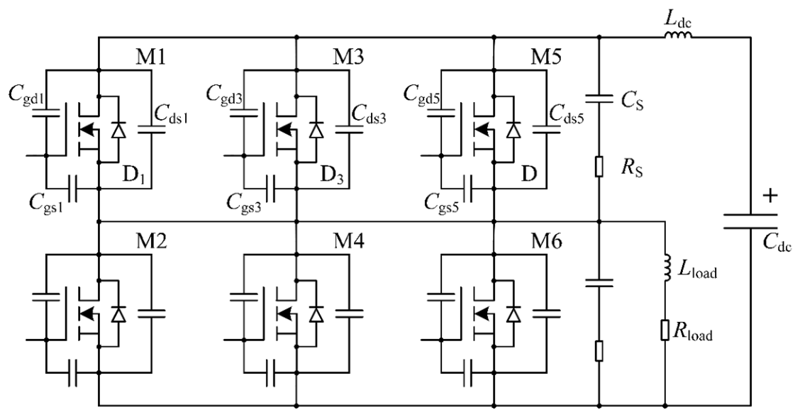
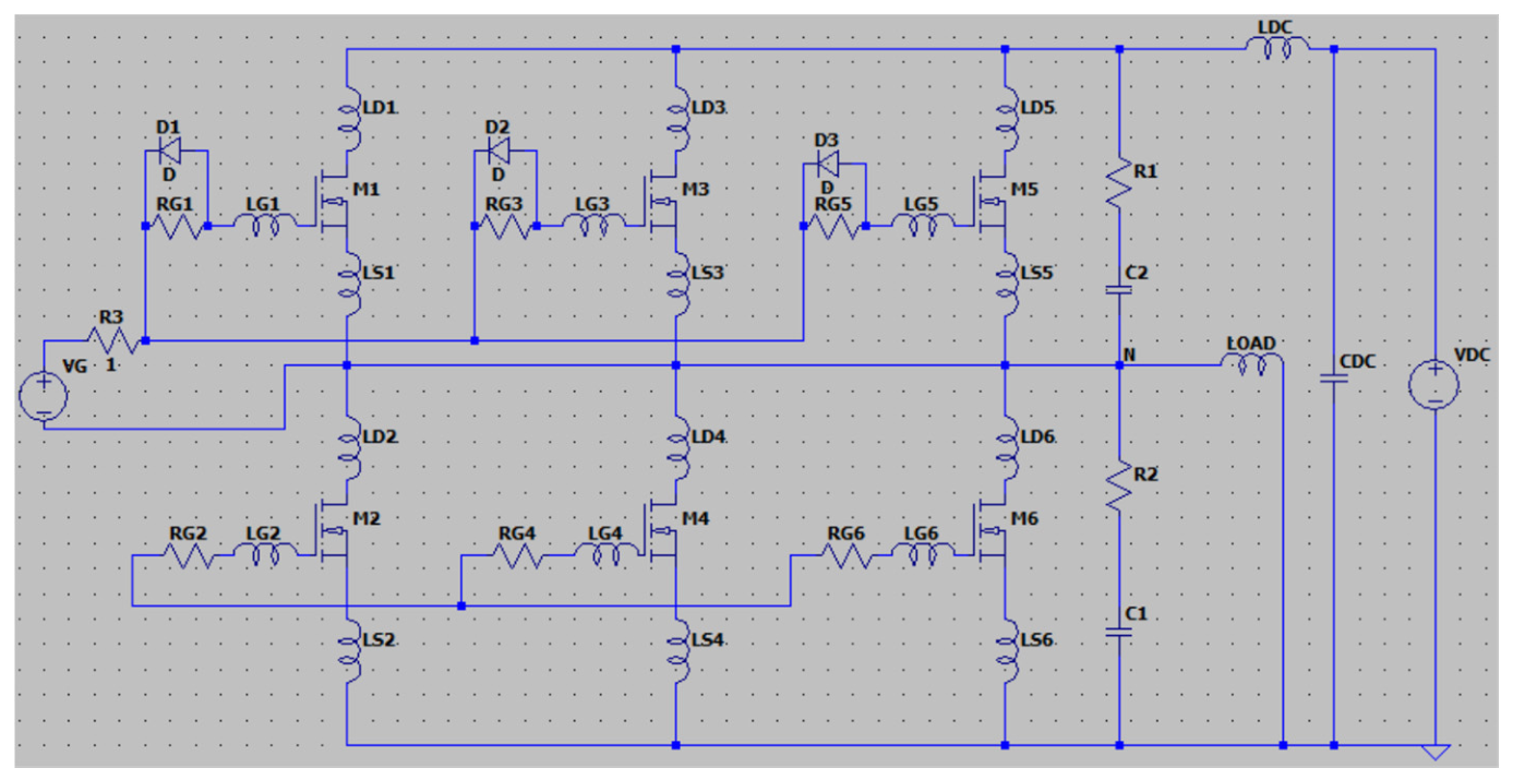
2. RC Snubber Circuits in Parallel MOSFET Configuration
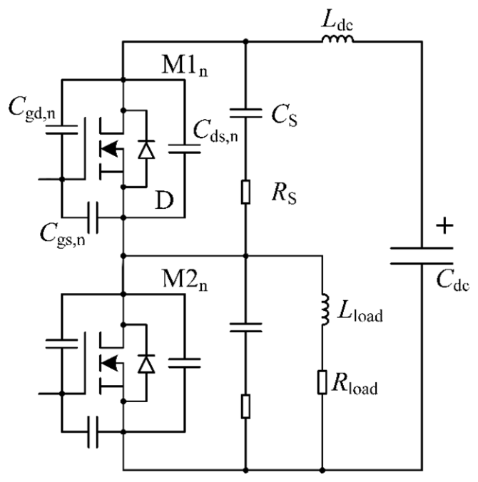
2.1. Simplified Analytical Model Development
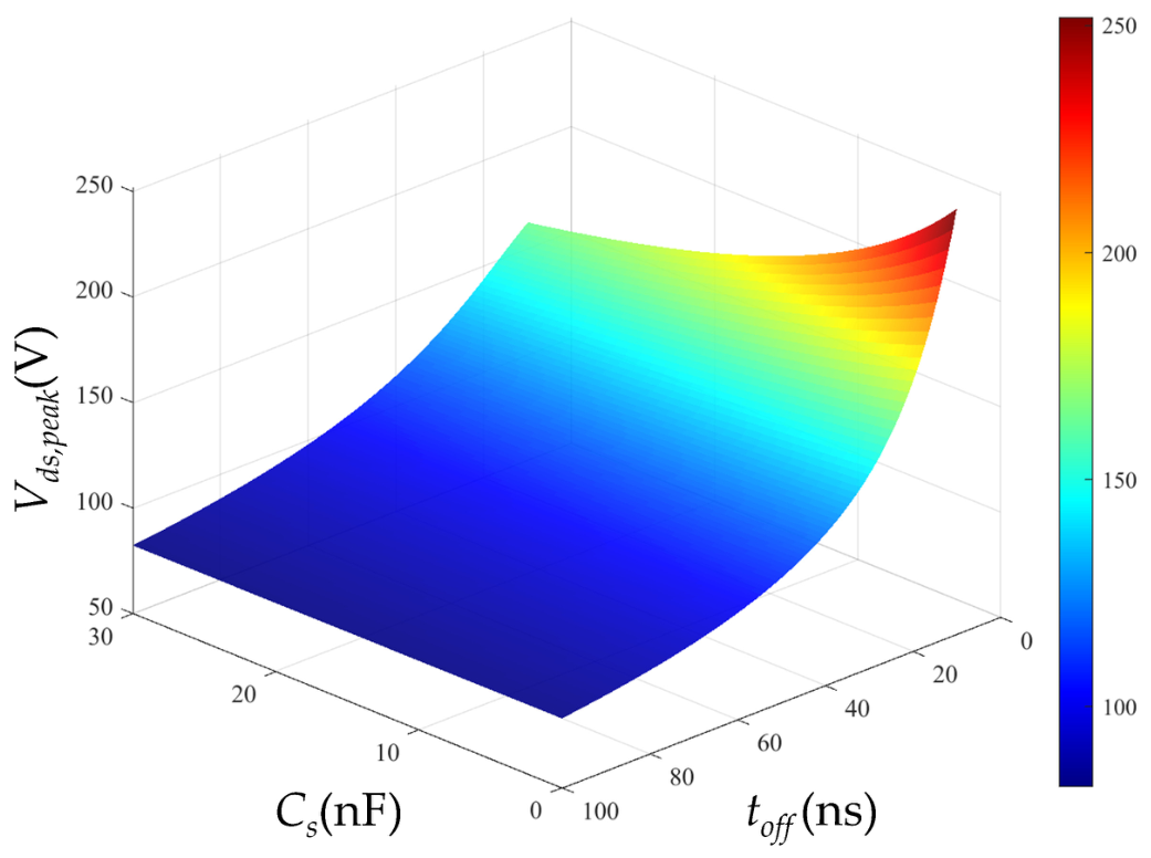
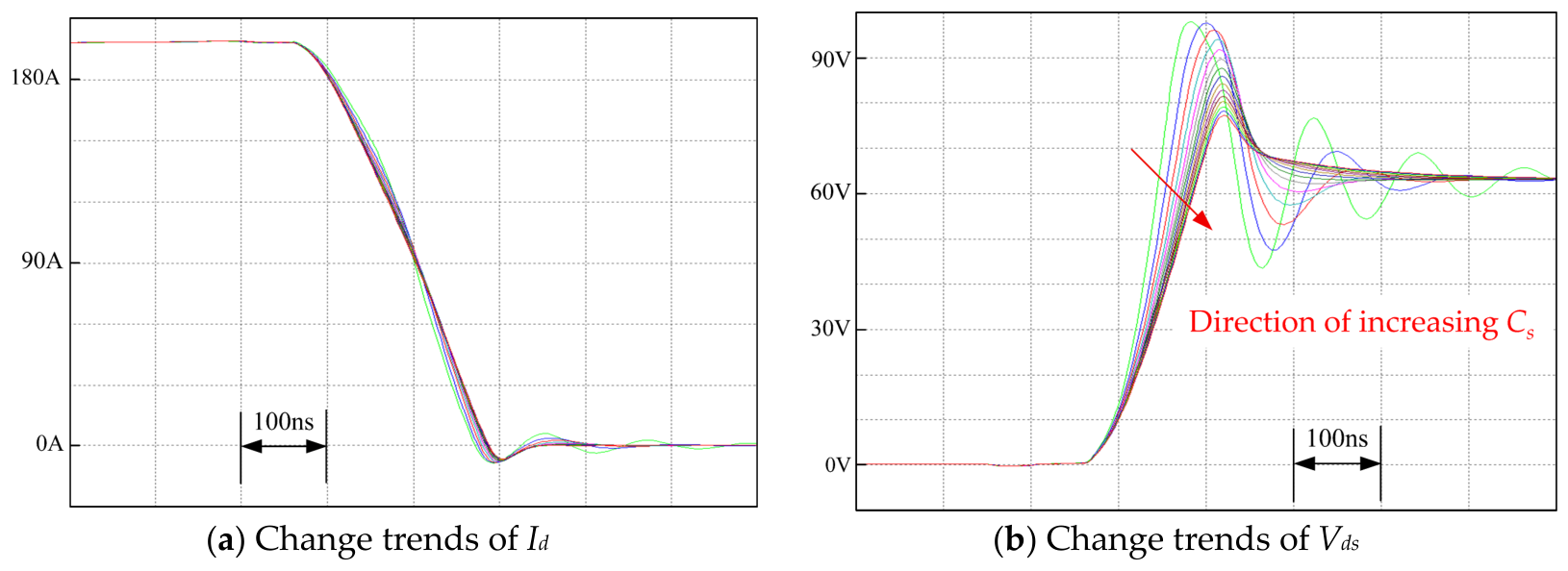
2.2. Analysis of Turn-Off Voltage Spikes
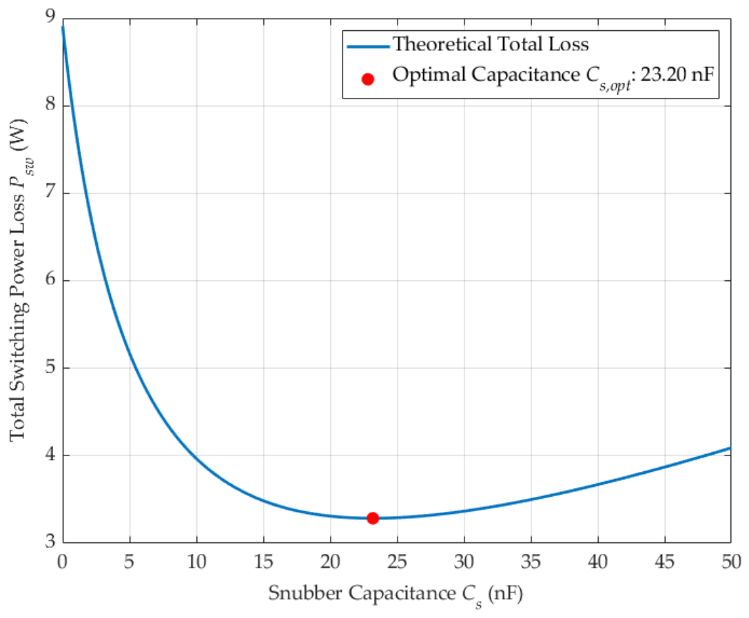
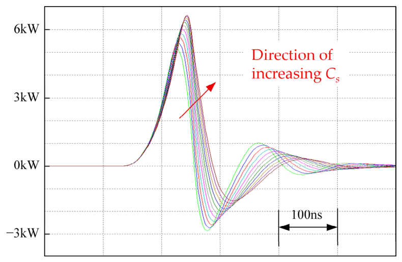
3. Total Turn-Off Loss Modeling of Paralleled MOSFET Circuits with an RC Snubber
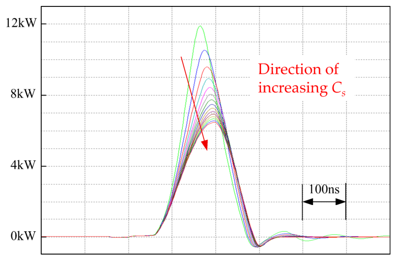
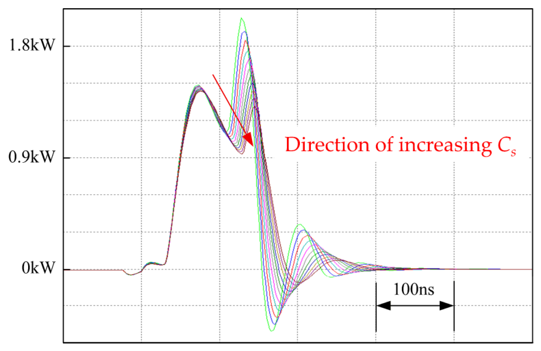
3.1. Comprehensive Turn-Off Loss Modeling with MOSFET, RC Snubber, and Bus Inductance Effects
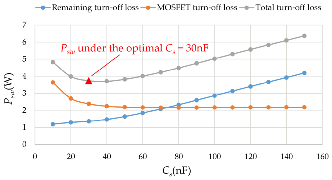
3.2. Simulation Validation
4. Experimental Verification
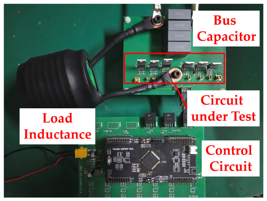
4.1. Experimental Platform
4.2. Measurement of Busbar Parasitic Inductance
4.3. The Effectiveness of RC Snubber Circuits in Suppressing Voltage Spikes
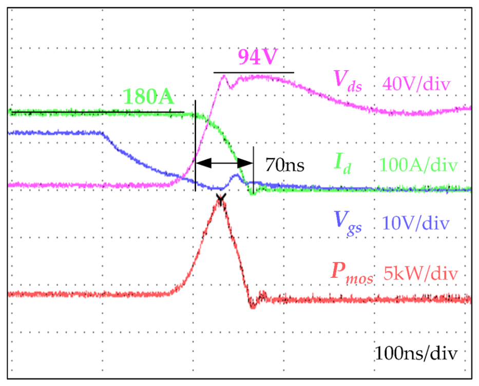
4.4. Measurement of Total Turn-Off Losses
5. Conclusions
Author Contributions
Funding
Data Availability Statement
Conflicts of Interest
References
- Kinyua, J.M.; Aoki, M. SiC MOSFET Switching Dynamics and Power Conversion Loss Characterization Under Parametric Variations. Energies 2025, 18, 6264. [Google Scholar] [CrossRef] [Scilit]
- Wu, Y.; He, N.; Yu, L.; Xu, D.; Igarashi, S.; Fujihira, T. Effectiveness analysis of SiC MOSFET switching oscillation damping. In Proceedings of the 2020 IEEE 9th International Power Electronics and Motion Control Conference (IPEMC2020-ECCE Asia), Nanjing, China, 29 November–2 December 2020; pp. 20–27. [Google Scholar] [CrossRef] [Scilit]
- Park, B.J.; Hwang, C.J.; Park, G.U.; Park, M.S.; Shim, D. Drain-Voltage Assessment-Based RC Snubber Design Approach for GaN HEMT Flyback Converters. Electronics 2026, 15, 271. [Google Scholar] [CrossRef] [Scilit]
- Liu, X.; Li, H.; Lin, J.; Song, C.; Zhang, H.; Xue, Y.; Zhang, H. Mitigation of Switching Ringing of GaN HEMT Based on RC Snubbers. Aerospace 2025, 12, 885. [Google Scholar] [CrossRef] [Scilit]
- Yu, J.; Shen, R.; Zhou, L.; Jia, Z.; Hao, Y. Investigation of a Low-Speed Commutation Voltage Shock Problem in Three-Level ANPC Inverter with Hybrid Modulation Mode. Machines 2023, 12, 27. [Google Scholar] [CrossRef] [Scilit]
- Parashar, S.; Rawat, S.; Kolli, N.; Kokkonda, R.K.; Bhattacharya, S. Comparative Performance Analysis of Medium Voltage 3L-ANPC and 3L-DNPC Pole Enabled by series-Connection of 10kV SiC MOSFETs and 10kV SiC JBS Diodes for Sine Triangle PWM Operation. In Proceedings of the 2025 IEEE Applied Power Electronics Conference and Exposition (APEC), Atlanta, GA, USA, 16–20 March 2025; pp. 1347–1354. [Google Scholar] [CrossRef] [Scilit]
- Heidari, R.; Adib, E.; Jeong, K.I.; Ahn, J.W. Soft-switched boost–cuk-type high step-up converter for grid-tied with half-bridge inverter. IEEE J. Emerg. Sel. Top. Power Electron. 2022, 11, 786–795. [Google Scholar] [CrossRef] [Scilit]
- Ma, K.; Shi, Y.; Su, J.; Lai, J.; Yu, X. A simplified method for calculating switching losses in power MOSFETs taking parasitic parameters into account. Trans. China Electrotech. Soc. 2021, 36, 591–599. [Google Scholar] [CrossRef]
- Shi, Z.; Wei, L.; He, J.; Li, G.; Song, C. Optimization of Snubber Circuit Parameters for AC–AC Chopper Converter. Electronics 2025, 14, 1733. [Google Scholar] [CrossRef] [Scilit]
- Bryant, B.M.; Lemmon, A.N.; DeBoi, B.T.; New, C.D.; Jimenez, S.J. Improved Methodology for Estimating Switching Losses of Wide-Bandgap Semiconductors Using Gaussian Curve Fitting. IEEE Trans. Power Electron. 2024, 39, 5590–5601. [Google Scholar] [CrossRef] [Scilit]
- Singh, V.K.; Tripathi, R.N. Paralleling of Gallium Nitride Power Semiconductor Devices: A Review and Future Perspectives. Electronics 2026, 15, 1607. [Google Scholar] [CrossRef] [Scilit]
- Morsy, A.S.; Enjeti, P.N. Comparison of active power decoupling methods for high-power-density single-phase inverters using wide-bandgap FETs for Google little box challenge. IEEE J. Emerg. Sel. Top. Power Electron. 2016, 4, 790–798. [Google Scholar] [CrossRef] [Scilit]
- McMurray, W. Optimum snubbers for power semiconductors. IEEE Trans. Ind. Appl. 1972, 8, 593–600. [Google Scholar] [CrossRef] [Scilit]
- Xu, M.; Yang, X.; Li, J. C-RC snubber optimization design for improving switching characteristics of SiC MOSFET. IEEE Trans. Power Electron. 2022, 37, 12005–12016. [Google Scholar] [CrossRef] [Scilit]
- Liu, B.; Li, W.; Meng, D.; Diao, L.; Ma, Y.; Qiu, T.; Diao, L. Low-stray inductance optimized design for power circuit of SiC-MOSFET-based inverter. IEEE Access 2020, 8, 20749–20758. [Google Scholar] [CrossRef] [Scilit]
- Yang, X.; Xu, M.; Li, Q.; Wang, Z.; He, M. Analytical method for RC snubber optimization design to eliminate switching oscillations of SiC MOSFET. IEEE Trans. Power Electron. 2021, 37, 4672–4684. [Google Scholar] [CrossRef] [Scilit]
- Sayed, H.; Zurfi, A.; Zhang, J. Investigation of the effects of load parasitic inductance on SiC MOSFETs switching performance. In Proceedings of the 2017 IEEE International Conference on Industrial Technology (ICIT), Toronto, ON, Canada, 22–25 March 2017; pp. 125–129. [Google Scholar] [CrossRef] [Scilit]



| Cs (nF) | MOSFET Turn-Off Loss (W) | Remaining Turn-Off Loss (W) | Psw (W) | Cs (nF) | MOSFET Turn-Off Loss (W) | Remaining Turn-Off Loss (W) | Psw (W) |
|---|---|---|---|---|---|---|---|
| 10 | 3.64 | 1.19 | 4.82 | 90 | 2.16 | 2.59 | 4.75 |
| 20 | 2.70 | 1.29 | 3.99 | 100 | 2.17 | 2.86 | 5.03 |
| 30 | 2.34 | 1.36 | 3.70 | 110 | 2.17 | 3.13 | 5.3 |
| 40 | 2.24 | 1.46 | 3.71 | 120 | 2.17 | 3.40 | 5.57 |
| 50 | 2.19 | 1.64 | 3.82 | 130 | 2.17 | 3.66 | 5.83 |
| 60 | 2.17 | 1.84 | 4.01 | 140 | 2.18 | 3.92 | 6.10 |
| 70 | 2.16 | 2.07 | 4.23 | 150 | 2.18 | 4.19 | 6.37 |
| 80 | 2.16 | 2.33 | 4.48 |
| Cs (nF) | MOSFET Turn-Off Loss (W) | Remaining Turn-Off Loss (W) | Psw (W) | Cs (nF) | MOSFET Turn-Off Loss (W) | Remaining Turn-Off Loss (W) | Psw (W) |
|---|---|---|---|---|---|---|---|
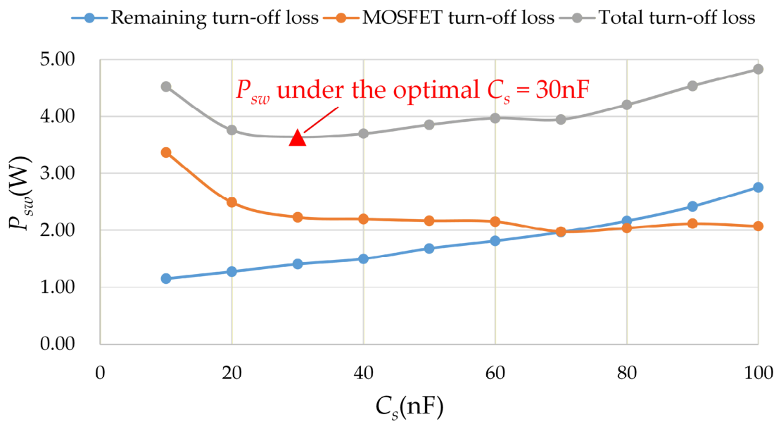
| 10 | 3.37 | 1.15 | 4.52 | 60 | 2.16 | 1.81 | 3.97 |
| 20 | 2.49 | 1.27 | 3.76 | 70 | 1.98 | 1.97 | 3.94 |
| 30 | 2.23 | 1.40 | 3.63 | 80 | 2.04 | 2.17 | 4.21 |
| 40 | 2.20 | 1.49 | 3.69 | 90 | 2.12 | 2.41 | 4.53 |
| 50 | 2.17 | 1.68 | 3.85 | 100 | 2.08 | 2.75 | 4.83 |
| Verification Method | Cs,opt (nF) | Psw,opt (W) |
|---|---|---|
| Theoretical calculation | 23.2 | 3.25 |
| Simulation | 30 | 3.70 |
| Experiment | 30 | 3.63 |
Disclaimer/Publisher’s Note: The statements, opinions and data contained in all publications are solely those of the individual author(s) and contributor(s) and not of MDPI and/or the editor(s). MDPI and/or the editor(s) disclaim responsibility for any injury to people or property resulting from any ideas, methods, instructions or products referred to in the content. |
© 2026 by the authors. Licensee MDPI, Basel, Switzerland. This article is an open access article distributed under the terms and conditions of the Creative Commons Attribution (CC BY) license.
Share and Cite
Xu, Y.; Wu, Z.; Hua, W. A Method for Optimizing Turn-Off Losses Design in Parallel MOSFETs Inverter with RC Snubber Circuits. Energies 2026, 19, 4315. https://doi.org/10.3390/en19184315
Xu Y, Wu Z, Hua W. A Method for Optimizing Turn-Off Losses Design in Parallel MOSFETs Inverter with RC Snubber Circuits. Energies. 2026; 19(18):4315. https://doi.org/10.3390/en19184315
Chicago/Turabian StyleXu, Yang, Zheng Wu, and Wei Hua. 2026. "A Method for Optimizing Turn-Off Losses Design in Parallel MOSFETs Inverter with RC Snubber Circuits" Energies 19, no. 18: 4315. https://doi.org/10.3390/en19184315
APA StyleXu, Y., Wu, Z., & Hua, W. (2026). A Method for Optimizing Turn-Off Losses Design in Parallel MOSFETs Inverter with RC Snubber Circuits. Energies, 19(18), 4315. https://doi.org/10.3390/en19184315