2.1. DC Bus Voltage Instability in Standalone PV Systems
In standalone PV-based grid-forming systems, the inverter autonomously establishes the grid voltage and frequency; therefore, the DC bus must continuously provide a stable DC voltage to the inverter even under PV power fluctuations and abrupt load changes. In practical operation, however, a power imbalance between the generated power and load demand repeatedly occurs over short timescales, which can cause instantaneous DC bus voltage drops or transient over-voltages.
The primary cause of DC bus voltage instability is the mismatch between the source power
and load power
. In particular, when the load increases sharply, the PV flyback converter may not be able to supply the required power immediately owing to its dynamic and control bandwidth limitations, thereby inducing a DC bus voltage drop. This mismatch can be defined as a deficit power
, and is given as
Such a deficit power can directly deteriorate the voltage and frequency quality generated by the inverter in grid-forming systems, leading to degraded power quality and unstable system operation.
2.2. Features of Supercapacitors
Supercapacitors provide a high power density owing to their low equivalent series resistance and very fast charge–discharge response, and they exhibit minimal performance degradation even after hundreds of thousands of cycles, making them well suited for transient power compensation [
14,
15,
16]. They can rapidly supply or absorb energy when the DC bus voltage deviates from its reference value, thereby reducing the burden on the grid-forming inverter for maintaining the system voltage and frequency.
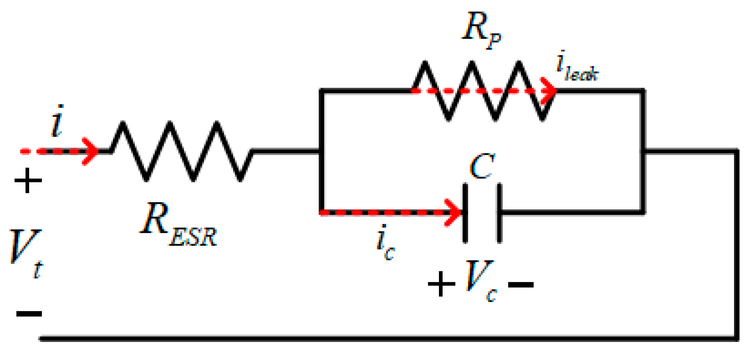
The electrical characteristics of a supercapacitor are commonly modeled using equivalent series resistance (ESR) [
16], parallel leakage resistance
, and capacitance C (
Figure 1). Accordingly, the equivalent impedance in the frequency domain can be approximated as
Although a low ESR is advantageous for transient power compensation, directly connecting a supercapacitor to a DC bus can induce a large current inrush [
14,
16]. The initial inrush current is determined by Equation (3). A smaller
results in a higher current, imposing electrical and thermal stresses on the switching devices.
where
denotes the DC bus voltage. Therefore, in this study, the supercapacitor was not directly connected to the DC bus. Instead, a bidirectional flyback converter with Constant Current (CC)–Constant Voltage (CV) charging and a soft-start scheme were employed to limit the initial current. Beyond current limiting, the bidirectional converter provides essential voltage decoupling between the wide operating range of the supercapacitor and the stable DC bus, ensuring precisely controlled power flow during ride-through operations [
17,
18].
While more complex models considering parasitic inductive effects and frequency-dependent ESR are available for high-frequency transient analysis, the classic series $RC$ model is adopted in this study. This simplification is justified as the primary objective is to evaluate the low-frequency energy balance and the total ride-through duration. For capacitance sizing based on deficit power, this model provides sufficient accuracy while maintaining analytical clarity for engineering applications.
2.3. Ride-Through Control Using Supercapacitors
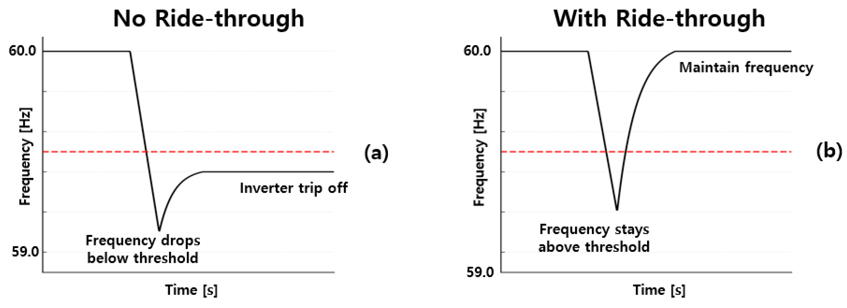
Ride-through refers to the capability of a system to maintain continuous operation for a certain period without immediate shutdown [
5,
6,
7,
8], even under grid disturbances or external perturbations (
Figure 2). In this study, it was applied to the DC bus voltage drop caused by abrupt load changes in a standalone PV-based grid-forming system [
6,
10,
11]. The objective is to compensate for the deficit power
induced by load transients through supercapacitor discharge, thereby maintaining the DC bus voltage within an allowable range and ensuring stable inverter operation.
However, ride-through compensation performance strongly depends on the capacitance of the supercapacitor. If the capacitance is undersized, the available stored energy may be insufficient to meet the target compensation duration, leading to an excessive DC bus voltage drop and potentially triggering protective actions or a shutdown. Conversely, oversizing can improve transient support but unnecessarily increases the system cost and volume [
5,
7,
9,
12], reducing the overall practicality. Therefore, a quantitative sizing procedure that determines the minimum required capacitance based on the magnitude of the load disturbance and the allowable voltage drop is essential.
The overview and operating logic of ride-through control are as follows: The DC bus voltage is monitored in real time, and a ride-through action is triggered when deviates from the allowable range around the reference voltage or when a voltage drop is detected. If the supercapacitor voltage lies within the prescribed operating range, a compensation flag is enabled, and a discharge command is generated to inject power into the DC bus through the bidirectional converter. During discharge, the ride-through operation is terminated, and the system returns to the standby state once the DC bus voltage recovers and re-enters the normal range, or once the supercapacitor voltage reaches its minimum allowable value.
Under an abrupt load change, the deficit power required at the DC bus is given by Equation (1). When
, insufficient source power is available, and the supercapacitor must compensate for this deficit by discharging. Assuming that the deficit power is compensated as a constant power, the energy required by the DC bus over the compensation interval
is
The ideal stored energy that a supercapacitor (
) can provide for power compensation is limited by the initial and final voltages, and can be expressed as
where
is the supercapacitor capacitance,
is the discharge-start voltage, and
is the minimum allowable voltage to prevent overdischarge. In practical compensation, the energy delivered to the DC bus is reduced owing to the conversion efficiency
and ESR-related losses; thus, the effective energy
can be expressed as follows:
To ensure the reproducibility of the predicted effective energy () and ride-through duration (), the exact operational parameters utilized in the theoretical calculations are specified as follows: the nominal DC-bus voltage = 50 V, the minimum allowable voltage drop = 45 V, the measured converter efficiency = 92.4%, and the equivalent series resistance = 0.12 Ω. Using these static design values, any independent researcher can identically reproduce the analytical results yielded by Equations (6) and (7).
Here, “” represents the power conversion efficiency of the bidirectional DC-DC converter, accounting for the losses during the energy transfer between the supercapacitor and the DC bus.
Therefore, assuming that the deficit power is compensated for as a constant power, the ride-through sustained time achieved using the supercapacitor is derived as
Given a target ride-through time
, the minimum required supercapacitor capacitance based on the ideal model is as follows:
In a practical design, it is advisable to apply a safety margin by accounting for variations in efficiency, ESR, sensing errors, and uncertainties associated with disturbances. Overall, the equations derived in this section provide a quantitative design basis for determining a supercapacitor capacitance that satisfies the required compensation duration.
2.4. Operating Scenarios and Performance Evaluation Metrics
The deficit-power-based compensation formulation and ride-through time derivation presented in
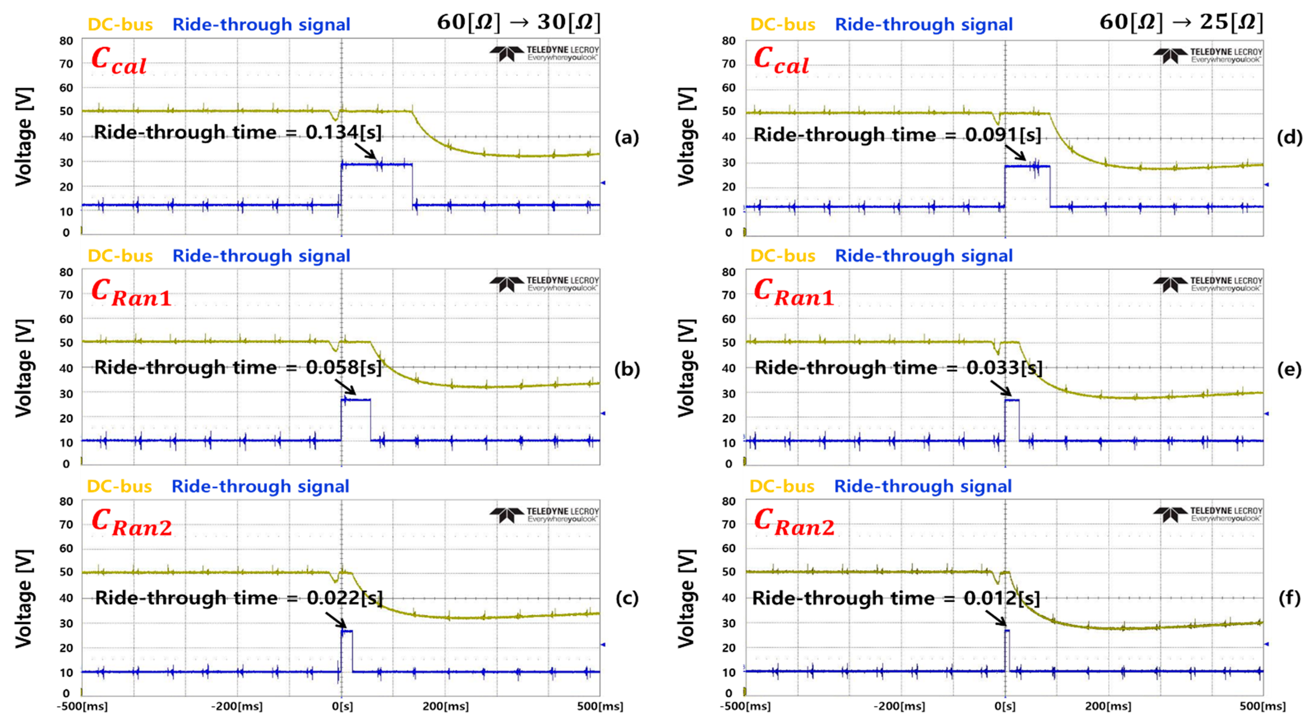
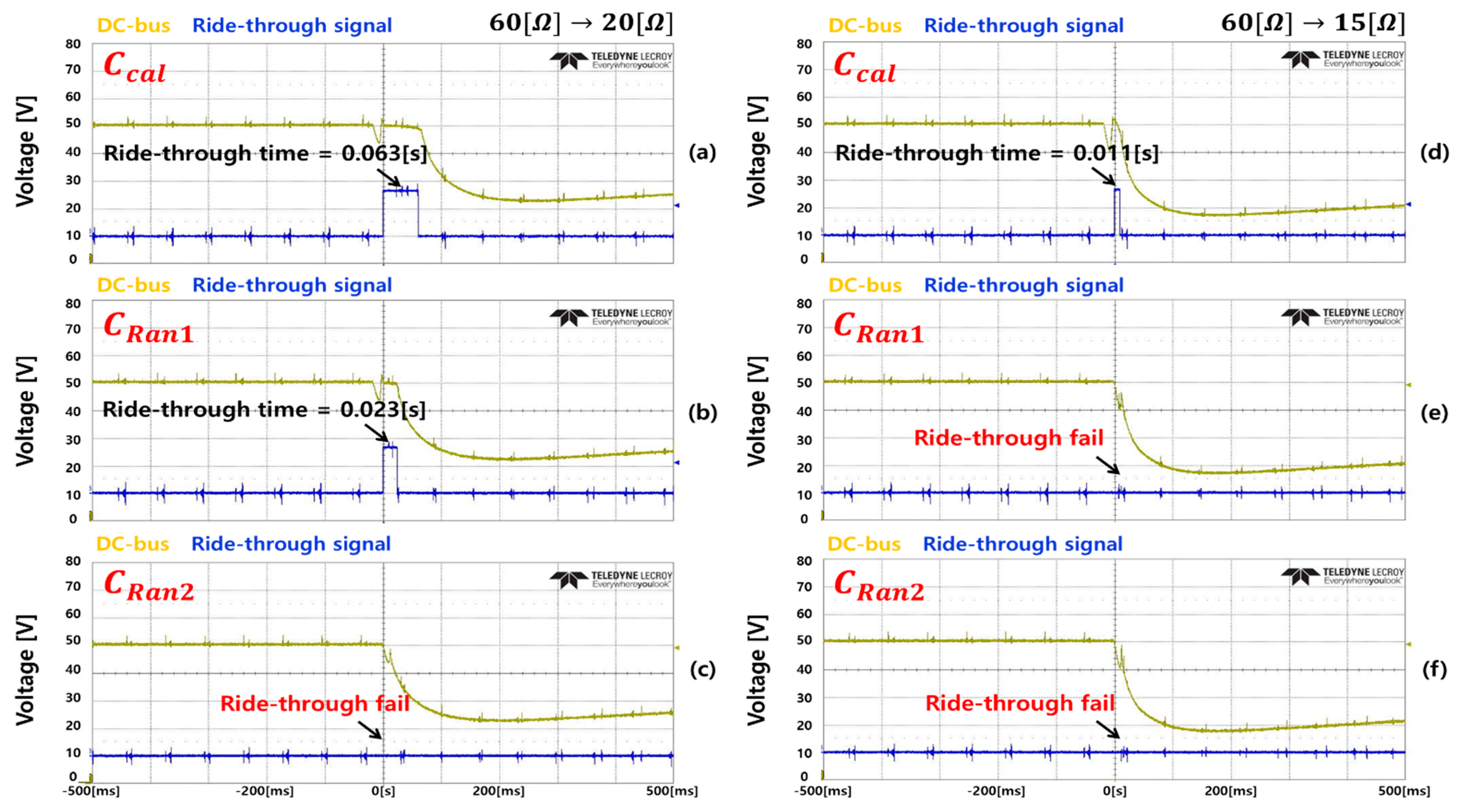
Section 2.3 were validated through PSIM simulation. In both the simulation and experiments, abrupt operating conditions frequently encountered in standalone PV systems, such as step changes in load resistance, were considered, and supercapacitor discharge compensation was applied based on the corresponding deficit power
during the transient interval. The results showed that when the supercapacitor capacitance was selected according to the proposed design equations, the DC bus voltage drop was confined within the specified allowable range, and the transient response exhibited a stable recovery to the normal operating region. In addition, the ride-through duration during the compensation interval showed an overall agreement between the analytically predicted time and the time observed in the simulation, confirming that the proposed quantitative sizing procedure is effective in determining the capacitance required to meet the target compensation time.
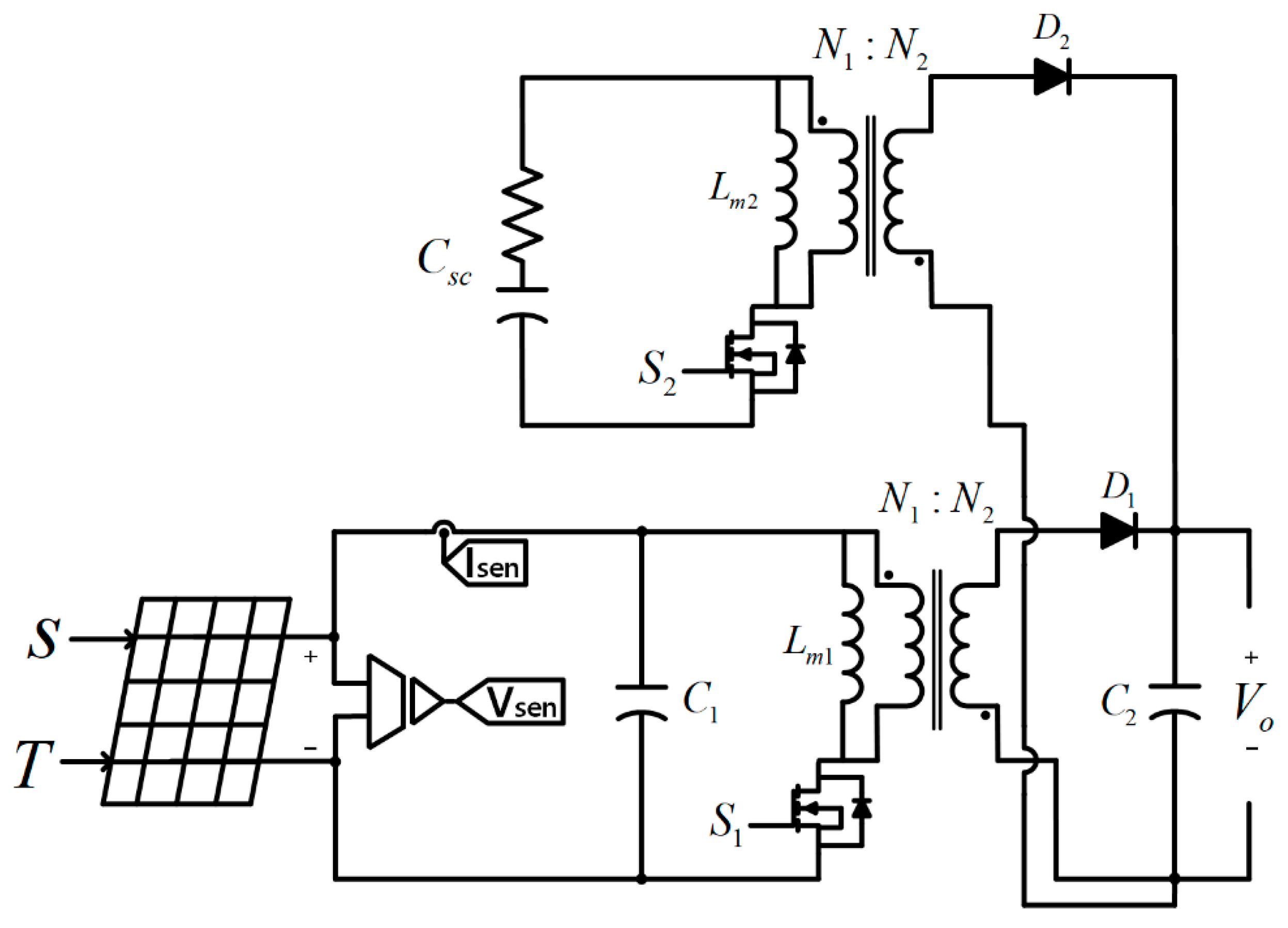
Figure 3 illustrates the simplified equivalent circuit used for the analytical derivation. In this model,
denotes the supercapacitor voltage, while
and
represent the equivalent inductance and diode for energy transfer, respectively.
indicates the DC-bus capacitance, and
represents the target DC-bus voltage (50 V) maintained during the ride-through operation. This idealized configuration focuses on the fundamental power flow from the supercapacitor to the load, providing a basis for calculating the required capacitance.
To verify the validity of the deficit power estimation for ride-through control, simulations were conducted using the circuit shown in
Figure 3; the parameters are listed in
Table 1.
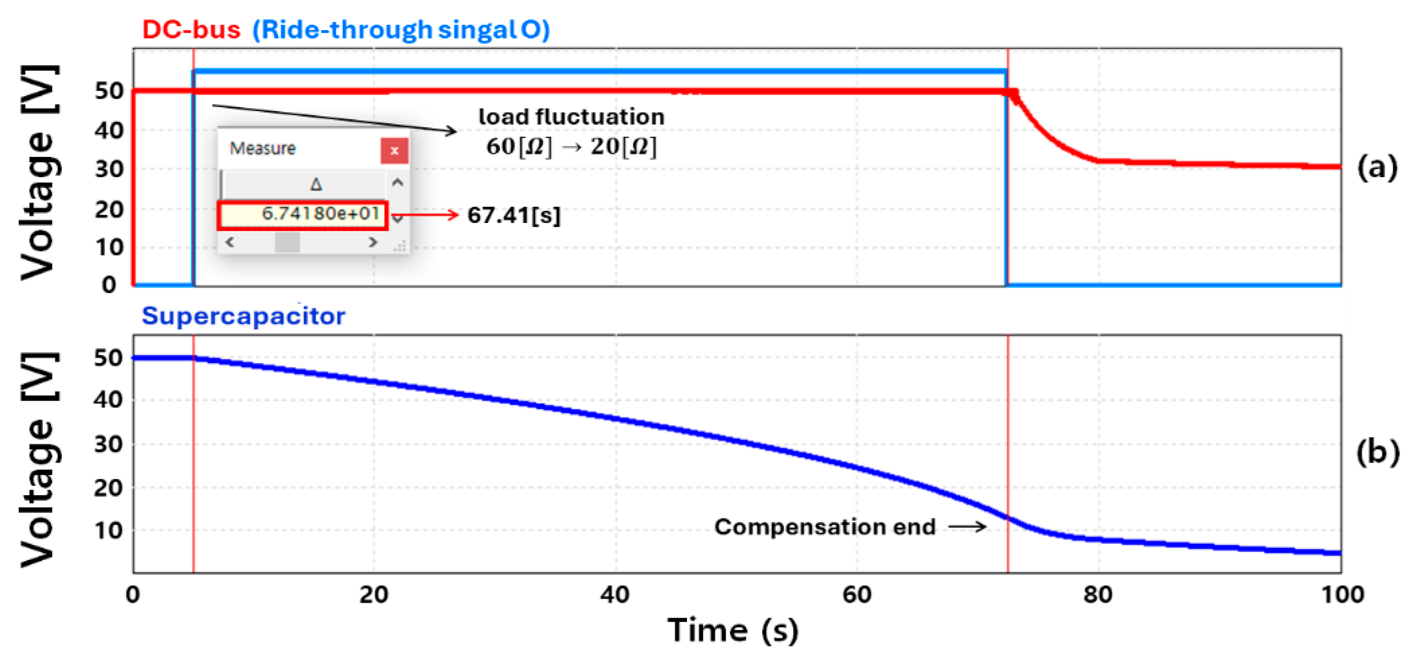
Figure 4 presents the detailed transient responses during the ride-through operation. Specifically,
Figure 4a shows the time-domain responses of the DC bus voltage and the ride-through compensation signal, while
Figure 4b presents the voltage and current waveforms of the supercapacitor. When the load mutation occurs, the DC bus voltage initially drops, but the proposed control strategy immediately triggers the bidirectional converter. The voltage recovery dynamics exhibit a rapid stabilization back to the target operating range within a few milliseconds, demonstrating that the PI controller effectively regulates the power flow from the supercapacitor.
In the PSIM simulation performed with the design capacity of 4.7 F, the compensation hold time calculated from the ideal mathematical model is (67.41 s), and the observed simulation hold time is (67.50 s). The discrepancy between the two results is (0.09 s), which is primarily attributed to the inherent limitation of the discrete Perturb and Observe (P&O) Maximum Power Point Tracking (MPPT) method [
13,
19]. In this discrete control scheme, the PV output voltage continuously oscillates around the Maximum Power Point, meaning that the
cannot be maintained as a perfectly constant value, leading to the minor timing deviation.
In practical standalone PV systems, large-capacity supercapacitors on the order of a few to several tens of farads are required to achieve such long-term ride-through capability. However, this study primarily focused on validating the fundamental operating principle of the ride-through control loop and its transient response characteristics at the DC bus side. Therefore, for feasible laboratory-scale hardware verification, the capacitance was intentionally scaled down to (4700 µF) while keeping the underlying control structure and voltage variation mechanism identical. It should be noted as a boundary condition that this laboratory-scale setup was utilized to verify the mathematical validity of the capacity sizing method and the dynamic performance of the controller under scaled conditions, rather than replicating the longhold-time energy capacity or the complex electrochemical behavior inherent to full-scale supercapacitor modules.
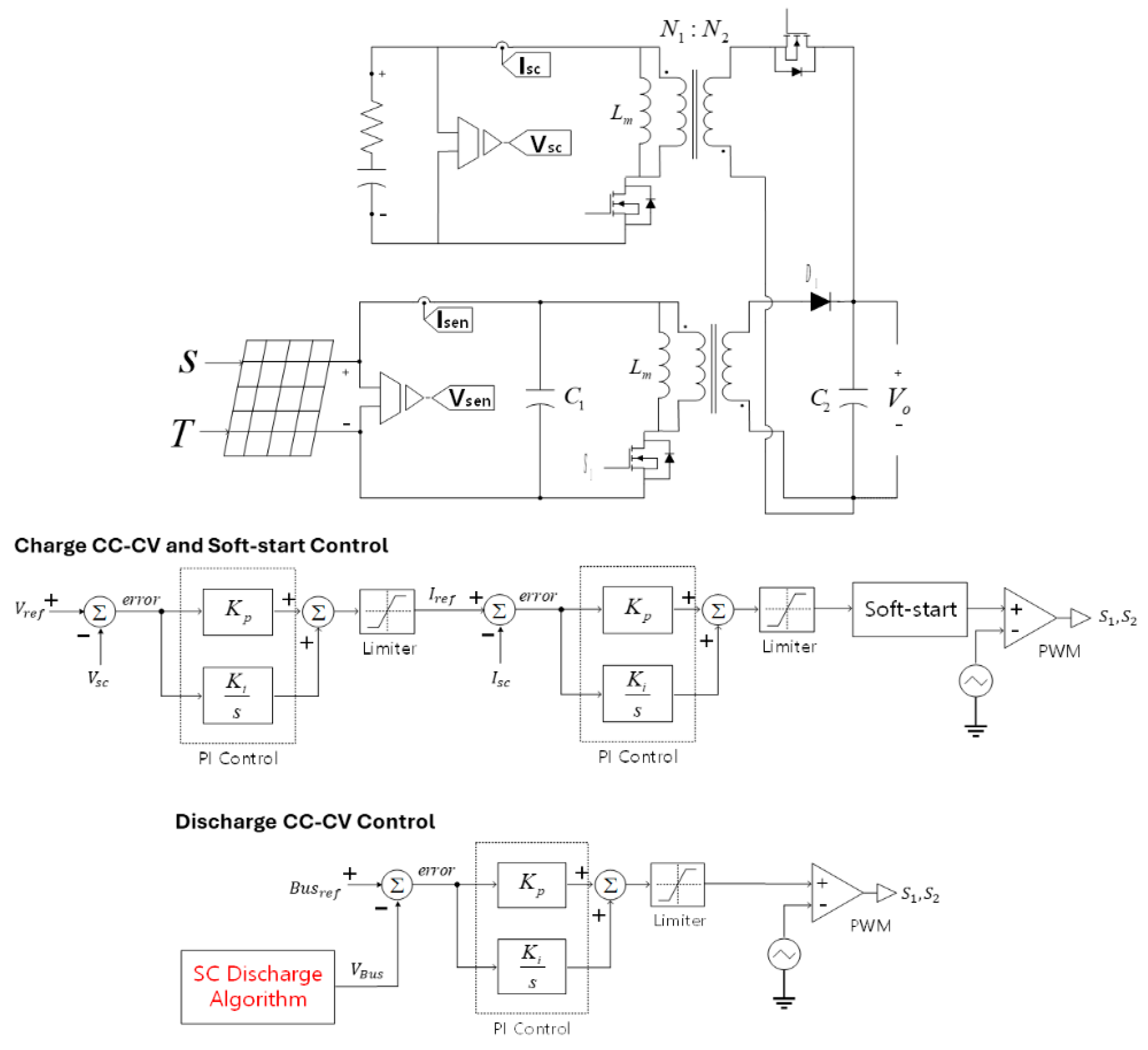
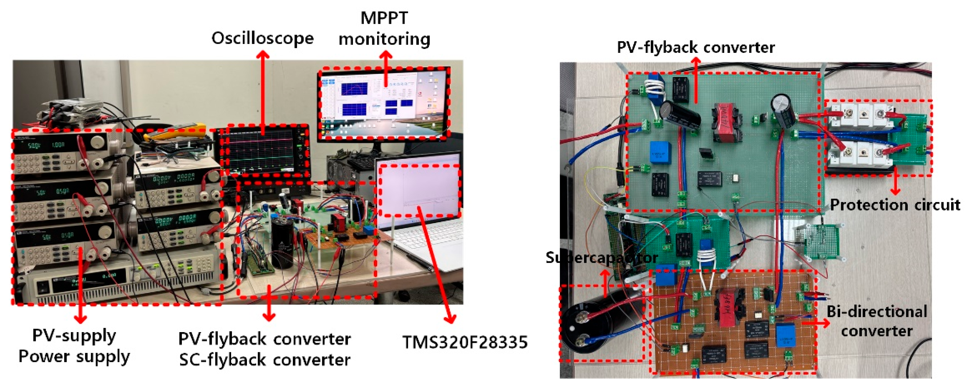
This section describes the hardware setup and operating scenarios used to experimentally validate sizing of the supercapacitor capacitance based on the deficit power. The experimental system consisted of a flyback converter driven by a PV panel as the input source and a bidirectional flyback converter that charged and discharged the supercapacitor [
14,
20]. The system operates in two modes: (i) the charging mode, which prepares the supercapacitor to a target voltage using CC–CV control with a soft start, and (ii) the discharging (ride-through) mode, which compensates for the deficit power caused by abrupt load changes (
Figure 5) [
14,
17,
18].
As illustrated in the detailed control structure (
Figure 5), the ride-through operation is governed by a digital PI controller implemented on a TMS320F28335 DSP (Texas Instruments, Dallas, TX, USA). To ensure both stability and a rapid dynamic response during transients, the control system employs a dual-loop configuration or a direct voltage regulation loop with high-speed execution at a sampling frequency of 20 kHz. The proportional and integral gains for the DC-bus voltage regulation were designed based on the bandwidth requirements and fine-tuned to
= 0.1 and
= 8.0. Furthermore, a slew-rate limit (
= 0.10) was applied to the duty cycle command to mitigate transient overshoots while ensuring the controller reacts within a few milliseconds. This identical control architecture and set of gains were utilized in both the PSIM simulations and hardware experiments to maintain consistency in performance validation.
The proposed ride-through control strategy is executed through a systematic state-machine logic consisting of ARM, HOLD, and SUPPORT modes to ensure reliable operation. In the ARM mode, the system waits until the DC-bus voltage stabilizes above a predefined arming threshold (49.0 V) for a specific duration (50 ms). Once armed, the system enters the HOLD mode, where it continuously monitors the bus voltage without triggering the converter. The transition to the SUPPORT (discharging) mode is initiated only when a significant voltage sag is detected—specifically, when the filtered bus voltage drops below a relative threshold (1.0 V drop) or an absolute limit (49.0 V) for at least 30 consecutive samples (1.5 ms). This multi-stage triggering logic prevents unintended activations caused by transient noise and ensures that the supercapacitor power is injected precisely when the ride-through capability is required. The compensation continues until the bus voltage recovers or the supercapacitor reaches its lower voltage limit, at which point the system safely resets to the standby state.
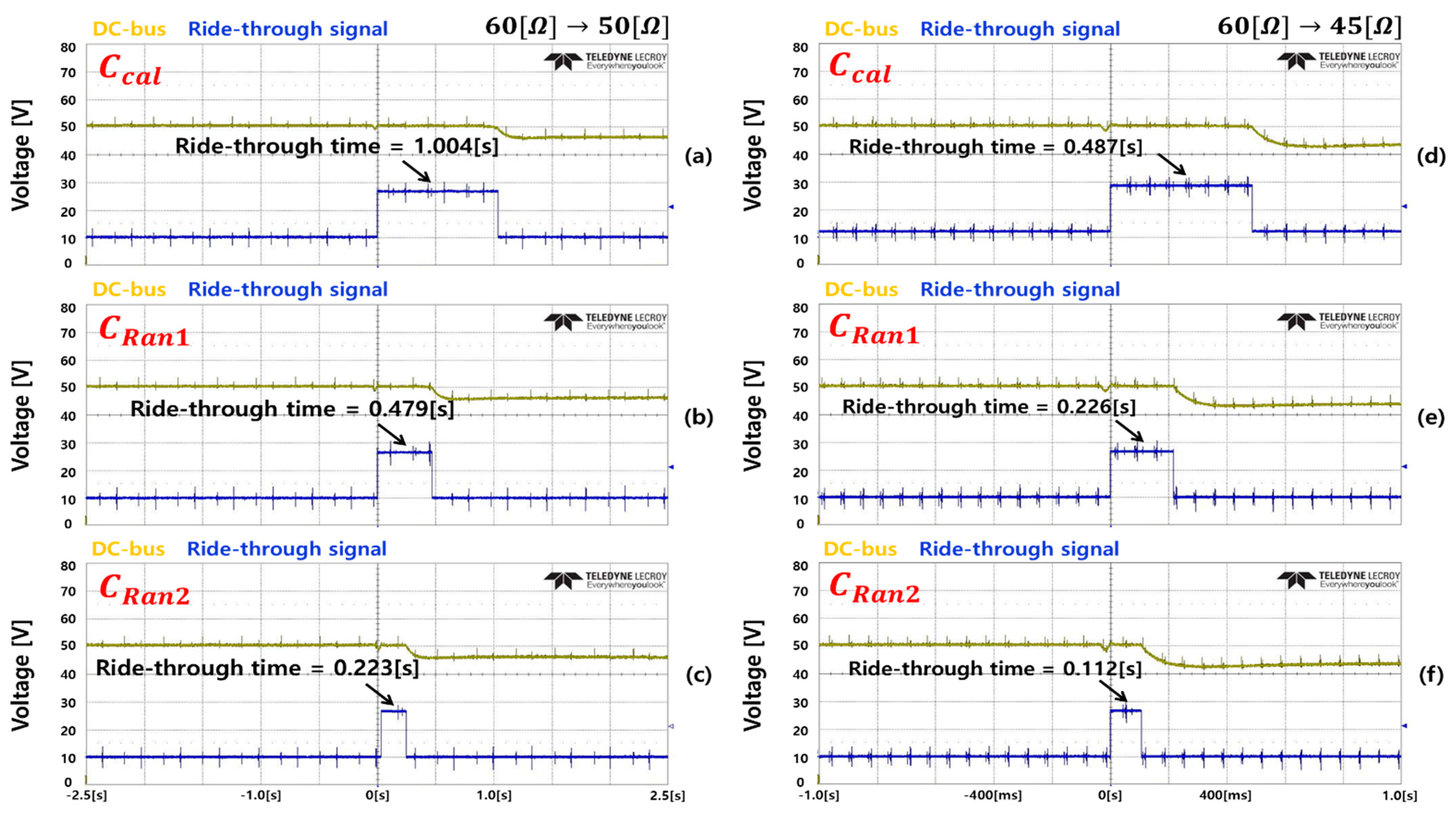
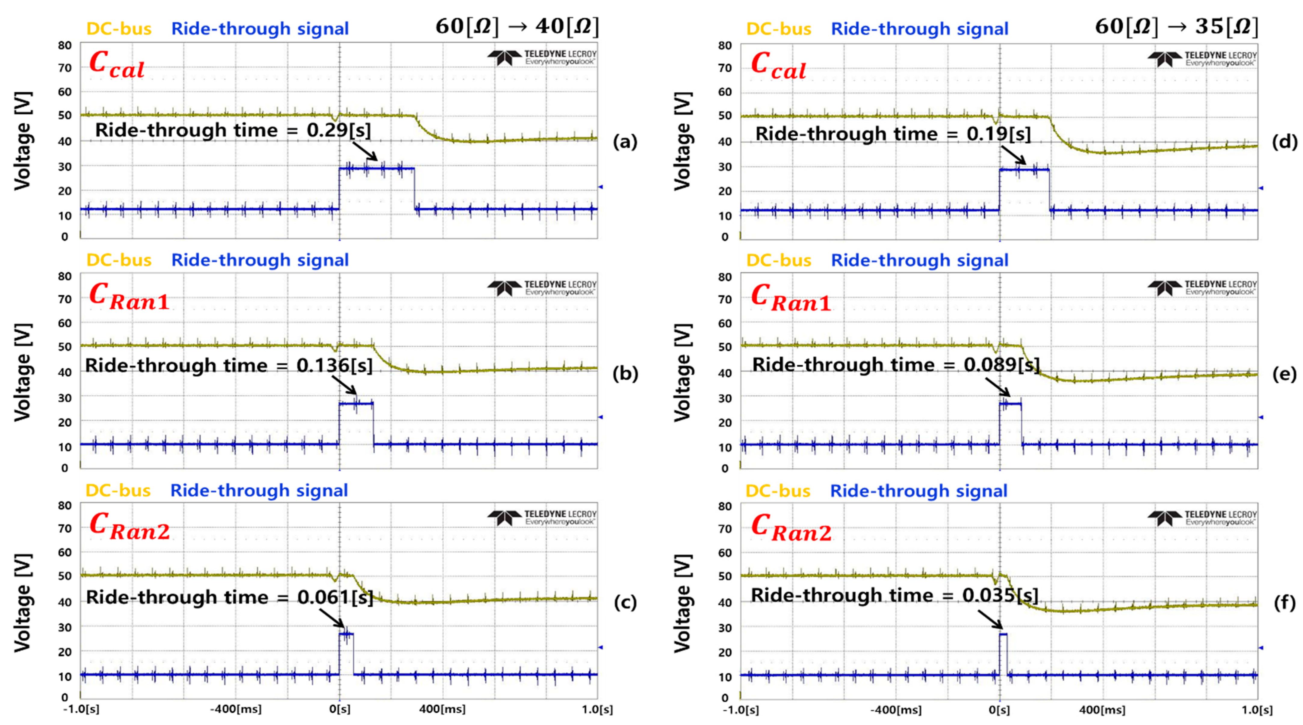
The experimental procedure was as follows. The supercapacitor is first charged within the prescribed voltage window (–) and the system then enters a standby state in which the DC bus voltage is continuously monitored. At a specified time, the load was varied in a stepwise manner (e.g., by reducing the load resistance) to intentionally induce a DC bus voltage drop, and the compensation power level was determined based on the resulting deficit power . When a voltage drop is detected, the system transitions to discharging mode and injects power into the DC bus through the bidirectional converter. The compensation is terminated when the supercapacitor voltage reaches or when the DC bus voltage recovers to the normal operating range. The experimental validation focuses on compliance with the allowable voltage-drop criterion and the reproducibility of the ride-through duration to assess the appropriateness of capacitance sizing.
Figure 3 presents the simplified circuit diagram used for the analytical derivation and simulation of the required capacitance sizing. For the actual hardware implementation, a bidirectional flyback converter topology was employed, as detailed in the control structure of
Figure 5.