Article

Input Power Quality Enhancement in Controlled Single-Phase AC to DC Converter

by
Naveed Ashraf
*,
Ghulam Abbas
and
Tanveer Yazdan
Department of Electrical Engineering, The University of Lahore, Lahore 54000, Pakistan
*
Author to whom correspondence should be addressed.
Energies 2025, 18(7), 1674; https://doi.org/10.3390/en18071674
Submission received: 27 February 2025 / Revised: 24 March 2025 / Accepted: 26 March 2025 / Published: 27 March 2025

Abstract

:
Voltage-controlled AC to DC converters govern the load voltage as per requirement. They may be employed in numerous applications, including battery-charging systems, light dimming, and industrial speed drive systems. The voltage regulation is based on the delay angle control of the thyristors, which has a simple gate control mechanism. Still, their input currents are highly distorted due to the generation of low-order harmonics. Also, their output voltage can only be regulated in step-down mode. The total harmonic distortion (THD) of the input current depends on the relative value of the fundamental frequency components to their non-fundamental component. The power factor (PF) also depends on these values, as well as the phase displacement angle, which is controlled by the firing delay. The improvement in THD and PF can be enhanced by maintaining the sinusoidal characteristics of the input current as much as possible. The use of an AC filter may enhance these characteristics, but filtering the low-order harmonics is a big challenge. This research suggests a novel control and circuit of a single-phase rectifier that may ensure the sinusoidal characteristics of the input current with a dual polarity-controlled output voltage. Thus, it improves the THD and PF for any polarity of the output DC voltage. A practical test circuit is built for the validation of the analytical and computer simulation results.

1. Introduction

Power quality improvement, specifically for input current, is a key consideration in the field of power electronics converters [1,2,3]. Its assessment is based on certain performance parameters like power factor (PF), the harmonic factor of any specific frequency component (HFn), and total harmonics distortion (THD) [4]. A reduction in harmonics and improvements in the input power factor ensure the maximum transfer of the useful (active) power from the source side towards the load. It also reduces the demand for the reactive power that is caused by the harmonics. Input current with characteristics close to sinusoidal behavior has an improved power factor [5]. This is because the total power factor is the product of the displacement and distortion power factors. The first factor is directly related to the load or impedance angle. This is due to the lead or lag nature of the load current concerning the input source voltage. The displacement angle caused by the load’s nature can be compensated for inherently by the presence of a DC link capacitor at the output stage. However, the displacement angle introduced by the delay angle of the thyristor is very challenging and cannot be tackled easily. The second component of the total power factor is degraded due to the presence of harmonics components. An improvement in the harmonics profile can be achieved by employing harmonics suppression filters, effective control techniques, or circuits.
Variable DC power supplies are widely employed in computers, power servers of computer networking [6], LED driving systems [7,8], charging mechanisms for electronic devices, electric vehicles, and DC microgrids [9,10,11,12]. In LED lighting applications, unidirectional rectifiers are employed with a low-output ripple and high power factor and lifetime. Electronic devices, including cell phones, require low-capacity batteries that are normally based on lithium-ion technology, where the power density requirement is high. The power flow for electric vehicle battery bank charging systems may be unidirectional or bidirectional. In many industrial applications, it is preferable to reduce the harmonic components in the AC input current to maximize the transfer of useful (active) power from the utility grid [13]. This is because the transfer of active power from the utility grid to the load only depends on the current component having a frequency equal to the source voltage. The other frequency components are the main source of harmonic distortion and reactive power [14,15,16].
The distortion in the output voltage and input current in the voltage-controlled single-phase rectifier circuits is inversely related, which means an improvement in the load ripple factor degrades the sinusoidal behavior of the line current. A two-stage converter is a traditional way to lower the harmonic distortions of both sides. The front-ended circuit is reserved for the reduction of harmonics in the source current, while the second circuit is responsible for the improvement in the output ripple factor. Overall volume, cost, circuit, and control complications are the main concerns with such a circuit approach [17,18]. On the other hand, power conversion in a single stage can reduce the size, lower the overall volume, and increase the efficiency.
Conventional voltage regulation techniques such as phase angle control, buck, boost, buck–boost, cuck, SEPIC, and zeta can also govern load voltage as per requirement. Boost topology is simple to use, and the input current has continuous features, but its output voltage is always greater than that of the source side. An additional voltage buck stage is mandatory to lower the output voltage. The reduction in output voltage with a direct approach leads to the discontinuity of the input current, which becomes a big source of harmonic distortion. Normally, harmonic suppression filters tackle this problem by operating solid-state switching devices with high switching frequencies. The basic role of this selection of high switching frequencies is to lower the component size and to shift the harmonics at high frequencies where they can be easily filtered. However, such hard-switching topologies are the main source of electromagnetic interference and may have complex solutions [19]. Passive and active power filters may enhance the improvement in power quality in the case of voltage-unbalancing situations in the grid or distortion created by the integration of non-linear devices in the power system [20,21,22].
The present manuscript introduces a new DC voltage control approach that ensures the sinusoidal characteristics of the input current. For the voltage step-up method, the suggested converter operates in boost mode, which ensures the sinusoidal nature of the input current. For the voltage step-down process, it converts AC power to DC power by maintaining the number of positive and negative output half cycles. This variation in the output DC voltage is obtained with the proper arrangement of output pulses, which are achieved by converting the half cycles of the source voltage in their inverting or non-inverting form at the output. In this case, the instantaneous input current remains continuous, with a fixed peak value. The characteristics of the source current remain sinusoidal, ensuring a low distortion factor and improved power factor.
This paper includes different sections to explore the operation and analysis of the recommended approach. The introduction of the various AC to DC topologies, along with their application, merits or demerits, and research problems, are discussed in Section 1. Section 2 deals with the operating principles or modes of the proposed topology. The effectiveness of the work undertaken is compared with some other circuits producing similar outputs in Section 3. The validation of the work undertaken is tested with the computer-based results and test bench results in Section 4. Conclusions are determined in Section 5.

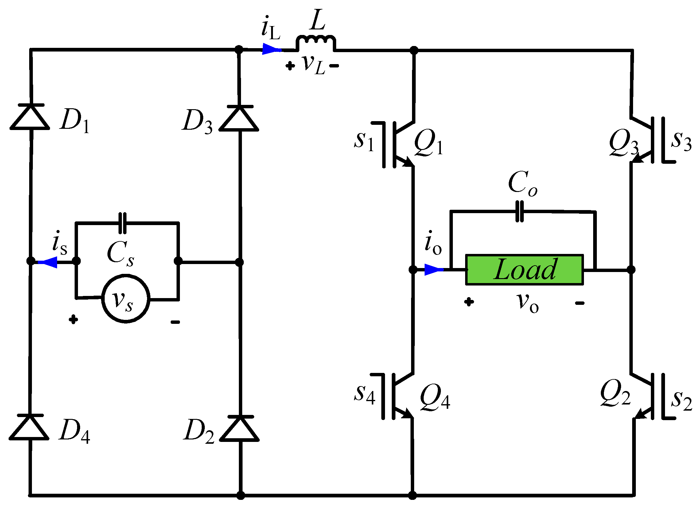
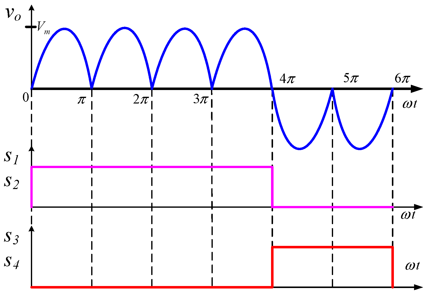
2. Operating Principle of the Tested Circuit

This section briefly describes the generation of various output pulses, exploring the conversion of AC power to DC by maintaining inverted and non-inverted arrangements of half cycles of the source voltage at the output in a specific manner. At the same time, it retains the sinusoidal characteristics of the source current. These outputs can be generated from various circuits, and one such simple topology, as presented in [23], is expressed in Figure 1.
This circuit consists of two H bridges separated by an inductor. The role of this inductor is to avoid the possible short-circuiting of the source voltage when all the transistors Q1 to Q4 of the second half of the circuit remain on. At the same time, it also serves as an energy-storing component for voltage boost operation.

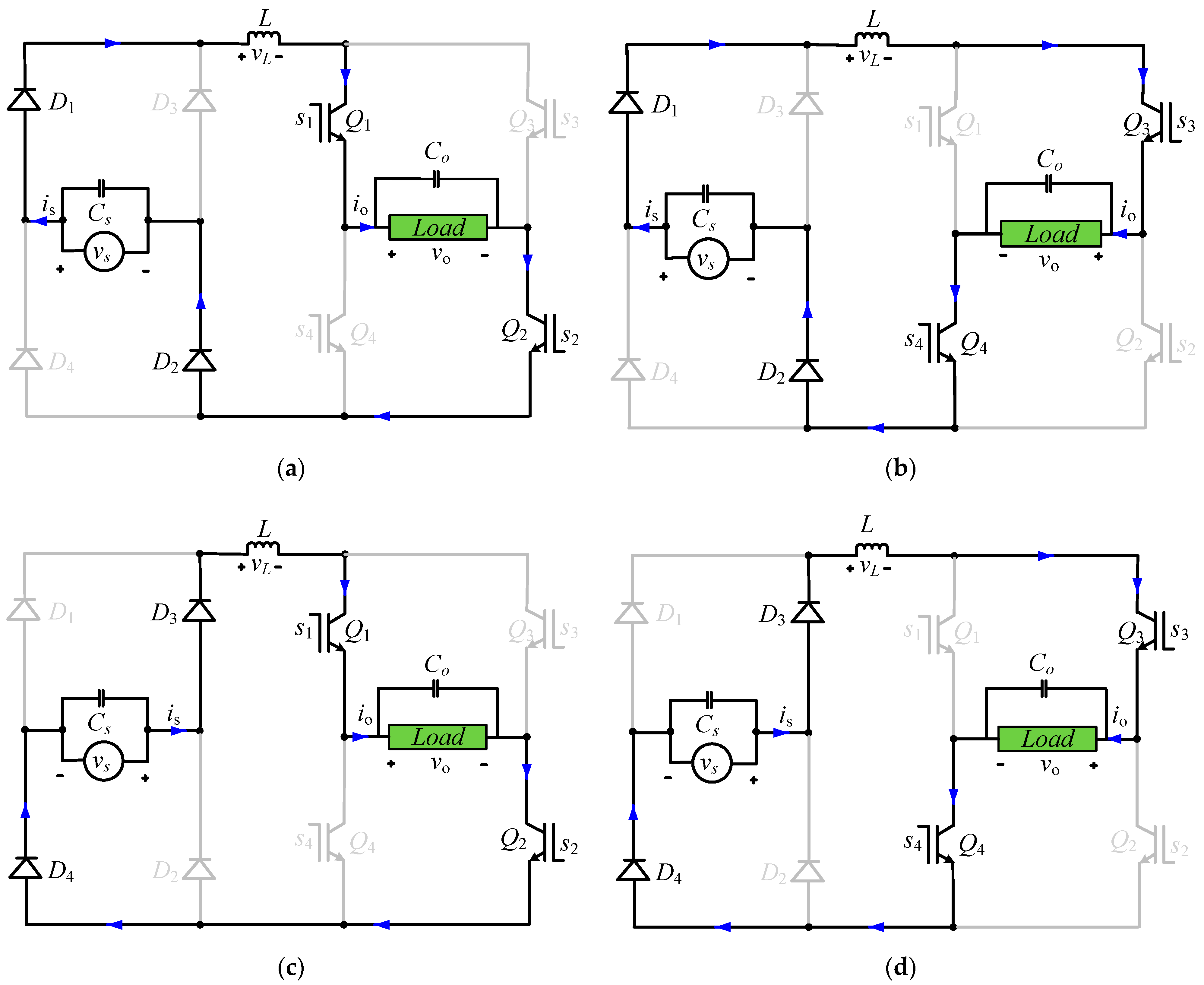
2.1. Equivalent Circuit Loops for Voltage Step-Down Operation

The output will be assumed to be positive or negative if the transistor pairs Q1, Q2 or Q3, Q4 are turned on, respectively. There is a big chance that transistor Q1 remains on with transistor Q4, and the same may be true for transistors Q3 and Q2. The front-end circuit of diodes D1 to D4 operates as a normal rectifier, converting the bidirectional input AC voltage to its unidirectional form, which is, by nature, a pulsating DC. In the present form of the diodes, their output is positive, but by reversing the direction of the diodes, the output may be converted into the negative form. Figure 2a–d show the equivalent circuit loops, indicating how the output voltage can be converted to its non-inverted and inverted forms.

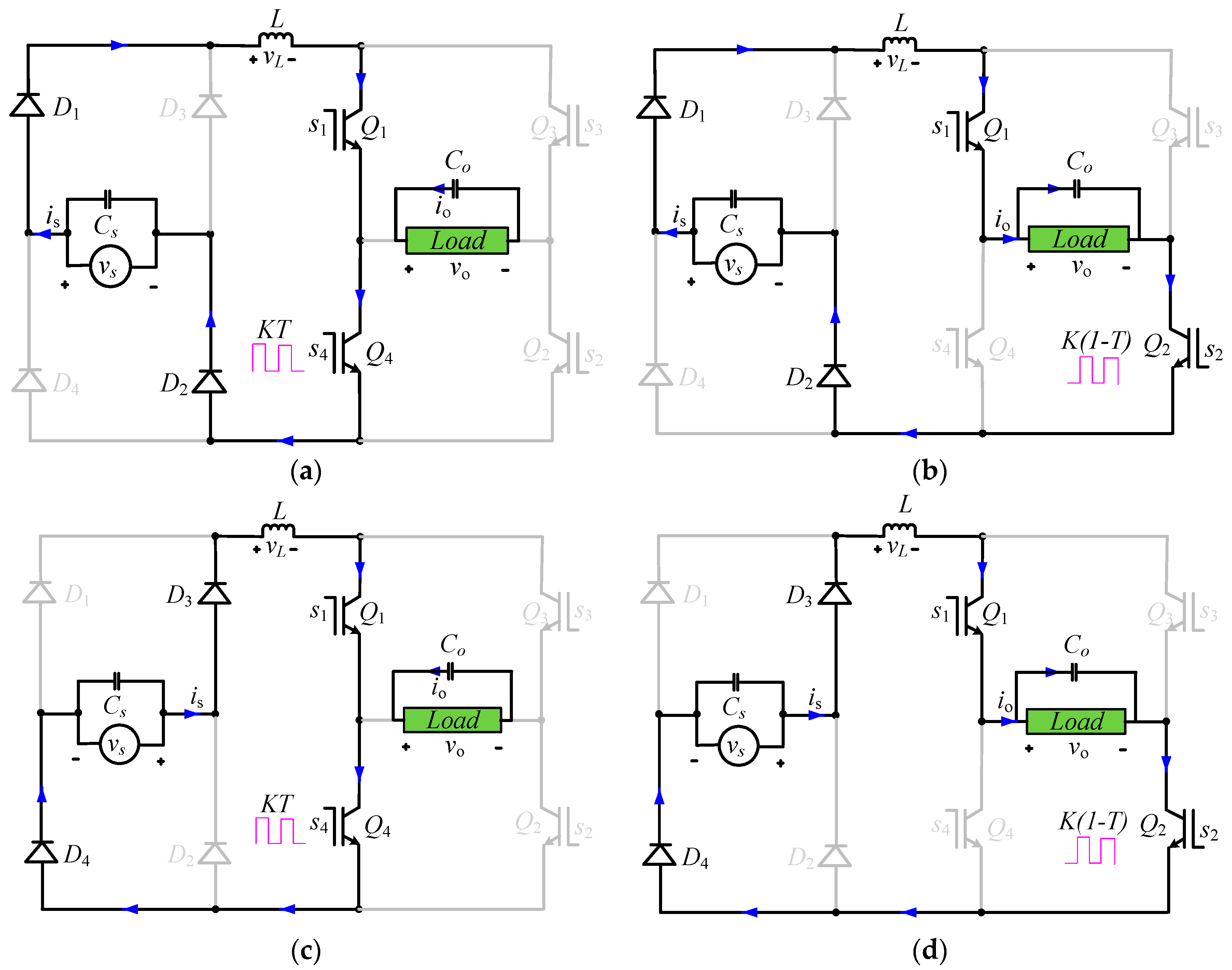
2.2. Equivalent Circuit Loops for Voltage Step-Up Operation

The presence of an inductor can also facilitate the boosting of the input voltage via the duty cycle control (K). Figure 3a–d show the equivalent circuit loops indicating how the output voltage can be controlled via duty cycle control. Figure 3a,c illustrate energy storage in the inductor L. During the PWM on-interval, the inductor is directly connected to the source voltage; therefore, it holds the value of the source voltage.
V L ( t = K T ) = V s
Figure 3b,d indicate the transfer of stored energy, ensuring the voltage boost’s operation. During the PWM off-interval, the inductor is connected between the output and input. So, its voltage drop is the difference between the input and output voltage.
V L ( t = ( 1 K ) T ) = V s V o
The principle of volt-second balancing can be used to determine the variation in the output voltage through PWM control.
V s K T = 1 K T V s V o
V o = V s 1 K
The main consideration for the operation of the circuit is to maintain the continuous flow of the power from source to load. The variation in the load DC voltage with such constraints of source current without employing filters is achieved by maintaining the output pulses with positive or negative values. This converter operates as a voltage boost regulator for high voltage regulation. So, it always maintains the continuity and sinusoidal characteristics of the input current. For voltage step-up, the instantaneous output half cycles are unipolar (all positive or negative depending on the load requirement), and their peak value is governed by duty cycle control. To obtain a step-down variation in the output DC voltage, the instantaneous output pulses are maintained in positive and negative values. Their peak is adjusted as per the output DC voltage requirement. The role of the number of instantaneous output half cycles or pulses can easily be explored with one example, where the number of output pulses is considered to be six. The output DC voltage can be regulated from positive to negative by playing with the polarity of the output pulses. The polarity of the output voltage pulse is assumed to be positive by turning transistors Q1 and Q2 and negative once Q3 and Q4 conduct it. Figure 4a shows output pulses to produce the maximum positive output DC voltage. Such an output can be created by turning on the transistors Q1 and Q2 of Figure 1. The output DC voltage can be reduced to zero by setting equal positive and negative output pulses, as may be seen in Figure 4d. For a zero output DC voltage requirement, the input current retains its sinusoidal behavior. The variation in the instantaneous output voltage may be easily viewed by glancing at the switching status of the operating transistors. The output is shown in Figure 4c, which represents four positive and two negative pulses that may be generated with control inputs shown in Figure 5.
The value of the DC voltage for the outputs of Figure 4a–d are calculated in Equations (5)–(8), respectively.
V D C = 1 6 π 0 π V m sin ω t d ω t π 2 π V m sin ω t d ω t + 2 π 3 π V m sin ω t d ω t 3 π 4 π V m sin ω t d ω t + 4 π 5 π V m sin ω t d ω t 5 π 6 π V m sin ω t d ω t = 2 V m π
V D C = 1 6 π 0 π V m sin ω t d ω t π 2 π V m sin ω t d ω t + 2 π 3 π V m sin ω t d ω t 3 π 4 π V m sin ω t d ω t + 4 π 5 π V m sin ω t d ω t + 5 π 6 π V m sin ω t d ω t = 4 V m 3 π
V D C = 1 6 π 0 π V m sin ω t d ω t π 2 π V m sin ω t d ω t + 2 π 3 π V m sin ω t d ω t 3 π 4 π V m sin ω t d ω t 4 π 5 π V m sin ω t d ω t + 5 π 6 π V m sin ω t d ω t = 2 V m 3 π
V D C = 1 6 π 0 π V m sin ω t d ω t π 2 π V m sin ω t d ω t + 2 π 3 π V m sin ω t d ω t + 3 π 4 π V m sin ω t d ω t 4 π 5 π V m sin ω t d ω t + 5 π 6 π V m sin ω t d ω t = 0
The output DC voltage of the above type of pulse is positive, as the area under such an output is positive. This is only true if the number of positive pulses is greater than the number of negative pulses. In an oppositive scenario, as shown in Figure 6, the output DC voltage is always negative. There are four, five and six negative pulses in Figure 6a–c respectively.
The values of the DC voltage for the outputs of Figure 6a–c are calculated in Equations (9)–(11), respectively.
V D C = 1 6 π 0 π V m sin ω t d ω t π 2 π V m sin ω t d ω t 2 π 3 π V m sin ω t d ω t + 3 π 4 π V m sin ω t d ω t 4 π 5 π V m sin ω t d ω t + 5 π 6 π V m sin ω t d ω t = 2 V m 3 π
V D C = 1 6 π 0 π V m sin ω t d ω t + π 2 π V m sin ω t d ω t 2 π 3 π V m sin ω t d ω t + 3 π 4 π V m sin ω t d ω t 4 π 5 π V m sin ω t d ω t + 5 π 6 π V m sin ω t d ω t = 4 V m 3 π
V D C = 1 6 π 0 π V m sin ω t d ω t + π 2 π V m sin ω t d ω t 2 π 3 π V m sin ω t d ω t + 3 π 4 π V m sin ω t d ω t 4 π 5 π V m sin ω t d ω t + 5 π 6 π V m sin ω t d ω t = 2 V m π
Similarly, by controlling the number of output pulses with controlled peak values, the variation in the output DC voltage can also be further modulated.

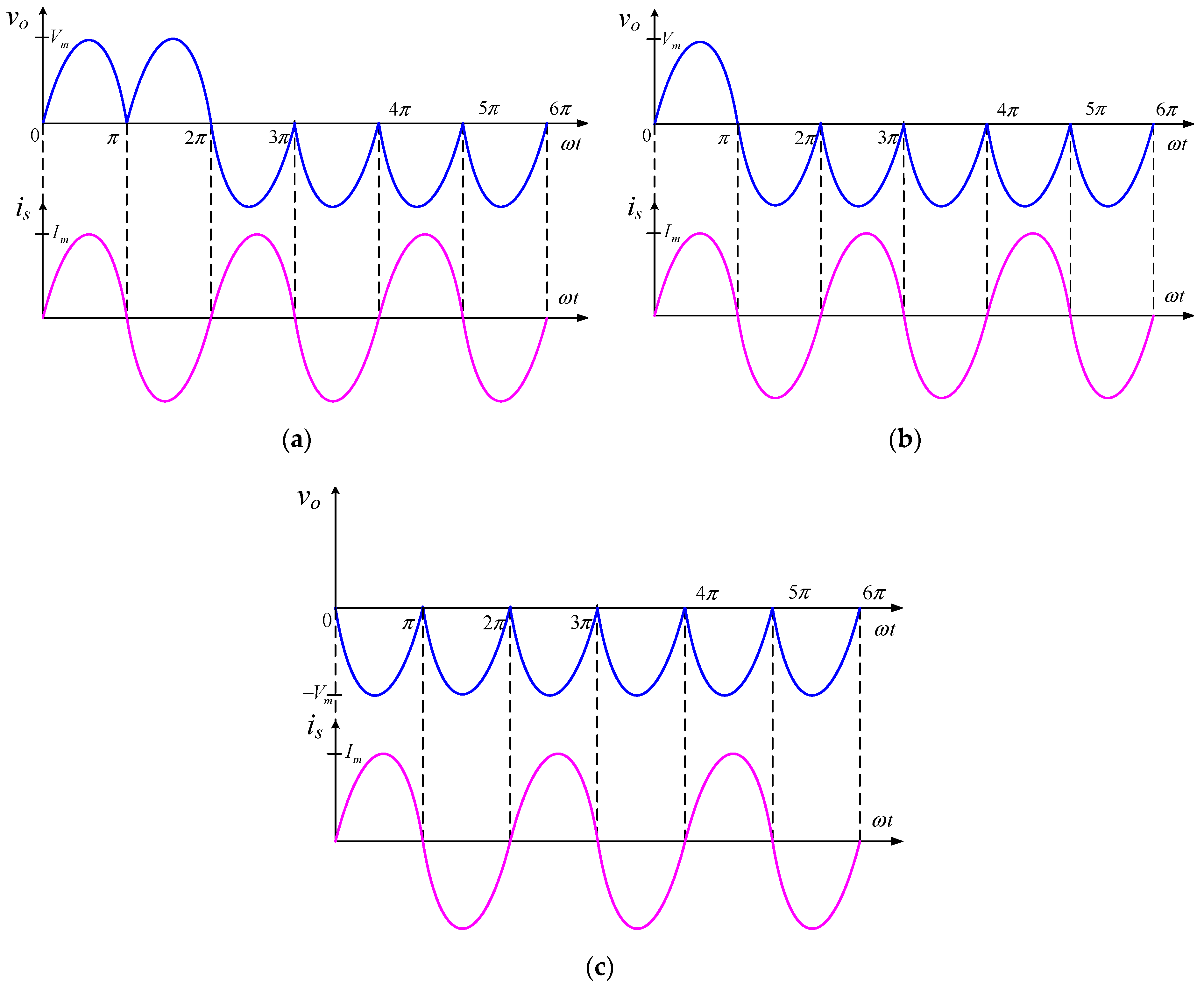
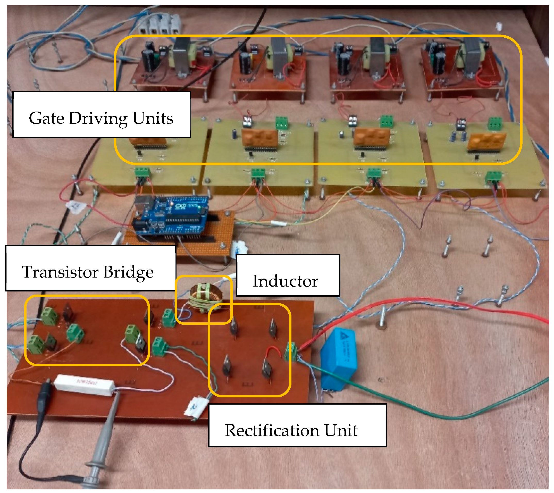
3. Evaluation and Examination

The main focus of this work is related to harmonics minimization in the source current by controlling the output DC voltage. For simplicity, let us select a resistive load because it describes the high distortion in the source current. The harmonic coefficients of the following arbitrary input current waveform seen in Figure 7 are calculated below.
a n ( n 1 ) = 2 I m π n 2 1 + I m π n + 1 cos n α + α I m π n 1 cos n α α     f o r     n = 3 , 5 , 7 ,
b n ( n 1 ) = I m π n + 1 sin n α + α I m π n 1 sin n α α   f o r     n = 3 , 5 , 7 ,
a n ( n = 1 ) = I m 2 π cos n α 1
b n ( n = 1 ) = I m π π α + 1 2 sin 2 α
These coefficients are combined to obtain the instantaneous behavior in mathematical form.
i s ( ω t ) = I m π π α sin ω t + I m 2 π cos ω t 2 α cos ω t + I m π n 1 cos n ω t cos n ω t n α + α I m π n + 1 cos n ω t cos n ω t n α α     f o r   n = 3 , 5 , 7 ,
The first term in the above equation is the required fundamental components, and its peak value is scaled by the factor of (πα)/π, and its value can only be maximum for α = 0. The remaining terms of this equation are unwanted means harmonics, and they can only be eliminated by putting the value of the firing delay angle at zero. Therefore, for a zero firing delay angle, the input current waveform of Figure 7 is improved to a sinusoidal waveform, and this characteristic may also be confirmed by an inspection of Equation (16). The output DC voltage may be linked to duty cycle control (α) for the resistive load.
V D C = V m π 1 + cos α
The maximum DC voltage of 2Vm/π is gained with a zero firing delay angle, and this is the only case in which the harmonic components of the input current are zero. For DC voltage regulation, the value of the firing delay angle is always non-zero. This lowers the peak value of the current fundamental component and increases the amplitude of the harmonics. This leads to a decrease in the displacement power factor (DPF) and total power factor (PF) and an increase in total harmonic distortion (THD) or total demand distortion (TDD), which are represented in mathematical form as
V D C = V m π 1 + cos α
D P F = cos α
T H D = I h I s 1
The time-varying characteristics of the input current in the suggested approach always remain sinusoidal, and hence, it improves the power factor and THD. Such an analysis may be observed with the data presented in Table 1.
This comparative study and observation validate the improvement in the power quality measures of the input current for similar output voltage characteristics.

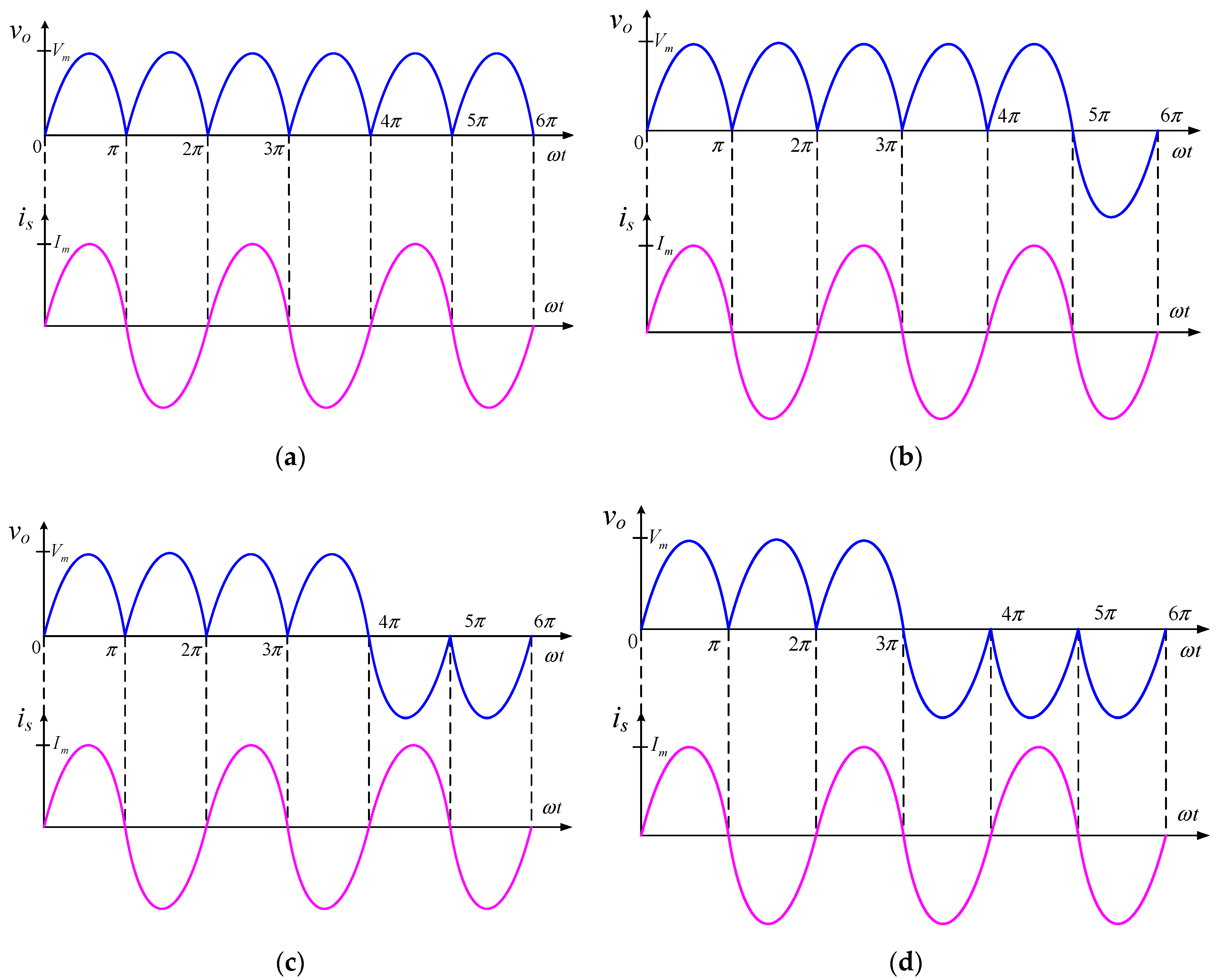
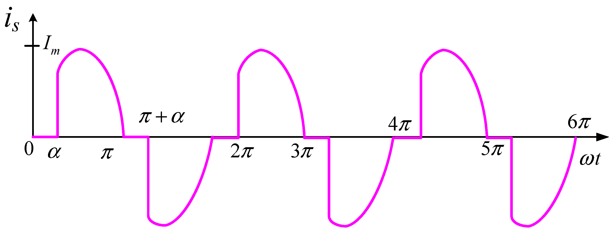
4. Results and Argument

This section discusses how the characteristics of the input current with the proposed control strategy remain sinusoidal. The recorded results with the computer-dependent simulation and practical platform support the research’s validation.

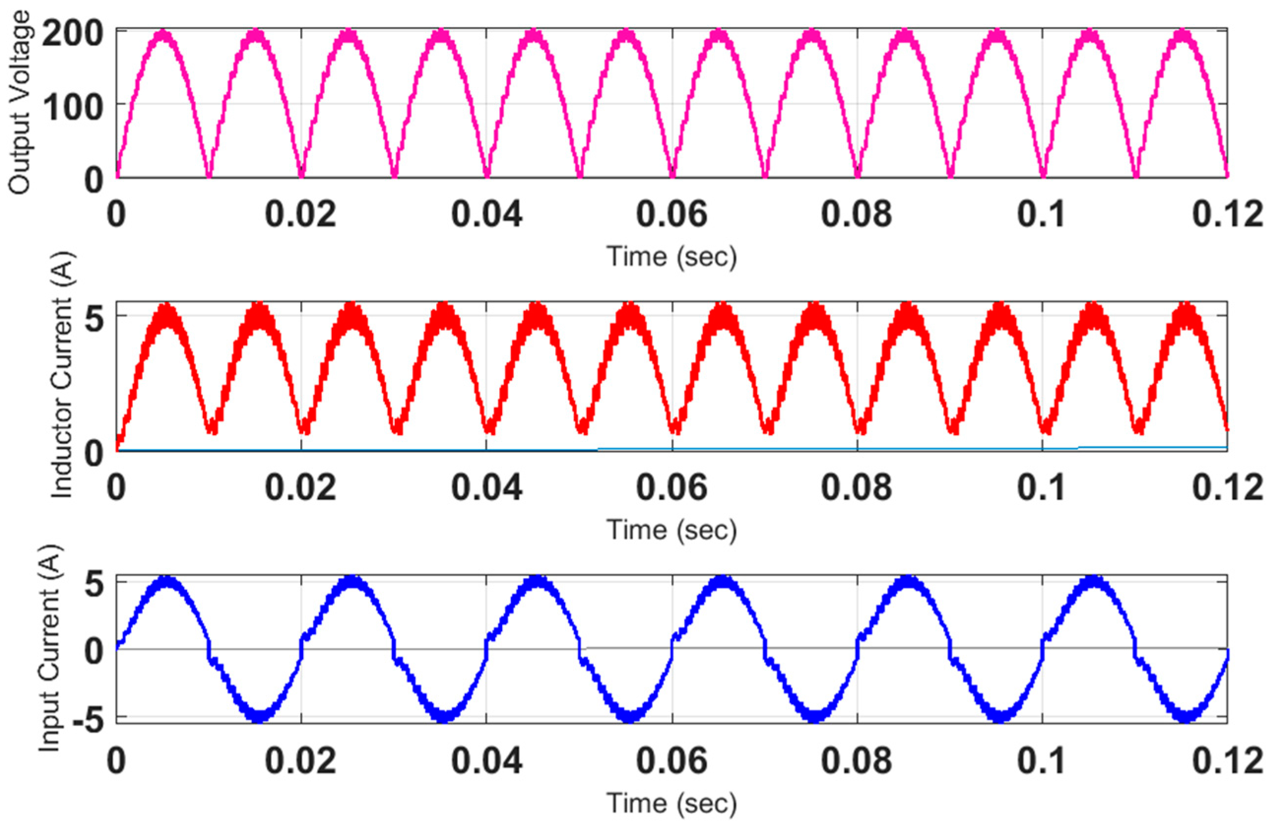
4.1. Discussion Based on Simulation Results

For computer simulation results, we employ the MATLAB R2021b (Simulink) platform for software results, as it is one of the most powerful full tools for the analysis and validation of power electronics circuits. Transistor models, measuring blocks, and passive components are selected as desired. A combination of pulse generators with mathematical operators is employed for the generation of gating signals. The peak value of the input source voltage is set to 150 V at a 50 Hz frequency for the validation of the voltage step-down operation. For a voltage boost output of either polarity (positive or negative), all output pulses have unipolarity, and regulation of the DC output voltage is gained with the high-frequency PWM control. In this mode of operation, the features of the source current remain sinusoidal except for some percentage of ripple, which may bring an acceptable level with the appropriate inductor design and switching frequency. The value of the inductor depends on the acceptable ripple factor (kir), duty cycle control, peak value of the input voltage and current, and switching frequency. These values are taken as 20%, 0.5, 200 V, 10 A, and 25 kHz, respectively, for the inductor design.
L =   k V s k i r I L f s   = 2     mH
Similarly, the design of the output filter may be obtained for k = 0.5, Io = 5 A, Kvr = 0.1, Vo = 300 V, and fs = 25 kHz.
C o =   k I o k v r V o f s   = 3.33     μ F
The waveform of the input current for the output voltage of a 200 V peak is shown in Figure 8 for resistive load.
Inductive load requires active and reactive power that may create a phase difference between the output voltage and output current. A small-value capacitor is connected across the load. This capacitor not only helps in the suppression of ripples of the output voltage but also provides the reactive power demanded by the inductive nature of the load. As a result, there is no significant increase in the phase angle between the input voltage and current. Figure 9 shows the instantaneous value of the output voltage inductor and input current for an inductive load.
The detailed analysis of Figure 8 and Figure 9 explores that there is an increase in the instantaneous load voltage, inductor current, and input current.
The other major focus of this section is to explore the number of half cycles with bipolar polarity to adjust the output DC voltage in voltage step-down by ensuring the sinusoidal features of the source current. The total number of output pulses and their polarities determine the DC output voltage. For example, consider the selection of four positive and two negative output half cycles. In this case, the DC value of the two negative half-cycles is canceled out with the DC value of two positive half-cycles. In this case, only two positive half cycles are responsible for the output DC voltage for the period of 6 π , and its value is computed in Equation (7) as 2Vm/3π. Its numerical DC value for a peak input voltage of 150 V is approximately 32 V, which is much less than the input peak voltage. Figure 10 shows the results for such an output with a resistive load.
Figure 11 shows the instantaneous value of the output voltage inductor and input current for an inductive load.

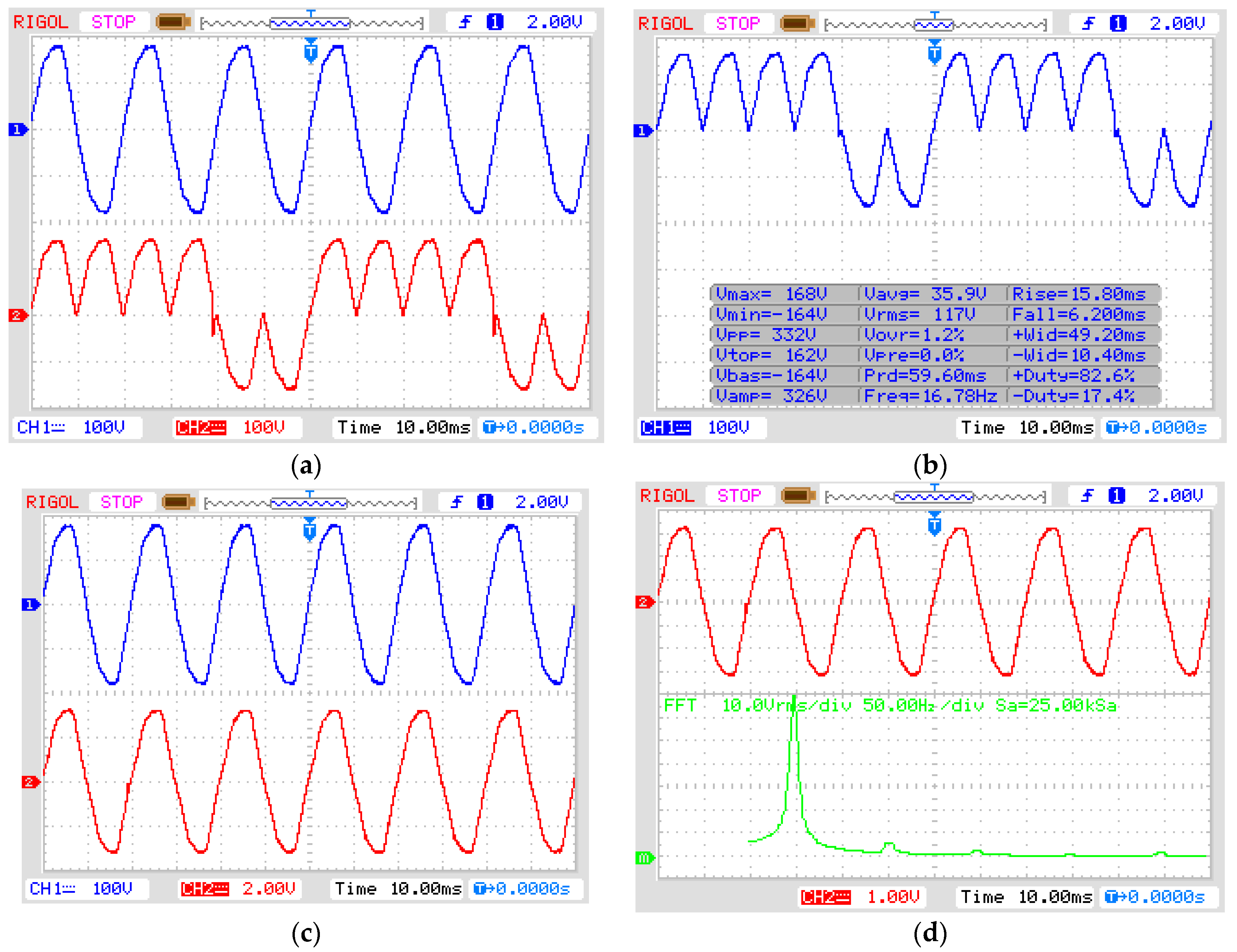
4.2. Discussion Based on Practical Results

The practical setup adopted from [23] for the implementation of the proposed topology is displayed in Figure 12. In the figure, the first H-bridge rectification unit is built with four diodes (RHRG3040), having abrupt reverse recovery characteristics. The second H-bridge is built with four transistors (IRF840), having low rise and fall times. It is used to arrange the various forms of the output pulses. As four switching transistors are used, so four gate control circuits are required to control their on and off states. Each gate control unit consists of an isolated DC power supply and hybrid chip (EXB840), which provides the electrical isolation between the low-voltage control unit and high-voltage power circuit. The connection of the inductor between these two H-bridges avoids the parallel connection of input and output capacitors. It also serves as an energy-storing component for boost operation. The practical results are achieved with a dual-channel RIGOL oscilloscope. These channels are used for the practical plotting of two separate signals.
Various forms of the output pulses are presented and discussed. Figure 13a shows an output consisting of six pulses. Five of them are positive and one is negative in this waveform, as shown in red. The maximum value of the input voltage waveform is 166 V, and its period is assumed to be 2 π . The DC value of one negative pulse is canceled out with one of the positive ones. The total DC voltage of this output waveform is equal to four half cycles in a period of 6 π . The DC value of the first half cycle in a given period (6 π ) is computed at 17.613 V. As there are four pulses or half cycles, the total DC is obtained by multiplying by four, which is approximately 70.45. This value may be confirmed by the practical recorded result of Figure 13b or the mathematically computed value of Equation (6). It may also be viewed from Figure 13c,d that the input current retains its sinusoidal behavior, ensuring a good power quality for the source-side current.
Figure 14a shows a similar output voltage waveform but with two negative half cycles. The total DC voltage of this output waveform is equal to two half cycles in a period of 6 π . The DC value of the first half cycle in a given period (6 π ) is computed at 17.613 V. As there are such two pulses or half cycles, the total DC is obtained by multiplying by two, which is approximately 35.22. This value may be confirmed by the practical recorded result of Figure 14b. It may also be viewed from Figure 14c,d that the input current retains its sinusoidal behavior, ensuring a good power quality for the source-side current.
It is observed that the output DC voltage of Figure 13 is double the DC voltage of Figure 14. The output voltage between these values may also be changed by changing the number of output half cycles. Figure 15a shows the output of four half cycles, where three half cycles are positive and one is negative. The total DC voltage of this output waveform is equal to two half cycles in a period of 4 π . The DC value of the first half cycle in a given period (4 π ) is computed as 26.42 V. As there are such two pulses or half-cycles, the total DC is obtained by multiplying by two, which is approximately 52.83. This value may be confirmed by the practical recorded result of Figure 15b or the mathematically computed value of Equation (6). It may also be viewed from Figure 15c,d that the input current retains its sinusoidal behavior, ensuring a good power quality for the source-side current.
The critical observation and analysis of all the above results show that the output DC voltage may be regulated to some selected value with the specific polarity arrangement in the waveform of the output pulses. At the same time, the characteristics of the input current remain sinusoidal, ensuring an improved displacement power factor, total harmonic distortion, and overall power factor.

5. Conclusions

This paper presents a simple and novel control strategy for regulating the DC voltage in a single-phase full-wave circuit based on the voltage polarity control of the output pulses. The output voltage polarity control is created with the help of the non-inverting and inverting features of the switching power electronics circuits. The output DC voltage can be set to a positive or negative value with an adjustment of the number of half cycles of the input voltage at the output with a positive or negative polarity. In this whole process, the characteristics of the input source current remain continuous and sinusoidal, maintaining an acceptable power quality. This enhancement in power quality characteristics is validated by computing certain performance parameters like the displacement power factor, total power factor, and total harmonic distortion. The recorded waveforms of the input current also explore its sinusoidal characteristics. The results gained from simulation modeling and practical test circuits match their instantaneous characteristics. Practically recorded FFT plots confirm the improvements in the power quality of the input current, as no significant harmonic components are present in their frequency spectrum. With these characteristics, the THD of the input current is approximately less than 3%, and the power is approaching its maximum value for the various output voltages.

Author Contributions

Conceptualization, N.A.; Data curation, N.A.; Formal analysis, T.Y.; Methodology, N.A. and G.A.; Resources, G.A.; Validation, G.A.; Visualization, T.Y.; Writing—original draft, N.A.; Writing—review and editing, G.A. All authors have read and agreed to the published version of the manuscript.

Funding

This research received no external funding.

Institutional Review Board Statement

Not applicable.

Informed Consent Statement

Not applicable.

Data Availability Statement

The original contributions presented in the study are included in the article, further inquiries can be directed to the corresponding author.

Acknowledgments

The authors acknowledge and are thankful to the Department of Electrical Engineering, the University of Lahore, Pakistan, for providing the facilities to conduct this research.

Conflicts of Interest

The authors declare no conflicts of interest.

References

  1. Bajaj, M.; Singh, A.K. Grid integrated renewable DG systems: A review of power quality challenges and state-of-the-art mitigation techniques. Int. J. Energy Res. 2020, 44, 26–69. [Google Scholar] [CrossRef]
  2. Singh, B.; Singh, S.; Chandra, A.; Al-Haddad, K. Comprehensive Study of Single-Phase AC-DC Power Factor Corrected Converters with High-Frequency Isolation. IEEE Trans. Ind. Inform. 2011, 7, 540–556. [Google Scholar]
  3. Sharifi, S.; Monfared, M.; Nikbahar, A. Highly Efficient Single-Phase Direct AC-to-AC Converter with Reduced Semiconductor Count. IEEE Trans. Ind. Electron. 2021, 68, 1130–1138. [Google Scholar] [CrossRef]
  4. Sayed, S.S.; Massoud, A.M. Review on State-of-the-Art Unidirectional Non-Isolated Power Factor Correction Converters for Short-/Long-Distance Electric Vehicles. IEEE Access 2022, 10, 11308–11340. [Google Scholar]
  5. Vardani, B.; Tummuru, N.R. A Single-Stage Bidirectional Inductive Power Transfer System with Closed-Loop Current Control Strategy. IEEE Trans. Transp. Electrif. 2020, 6, 948–957. [Google Scholar]
  6. Baek, J.; Kim, J.-K.; Lee, J.-B.; Park, M.-H.; Moon, G.-W. A New Standby Structure Integrated with Boost PFC Converter for Server Power Supply. IEEE Trans. Power Electron. 2019, 34, 5283–5293. [Google Scholar]
  7. Wei, Y.; Luo, Q.; Alonso, J.M.; Mantooth, A. A Magnetically Controlled Single-Stage AC–DC Converter. IEEE Trans. Power Electron. 2020, 35, 8872–8877. [Google Scholar]
  8. Ponce-Silva, M.; Salazar-Pérez, D.; Rodríguez-Benítez, O.M.; Vela-Valdés, L.G.; Claudio-Sánchez, A.; De León-Aldaco, S.E.; Cortés-García, C.; Saavedra-Benítez, Y.I.; Lozoya-Ponce, R.E.; Aquí-Tapia, J.A. Flyback Converter for Solid-State Lighting Applications with Partial Energy Processing. Electronics 2020, 10, 60. [Google Scholar] [CrossRef]
  9. Dini, P.; Saponara, S. Modeling and Control Simulation of Power Converters in Automotive Applications. Appl. Sci. 2024, 14, 1227. [Google Scholar] [CrossRef]
  10. Sadeghian, O.; Oshnoei, A.; Mohammadi-ivatloo, B.; Vahidinasab, V.; Anvari-Moghaddam, A. A comprehensive review on electric vehicles smart charging: Solutions, strategies, technologies, and challenges. J. Energy Storage 2022, 54, 105241. [Google Scholar]
  11. Zhang, L.; Yin, Q.; Zhu, W.; Lyu, L.; Jiang, L.; Koh, L.H.; Cai, G. Research on the orderly charging and discharging mechanism of electric vehicles considering travel characteristics and carbon quota. IEEE Trans. Transp. Electrif. 2023, 10, 3012–3027. [Google Scholar] [CrossRef]
  12. Amin, A.; Tareen, W.U.K.; Usman, M.; Ali, H.; Bari, I.; Horan, B.; Mekhilef, S.; Asif, M.; Ahmed, S.; Mahmood, A. A Review of Optimal Charging Strategy for Electric Vehicles under Dynamic Pricing Schemes in the Distribution Charging Network. Sustainability 2020, 12, 10160. [Google Scholar] [CrossRef]
  13. Li, C.; Xu, D. Family of Enhanced ZCS Single-Stage Single-Phase Isolated AC–DC Converter for High-Power High-Voltage DC Supply. IEEE Trans. Ind. Electron. 2017, 64, 3629–3639. [Google Scholar] [CrossRef]
  14. Ashraf, N.; Abbas, G.; Abbassi, R.; Jerbi, H. Power Quality Analysis of the Output Voltage of AC Voltage and Frequency Controllers Realized with Various Voltage Control Techniques. Appl. Sci. 2021, 11, 538. [Google Scholar] [CrossRef]
  15. Ibrahim, M.E.; Abd-Elhady, A.M. Power frequency AC voltage measurement based on double wound Rogowski coil. High Volt. 2017, 2, 129–135. [Google Scholar] [CrossRef]
  16. Ashraf, N.; Izhar, T.; Abbas, G.; Yasin, A.R.; Kashif, A.R. Power quality analysis of a three phase ac-to-dc controlled converter. In Proceedings of the 2017 International Conference on Electrical Engineering (ICEE), Lahore, Pakistan, 2–4 March 2017; pp. 1–6. [Google Scholar]
  17. Friedli, T.; Hartmann, M.; Kolar, J.W. The Essence of Three-Phase PFC Rectifier Systems—Part II. IEEE Trans. Power Electron. 2014, 29, 543–560. [Google Scholar] [CrossRef]
  18. Jain, A.; Gupta, K.K.; Jain, S.K.; Bhatnagar, P. A Bidirectional Five-Level Buck PFC Rectifier with Wide Output Range for EV Charging Application. IEEE Trans. Power Electron. 2022, 37, 13439–13455. [Google Scholar] [CrossRef]
  19. Yang, X.; Zhang, Z.; Xu, M.; Li, S.; Zhang, Y.; Zhu, X.F.; Ouyang, X.; Alù, A. Digital non-Foster-inspired electronics for broadband impedance matching. Nat. Commun. 2024, 15, 4346. [Google Scholar] [CrossRef]
  20. Ghanayem, H.; Alathamneh, M.; Yang, X.; Seo, S.; Nelms, R.M. Enhanced Three-Phase Shunt Active Power Filter Utilizing an Adaptive Frequency Proportional-Integral–Resonant Controller and a Sensorless Voltage Method. Energies 2024, 18, 116. [Google Scholar] [CrossRef]
  21. Boopathi, R.; Indragandhi, V. Enhancement of power quality in grid-connected systems using a predictive direct power controlled based PV-interfaced with multilevel inverter shunt active power filter. Sci. Rep. 2025, 15, 7967. [Google Scholar] [CrossRef] [PubMed]
  22. Zhang, Y.; Yang, X.; Zhang, Z. High-Efficiency Broadband Electroacoustic Energy Conversion Using Non-Foster-Inspired Circuit and Adaptively Switched Capacitor. IEEE Trans. Ind. Electron. 2025. [Google Scholar] [CrossRef]
  23. Ashraf, N.; Abbas, G.; Ullah, N.; Alahmadi, A.A.; Awan, A.B.; Zubair, M.; Farooq, U. A Simple Two-Stage AC-AC Circuit Topology Employed as High-Frequency Controller for Domestic Induction Heating System. Appl. Sci. 2021, 11, 8325. [Google Scholar] [CrossRef]
Figure 1. Employed circuit.
Energies 18 01674 g001
Figure 2. Equivalent circuit loops for voltage step-down operation: (a,c) Non-inverted outputs for positive and negative input. (b,d) Inverted outputs for positive and negative input.
Energies 18 01674 g002
Figure 3. Equivalent circuit loops for voltage step-up operation: (a,c) Inductor (L) energization for positive and negative input. (b,d) Energy transfer for positive and negative input.
Energies 18 01674 g003
Figure 4. Output pulses concerning the input current: (a) six positive pulses. (b) five positive and one negative pulses. (c) four positive and two negative pulses. (d) three positive and negative pulses.
Energies 18 01674 g004
Figure 5. Control signals for four positive and two negative output pulses.
Energies 18 01674 g005
Figure 6. Output pulses concerning the input current: (a) two positive and four negative pulses. (b) one positive and five negative pulses. (c) six negative pulses.
Energies 18 01674 g006
Figure 7. Instantaneous input current waveform.
Energies 18 01674 g007
Figure 8. Instantaneous load voltage and source current for voltage step-up mode for resistive load.
Energies 18 01674 g008
Figure 9. Instantaneous load voltage, inductor, and source current for voltage step-up mode for inductive load.
Energies 18 01674 g009
Figure 10. Instantaneous load voltage and source current for voltage step-down mode for resistive load.
Energies 18 01674 g010
Figure 11. Instantaneous load voltage and source current for voltage step-down mode for inductive load.
Energies 18 01674 g011
Figure 12. Practical setup.
Energies 18 01674 g012
Figure 13. Practical results of five positive and one negative pulse: (a) Output voltage waveform (red). (b) Output voltage with measured parameters values. (c) Source current waveform. (d) Practically recorded FFT of input current.
Energies 18 01674 g013
Figure 14. Practical results of four positive and two negative pulses: (a) Output voltage waveform (red). (b) Measured output voltage characteristics. (c) Source current waveform. (d) Practically recorded FFT of input current.
Energies 18 01674 g014
Figure 15. Practical results of three positive and one negative pulse: (a) Output voltage waveform (red). (b) Measured output voltage characteristics. (c) Source current waveform. (d) Practically recorded FFT of input current.
Energies 18 01674 g015
Table 1. Comparative study with firing delay angle control strategy.
ParametersProposed StrategyExisting Strategy
Output DC VoltageEqualEqual
Output RMS VoltageInput RMS VoltageInput RMS Voltage
Bipolar Voltage FacilityYesNo
Displacement Power factorHighLow
Total Power FactorHighLow
Total Harmonic FactorLowHigh
Disclaimer/Publisher’s Note: The statements, opinions and data contained in all publications are solely those of the individual author(s) and contributor(s) and not of MDPI and/or the editor(s). MDPI and/or the editor(s) disclaim responsibility for any injury to people or property resulting from any ideas, methods, instructions or products referred to in the content.

