1. Introduction
The process of converting light energy into electrical energy is achieved via a process known as the photovoltaic (PV) effect [
1]. A PV cell is used to harvest light energy and convert it into electric energy for powering electronic devices. A PV module is formed by connecting multiple PV cells in series and parallel to meet the power requirements of different electrical loads. There are different PV technologies, which include first-generation silicon-based PVs, second-generation thin-film-based PVs, such as copper indium gallium selenide (CIGS), cadmium telluride (CdTe), etc., and emerging third-generation PVs, such as perovskite solar cells (PSCs), organic PVs (OPVs), dye-sensitized solar cells (DSSCs), etc. Among all PV technologies, PSCs have drawn significant attention recently. The record-certified power conversion efficiency (PCE) of PSCs has risen to 27.0% under 1 sun (1000 W/m
2), comparable to other well-established PVs such as silicon-based solar cells [
2]. PSCs also exhibit superior performance under indoor lighting conditions due to the tunability of their bandgap and the high absorption coefficient of halide perovskite materials [
3]. By adjusting the PSC composition, the bandgap of perovskite can be tailored to better match the spectra of indoor illumination and thus maximize light absorption. In contrast, crystalline silicon has an indirect bandgap of 1.1 eV, which cannot be flexibly adjusted to optimally match the varied spectra encountered in indoor lighting environments. In addition, crystalline silicon exhibits intrinsically poor light absorption relative to direct bandgap materials like halide perovskites. The remarkable optoelectronic properties of PSCs give them an advantage over conventional silicon PVs for indoor light harvesting [
4]. Therefore, PSCs have great potential to address the demand for self-powered devices under low-illuminance conditions, making them desirable for IoT applications, such as autonomous sensors and communication beacons for data sharing between multiple devices and systems across the internet. The IoT is a term used to describe objects that automatically and wirelessly communicate with other electronic devices. For self-sustainable IoT applications, the use of PVs offers a long-term power source compared to using non-rechargeable batteries alone. PVs can power IoT devices autonomously when incorporated with rechargeable batteries, which can prevent drawbacks due to high maintenance costs and network interruptions during periodic battery replacement [
5]. Diverse applications, including sensors [
6], self-sufficient IoT [
7,
8], healthcare [
9], and industrial process monitoring, have found worthwhile benefits from the development of an efficient energy harvesting system (EHS) incorporating PSCs.
PSCs, like other PV technologies, suffer from nonlinear power generation under varying irradiance conditions. Directly connecting a load to PV modules and energy storage without carefully designing and optimizing the EHS is not the optimal configuration for applications involving fluctuating light levels. Therefore, implementing an MPPT algorithm is required to optimize the performance of the PSC-based EHS operating under variable indoor lighting conditions. The most common MPPT algorithms used in EHSs include the perturb and observe (P&O) [
10], hill-climbing [
11], and incremental conductance techniques [
12]. The MPPT control system aims to maximize the amount of power extracted from PVs by ensuring that the system functions at maximum power points under different irradiance conditions [
13].
Table 1 compares recent simulation studies focused on PV EHSs for indoor applications. Mishu et al. [
14] designed a hybrid EHS powered by an integrated PV and thermoelectric (TE) system for powering IoT sensors with an output power range of 0.14 W to 2.13 W under an indoor irradiance ranging from 50 lux to 200 lux. Their system demonstrated an improved output power efficiency compared to single-source-powered EHSs. It is noted that the proposed EHS used a supercapacitor for energy storage, which will cause a high self-discharge rate, leading to a short operation time. Kantareddy et al. [
15] proposed a novel PSC-powered radio-frequency identification (RFID) sensor that incorporated an onboard digital temperature sensor capable of wirelessly transmitting data over 4 m under high illumination. Wang et al. [
16] proposed high-efficiency charging circuitry for indoor IoT applications using PV panels with a supercapacitor as a backup energy storage system. The proposed system has an improved supercapacitor charging time efficiency of 64%, which shows that it is a promising alternative to the use of a battery. However, due to the quick discharge rate of the supercapacitor, the system cannot maintain a load demand voltage of 1.8 V for a longer period. Hence, to maintain a voltage level of 2 V to 4 V, a supercapacitor with a larger capacity is needed, but the PV system needs a longer time to charge the supercapacitor to 4 V. In a recent study by Wang et al. [
17], three different types of EHS circuitry using PSpice software (
https://www.orcad.com/products/orcad-pspice-designer/overview, (accessed on 26 February 2023)) were designed to improve the charging time of the supercapacitor to enhance the system’s capability to power IoT devices for a longer duration of time. These designs used the Joule Thief circuit, boost converter circuit, and capacitor stack circuit to meet the requirement for a long duration of operation. Meanwhile, Cheng et al. [
18] proposed a system designed using Hspice for IoT device applications, with a system architecture consisting of different parts (a pre-regulator circuit, an MPPT cross-coupled charge pump with a body selector, and power management circuits). The MPPT pump consisted of a sampling signal generation circuit, a sampling circuit, and a gated clock frequency modulation circuit. The chip design in the study allows for large, varied ranges of input voltages and throughput powers in small areas. Olzhabay et al. [
7] designed a PSC-powered EHS for uninterrupted IoT device application using LTspice software (XVII version). The proposed system used three series-connected and two parallel-connected PSC modules to enhance voltage output, while a fractional open-circuit voltage (FOCV) MPPT technique with the incorporation of a sample and hold circuit was employed to maximize energy extraction from PSC modules and stabilize voltage readings, respectively.
In this work, the P&O MPPT algorithm is implemented due to its low cost, easy implementation, and high tracking efficiency. Moreover, through the construction of a DC-DC boost converter, the PV voltage is scaled to the battery charging voltage. A bidirectional DC-DC buck–boost converter and a PI controller are used as the controlled battery management system. Incorporated with a PI controller, the bidirectional converter can adjust to changes in irradiance and optimize energy harvesting and storage. When the energy harvested from the PSCs experiences fluctuations due to unpredictable indoor lighting variations, implementing PI control in combination with a bidirectional converter enhances the charging of the energy storage element, which, in return, provides a steady power supply to IoT devices. Furthermore, the battery lifespan can be greatly improved by using a bidirectional converter and PI controller to prevent the battery from overcharging or deep draining and guarantee ideal charging cycles. Good battery management is crucial to support long-term IoT functionality in remote deployments where access for recharging or replacement is impractical. This article will explain the PSC architecture, the experimental fabrication of PSCs, the circuit architecture, and the modeling of a PSC-powered EHS in
Section 2.
Section 3 presents the simulation results obtained from the models.
Section 4 discusses the findings, while
Section 5 conclusively summarizes the key points.
2. Energy Harvesting System (EHS) Architecture
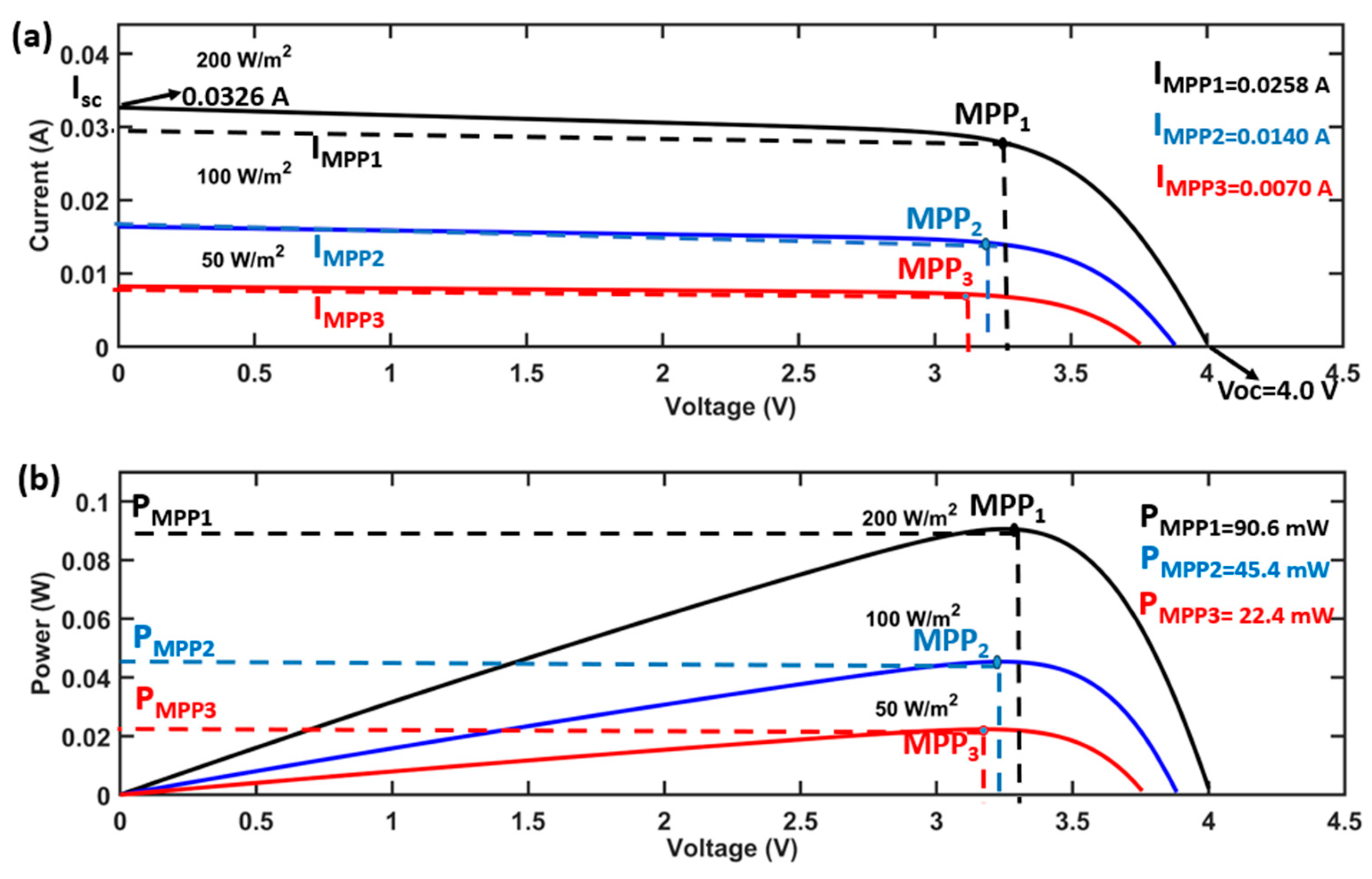
The proposed PSC-based EHS for IoT device indoor applications was designed for conditions under varying irradiance values of 200, 100, and 50 W/m
2. Depending on the time of day, indoor lighting throughout the day is often a combination of artificial lighting, such as fluorescent lamps, and natural light from the sun. The amount of sunlight that enters a room is determined by the size, angle, material type, and thickness of its windows. In the case of wide windows which extend the entire width of a room, distance and sun reflection are the primary causes of attenuation, or a gradual decrease in the intensity of solar irradiation. On a clear day, the average outdoor radiation levels are between 1000 W/m
2 and 325 W/m
2 [
19]. The radiance level decreases by 40% at one meter from a single window, resulting in values between 400 and 130 W/m
2 on clear and cloudy days, respectively. The radiance level drops even further at a wider distance of 5 m, resulting in a 93% decrease in the initial value of outdoor irradiance level. The reduction in radiance level for a double-glass-insulated window will be approximately 70% and 97%, respectively, at 1 and 5 m away from the window [
20,
21]. In this work, we used 200, 100, and 50 W/m
2 irradiance values, which are within a reasonable range for consideration under indoor conditions.
A bidirectional DC-DC buck–boost converter system with battery storage and a PSC module was modeled and simulated using MATLAB/Simulink (2023b).
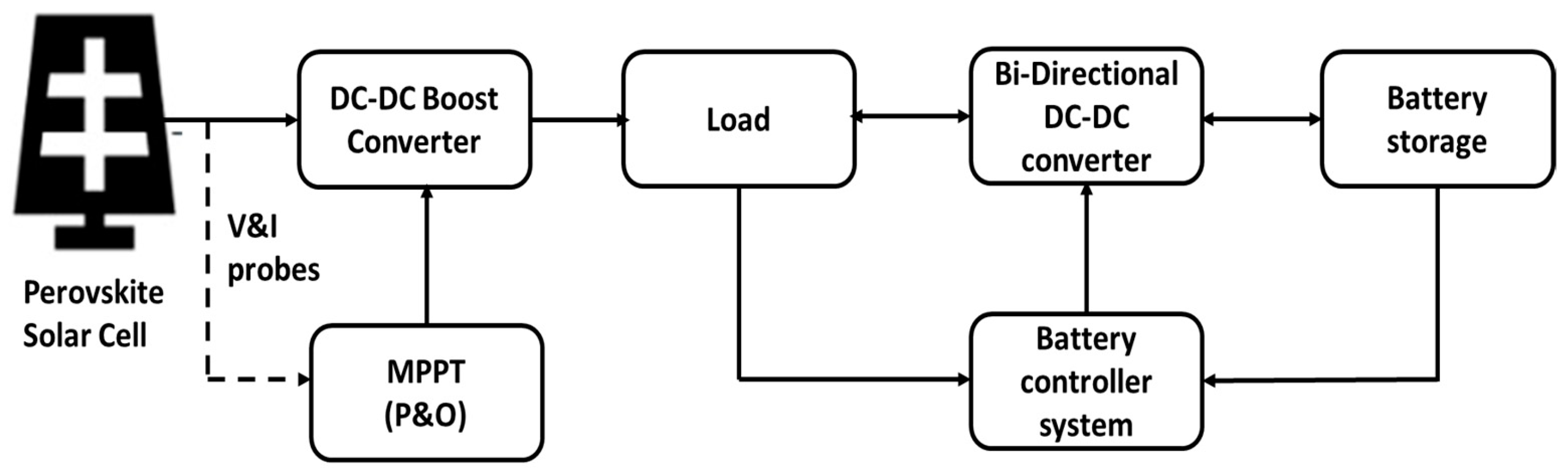
Figure 1 displays the block diagram of the proposed system with its circuit components. The output power and voltage from the PSC modules, consisting of one series-connected and four parallel-connected PSCs, are optimized by using the P&O MPPT technique. The DC-DC boost converter increases the input voltage from the PSC to the desired voltage level to charge the battery storage unit. At high irradiance, the energy generated from the PSC is enough to power the IoT load, while the surplus energy generated is stored by the battery system. However, when the energy generation of PSCs is insufficient in low-irradiation conditions, the battery supplies its stored energy to power the IoT load.
2.1. Fabrication of Perovskite Solar Cell (PSC)
The PCE of PSCs has significantly increased to 26.7% over the last decade [
2]. Their PCE is comparable to that of the well-known traditional silicon-based PVs. Furthermore, PSCs outperform established PV technology such as silicon solar cells in indoor environments with low-irradiance conditions [
8]. The light absorber of the PSC is made from halide perovskite materials with a structure of ABX
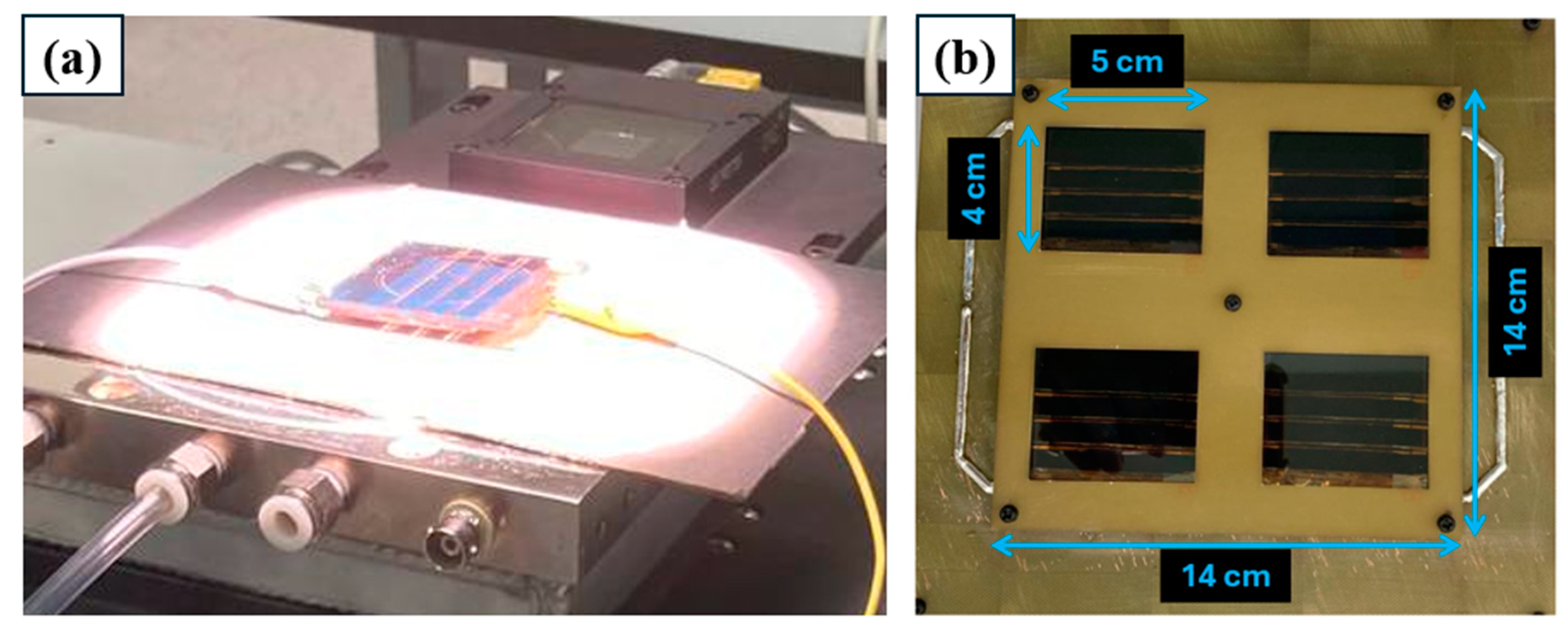
3—A: organic or inorganic cation such as methyl-ammonium, cesium (Cs), etc.; B: lead (Pb) or tin (Sn), and X: halides such as chlorine, iodine, or bromine. PSCs have received increasing attention in the field of indoor PVs because of their advantages, such as ease of production, bandgap adjustability, high defect tolerance, high absorption coefficients, high PCE, etc. Furthermore, the bandgap of perovskite materials can easily be controlled by adjusting their compositions. The tunability properties of PSCs allow the material absorption spectrum to be matched to the desired application. A PSC is composed of various functional layers that facilitate carrier transport across the layers, and these carriers are collected by the electrodes. Nevertheless, perovskite solar cells (PSCs) face significant challenges when scaled from laboratory-scale production to large-scale industrial applications. One major issue is the uniform deposition of perovskite layers across large areas, which can lead to defects, reducing overall efficiency and yield. However, the need for scalable and economical fabrication techniques continues to be a constraint, given that techniques such as roll-to-roll printing and blade coating, although promising, are not yet fully adapted for large-scale use without compromising cell efficiency. Also, durability is a critical challenge for PSCs, particularly in Internet of Things (IoT) applications where devices are expected to operate in diverse environmental conditions. PSCs are sensitive to moisture and air, both of which can degrade their performance over time. Strategies such as encapsulation have shown potential but add complexity and cost to the manufacturing process. The PSC used in this study was fabricated based on the method reported by Aidarkhanov et al. [
22]. The electron transport layer (ETL) consists of SnO
2 quantum dots and SnO
2 nanoparticles spin-coated in sequence. The active layer is mixed-cation and mixed-halide perovskite deposited via the antisolvent method inside a nitrogen-filled glove box. The PSCs were fabricated using a precursor solution composed of mixed cations and mixed halides. This solution was prepared by incorporating 0.2 mM PbBr
2, 1 mM FAI, 1.1 mM PbI
2, and 0.2 mM MABr into a 1 mL mixture of DMF and DMSO at a 4:1
v/
v ratio. The perovskite layer was deposited using the antisolvent method within a nitrogen-filled glove box. Spin coating was executed using a two-step process: first at 1000 rpm for 10 s, followed by 5000 rpm for 30 s. During the final 10 s of the second spinning step, 170 μL of CB was applied to the substrate. The substrate’s annealing temperature was 105 °C for 75 min. The hole transport layer (HTL) consisted of a Spiro-MeOTAD (Lumtec, Taipei, Taiwan) precursor solution, which was spin-coated within the glove box under an inert atmosphere. A gold electrode was thermally evaporated under a 10
−6 Torr vacuum.
2.2. DC-DC Boost Converter Modeling with P&O MPPT for PSC Module
The output voltage of the DC-DC converter is dependent on the duty cycle of the PV array and is immediately applied to the battery storage system for charging while also being controlled to the necessary voltage for the load [
10]. There are different types of DC-DC converters, namely, buck, boost, and buck–boost converters [
23]. To track the maximum power of the PSC module, a boost converter and P&O MPPT were deployed. By altering the duty signal of the converter, the module operating voltage can be controlled.
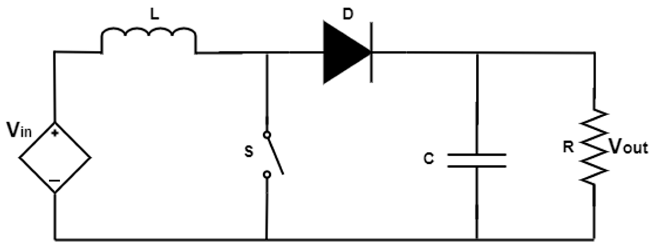
The DC-DC boost converter comprises an inductor (
L), a diode (
D), a capacitor (
C), a load resistor (
R), and a MOSFET control switch (
S), as shown in
Figure 2. This arrangement of the components (
Figure 2) allows for a step-up in the input voltage source (
Vin) at the output voltage (
Vout). Equation (1) states that the duty cycle of the control switch, D, or the ON time of the switch determines the relationship between these voltages [
24]:
By making the duty cycle (
D) the subject of the formula, we obtain the following equation:
The inductor (
L) value is determined by using the equation below, given that ∆
Il is the input ripple current value,
FS is the switching frequency, and the value of the ripple current should be between 20% and 30% of the input current [
25].
Finally, the capacitor (
C) value is calculated by considering the output ripple voltage, ∆
Vout, to be about 5% of the output voltage using Equation (4).
The load resistance value R was chosen so that the optimum resistance correlated with a duty cycle of
D = 50% when working under different irradiance conditions of 200 W/m
2, 100 W/m
2, and 50 W/m
2 at a constant temperature (T) = 25 °C. This computation was made using the following Equations (1)–(4) [
25].
2.3. Maximum Power Point Tracking (MPPT)
To operate PSCs at the global maximum, an MPPT system is deployed. This means that the PV maximum power output is achievable at a single operating point, which is referred to as the maximum power point (MPP) on the P-V characteristic curve. This point is always located at the turning point of the I-V curve and varies with the change in temperature and irradiation. The simplicity of P&O MPPT makes it a widely used approach for matching the MPP of PVs. This technique works by perturbing the PV module output voltage and comparing the PV output voltage to the output power of the previous irritation cycle [
26]. The drawback of the P&O MPPT method is that periodic changes in irradiance result in decreases in system efficiency [
27].
Figure 3 shows a flow chart for the P&O MPPT algorithm. In the P&O MPPT method, the operating voltage, V, or duty cycle,
D, is perturbed, and the new power, P (
n), is measured (calculation of probed current I (
n) and voltage V (
n)) and compared to the previous power, P (
n − 1). If the new power, P (
n), is greater than the previous power, the perturbation continues in the same direction. If P (
n) is less than P (
n − 1), the perturbation direction is reversed. The change in operational voltage V is achieved by changing the duty cycle,
D, with a duty cycle step size of Δ
D. This method aims to track the maximum power point (MPP) of the PV panel, but changes in irradiance can cause the system to oscillate around the MPP, reducing efficiency. Despite this drawback, P&O is widely used due to its computational simplicity, low cost, and ease of implementation [
28,
29].
2.4. Bidirectional DC-DC Buck–Boost Converter
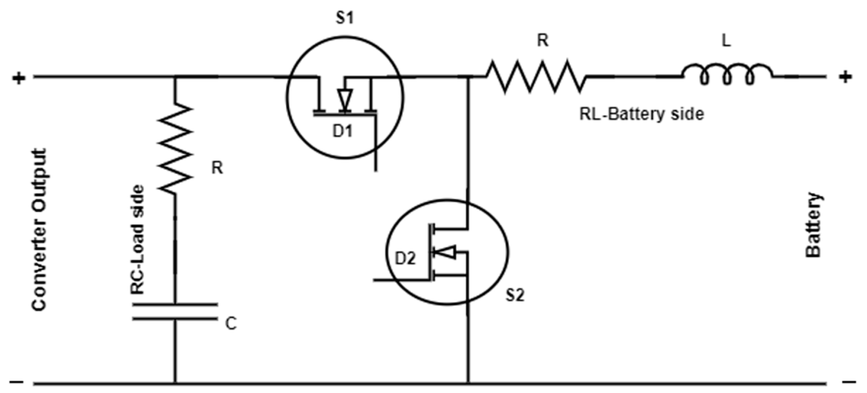
The bidirectional converter acts as the link between the PSC system and the battery storage and allows current to flow in two directions to the PSC system or the battery storage system. The bidirectional converter topology is presented in
Figure 4. This consists of passive energy storage components (inductor and capacitor) and MOSFET switches, which operate in two states: buck mode and boost mode [
30,
31]. In the buck converter state, the circuit functions in two modes when switch S1 is turned ON while S2 is turned OFF, resulting in diode D2 being turned ON while diode D1 is OFF. In this mode, the battery charges while the bidirectional charger circuit is in the buck operating mode because the irradiance level is insufficient to generate enough voltage required to drive the IoT load, causing current to flow from the battery system to the load, which is the discharge state.
Also, the bidirectional converter operates in a boost state when the battery storage is operating in a discharging state. Here, switches S1 and S2 are turned OFF and ON, respectively, and diode D1 is turned ON while diode D2 is turned OFF for the battery current to be discharged through an inductor. In this mode, the irradiance level is enough to produce the required voltage for the load, thereby resulting in a flow of current from the PV module to the battery storage system. The parameters of the bidirectional buck–boost converter are given in
Table 2.
2.5. Battery Storage System
The battery storage system can store electric charges, and when the battery is being charged by the PV module, the state-of-charge (SOC) for the battery increases (i.e., battery charging mode) and the SOC decreases when the battery powers the load (i.e., battery discharge mode). The battery used in this study has a battery-rated capacity of 35 mAh, and to simulate the battery charging and discharging scenarios, the SOC of the battery is varied. The battery charging and discharging rate is controlled by the bidirectional buck–boost converter. The battery operates within a nominal voltage range of 3.7–4.2 V with an internal resistance of 0.012 Ω.
Table 3 shows the modeling parameters for simulating Li-ion-based battery storage.
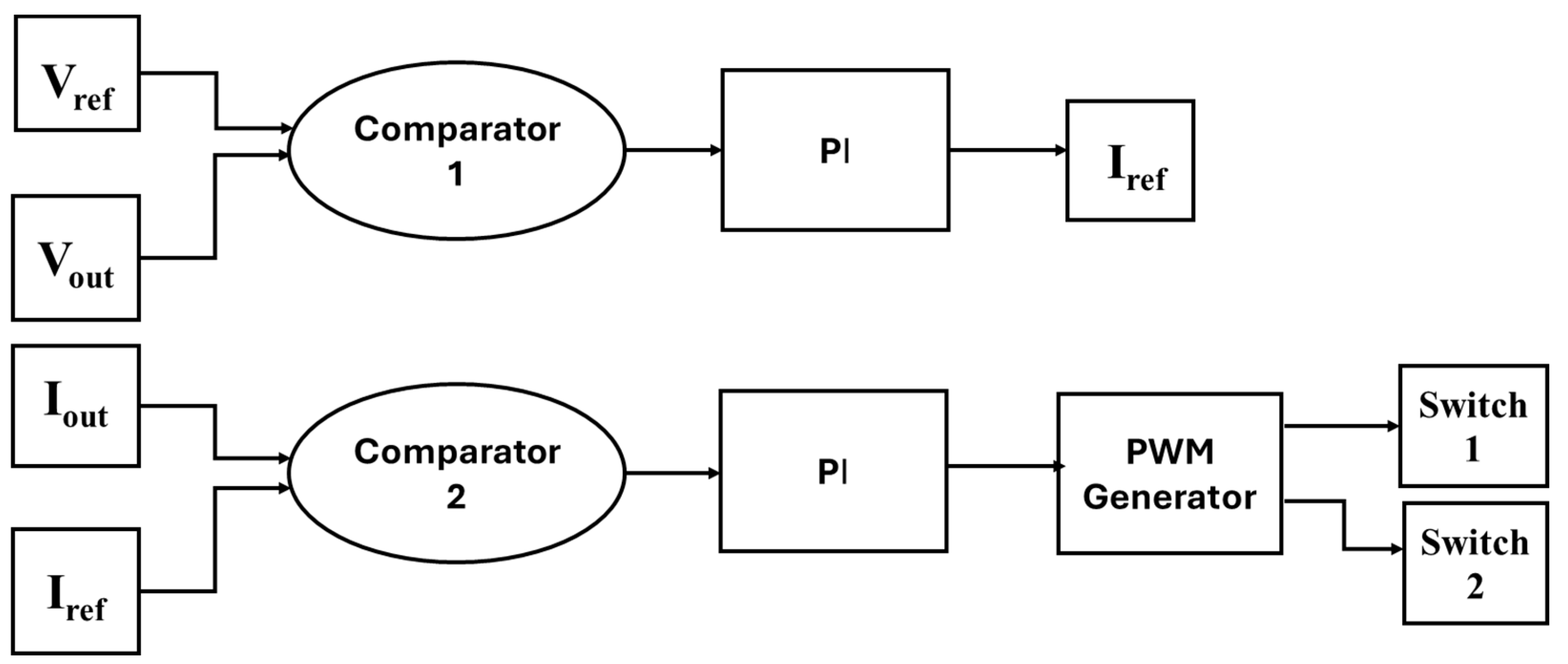
2.6. Battery Control Mechanism
To operate switches with the desired duty ratio, two PI controllers are employed in this work (refer to
Figure 5). A PI controller is a closed-loop feedback system that regulates process variables by manipulating the system variable based on the errors between the desired and actual outputs. The PWM generator that corresponds to the various PI controllers receives the output from the controller and then provides the necessary duty cycle to operate the switches. To switch on the boost converter and keep the PV module output voltage at the proper level, a second PI controller is utilized. Two types of controllers, voltage-controlled PI controller and current-controlled PI controller, are engaged to regulate the bidirectional DC-DC buck–boost converter [
32,
33]. The reference battery charging current is generated by a voltage-controlled PI controller. The actual voltage of the battery is determined by the output of the comparator, and the reference charging voltage is set at 4 V, which is approximately 95% of the fully charged voltage of 4.2 V. The voltage-controlled PI controller receives its input as an error signal from the comparator. The battery reference charging current is the voltage-controlled PI controller output. There will be a negative current during battery charging. Using a current-controlled PI controller, this created battery reference charging current is used to generate the necessary pulses for various switches.
Also, the battery charging current is used as feedback for the comparator of the current-controlled PI controller. The battery reference charging current is approximately −0.2 A. The difference between the desired and actual value (error) of the comparator will be used as input by the current-controlled PI controller. The DC-DC PWM generator receives its input from the output generated by the current-controlled PI controller. This will generate the necessary duty ratio for the operation of the bidirectional DC-DC buck–boost converter switches.
Table 4 shows the modeling parameters for the voltage and current control of the PI controller.
2.7. IoT Load
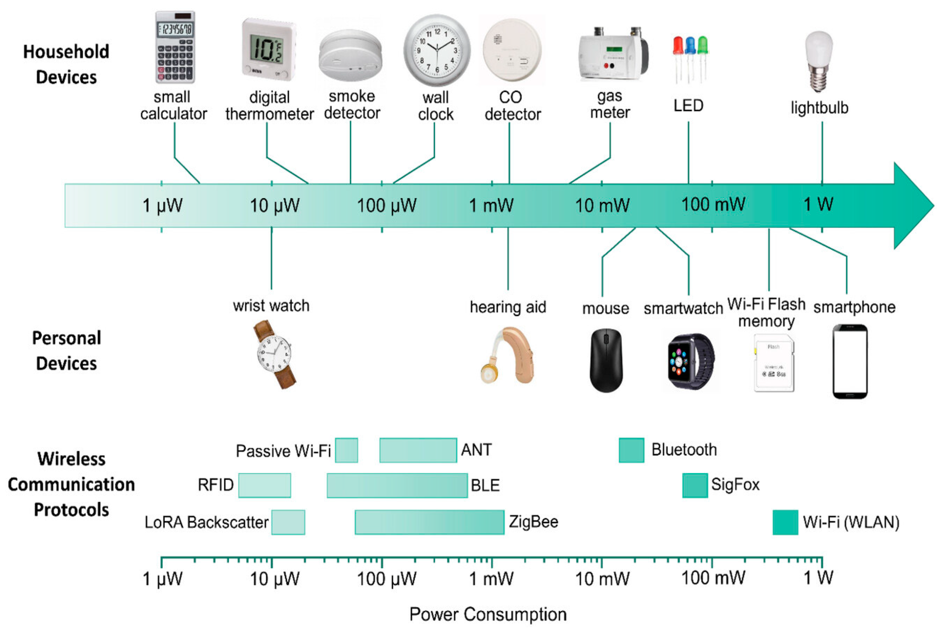
The IoT system refers to the automatic wireless connection between various electronic devices over the internet, i.e., the gathering and exchange of digital information in real time using electronic devices such as sensors, RFID, Bluetooth, and alarm systems. Indoor photovoltaics (IPVs) have huge potential to meet the power consumption demands for many tiny mobile platforms, including sensors, detectors, and consumer electronic devices. Hence, to power indoor IoT nodes, the EHS must deliver the required output power to drive the load. The power rating of IoT devices varies and depends on the application requirement [
34]. The nominal power consumption of home appliances, personal electronics, and wireless communication standards is between 1 μW and 1 W, as shown in
Figure 6.
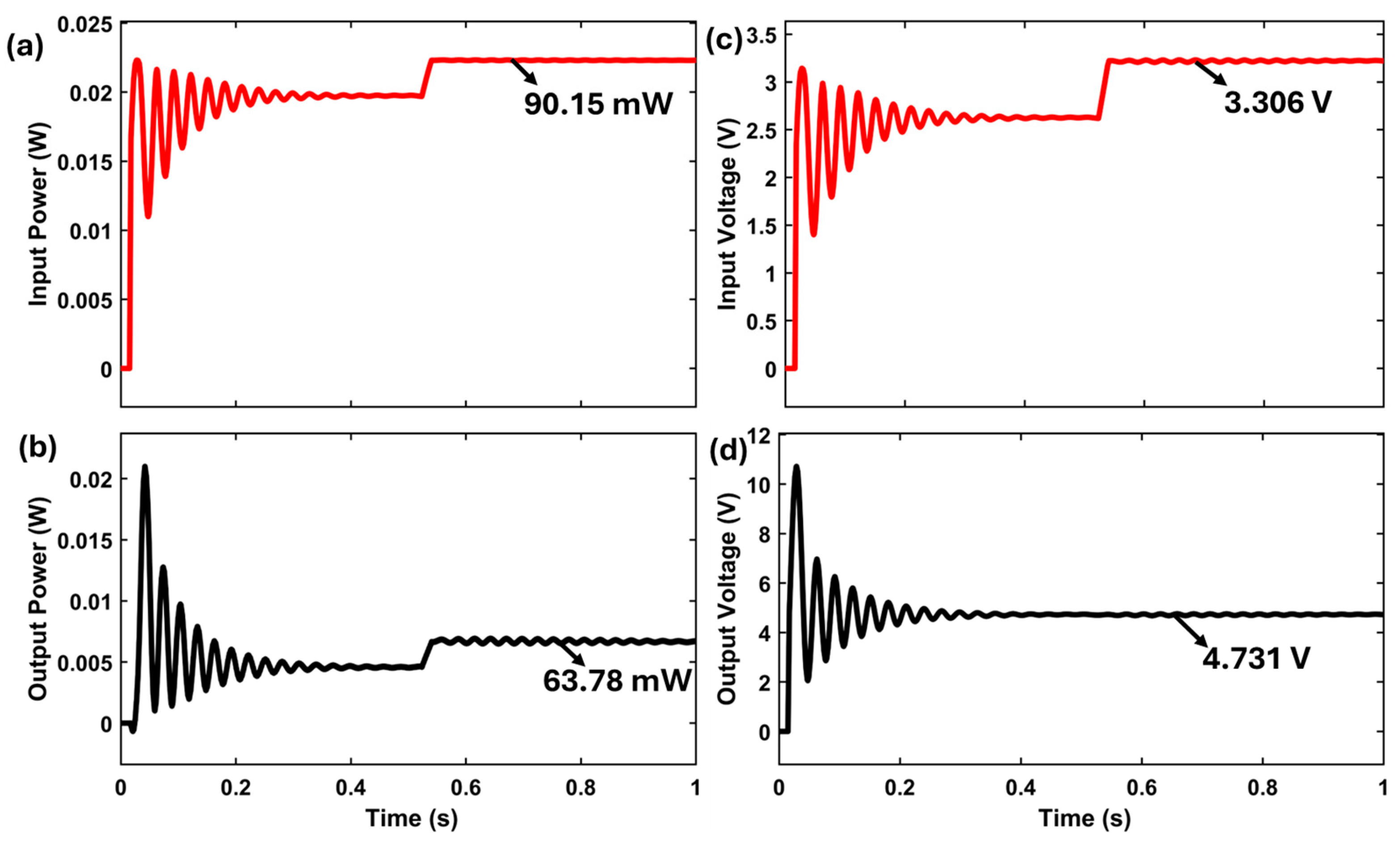
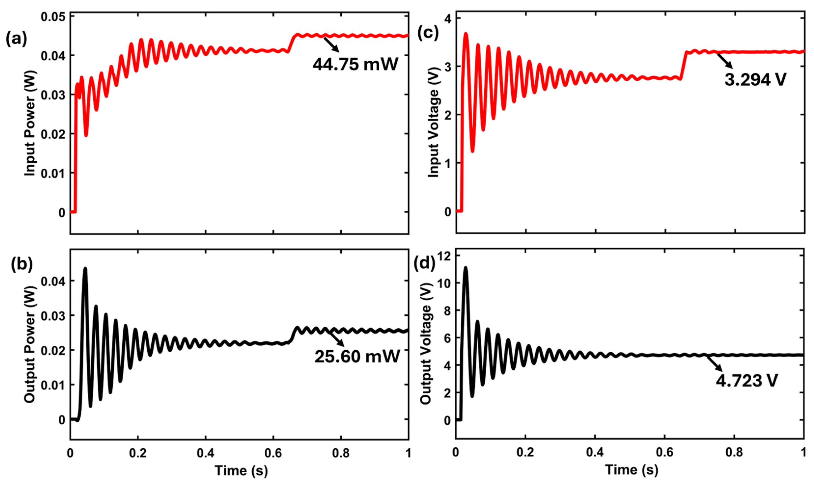
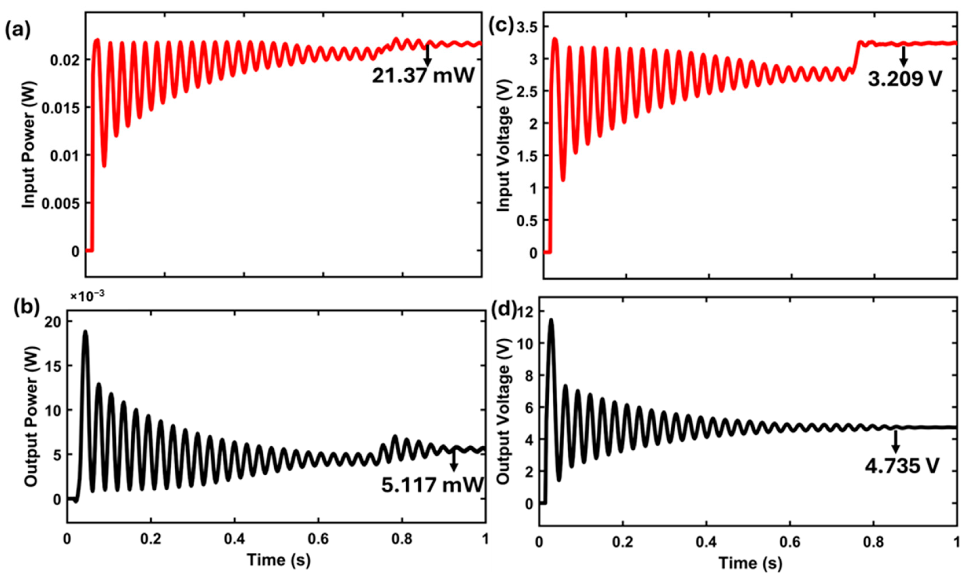
4. Discussion
Figure 9,
Figure 10, and
Figure 11 illustrate the input and output powers as well as input and output voltages at irradiance values of 200, 100, and 50 W/m
2, respectively. Fluctuations in
Figure 9,
Figure 10 and
Figure 11 are caused by the P&O algorithm. As irradiance decreases, the fluctuations in signals remain for a longer time. The system has worse performance for 50 W/m
2 as PSCs generate several times less current compared to the case with 200 W/m
2. Thus, the DC-DC converter undergoes a deviation in performance as the irradiance is changed. These fluctuations can be reduced by using another MPPT approach, such as the incremental conductance algorithm, which is more precise in MPP tracking and can quickly adapt to rapidly changed irradiance. However, P&O is preferred due to its low cost, easy implementation, and computational efficiency, which are sufficient for IoT applications. Nevertheless, the drawbacks of the P&O MPPT algorithm are its slow dynamic response, the drift problem under changing irradiance, and steady-state oscillation around the maximum power point, which affects the proposed system’s power quality and efficiency. Hence, using up-to-date novel tracking techniques based on artificial intelligence and optimization techniques could address the drawbacks of the classical P&O MPPT technique.
Despite the fluctuations in the output signals, the MPPT tracking efficiency remained at more than 95%.
Table 7 contains the input and output voltage and power values extracted from a simulation. The converter’s efficiency is reduced as the irradiance level has decreased, from around 70.75% at 200 W/m
2 to less than 30% at 50 W/m
2. For the small irradiance condition, boost converters show low performance. Thus, it is recommended to use charge pumps or other converters suitable for very low irradiance.
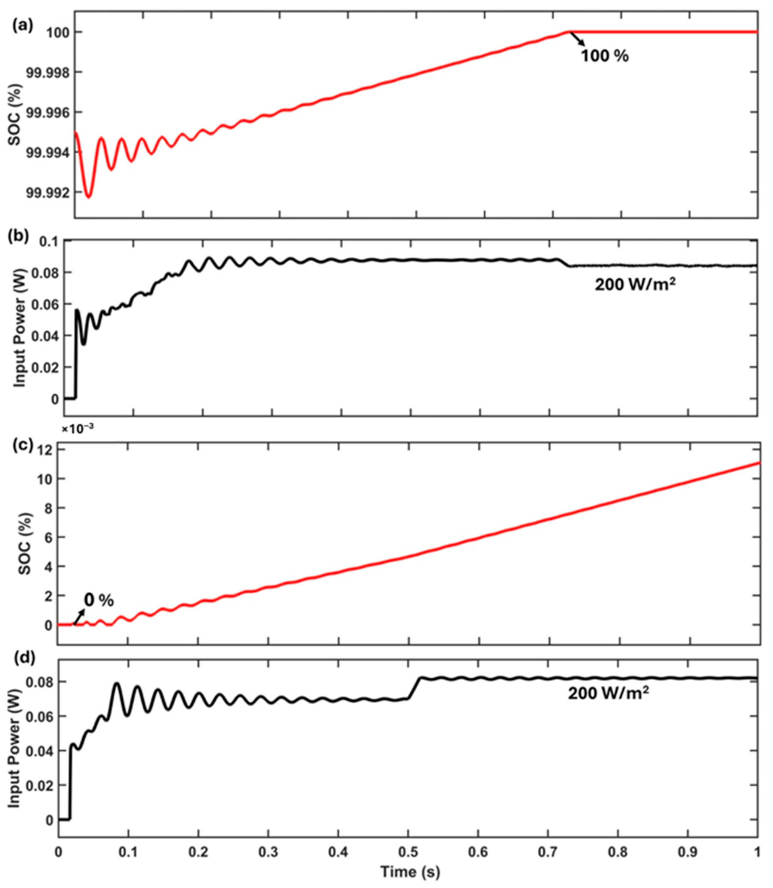
There are three additional cases in which simulations were conducted: for a fully charged battery (SOC 100%), a fully discharged battery (SOC 0%), and the incorporation of the IoT load profile. The EHS performance for fully charged and fully discharged batteries is illustrated in
Figure 12. The output resistor was removed so that PSC-generated energy was used to charge the battery at a faster rate than with the output resistor. In the real-world scenario, the system load is not a resistor and consumes a certain amount of power. Moreover, IoT applications tend to have power-saving modes when power consumption is very small. In
Figure 12a, the full battery charge is achieved at around 0.72 s, and it remains fully charged for the entire graph. The input power (
Figure 12b) was kept constant at 200 W/m
2 as the simulation used a resistive load (216.34 Ω). In the case of a deep battery discharge, an irradiance of 200 W/m
2 was set for the entire simulation. The SOC increased from 0 to ~0.011% in a 1 s simulation (
Figure 12c).
Tracking and converter efficiencies were calculated using Equations (5) and (6):
The third case that was simulated was the inclusion of the IoT load in the proposed EHS. The battery charge is kept at an SOC of 50%, and PSCs are subjected to an illumination of 200 W/m
2. The IoT load has power consumptions of 1.8, 12.3, and 94.2 mW for 3, 25, and 6.5 ms, respectively [
7]. The rest of the time, the IoT load consumes a 10 µA current. The simulated power profiles are plotted in
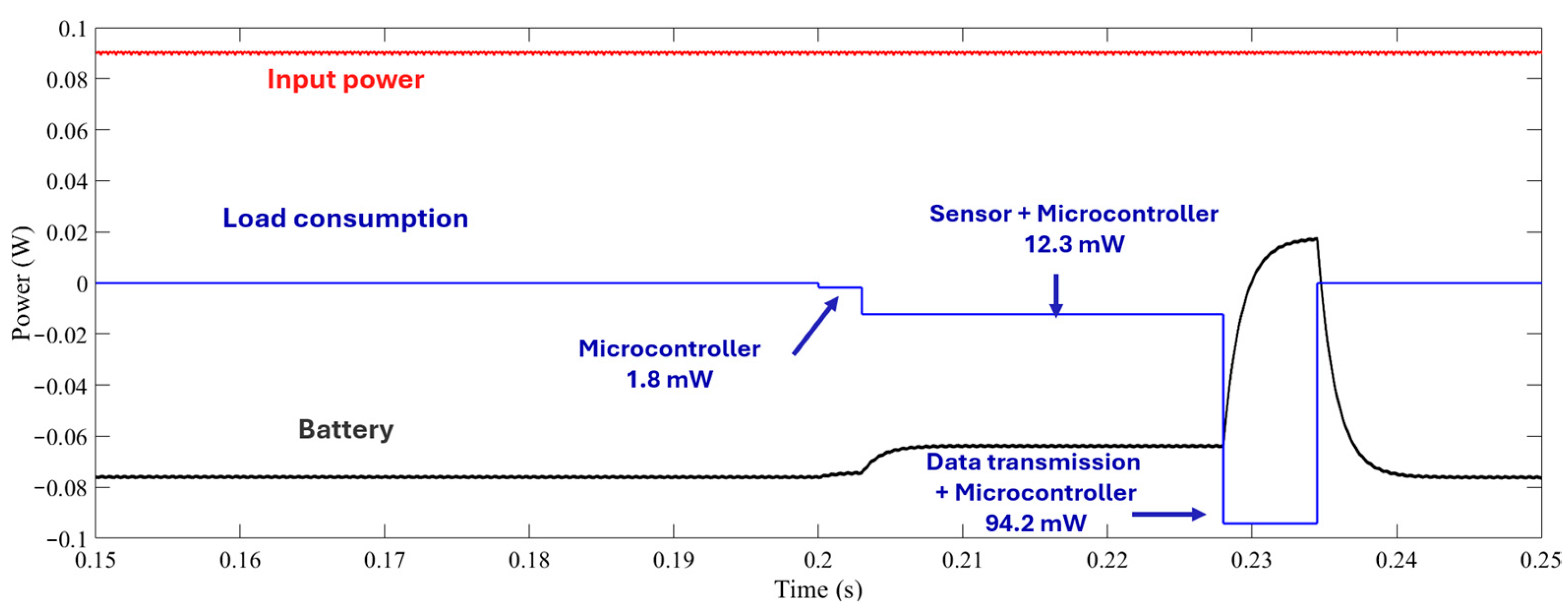
Figure 13. The excess input power from the PSCs is stored in the battery when the IoT load is small (up to 0.228 s and then starting again from 0.2345 s). The battery starts to discharge at around 0.23 s because the load consumption at that moment increases substantially from 12.3 mW to 94.2 mW. At a 200 W/m
2 illumination, the IoT load profile can operate frequently for every 30 s [
35]. At lower illumination levels, the load operation could be adjusted to a lower frequency to conserve energy, which, meanwhile, allows the PSCs to continuously charge the battery.
The findings of this study have significant implications for the future of energy harvesting and self-powered technology, especially in energy-autonomous IoT applications. The integration of PSCs within an optimized energy management system demonstrates a feasible approach to making IoT applications self-sufficient in indoor environments where conventional solar technologies are less suitable. This capability addresses the increasing demand for energy-efficient solutions in indoor conditions, which is common in smart homes, offices, and industrial environments. Real-world applications for such an approach may include sensors and other parts of smart homes and buildings, wearable devices, industrial IoT applications, and environmental monitoring. The modular design of the proposed EHS allows for its easy adaptation to different scales of operation, starting from low-power applications to larger smart home systems.
5. Conclusions
A PSC-powered EHS was successfully modeled using extracted I-V data from the experimentally fabricated PSC. The modeled PSC module was used to design and simulate an MPPT control system based on a DC-DC boost converter for an energy harvesting application. The P&O MPPT method was chosen owing to its straightforwardness, ease of implementation, and high tracking efficiency. The DC-DC boost converter increases the input voltage to a charging voltage of 4.2 V for the battery storage system, while the DC-DC buck–boost bidirectional converter and PI controllers regulate the charging and discharging rate of the battery system by operating in both buck mode and boost mode, and they consist of two diodes connected in anti-parallel with two switches. The PSC output power point is approximately 21.37 mW and 90.15 mW at the MPP, with an approximate efficiency of >95% at an irradiance of 50 W/m2 and 200 W/m2, respectively, while the range of the converter’s output power is between 5.117 mW and 63.78 mW. The power performance demonstrated in this work, along with the consideration of an IoT load profile used in the proposed EHS, indicates the potential of PSCs for indoor IoT applications. The power levels achieved would be sufficient to drive sensors, Bluetooth low-energy modules, low-power Wi-Fi networks, etc., which typically consume milliwatts of power. As the PCE of PSCs continues to rise with ongoing research and the development of efficient energy harvesting and management techniques, designs like the one presented in this study facilitate the realization of the autonomous operation of various wireless IoT applications indoors without reliance on fixed power sources or frequent battery replacement. This work, leveraging advances in PSC technology and focusing on efficient energy management via electronic engineering, contributes to ongoing research into creating sustainable power solutions for the rapidly expanding IoT field.


 ,
, 


