Abstract
This study presents an innovative method for the synthesis of indium aluminum nitride (InAlN) layers by direct current (DC) co-sputtering at room temperature, with the aim of reducing production costs of optoelectronic devices. Indium and aluminum targets are used, varying the power applied to the aluminum target. The results show that increasing the target power favors the formation of aluminum nitride (AlN), which modifies the chemical composition of the material. The layers obtained present smooth surfaces with a roughness of less than 3 nm, which is beneficial for applications requiring interfaces with low defect density. Regarding the optical properties, it is observed that the optical bandgap varies between 1.8 eV and 2.0 eV, increasing with the target power. Hall effect measurements indicate a decrease in the free carrier concentration and an increase in the resistivity with increasing power. This approach allows for the synthesis of InAlN with properties suitable for optoelectronic applications, solar cells, photocatalysis, and photoelectrocatalysis at low cost.
1. Introduction
Indium aluminum nitride (InAlN) has emerged as a promising semiconductor material, standing out because of its tunable direct bandgap between 0.64 eV and 6.2 eV depending on its stoichiometric composition [1,2,3]. This feature, together with its remarkable radiation resistance [4] and exceptional chemical stability, positions InAlN as an ideal candidate for the fabrication of high-efficiency solar cells [5] as well as for photocatalysis and photoelectrocatalysis. However, the synthesis of high-quality InAlN layers represents a significant challenge when seeking to reduce costs through room temperature fabrication processes [6].
The traditional synthesis of InAlN by sputtering requires temperatures above 200 °C to facilitate the reaction among nitrogen, indium, and aluminum atoms, thus promoting the formation of the compound [7,8]. These thermal conditions not only favor atomic mobility on the substrate, improving nucleation and, thus, the crystalline structure of the resulting layer, but are also crucial to avoid the formation of polycrystalline or amorphous structures [3]. In addition, these low-structural-quality layers usually exhibit a higher amount of electron–hole pair recombination centers, an attribute which is detrimental for the efficiency of a solar cell.
To date, the scientific literature has not reported on the synthesis of InAlN films with a wurzite-type crystal structure and a preferential c-plane orientation fabricated at room temperature. Therefore, the development of a method that allows for the synthesis of InAlN layers at room temperature, maintaining optimal properties for applications in optoelectronic devices, may represent a significant advance toward the reduction of production costs.
Additionally, the choice of sputtering type, either RF (radio frequency) or DC (direct current), plays a crucial role in the quality of the synthesized InAlN. Traditionally, RF sputtering has been preferred for the fabrication of InAlN [6,9,10] due to its ability to prevent charge accumulation on the indium target, thus facilitating the deposition of layers with high indium concentration. In contrast, DC sputtering, despite being more economical, faces significant challenges, such as the difficulty associated with maintaining a high indium concentration in the layers due to arcing, process disruption, and nonuniform target wear.
In this context, our research focuses on overcoming these challenges by developing a method using a DC co-sputtering system for the fabrication of InAlN layers at room temperature. This approach represents a step forward in the reduction of the costs associated with their production, thus opening new possibilities for the implementation of more affordable and efficient solar technologies, photocatalysis, and photoelectrocatalysis.
2. Materials and Methods
The InAlN films were deposited through a DC magnetron sputtering process. For this purpose, indium (99.99% purity) and aluminum (99.999% purity) targets, both 2 inches in diameter, were used. Argon and nitrogen gases were used as inert and reagent gases, respectively. The separation between the target and the substrate was 8 cm. The gas ratio was Ar:N2 = 2:8 sccm, with a base pressure of 1 × 10⁻⁷ Torr and an operating pressure of 10 mTorr. The substrate temperature was maintained at room temperature, with a total deposition time of 10 min. Different powers were experimented with for the aluminum target, specifically 60 W, 100 W, 140 W, and 180 W, while the power for the indium target was kept constant at 20 W. Glass substrates with a thickness of 1.1 ± 0.1 mm were used and ultrasonically cleaned in isopropyl alcohol and, subsequently, washed with deionized water.
Figure 1 illustrates the schematic of the growth system and the in situ chemical characterization system by X-ray photoelectron spectroscopy (XPS) and Auger electron spectroscopy (AES), using an AES-XPS system with an Al Kα (1486.6 eV) radiation source. The system includes an initial section isolated from the main chamber, designed to introduce the substrate without compromising the high vacuum of the main chamber and to allow the vacuum to be reached quickly. Once the sample is introduced and the vacuum is achieved, a valve is opened that allows the substrate to be moved into the coating chamber, where thin InAlN layers are deposited under vacuum conditions that can reach 10−8 Torr. After completion of the deposition, another valve allows the sample to be moved into the analysis chamber for chemical characterization by XPS. This in situ characterization is advantageous, as it allows the samples to be analyzed in their purest state, minimizing the presence of impurities such as carbon or oxygen atoms, and eliminates the need to calibrate the binding energies with respect to carbon for XPS analysis.
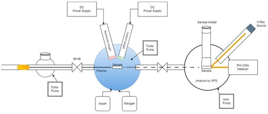
Figure 1.
Schematic of the synthesis equipment and characterization stage [11].
To determine the electrical properties of the layers, Hall effect measurements were performed using an ECOPIA HMS-5000 system with a Van der Pauw configuration. Additionally, ultraviolet–visible spectroscopy (UV–Vis) was used to determine the absorption coefficient of the layers and compare it with other semiconducting materials. The morphological properties of the layers were investigated by atomic force microscopy (AFM).
3. Results and Discussion
3.1. Chemical Properties
3.1.1. Auger Electron Spectroscopy (AES)
The analysis of the AES spectrum in Figure 2 confirms that all samples showed the characteristic peaks of indium (In), nitrogen (N), oxygen (O), and carbon (C) atoms. Specifically, the indium peak was detected at 408 eV, corresponding to the MNN transition where an electron is ejected from the M subshell and an electron from the N subshell fills the gap, while another electron from the N subshell is emitted as an Auger electron. The nitrogen peak was observed at 386 eV, associated with the KLL transition [12] which entails a process similar to that of the MNN transition: an electron is ejected from the K subshell and an electron from the L subshell fills the gap, emitting another electron from the L subshell as an Auger electron. The expected aluminum peak at 1396 eV for the LMM transition was not detected within the measurement range used. In addition, small peaks for oxygen (513 eV) and carbon (292 eV) were observed, indicative of slight contamination in the deposition chamber. A peak at 366 eV was also observed, suggesting the presence of chemical effects related to the covalent bond between indium and nitrogen, confirming the formation of InN. Binary InN is estimated to be stoichiometric from the height ratios of the In/N peaks in the spectrum.
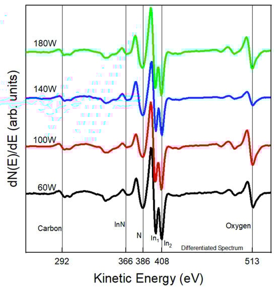
Figure 2.
AES spectrum of InAlN films: identification of elements and evidence of InN formation.
3.1.2. X-ray Photoelectron Spectroscopy (XPS)
To complement the chemical analysis, the survey spectrum in Figure 3 obtained by XPS reveals the presence of four chemical elements: oxygen (O), indium (In), nitrogen (N), and aluminum (Al). The peaks identified in the survey spectrum corresponded to the binding energies O1s at 531.4 eV, In3d5/2 at 444.5 eV, N1s at 396.6 eV, and Al-2p at 73.7 eV [13,14]. It is important to highlight that, through this XPS analysis, it was possible to identify aluminum atoms in the samples, a result that had not been possible by means of the previously used AES. The carbon peak was not identified in the XPS spectrum because the fabrication was performed under high vacuum and the characterization by XPS was carried out in situ under ultra-high vacuum conditions.
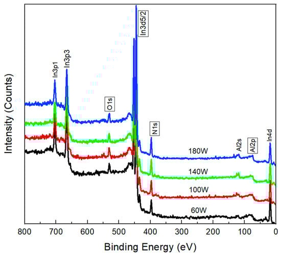
Figure 3.
XPS spectra of InAlN layers. Identification of oxygen, indium, nitrogen, and aluminum.
Figure 4 illustrates the high-resolution spectra corresponding to the Al-2p, In3d5/2, and N1s peaks of the samples fabricated under various deposition powers. From the spectral data, an increase in the intensity of the Al-2p and N1s peaks was observed with increasing power applied to the target. This phenomenon suggests an increased incorporation of aluminum and nitrogen into the film, a phenomenon which is consistent with the formation of aluminum nitride (AlN), evidenced by the increase in the N1s peak. On the other hand, the intensity of the In3d5/2 peak decreased, indicating a reduction in indium concentration in the films as the power increased. These results point to a modification in the chemical composition of the films, favoring the formation of AlN to the detriment of indium incorporation.
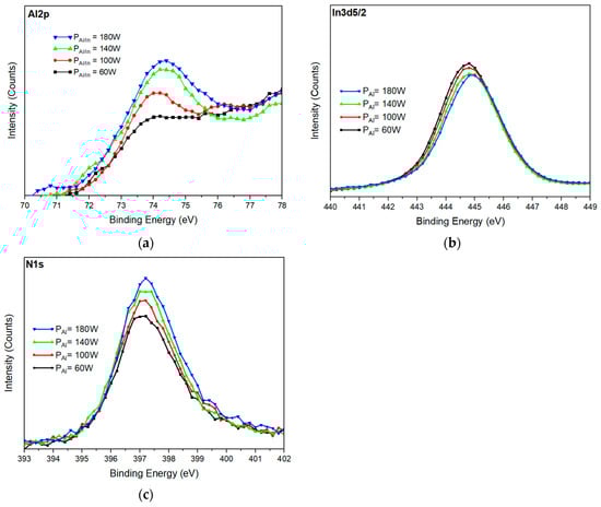
Figure 4.
Variation of high-resolution spectra of (a) Al-2p, (b) In3d5/2, and (c) N1s peaks as a function of target power.
Mathematical deconvolution of the high-resolution XPS spectra for the N1s, Al-2p, and In3d5/2 peaks was performed to determine the chemical nature of the bonds present in the samples. This deconvolution employed Gaussian functions and Shirley-type baseline fits. The results are presented in Figure 5, which illustrates the deconvolution for samples prepared at different deposition strengths.
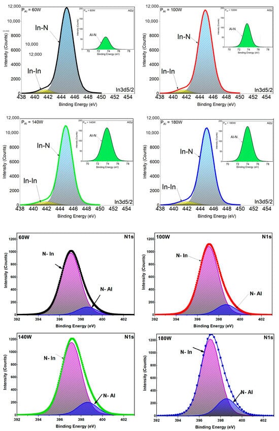
Figure 5.
Deconvolution of the XPS spectra of the In3d5/2, Al-2p, and N1s peaks.
Figure 5 presents the deconvolution of the In3d5/2 peak for each sample into two main subpeaks, centered at 444.81 eV and 441.9 eV, corresponding to the In–N and In–In bonds, respectively. The presence of the In–N bond confirms indium nitridation; however, the In–In subpeak suggests incomplete nitridation, evidencing slight indium segregation. The insets show the Al-2p core level Al-2p spectra, fitted by a Gaussian curve centered at 73.97 eV, assigned to the Al–N bonds. Deconvolution of the Al-2p peak revealed no Al–Al bonds, ruling out aluminum segregation. This indicates the successful formation of the In–N and Al–N bonds, thus demonstrating the effective formation of the InAlN alloy.
In the spectra of the N1s peak (Figure 5), two subpeaks are clearly identifiable, corresponding to the N–In and N–Al bonds, with binding energies of 396.4 eV and 399.2 eV, respectively [15,16,17]. Detailed deconvolution analysis indicates that, with increasing target power, the subpeak corresponding to N–Al increased in intensity, while the N–In subpeak decreased. This behavior suggests an increased formation of AlN and a reduction in the presence of InN within the semiconducting material.
Quantification of the ratio of N–In and N–Al bonds was performed by deconvolution of the N1s peak in the XPS spectra of each sample. This analysis allowed us to determine the stoichiometry of the samples and examine how this varies as a function of the power applied to the aluminum target. The results of this study are summarized in Table 1, which shows the evolution of the chemical formula of InAlN with power variation. A 6% variation in stoichiometry was observed, which is a good result considering that it is a DC co-sputtering process at room temperature.

Table 1.
Changes in the chemical composition of InAlN in relation to the applied power.
The deconvolution of the In3d5/2 peaks is presented in the inset in each high-resolution spectrum of the N1s peak for each sample. This deconvolution revealed the presence of two types of bonds: In–In and In–N. The area under the In–In peak was considerably smaller compared to the area under the In–N peak, indicating that nitridation was almost completely carried out.
Figure 6 shows a comparative analysis of how the power applied to the aluminum target affected the InAlN stoichiometry using a DC co-sputtering at room temperature and holding the indium target power constant. This study is compared with previous research which used RF co-sputtering at temperatures above 300 °C, where the indium target power was also held fixed. The results indicate that the use of a room temperature DC system is feasible and allows the stoichiometry of InAlN to be effectively modified. This method significantly reduces fabrication costs, which is crucial for the mass production of optoelectronic devices.
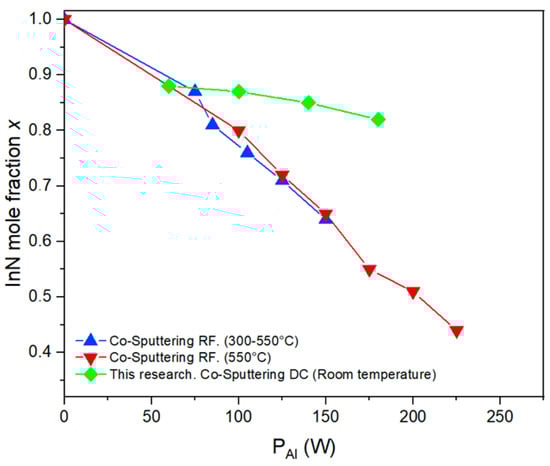
Figure 6.
Variation of InN and AlN mole fractions with target power [6,18].
3.2. Morphological Properties
Atomic Force Microscopy (AFM)
Morphological properties were analyzed by atomic force microscopy (AFM). This morphological analysis provided quantitative data, as shown in Table 2. In this table, it is observed that, as the aluminum target power increased, the thickness of the layer increased and, thus, its deposition rate.
Table 2.
Variation in InAlN thickness and deposition rate as a function of aluminum blank power.
A surface area of 4 μm2 was analyzed on each sample to obtain a detailed representation of its morphology. In Figure 7, 3D images obtained by AFM are presented. These images revealed very smooth surface textures, which is a characteristic of the sputtering technique.
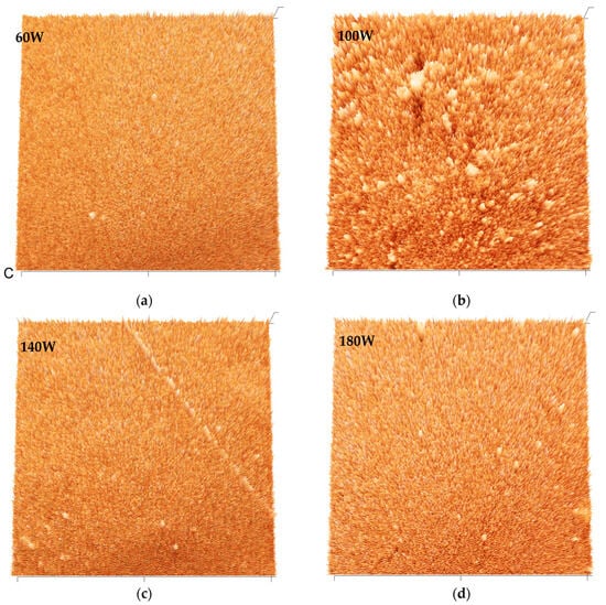
Figure 7.
3D AFM images of InAlN layers fabricated at different sputtering powers: (a) 60 W, (b) 100 W, (c) 140 W, and (d) 180 W. The scale is 2 µm × 2 µm × 15 nm.
From the statistical analysis of the previous images, Figure 8a was produced, which illustrates the root mean square (RMS) roughness of the samples as a function of the power applied to the aluminum target. This RMS measure reflects the standard deviation of the height distribution of the analyzed surfaces. In general terms, the samples exhibited exceptionally smooth surfaces, with roughness values below 3 nm. There was a tendency where, as the aluminum target power increased, the RMS roughness tended to decrease. Something interesting in this research is that very low roughness values were obtained compared to other samples. As observed in Figure 8b [1,3,9,13,16,19], a low roughness is desirable for the fabrication of interfaces with low defect density [20], which is useful for the improvement of high-efficiency solar cells.
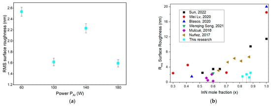
Figure 8.
(a) Roughness of InAlN surfaces obtained at different sputtering powers; (b) roughness obtained for different InAlN stoichiometries across different investigations [3,6,8,9,13,16].
To analyze the peak height distribution of the samples, a threshold was used to differentiate the grains from the background by classifying points above the threshold as grains and the rest as background. Figure 9 shows the peak height distribution plot on the surfaces of the samples obtained at different sputtering powers.
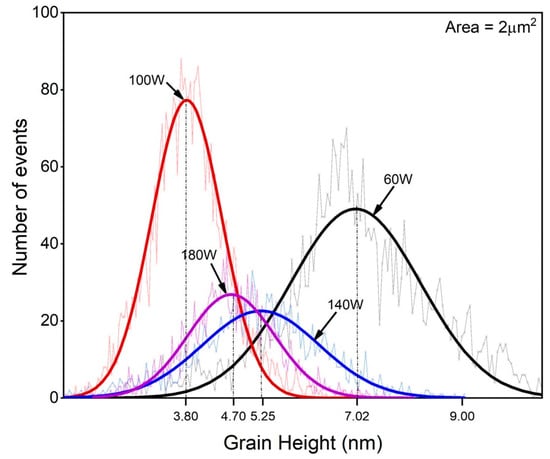
Figure 9.
Influence of sputtering power on the morphology of InAlN surfaces.
In the analysis of the height distribution, variations in the predominant height were observed as a function of the applied power. Specifically, at 60 W, the predominant height was 7.02 nm; as the power was increased to 100 W, it decreased to 3.80 nm. At 140 W, it increased again to 5.25 nm, and, at 180 W, it reached 4.70 nm. These results suggest that there was no direct relationship between the prevailing height and the power applied to the aluminum target.
However, when calculating the area under the Gaussian curves, a high dependence of the area on the applied power was evident, indicating that the power influenced the number of peaks present in the samples. The peak area was inversely proportional to the applied power. Consequently, the sample fabricated at 180 W exhibited the smallest area, followed by those fabricated at 140 W and 100 W, while the sample fabricated at 60 W exhibited the largest area. This is beneficial in applications where high surface quality is required, such as in optoelectronic devices or high mobility transistors (HEMTs) where surfaces with lower trap density are required.
3.3. Optical Properties
Ultraviolet–Visible Spectroscopy (UV–Vis)
The optical properties of the semiconductor layers with various stoichiometries were analyzed using UV–Vis. In this study, the optical transmittance of the samples was evaluated over a range of energies from 1.5 eV to 4.0 eV, spanning both the visible and ultraviolet spectra. The results of these measurements are presented in Figure 10. The figure shows that the samples exhibited a high transmittance in the near infrared. However, this transmittance decreased progressively in the visible spectrum, from the red to the violet. Furthermore, it is highlighted that an increase in target power, leading to a higher proportion of AlN in the sample, resulted in an increase in transmittance.
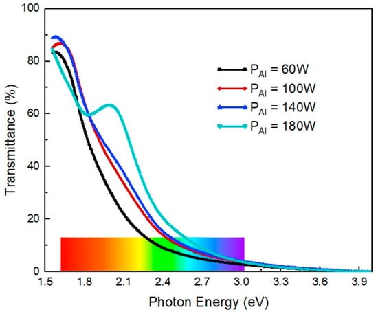
Figure 10.
Optical transmittance of InAlN layers as a function of target power.
The oscillation observed in the 180 W sample in the transmittance plot in Figure 4 was due to light interference as it struck a thin film. The reflected waves on the top and bottom surfaces of the film interfered with each other, creating oscillation patterns. This interference was influenced by film thickness and photon energy. The greater thickness of the 180 W film increased the probability of interference at low energies, as it absorbed less energy and allowed internal reflection of the light, generating the observed oscillation. The other samples did not have adequate absorbance or thickness to produce significant interference, possibly because the additional optical path needed for constructive or destructive interference was not achieved at these thicknesses.
Figure 11 illustrates the absorption coefficient of the samples as a function of photon energy. It is observed that the absorption coefficient was highest in the sample fabricated at the lowest target power and decreased as the power increased. This behavior suggests that the absorption of light by the semiconductor material decreased with increasing AlN content.
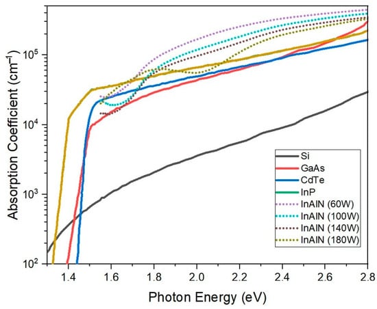
Figure 11.
Variation of absorption coefficient with photon energy as a function of target power in InAlN layers [21].
To determine the bandgap of the samples, the Tauc method was used, which involves plotting (αhν)2 as a function of photon energy, where α represents the absorption coefficient and hν the photon energy [22,23]. Figure 12 displays the results obtained, showing that the bandgap ranged between 1.8 eV and 2.0 eV as the power of the aluminum target was varied. These values lie within the visible spectrum, specifically in the red–orange range. Furthermore, it was observed that the bandgap increased with increasing target power, which is consistent with theory [3].
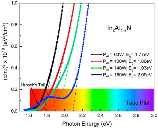
Figure 12.
Determination of the bandgap of InAlN layers by the Tauc method and its variation with target power.
The bandgap values obtained are comparable with those of materials such as CdTe (1.48 eV) and CdS (2.4 eV) [24,25], commonly used as absorber layer and window layer, respectively, in solar cells. This suggests that the InAlN alloy fabricated at room temperature by DC sputtering could be used in solar cells, photocatalysis, and photoelectrocatalysis [26,27].
The explanation for these bandgap values can be found in the high working pressure of 10 mTorr used during the deposition process which reduced the kinetic energy of the incident atoms on the substrate and complicated the formation of a more ordered crystalline structure, thus increasing the optical bandgap of the material. Figure 12 also highlights the presence of the Urbach tail in all samples, attributable to disordered potentials [2]. However, the sample fabricated at 180 W showed a particular shape of this tail, attributable to the distribution of available states within the bandgap, originated by structural defects.
3.4. Electrical Properties
Hall Effect
The concentration of free carriers (n) in the InAlN layers was determined using the Hall effect method. Figure 13 illustrates how n varied as a function of the power applied to the aluminum target. It was observed that n decreased as the power increased, reflecting a reduction in the number of carriers in the conduction band. This trend is explained by the fact that increasing the power decreased the indium (In) content in the InAlN layers. This decrease in the carrier concentration is attributed to the decrease in Fermi energy with respect to the conduction band edge [28].
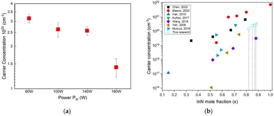
Figure 13.
Variation of free carrier concentration in InAlN layers with target power. (a) This research, (b) comparison with other reports [3,6,8,9,13,16].
The obtained values of n ranged from 3.1 × 10²⁰ to 1.5 × 10²⁰, figures that, although high, are within the range reported in the literature for this type of semiconductors fabricated through sputtering [1,3,9,13,16,19]. The high carrier concentration can be attributed to the presence of impurities and donor defects in the material. In addition, the use of glass as a substrate contributed to the generation of these defects, influencing the observed free carrier concentration [5,29].
Figure 14 illustrates how the resistivity of the InAlN layers varied as a function of the power applied to the aluminum target. An increase in resistivity was observed as the power increased, reflecting a decrease in the electrical conductivity of the material. This behavior is attributable to the intrinsic properties of AlN, which is more resistive compared to InN. As a result, the electrons in the material were more confined, a phenomenon which reduced their mobility and, thus, the electrical conductivity of the semiconductor.
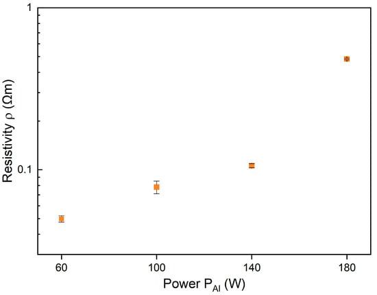
Figure 14.
Increase in resistivity in InAlN layers with an increase in aluminum target power.
Figure 15 shows how the free carrier mobility (μ) varied as a function of the power applied to the aluminum target. It was observed that μ decreased with increasing power, indicating that the electrons found it more difficult to move inside the material. The μ values obtained ranged from 14.01 cm2/Vs to 0.16 cm2/Vs, figures that, although low, are within the range reported in the literature for InAlN [30]. One of the factors affecting carrier mobility is the high dispersion of peak heights on the surface, a phenomenon which increases roughness and reduces free movement.
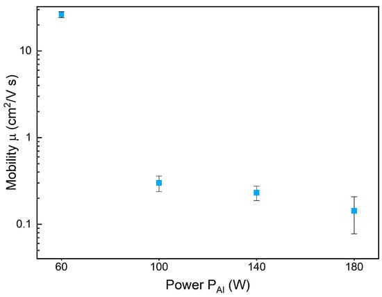
Figure 15.
Decrease in InAlN mobility with target power.
4. Conclusions
This research presents significant advances in the synthesis of indium aluminum nitride (InAlN) layers by DC co-sputtering at room temperature, a process which represents a significant advance in the reduction of production costs for optoelectronic devices. It is demonstrated that, by increasing the power applied to the aluminum target, the formation of aluminum nitride (AlN) is favored, a phenomenon which modifies the chemical composition of the material and allows for the adjustment of its optical and electrical properties. The layers obtained present exceptionally smooth surfaces, with roughness of less than 3 nm, an attribute which is ideal for applications requiring interfaces. In optical terms, the bandgap is observed to vary between 1.8 eV and 2.0 eV, increasing with target power and suggesting its potential use in solar cells. Hall effect measurements reveal a decrease in free carrier concentration and an increase in resistivity with increasing power, reflecting lower electrical conductivity. These results indicate that the developed method is not only feasible for large-scale production of cheaper optoelectronic devices, but also allows for the maintenance of suitable properties for their performance. This innovative approach could facilitate the implementation of more affordable and efficient solar technologies, thus contributing to technological progress in the semiconductor field.
Author Contributions
Conceptualization, L.F.M.-N.; methodology, J.D.C.-B.; software, J.D.C.-B.; formal analysis, L.F.M.-N. and J.D.C.-B.; writing—original draft preparation, J.D.C.-B.; writing—review and editing, L.F.M.-N.; supervision, L.F.M.-N. All authors have read and agreed to the published version of the manuscript.
Funding
This research was funded by MINCIENCIAS, Ph.D. Grant.
Data Availability Statement
The datasets presented in this article are not readily available.
Conflicts of Interest
The authors declare no conflicts of interest. The funders had no role in the design of the study, in the collection, analyses, or interpretation of the data, in the writing of the manuscript, or in the decision to publish the results.
References
- Lv, W.; Shen, L.; Liu, J.; Chen, J.; Wu, L.; Qi, D.; Zhang, G.; Li, X. Mechanical properties of single-phase Al1−xInxN films across the compositional range (0 ≤ x ≤ 0.7) grown by radio-frequency magnetron sputtering. Appl. Surf. Sci. 2020, 504, 144335. [Google Scholar] [CrossRef]
- He, H.; Cao, Y.; Fu, R.; Guo, W.; Huang, Z.; Wang, M.; Huang, C.; Huang, J.; Wang, H. Band gap energy and bowing parameter of In-rich InAlN films grown by magnetron sputtering. Appl. Surf. Sci. 2010, 256, 1812–1816. [Google Scholar] [CrossRef]
- Blasco, R.; Valdueza-Felip, S.; Montero, D.; Sun, M.; Olea, J.; Naranjo, F.B. Low-to-Mid Al Content (x = 0–0.56) AlxIn1−xN Layers Deposited on Si(100) by Radio-Frequency Sputtering. Phys. Status Solidi B Basic Res. 2020, 257, 1900575. [Google Scholar] [CrossRef]
- Smith, M.D.; O’mahony, D.; Vitobello, F.; Muschitiello, M.; Costantino, A.; Barnes, A.R.; Parbrook, P.J. A comparison of the 60 Co gamma radiation hardness, breakdown characteristics and the effect of SiN x capping on InAlN and AlGaN HEMTs for space applications. Semicond. Sci. Technol. 2015, 31, 025008. [Google Scholar] [CrossRef]
- Mulcué-Nieto, L.F.; Saldarriaga, W.; de la Cruz, W.; Restrepo, E.; Ospina, M.S.; Escobar, D. Study of InAlN thin films deposited on silicon, ITO/PET, and ITO/GLASS substrates at room temperature for its possible use in solar cells. J. Mater. Sci. Mater. Electron. 2022, 33, 1162–1172. [Google Scholar] [CrossRef]
- Núñez-Cascajero, A.; Valdueza-Felip, S.; Monteagudo-Lerma, L.; Monroy, E.; Taylor-Shaw, E.; Martin, R.; Gonzalez-Herraez, M.; Naranjo, F.B. In-rich AlxIn1-xN grown by RF-sputtering on sapphire: From closely-packed columnar to high-surface quality compact layers. J. Phys. D Appl. Phys. 2017, 50, 065101. [Google Scholar] [CrossRef]
- Peng, T.; Piprek, J.; Qiu, G.; Olowolafe, J.O.; Unruh, K.M. Band gap bowing and refractive index spectra of polycrystalline AlxIn1−xN films deposited by sputtering. Appl. Phys. Lett. 1997, 71, 2439–2441. [Google Scholar] [CrossRef]
- Dong, C.; Xu, M.; Chen, Q.; Liu, F.; Zhou, H.; Wei, Y.; Ji, H. Growth of well-oriented AlxIn1−x N films by sputtering at low temperature. J. Alloys Compd. 2009, 479, 812–815. [Google Scholar] [CrossRef]
- Sun, M.; Blasco, R.; Nwodo, J.; de la Mata, M.; Molina, S.I.; Ajay, A.; Monroy, E.; Valdueza-Felip, S.; Naranjo, F.B. Comparison of the Material Quality of AlxIn1−xN (x—0–0.50) Films Deposited on Si(100) and Si(111) at Low Temperature by Reactive RF Sputtering. Materials 2022, 15, 7373. [Google Scholar] [CrossRef]
- Liu, H.F.; Tan, C.C.; Dalapati, G.K.; Chi, D.Z. Magnetron-sputter deposition of high-indium-content n-AlInN thin film on p-Si(001) substrate for photovoltaic applications. J. Appl. Phys. 2012, 112, 063114. [Google Scholar] [CrossRef]
- Garzon-Fontecha, A.; Castillo, H.A.; Curiel, M.; Montaño-Figueroa, A.G.; Quevedo-Lopez, M.A.; Cota-Araiza, L.; De La Cruz, W. SnOx thin films tunable conductivity for fabrication of p-n homo-junction. Surf. Interface Anal. 2020, 53, 68–75. [Google Scholar] [CrossRef]
- Guo, Q.; Tanaka, T.; Nishio, M.; Ogawa, H. Optical bandgap energy of wurtzite in-rich AllnN alloys. Jpn. J. Appl. Phys. Part 2 Lett. 2003, 42, L141–L143. [Google Scholar] [CrossRef]
- Song, W.; Li, T.; Zhang, L.; Zhu, W.; Wang, L. Influence of growth parameters on microstructures and electrical properties of InxAl1−xN thin films using sputtering. J. Alloys Compd. 2021, 885, 160977. [Google Scholar] [CrossRef]
- Miyoshi, M.; Kuraoka, Y.; Tanaka, M.; Egawa, T. Metalorganic chemical vapor deposition and material characterization of lattice-matched InAlN/GaN two-dimensional electron gas heterostructures. Appl. Phys. Express 2008, 1, 081102. [Google Scholar] [CrossRef]
- Alizadeh, M.; Ganesh, V.; Pandikumar, A.; Goh, B.; Azianty, S.; Huang, N.; Rahman, S. Photoelectrochemical behavior of AlxIn1-xN thin films grown by plasma-assisted dual source reactive evaporation. J. Alloys Compd. 2016, 670, 229–238. [Google Scholar] [CrossRef]
- Mulcué-Nieto, L.F.; Acosta-Medina, C.D.; Saldarriaga, W.; Mendoza, S. Structural, morphological, electrical and optical properties of amorphous InxAl1-xN thin films for photovoltaic applications. J. Non-Cryst. Solids 2018, 499, 328–336. [Google Scholar] [CrossRef]
- Taborda, J.A.P.; Caicedo, J.C.; Grisales, M.; Saldarriaga, W.; Riascos, H. Deposition pressure effect on chemical, morphological and optical properties of binary Al-nitrides. Opt. Laser Technol. 2015, 69, 92–103. [Google Scholar] [CrossRef]
- Valdueza-Felip, S.; Blasco, R.; Olea, J.; Díaz-Lobo, A.; Braña, A.F.; Naranjo, F.B. AlxIn1-xN on Si (100) Solar Cells (x = 0–0.56) deposited by RF sputtering. Materials 2020, 13, 2336. [Google Scholar] [CrossRef]
- Núñez-Cascajero, A.; Monteagudo-Lerma, L.; Valdueza-Felip, S.; Navío, C.; Monroy, E.; González-Herráez, M.; Naranjo, F.B. Study of high In-content AlInN deposition on p-Si(111) by RF-sputtering. Jpn. J. Appl. Phys. 2017, 55, 05FB07. [Google Scholar] [CrossRef]
- Perillat-merceroz, G.; Cosendey, G.; Carlin, J.; Butté, R.; Grandjean, N. Intrinsic degradation mechanism of nearly lattice-matched InAlN layers grown on GaN substrates Intrinsic degradation mechanism of nearly lattice-matched InAlN layers grown on GaN substrates. J. Appl. Phys. 2013, 113, 063506. [Google Scholar] [CrossRef]
- PVEducation.org. Absorption Coefficient. [Online]. Available online: https://www.pveducation.org/pvcdrom/pn-junctions/absorption-coefficient (accessed on 28 April 2024).
- Aschenbrenner, T.; Dartsch, H.; Kruse, C.; Anastasescu, M.; Stoica, M.; Gartner, M.; Pretorius, A.; Rosenauer, A.; Wagner, T.; Hommel, D. Optical and structural characterization of AlInN layers for optoelectronic applications. J. Appl. Phys. 2010, 108, 063533. [Google Scholar] [CrossRef]
- Chen, J.J.; Qi, D.L.; Li, X.F.; Song, J.Y.; Shen, L.H. Optical and electrical properties of Al1-xInxN films with a wide middle-composition range by RF sputtering. Appl. Phys. A Mater. Sci. Process. 2022, 128, 142. [Google Scholar] [CrossRef]
- Fonthal, G.; Tirado-Mejı, L.; Marı, J.I.; Ariza-Calderón, H.; Mendoza-Alvarez, J.G. Temperature dependence of the band gap energy of crystalline CdTe. J. Phys. Chem. Solids 2000, 61, 579–583. [Google Scholar] [CrossRef]
- Oliva, A.; Solıs-Canto, O.; Castro-Rodrıguez, R.; Quintana, P.; Mexicó, M. Formation of the band gap energy on CdS thin films growth by two different techniques. Thin Solid Films 2001, 391, 28–35. [Google Scholar] [CrossRef]
- Nakamura, K.; Kobayashi, A.; Ueno, K.; Ohta, J.; Fujioka, H. AlN/InAlN thin-film transistors fabricated on glass substrates at room temperature. Sci. Rep. 2019, 9, 6254. [Google Scholar] [CrossRef]
- Afzal, N.; Devarajan, M.; Ibrahim, K. A comparative study on the growth of InAlN films on different substrates. Mater. Sci. Semicond. Process. 2016, 51, 8–14. [Google Scholar] [CrossRef]
- Alizadeh, M.; Tong, G.B.; Mehmood, M.S.; Qader, K.W.; Rahman, S.A.; Shokri, B. Band engineered Al-rich InAlN thin films as a promising photoanode for hydrogen generation from solar water splitting. Sol. Energy Mater. Sol. Cells 2018, 185, 445–455. [Google Scholar] [CrossRef]
- Hsieh, P.-Y.; Wu, J.-Y.; Chang, T.-F.M.; Chen, C.-Y.; Sone, M.; Hsu, Y.-J. Near infrared-driven photoelectrochemical water splitting: Review and future prospects. Arab. J. Chem. 2020, 13, 8372–8387. [Google Scholar] [CrossRef]
- Mulcue, L.F.; de la Cruz, W.; Saldarriaga, W. Effect of film thickness on morphological, structural and electrical properties of InAlN thin layers grown on glass at room temperature. Appl. Phys. A 2021, 127, 479. [Google Scholar] [CrossRef]
Disclaimer/Publisher’s Note: The statements, opinions and data contained in all publications are solely those of the individual author(s) and contributor(s) and not of MDPI and/or the editor(s). MDPI and/or the editor(s) disclaim responsibility for any injury to people or property resulting from any ideas, methods, instructions or products referred to in the content. |
© 2024 by the authors. Licensee MDPI, Basel, Switzerland. This article is an open access article distributed under the terms and conditions of the Creative Commons Attribution (CC BY) license (https://creativecommons.org/licenses/by/4.0/).