
Design and Implementation of a DC–DC Resonant LLC Converter for Electric Vehicle Fast Chargers


Abstract
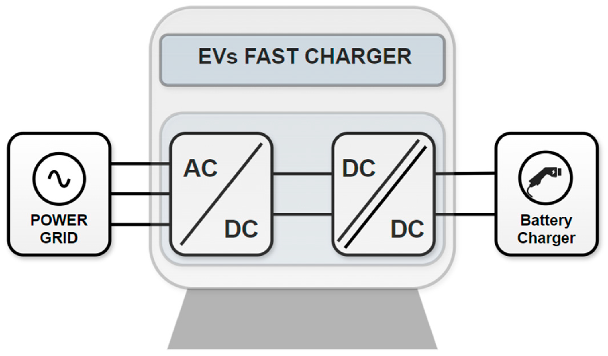
1. Introduction
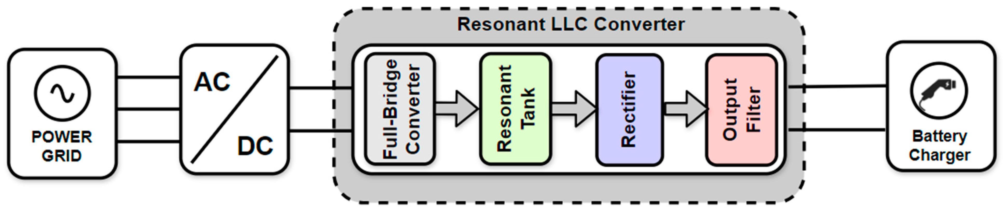
2. Design of the DC–DC LLC Resonant Converter
2.1. Design of the Isolated DC–DC LLC Resonant Converter
2.2. Advantages and Disadvantages of the Isolated DC–DC Resonant LLC Converter
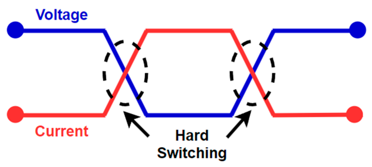
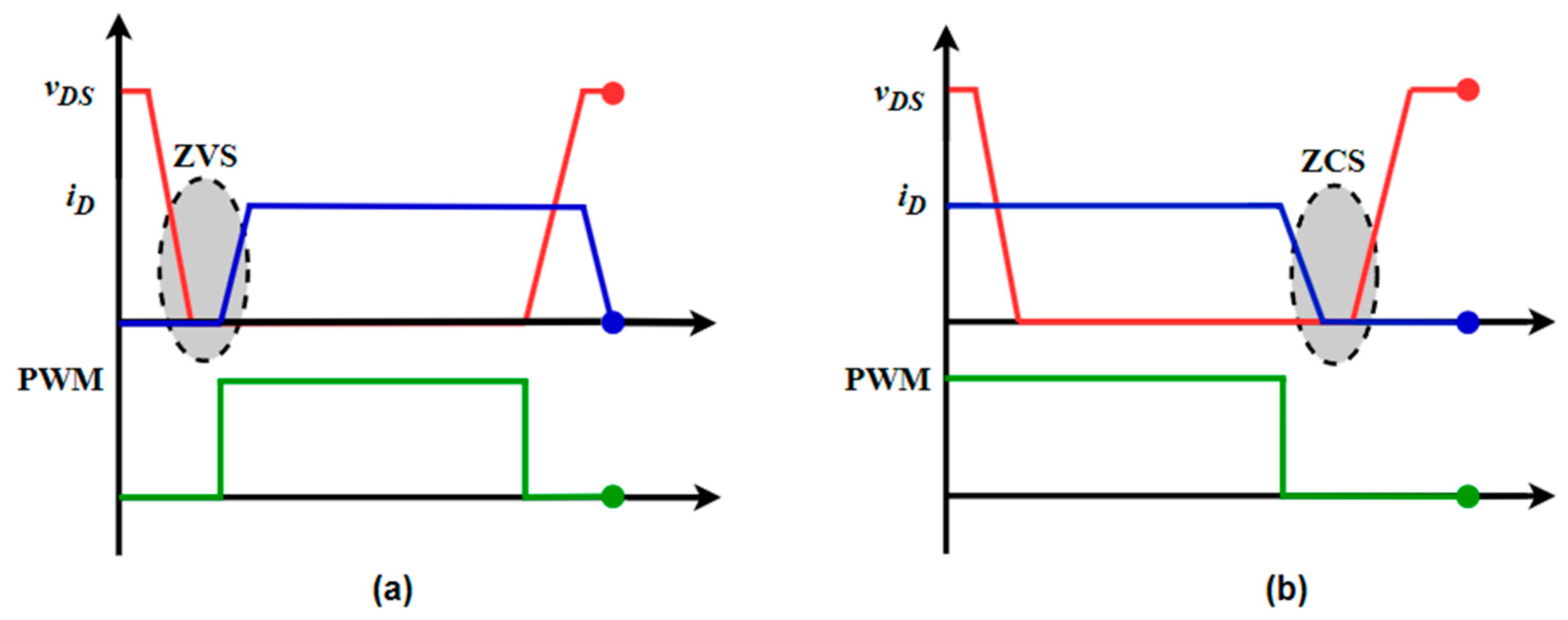
2.3. Soft Switching vs. Hard Switching
2.4. High-Frequency Transformer Design
- Select the core with the “product of area” method using the following equation, where is the input power, is the maximum magnetic flux density, k is the packing factor, and J is the current density:
- 2.
- Determine the number of turns on the primary and secondary sides of the HFT (N1 and N2, respectively) using the following equations, where S represents the cross-sectional area of the magnetic core:
- 3.
- Calculate the cross-sectional area of the wire for and through the following equations, where I1 and I2 represent the current in the primary and secondary windings of the transformer, respectively. ID1 and ID2 represent the current in the diodes, and ILrms represents the rms value of the current in the resonant tank:
- 4.
- Calculate the winding losses (Pp) and the losses in the HFT core (Ps) through several steps to determine the HFT’s global efficiency.
- 4.1.
- Winding losses:
- 4.2.
- Find the HFT core losses using the datasheet for operating conditions.
- 4.3.
- Total sum of losses and calculation of HFT efficiency ():
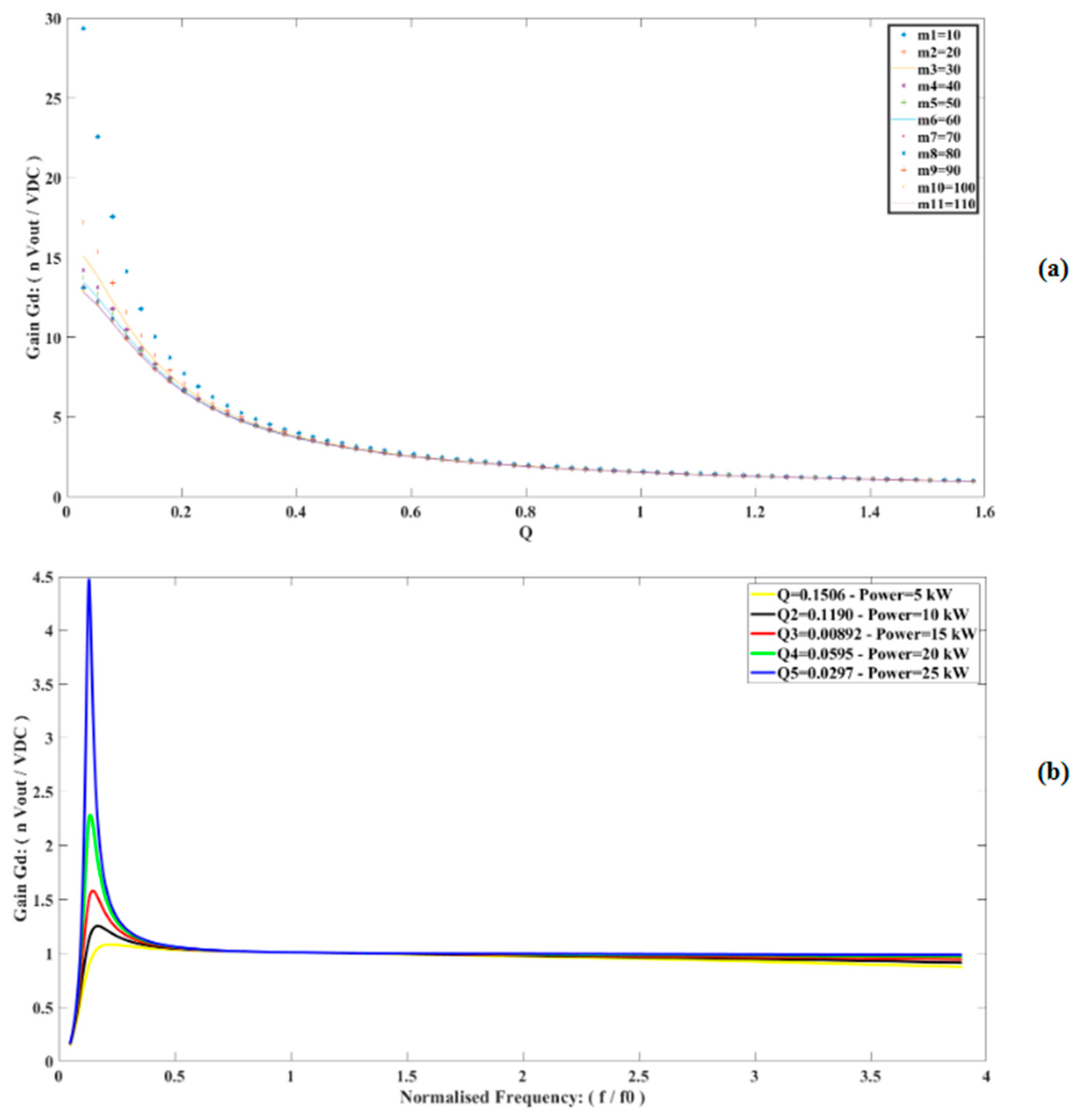
3. Computational Validation
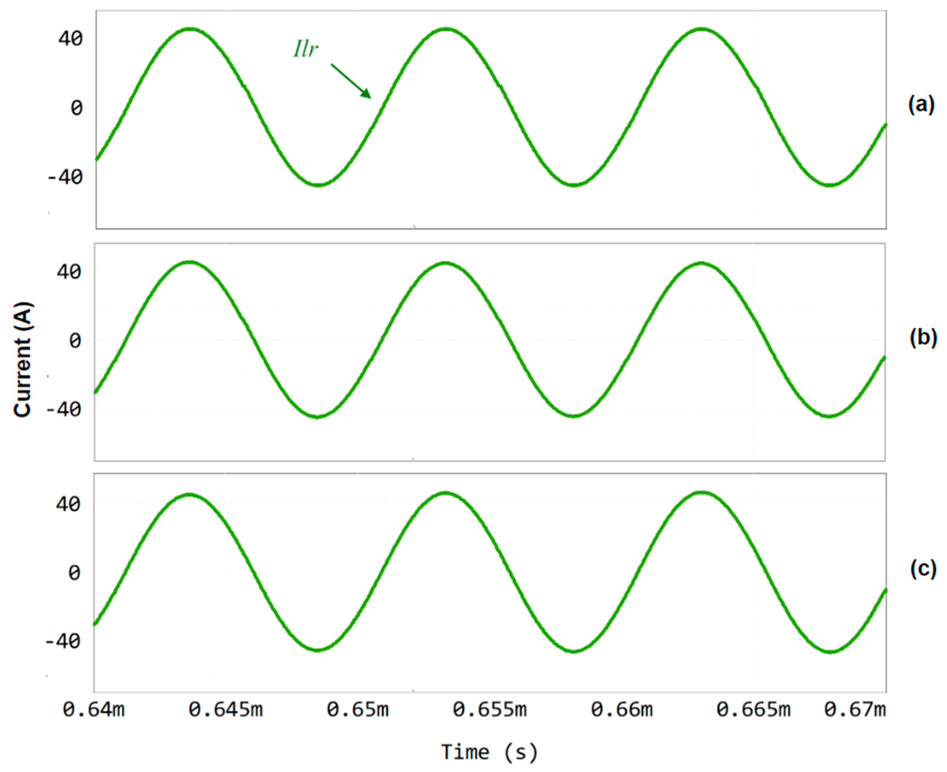
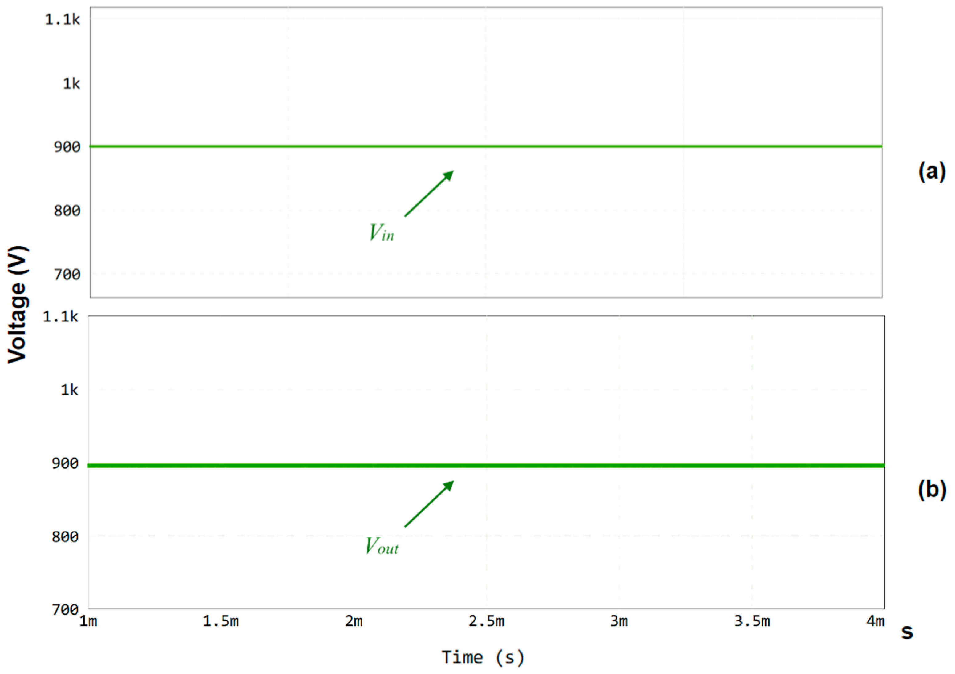
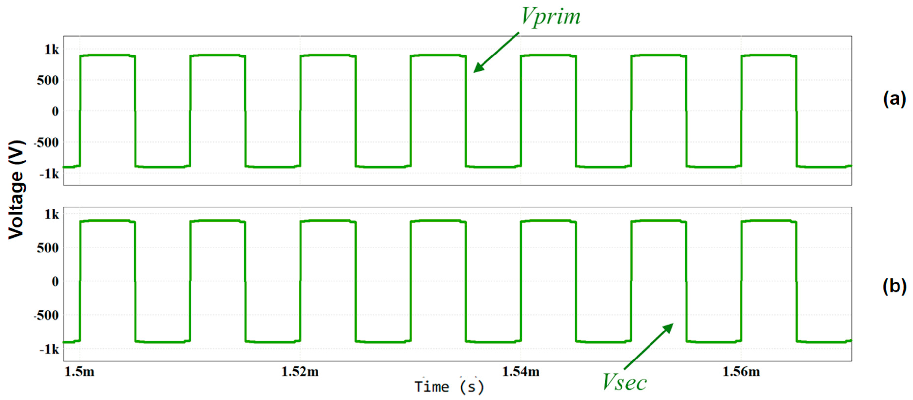
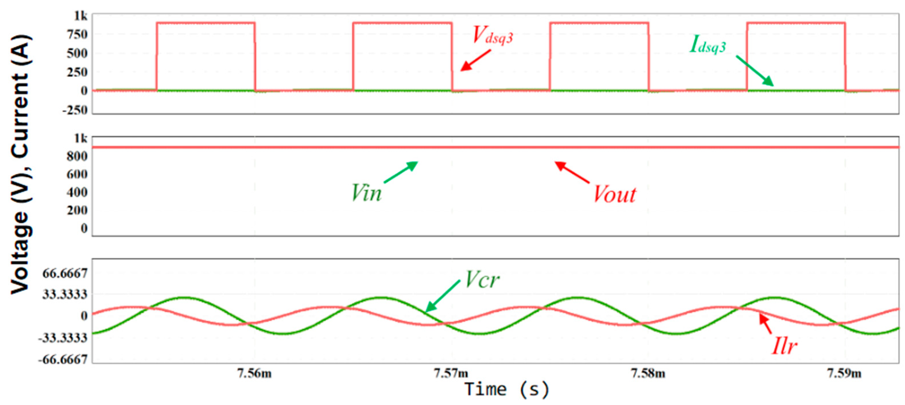
3.1. Operating Principle Validation
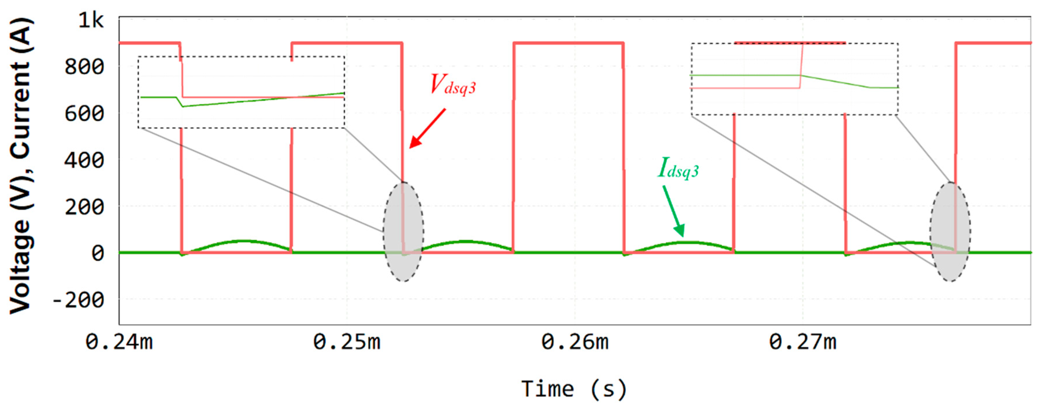
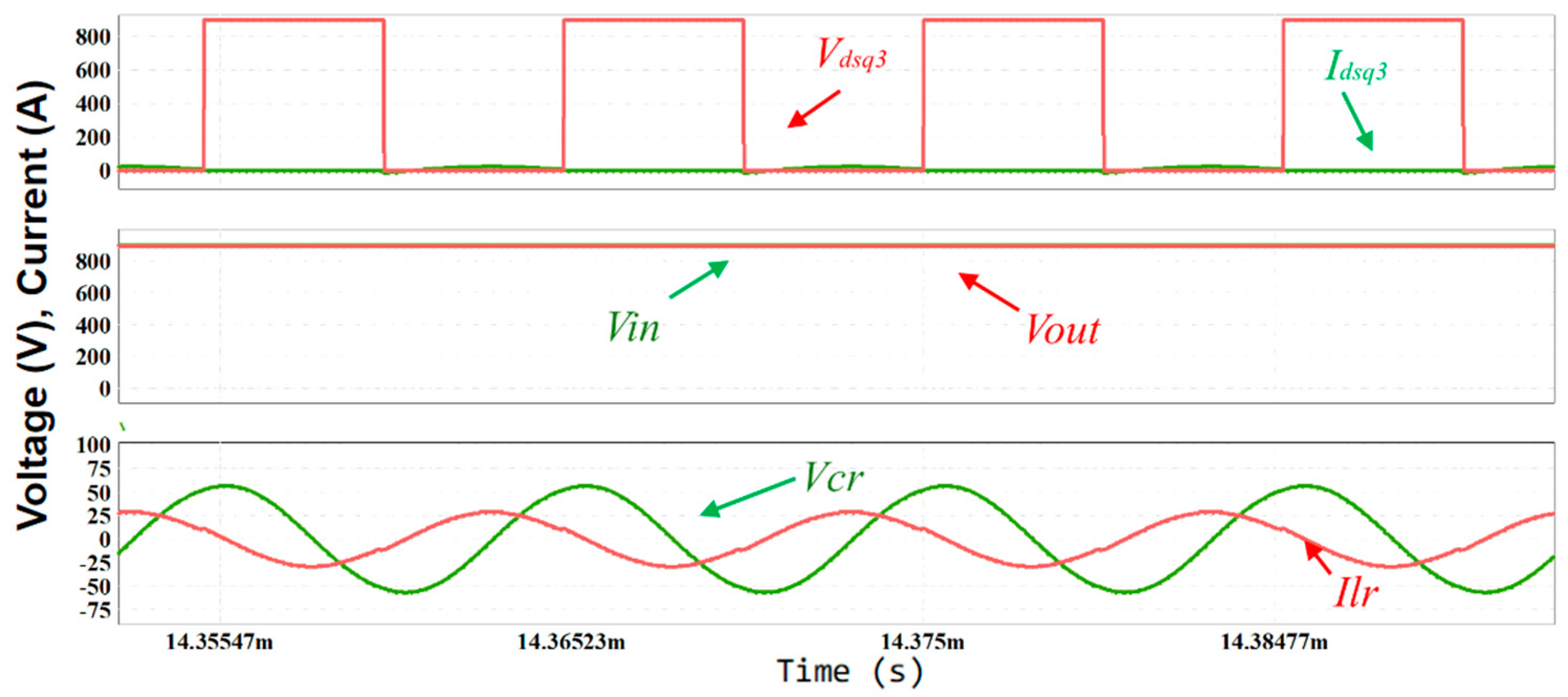
3.2. ZVS and ZCS Control Simulations
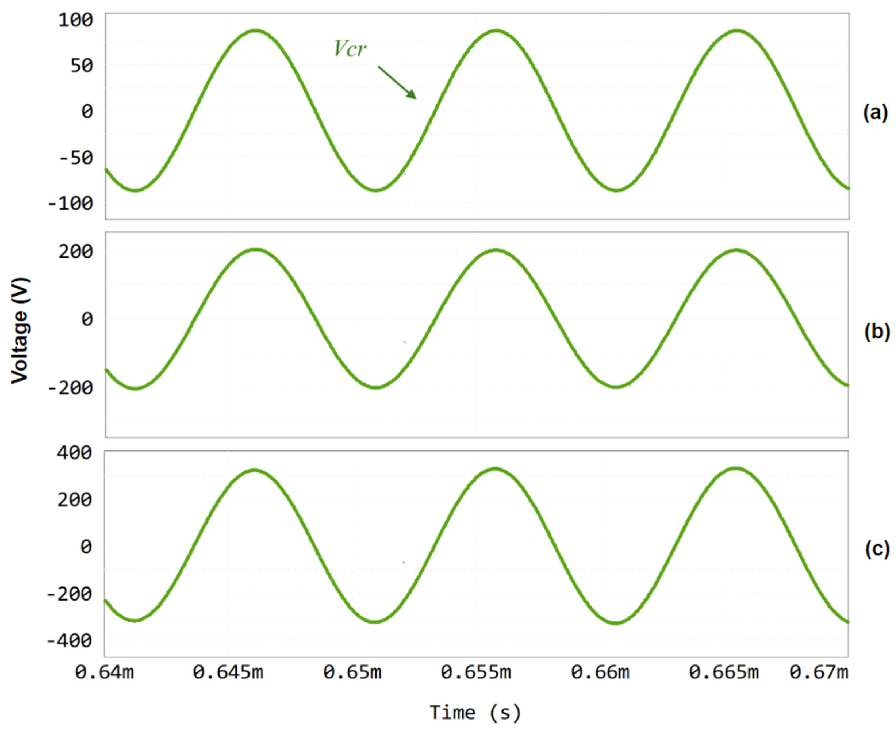
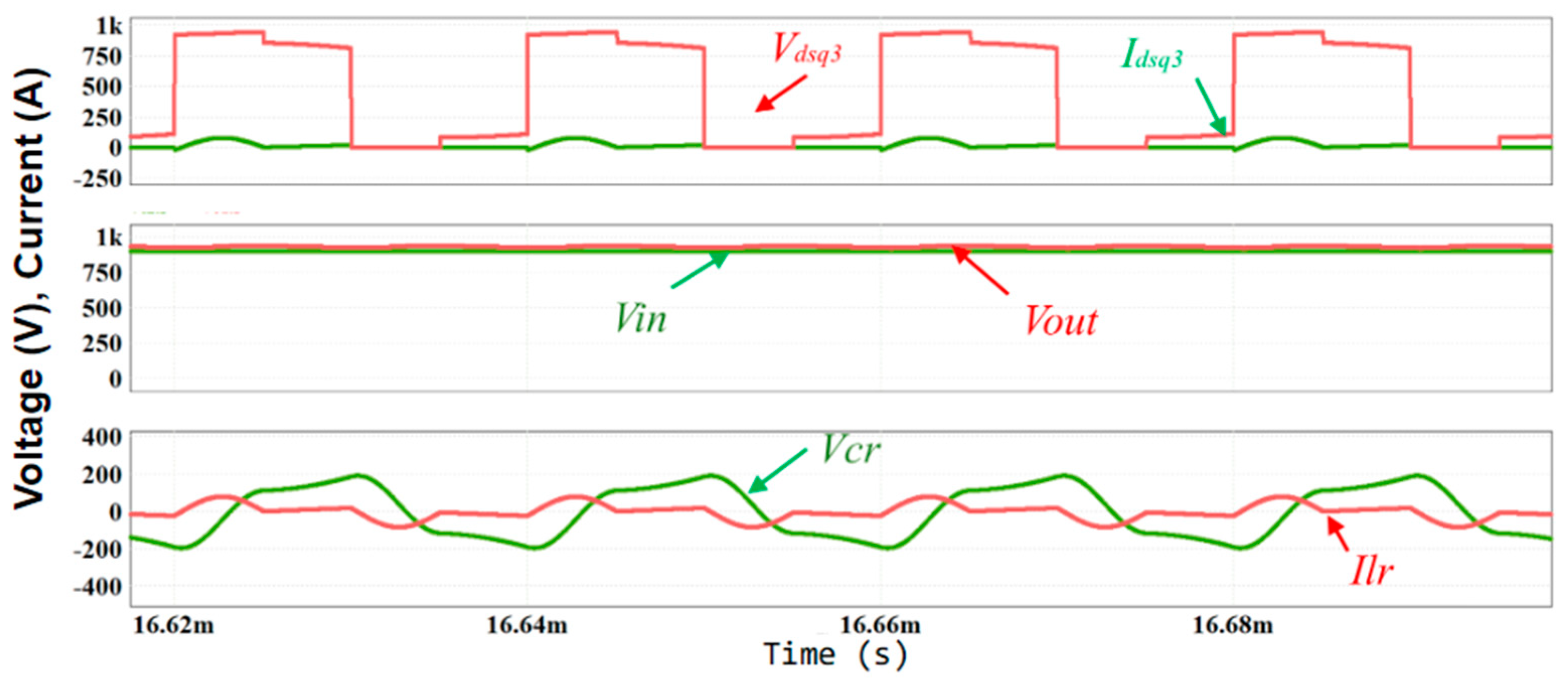
3.3. Influence of Power and Frequency on Converter Operation
4. HFT Development and Prototype Assembly
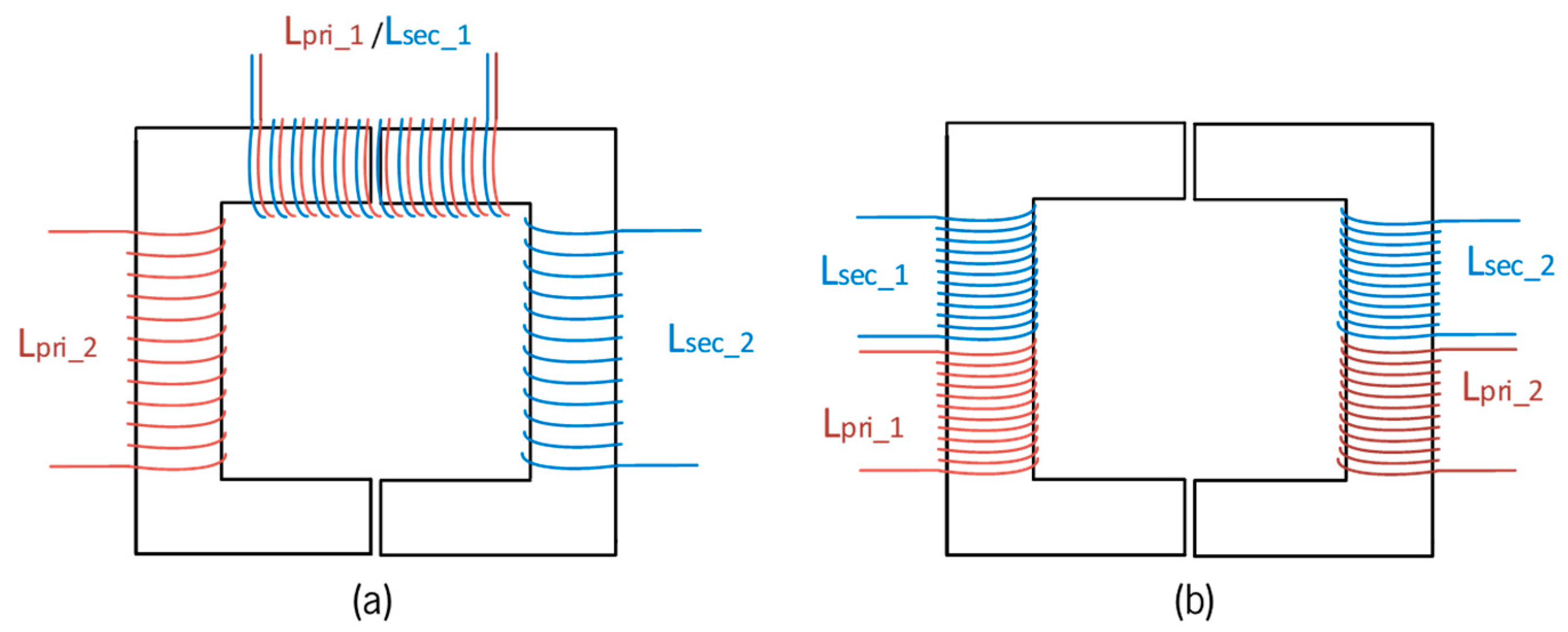
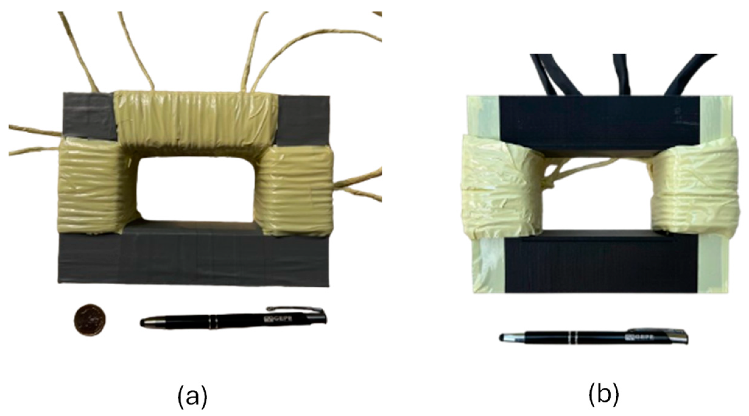
4.1. Implementation of a Real HFT
- Design 1: Wrap 12 turns of the primary and 12 turns of the secondary on top on both sides.
- Design 2: Wrap 6 turns plus 6 primary turns, and then, on top, 6 turns plus 6 secondary turns, repeating on both sides.
- Design 3: Wind 12 primary turns and another 12 secondary turns.
- Design 4: Wind 12 turns plus 12 turns of the primary on one side and 12 turns plus 12 turns on the other side of the secondary.
- Design 5: Wind 12 turns of the primary plus 12 turns of the secondary on each side, using the larger side.
- Design 6: Wind 12 turns plus 12 turns in parallel of the primary plus 12 turns of the secondary on both sides.
- Design 7: Wind 12 turns of the primary on one side plus 12 turns of the secondary on the other side, and then, on the larger side, wind 12 turns of the primary plus 12 turns of the secondary in parallel.
- Design 8: Wind 12 turns of the primary plus 12 turns of the secondary in parallel on one side, and then, 12 turns of the primary plus 12 turns of the secondary on the other.
- Design 9: Wrap 12 turns of the secondary, 12 turns of the primary, 12 turns of the secondary, and 12 turns of the primary divided among the 4 sides.
- Design 10: Wind 12 turns of the primary, 12 turns of the primary, 12 turns of the secondary, and 12 turns of the secondary, changing the order of Design 9.
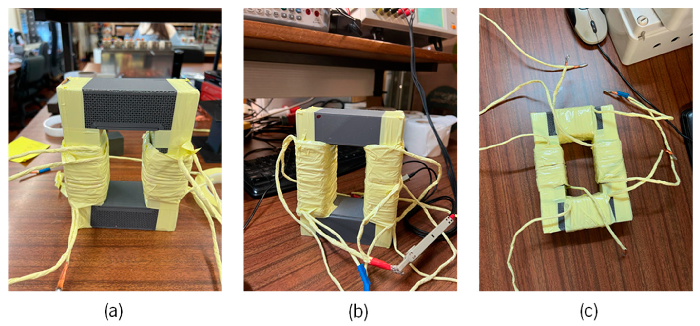
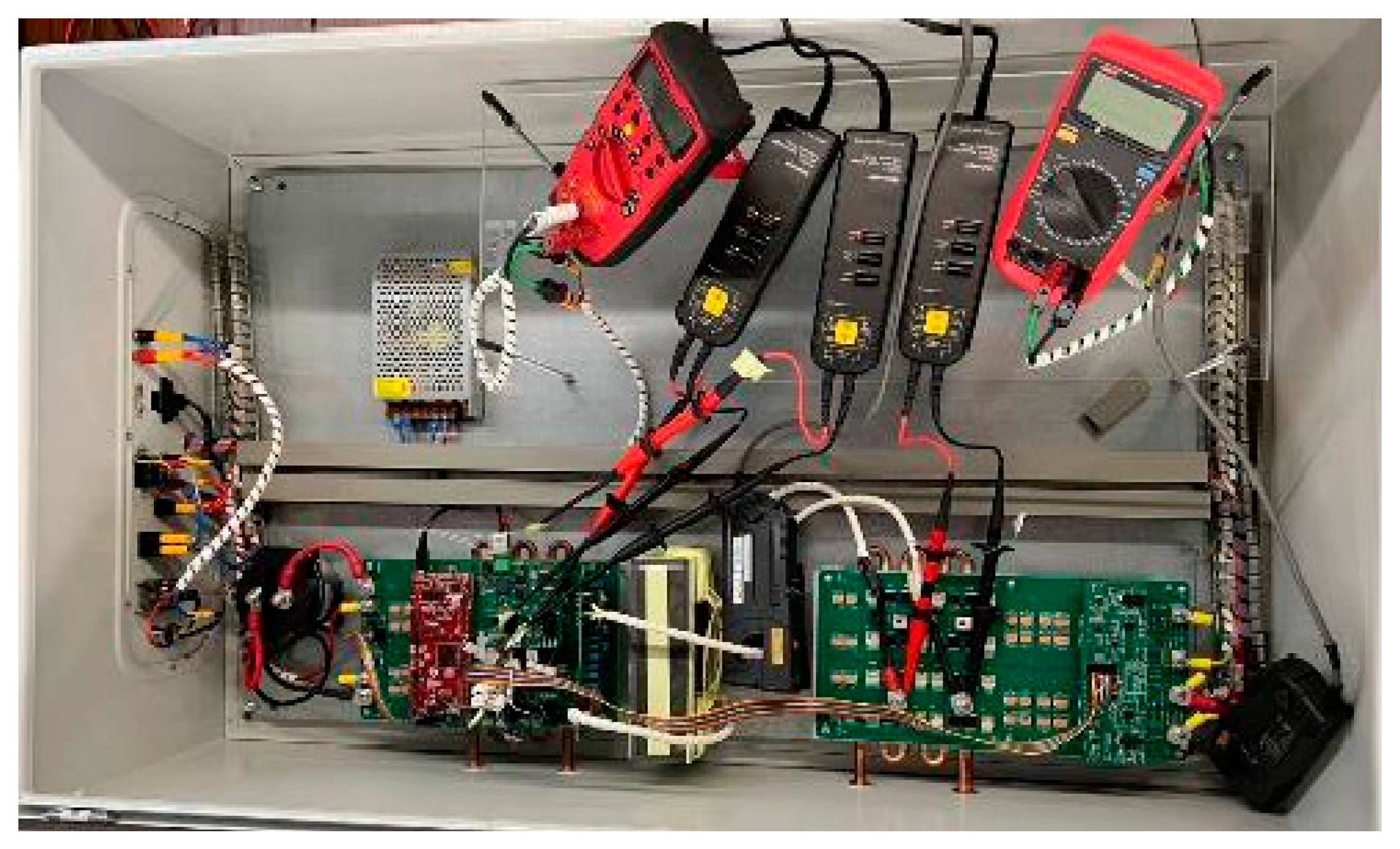
4.2. Prototype Assembly
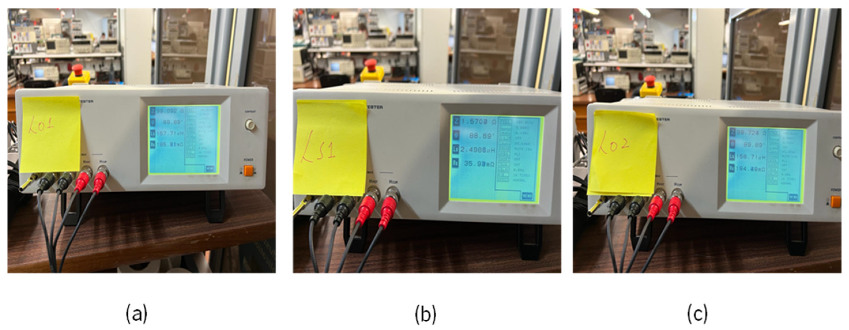
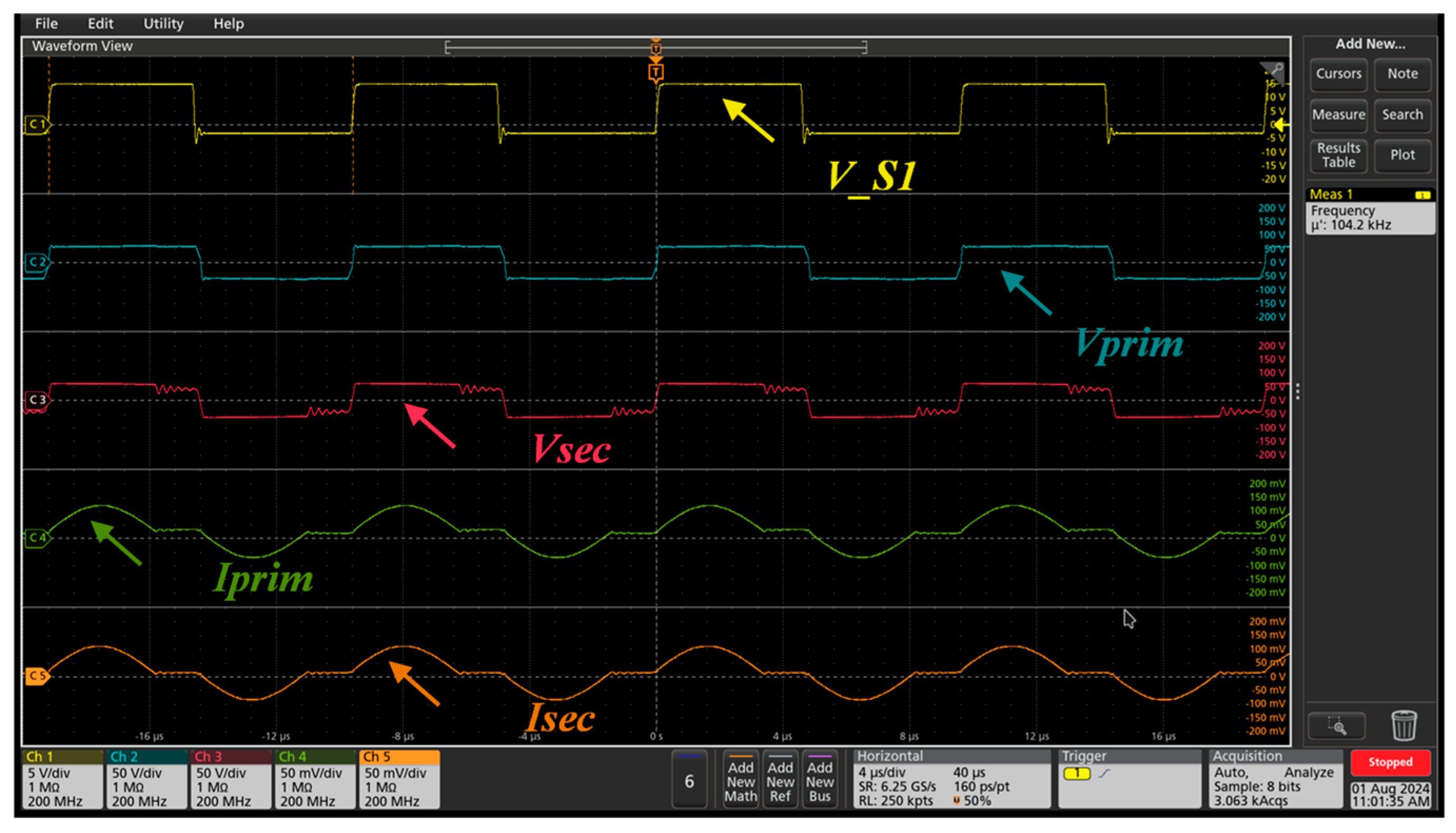
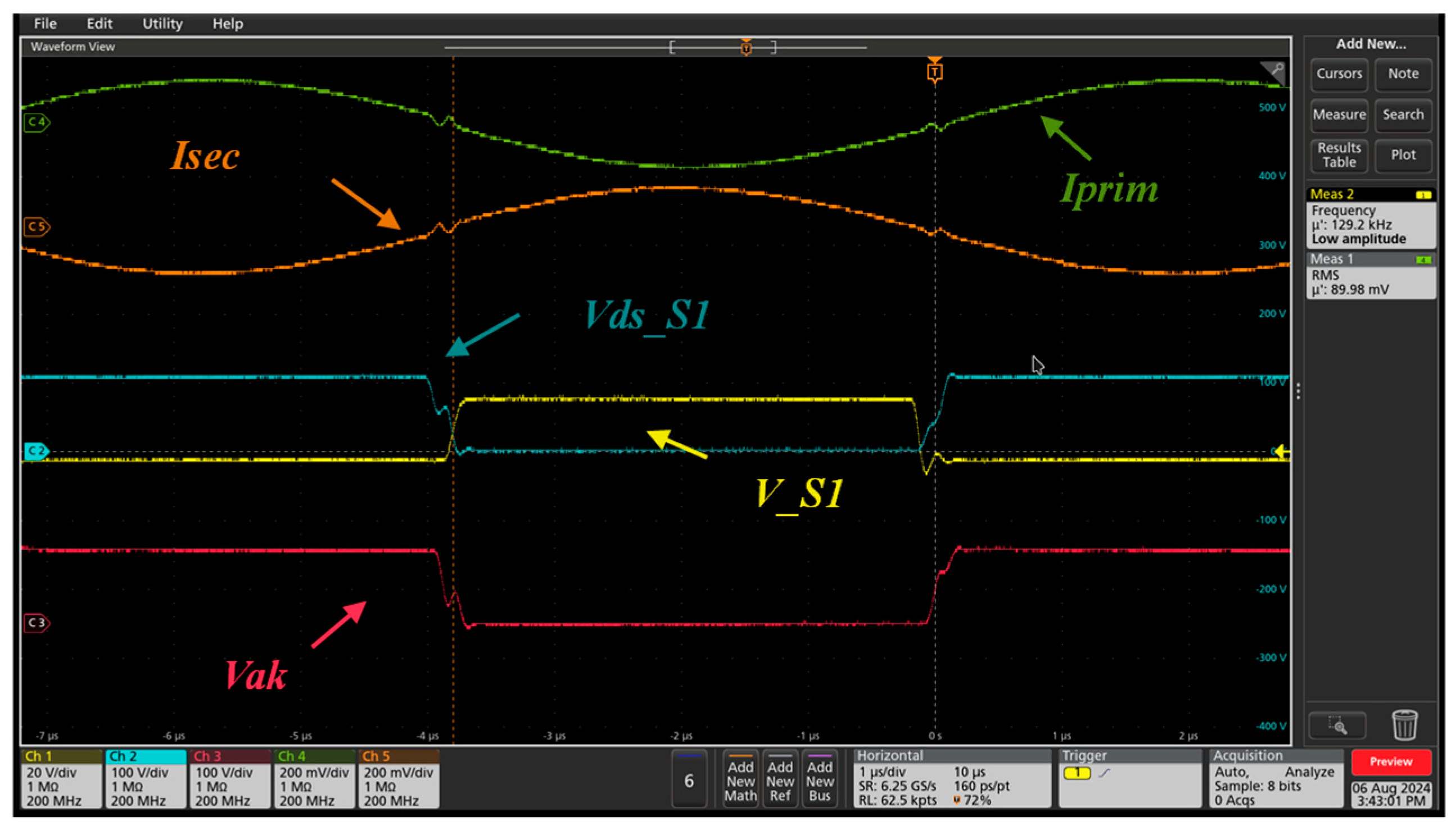
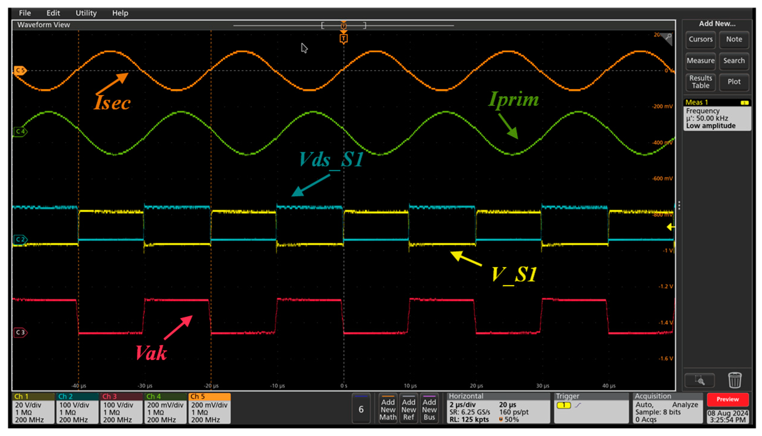
5. Experimental Results
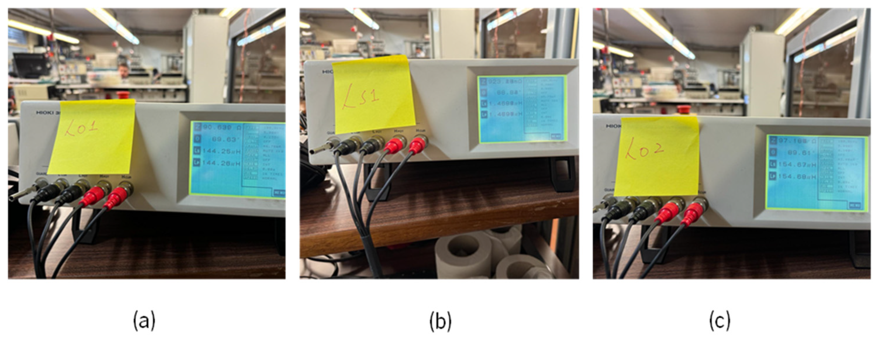
5.1. Test with First HFT Design
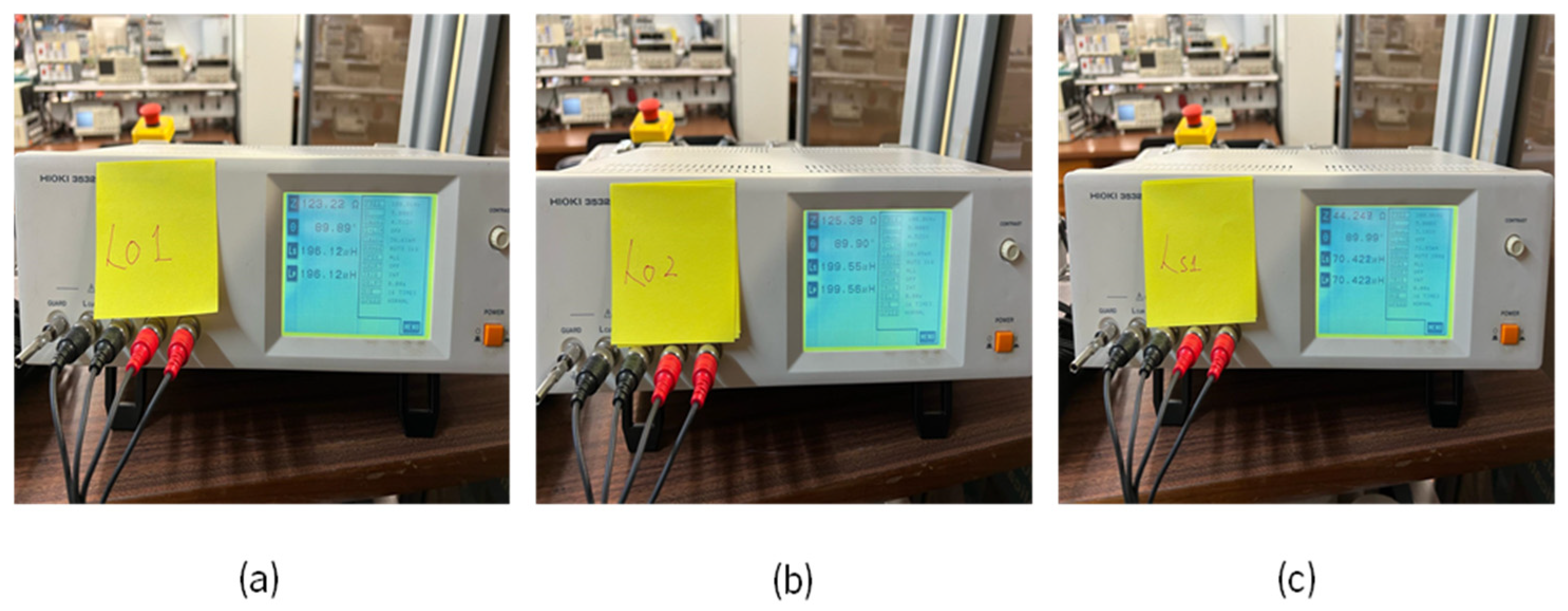
5.2. Test with Second HFT Design
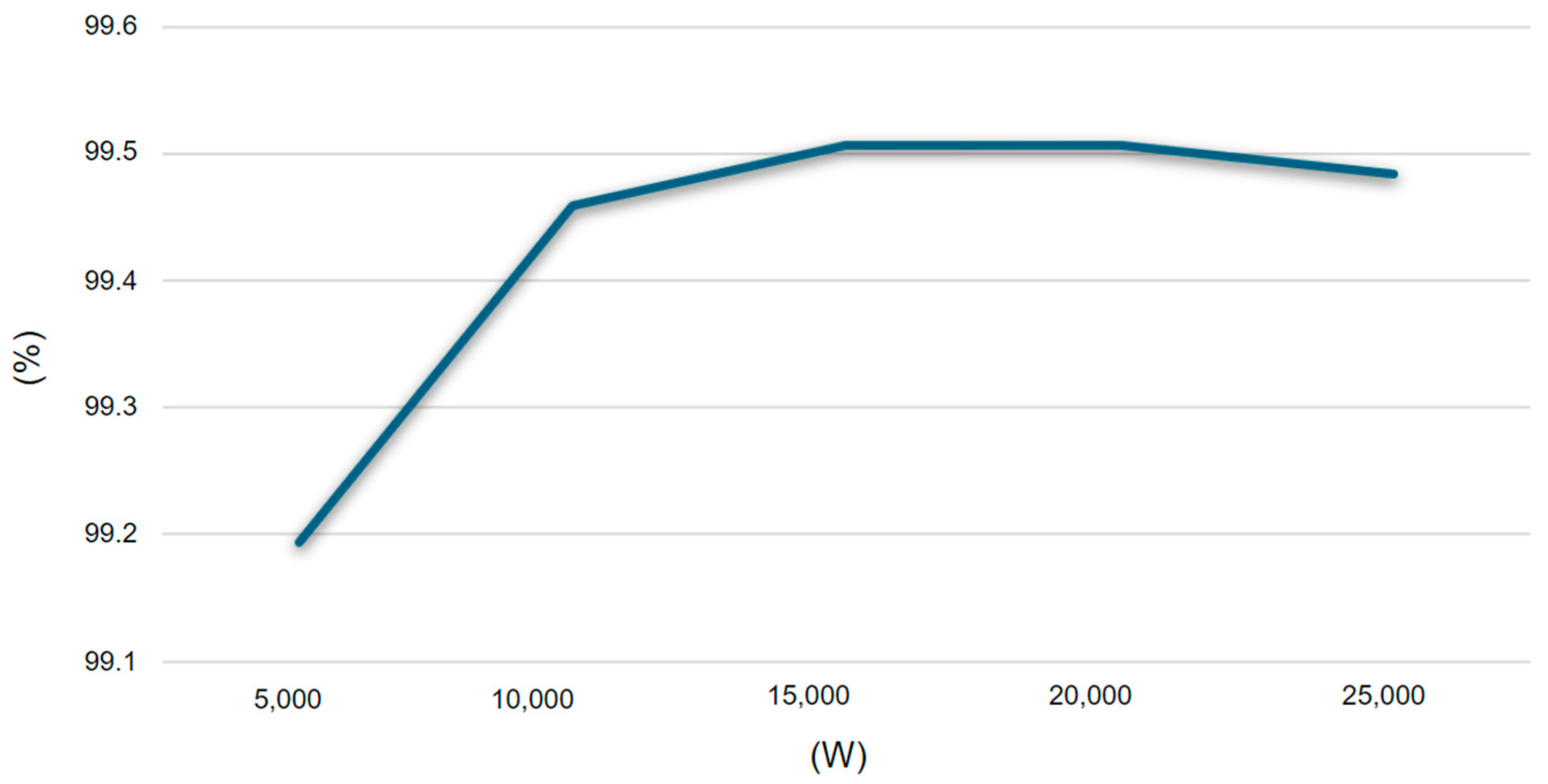
5.3. Efficiency Results
6. Conclusions
Author Contributions
Funding
Data Availability Statement
Conflicts of Interest
References
- Sathiyan, S.P.; Pratap, C.B.; Stonier, A.A.; Peter, G.; Sherine, A.; Praghash, K. Comprehensive Assessment of Electric Vehicle Development, Deployment, and Policy Initiatives to Reduce GHG Emissions: Opportunities and Challenges. IEEE Access 2022, 10, 53614–53639. [Google Scholar] [CrossRef]
- Van der Steen, M.; Van Deventer, P.; De Brujin, H.; van Twist, M.J.W. Governing and Innovation: The Transition to E-Mobility—A Dutch Perspective. World Electr. Veh. J. 2012, 5, 58–71. [Google Scholar] [CrossRef]
- International Energy Agency (IEA). Trends in Electric Cars—Global EV Outlook 2024—Analysis. Available online: https://www.iea.org/reports/global-ev-outlook-2024/trends-in-electric-cars (accessed on 18 November 2024).
- Amin, S.; Rocha, J.; Monteiro, V.; Costa, N. Three-Level Zero-Voltage Transition Interleaved Buck Converter with DC Transformer-based Isolation for EV Fast Charging Stations. In Technological Innovation for Human-Centric Systems, Proceedings of the 15th IFIP WG 5.5/SOCOLNET Advanced Doctoral Conference on Computing, Electrical and Industrial Systems, DoCEIS 2024, Caparica, Portugal, 3–5 July 2024; IFIP Advances in Information and Communication Technology; Camarinha-Matos, L.M., Ferrada, F., Eds.; Springer Nature: Cham, Switzerland, 2024; Volume 716, pp. 244–253. [Google Scholar] [CrossRef]
- Redondo-Iglesias, E.; Vinot, E.; Venet, P.; Pelissier, S. Electric Vehicle Range and Battery Lifetime: A Trade-Off. In Proceedings of the EVS32, Lyon, France, 19–22 May 2019; p. 9. Available online: https://hal.science/hal-02143273 (accessed on 18 November 2024).
- Omahne, V.; Knez, M.; Obrecht, M. Social Aspects of Electric Vehicles Research—Trends and Relations to Sustainable Development Goals. World Electr. Veh. J. 2021, 12, 15. [Google Scholar] [CrossRef]
- Bisoyi, S.; Terang, P.; Pathak, L.; Singh, A.; Singh, S.; Khare, R. Design of an EV Charging System with Improved Performance. In Sustainable Energy and Technological Advancements, Proceedings of the ISSETA Shillong, India, 24–25 September 2021; Springer: Singapore, 2022; pp. 541–558. [Google Scholar] [CrossRef]
- Trivedi, N.; Gujar, N.S.; Sarkar, S.; Pundir, S.P.S. Different fast charging methods and topologies for EV charging. In Proceedings of the 2018 IEEMA Engineer Infinite Conference (eTechNxT), New Delhi, India, 13–14 March 2018; pp. 1–5. [Google Scholar] [CrossRef]
- Saadaoui, A.; Ouassaid, M.; Maaroufi, M. Overview of Integration of Power Electronic Topologies and Advanced Control Techniques of Ultra-Fast EV Charging Stations in Standalone Microgrids. Energies 2023, 16, 1031. [Google Scholar] [CrossRef]
- Safayatullah, M.; Elrais, M.T.; Ghosh, S.; Rezaii, R.; Batarseh, I. A Comprehensive Review of Power Converter Topologies and Control Methods for Electric Vehicle Fast Charging Applications. IEEE Access 2022, 10, 40753–40793. [Google Scholar] [CrossRef]
- Zhou, K.; Wu, Y.; Wu, X.; Sun, Y.; Teng, D.; Liu, Y. Research and Development Review of Power Converter Topologies and Control Technology for Electric Vehicle Fast-Charging Systems. Electronics 2023, 12, 1581. [Google Scholar] [CrossRef]
- Alhurayyis, I.; Elkhateb, A.; Morrow, J. Isolated and Nonisolated DC-to-DC Converters for Medium-Voltage DC Networks: A Review. IEEE J. Emerg. Sel. Top. Power Electron. 2021, 9, 7486–7500. [Google Scholar] [CrossRef]
- Wei, C.; Hu, Z.; Zhang, F.; Shao, J.; Narain, A. A SiC Based 30kW Three-Phase Interleaved LLC Resonant Converter for EV Fast Charger. In Proceedings of the PCIM Europe 2022—International Exhibition and Conference for Power Electronics, Intelligent Motion, Renewable Energy and Energy Management, Nürnberg, Germany, 10–12 May 2022; pp. 1–6. [Google Scholar] [CrossRef]
- Sheng, B.; Zhou, X.; Liu, W.; Chen, Y.; Liu, Y.-F.; Sen, P.C. Analysis and Control of Three-Phase Interleaved SCC-LLC Resonant Converter Load Sharing Considering Component Tolerance. In Proceedings of the 2020 IEEE Energy Conversion Congress and Exposition (ECCE), Detroit, MI, USA, 11–15 October 2020; pp. 385–392. [Google Scholar] [CrossRef]
- Trung, T.H.; Linh, N.H.; Canh, H.V.; Pham, P.V. Unbalanced three-phase interleaved LLC resonant converter: Current phase angle balancing technique. Int. J. Power Electron. Drive Syst. 2022, 13, 1056. [Google Scholar] [CrossRef]
- Hasseni, S. Design and Control of Bidirectional Dual Active Bridge DC-DC Converter for Dynamic Electric Vehicle Charging and Vehicle-to-Grid Operations. Ph.D. Thesis, Glasgow Caledonian Univesiry, Glasgow, UK, 2021. [Google Scholar]
- Eyvazi, H.; Alimohammadi, Z.; Sheikhi, A.; Adelighalehtak, Y.; Poursheykh, T. Analysis of dual active bridge-based on-board battery charger for electric and hybrid vehicles. Int. J. Sci. Res. Arch. 2024, 12, 216–230. [Google Scholar] [CrossRef]
- Mathew, A.; Prasad, U.R.; Madhu, G.M.; Naik, N.; Vyjayanthi, C.; Subudhi, B. Performance Analysis of a Dual Active Bridge Converter in EV Charging Applications. In Proceedings of the 2022 International Conference for Advancement in Technology (ICONAT), Goa, India, 21–22 January 2022; pp. 1–6. [Google Scholar] [CrossRef]
- Coelho, S.; Sousa, T.J.C.; Monteiro, V.D.F.; Machado, L.; Afonso, J.L.; Couto, C. Comparative Analysis and Validation of Different Modulation Strategies for a Dual Active Bridge Converter. Available online: https://repositorium.sdum.uminho.pt/handle/1822/80157 (accessed on 18 November 2024).
- Lim, S.-K.; Lee, H.-S.; Cha, H.-R.; Park, S.-J. Multi-Level DC-DC Converter for E-Mobility Charging Stations. IEEE Access 2020, 8, 48774–48783. [Google Scholar] [CrossRef]
- Kouro, S.; Malinowski, M.; Gopakumar, K.; Pou, J.; Franquelo, L.G.; Wu, B. Recent Advances and Industrial Applications of Multilevel Converters. IEEE Trans. Ind. Electron. 2010, 57, 2533–2580. Available online: https://ieeexplore.ieee.org/document/5482117 (accessed on 18 November 2024). [CrossRef]
- Ngo, T.; Nguyen-Quang, N. Improving Battery Charging Efficiency with Soft Switching Technique. In Proceedings of the 5th World Conference on Applied Sciences, Engineering & Technology, Ho Chi Minh City, Vietnam, 2–4 June 2016. [Google Scholar]
- Kim, D.-H.; Kim, M.-S.; Hussain Nengroo, S.; Kim, C.-H.; Kim, H.-J. LLC Resonant Converter for LEV (Light Electric Vehicle) Fast Chargers. Electronics 2019, 8, 362. [Google Scholar] [CrossRef]
- Elezab, A.; Zaied, O.; Abulnaga, A.; Narimani, M. High-Efficiency LLC Resonant Converter with Wide Output Range of 200–1000 V for DC-Connected EVs Ultra-Fast Charging Stations. IEEE Access 2023, 11, 33037–33048. [Google Scholar] [CrossRef]
- Israr, M.; Samuel, P. Study and Design of DC-DC LLC Full Bridge Converter for Electric Vehicle Charging Application. In Proceedings of the 5th International Conference on Power, Control & Embeded Systems (IPSCES), Allahabad, India, 6–8 January 2023; pp. 1–6. [Google Scholar] [CrossRef]
- Rocha, J.; Amin, S.; Rego, G.; Monteiro, V. Step-by-Step Design of a LLC Resonant Converter for EV Fast Charging Applications. In Proceedings of the 2024 8th International Young Engineers Forum on Electrical and Computer Engineering (YEF-ECE), Caparica/Lisbon, Portugal, 5 July 2024; pp. 45–50. [Google Scholar] [CrossRef]
- Delgado, M.T.; Buja, G.; Czarkowski, D. Resonant Power Converters: An Overview with Multiple Elements in the Resonant Tank Network. IEEE Ind. Electron. Mag. 2016, 10, 21–45. [Google Scholar] [CrossRef]
- Liu, F.; Yan, J.; Ruan, X. Zero-Voltage and Zero-Current-Switching PWM Combined Three-Level DC-DC Converter. IEEE Trans. Ind. Electron. 2010, 57, 1644–1654. [Google Scholar] [CrossRef]
- Lalitha, A.S.; Chakraborty, S.; Kumar, S.S. A Zero Voltage Switching Based Soft Switching Boost DC-DC Converter for Vehicle to Grid Applications with Enhanced Energy Efficiency. In Proceedings of the 2022 3rd International Conference for Emerging Technology (INCET), Belgaum, India, 27–29 May 2022; pp. 1–6. [Google Scholar] [CrossRef]
- Cittanti, D.; Gammeter, C.; Huber, J.; Bojoi, R. A Simplified Hard-Switching Loss Model for Fast-Switching Three-Level T-Type SiC Bridge-Legs. Electronics 2022, 11, 1686. [Google Scholar] [CrossRef]
- Abdulhakeem, M.; Sahid, M.R.; Sutikno, T. Overview of Soft-Switching DC-DC Converters. Int. J. Power Electron. Drive Syst. IJPEDS 2006, 9, 2006. [Google Scholar] [CrossRef]
- Riegler, B.; Mütze, A. Volume Comparison of Passive Components for Hard-Switching Current- and Voltage-Source-Inverters. In Proceedings of the 2021 IEEE Energy Conversion Congress and Exposition (ECCE), Vancouver, BC, Canada, 10–14 October 2021; pp. 1902–1909. [Google Scholar] [CrossRef]
- Ebli, M.; Pfost, M. An analysis of the switching behavior of GaN-HEMTs. In Proceedings of the 2017 International Symposium on Signals, Circuits, and Systems (ISSCS), Iasi, Romania, 13–14 July 2017; pp. 1–4. [Google Scholar] [CrossRef]
- Lee, I.-O.; Moon, G.-W. Soft-Switching DC-DC Converter With a Full ZVS Range and Reduced Output Filter for High-Voltage Applications. IEEE Trans. Power Electron. 2023, 28, 112–122. [Google Scholar] [CrossRef]
- Nadolny, Z. Design and Optimization of Power Transformer Diagnostics. Energies 2023, 16, 6466. [Google Scholar] [CrossRef]
- Khosrogorji, S.; Soori, S.; Torkaman, H. A new design strategy for DC-DC LLC resonant converter: Concept, modeling, and fabrication. Int. J. Circuit Theory Appl. 2019, 47, 1645–1663. [Google Scholar] [CrossRef]
- Sucameli, M.; Adragna, C. LLC Resonant Converters as Isolated Power Factor Corrector Pre-Regulators—Analysis and Performance Evaluation. Energies 2023, 16, 7114. [Google Scholar] [CrossRef]
- Liu, Y.-C.; Chen, C.; Chen, K.-D.; Syu, Y.-L.; Tsai, M.-C. High-Frequency LLC Resonant Converter with GaN Devices and Integrated Magnetics. Energies 2019, 12, 1781. [Google Scholar] [CrossRef]


| Advantages | Disadvantages | |
|---|---|---|
| Interleaved Three-Phase LLC Resonant |
|
|
| DAB |
|
|
| Multilevel |
|
|
| LLC Resonant |
|
|
| Parameters | Value |
|---|---|
| Input voltage | 900 V |
| Output voltage | 900 V |
| Operating power | 5 kW to 25 kW |
| Switching frequency, fsw | 100 kHz |
| HFT transformation ratio | 1:1 |
| MOSFET model | G3R30MT12J |
| Diode model | GD30NPS12J |
| Output capacitor | 10 µF |
| Design 1 | 144 µH | 154 µH | 1.47 µH |
| Design 2 | 179 µH | 180 µH | 12.86 µH |
| Design 3 | 176 µH | 177 µH | 19.2 µH |
| Design 4 | 196 µH | 199 µH | 70 µH |
| Design 5 | 163 µH | 175 µH | 1.7 µH |
| Design 6 | 156 µH | 157 µH | 1.32 µH |
| Design 7 | 163 µH | 163 µH | 3 µH |
| Design 8 | 157 µH | 158 µH | 2.5 µH |
| Design 9 | 158 µH | 196 µH | 18 µH |
| Design 10 | 168 µH | 170 µH | 32 µH |
Disclaimer/Publisher’s Note: The statements, opinions and data contained in all publications are solely those of the individual author(s) and contributor(s) and not of MDPI and/or the editor(s). MDPI and/or the editor(s) disclaim responsibility for any injury to people or property resulting from any ideas, methods, instructions or products referred to in the content. |
© 2025 by the authors. Licensee MDPI, Basel, Switzerland. This article is an open access article distributed under the terms and conditions of the Creative Commons Attribution (CC BY) license (https://creativecommons.org/licenses/by/4.0/).
Share and Cite
Rocha, J.; Amin, S.; Coelho, S.; Rego, G.; Afonso, J.L.; Monteiro, V. Design and Implementation of a DC–DC Resonant LLC Converter for Electric Vehicle Fast Chargers. Energies 2025, 18, 1099. https://doi.org/10.3390/en18051099
Rocha J, Amin S, Coelho S, Rego G, Afonso JL, Monteiro V. Design and Implementation of a DC–DC Resonant LLC Converter for Electric Vehicle Fast Chargers. Energies. 2025; 18(5):1099. https://doi.org/10.3390/en18051099
Chicago/Turabian StyleRocha, Joao, Saghir Amin, Sergio Coelho, Gonçalo Rego, Joao L. Afonso, and Vitor Monteiro. 2025. "Design and Implementation of a DC–DC Resonant LLC Converter for Electric Vehicle Fast Chargers" Energies 18, no. 5: 1099. https://doi.org/10.3390/en18051099
APA StyleRocha, J., Amin, S., Coelho, S., Rego, G., Afonso, J. L., & Monteiro, V. (2025). Design and Implementation of a DC–DC Resonant LLC Converter for Electric Vehicle Fast Chargers. Energies, 18(5), 1099. https://doi.org/10.3390/en18051099