Article

Innovative Capacitive Wireless Power System for Machines and Devices

by
Marcin Skóra
1,*,
Joanna Rogala-Rojek
1,
Sebastian Jendrysik
1,
Krzysztof Stankiewicz
1,
Bartosz Polnik
1,
Zbigniew Kaczmarczyk
2,
Marcin Kasprzak
2,
Paweł Lasek
2 and
Krzysztof Przybyła
2
1
KOMAG Institute of Mining Technology, Pszczyńska 37, 44-100 Gliwice, Poland
2
Power Electronics Electrical Drives and Robotics Department (KENER), Silesian University of Technology, Krzywoustego Str. No. 2, 44-100 Gliwice, Poland
*
Author to whom correspondence should be addressed.
Energies 2025, 18(3), 521; https://doi.org/10.3390/en18030521
Submission received: 28 October 2024 / Revised: 13 January 2025 / Accepted: 15 January 2025 / Published: 23 January 2025
(This article belongs to the Special Issue Energy Security and Just Transition)

Abstract

:
This article deals with the design, development, and analysis of a wireless power transfer system prototype based on capacitive coupling. The system is intended for the continuous charging of a suspended mine drivetrain. It consists of a resonant inverter, primary and secondary matching circuits, a suitable capacitive coupler, and a rectifier with a load, ultimately serving as a battery charger for a mobile energy storage device. The system successfully achieved the target output voltage of 320 V and a charger output power of 2 kW at an operating frequency of 300 kHz. Additionally, the total system efficiency was at the level of 60%, ensuring that the RMS voltages on passive components remained below 3 kV.

1. Introduction

The research presented in this article was carried out within the project of the “Innovative high efficiency power system for machines and devices, increasing the level of work safety in underground mining excavations” (HEET II) project co-financed by the European Commission Research Fund for Coal and Steel (RFCS).
Wireless powering of Wireless Energy Transfer (WET) devices is a very attractive and accessible application. It is typically achieved via a magnetic field and, increasingly, using an electric field, resulting in Inductive Wireless Energy Transfer (IWET) [1,2,3] or Capacitive Wireless Energy Transfer (CWET) [1,3,4], or employing both methods simultaneously [5,6]. The distinguishing features of CWET systems include the following: the elimination of eddy currents and the ability to work with metal devices, the use of short and simple metal plates, and the minimization of EMI disturbances during transmission over limited distances. These systems also facilitate the easy powering of multiple receivers. However, they often exhibit low capacitive coupling, which requires an increase in operating frequency to manage voltage levels effectively. CWET systems are used in various fields, including biomedical devices [7], consumer electronics [8], electric drives [9], mobile robots [10], and battery-powered electric vehicles [11,12,13,14,15,16].
This article focuses on the CWET system, with the solution shown in Figure 1. Additionally, it includes a diagram of the simplified power supply path, as provided by the First Harmonic Approximation (FHA) method. The system consists of a supply source, a resonant inverter, matching primary and secondary circuits with a capacitive coupler between them, an output rectifier with a capacitive filter, and a load. This solution represents a further step in the development of a proposal aimed at developing a method for powering electrical machines and equipment, including those in motion, and for use in underground mines. The motivation includes preparing a power supply system capable of recharging machine batteries to extend the operating time of machines on a single charge (beyond the length of the working shift) or, optionally, to reduce the battery. Example calculations related to this are presented in [17]. To the authors’ knowledge, such an application of the CWET system has not been presented to date.
The solution is based on phenomena known from the literature and employs a capacitive coupling structure described as a horizontal four plate [18]. A key consideration during the design was to ensure that the prototype CWET system could be mechanically integrated with the existing mine infrastructure. This would allow it to be used with an example machine, such as a battery-powered suspended drivetrain, moving along a suspended route in a mine roadway.
Another constraint was that the target system would be subjected to a certification and approval testing process before regular operation. Due to the planned use in underground mines, important considerations included the selection of materials, appropriate housing of equipment, and the control of the insulation resistance of cables, as required by mining regulations and the ATEX directive. However, these issues are beyond the scope of this article.
The operation of a CWET system involves a relatively high voltage (a few kilovolts) at a high frequency (300 kHz). Therefore, safety considerations, such as high electrical strength of insulation and maintaining low levels of electric field strength that could affect the operator, are crucial. However, the CWET system relies on resonance during its operation. Therefore, any disturbances, such as wire damage, can disrupt resonance and lead to voltage decay. Additionally, as the voltage frequency increases, the shock current values, which cause the same pathological effects in the case of human contact as the 50 Hz current, also increase [19].
The discussed CWET system is powered from the master energy transmission system via one cable (SWET—Single Wire Energy Transfer), as illustrated in Figure 2. The SWET system includes a rectifier (REC1) enabling active Power Factor Correction (PFC), a resonant inverter (INV1), step-up (TR1), and step-down (TR2) transformers, connected by a high-voltage coaxial cable, and an output rectifier (REC2). The increased operating frequency and increased voltage of the energy transmission path ensure its compactness. The output inverter (INV2) supplies local three-phase receivers in a 3 × 500 V 50 Hz network, while the CWET system is directly powered by an intermediate 800 V DC circuit. The CWET system is designed for static and dynamic charging of batteries integrated with a suspended mine monorail, thereby extending its effective operating time. It can also be used to continuously power low-power receivers (30–50 W), such as those used for communication and measurements. These optional modules, marked as Access Point in Figure 2, are constructed similarly to the main part of the CWET system but they are adapted for an output voltage of 24 V DC. The assumed input power of the SWET system is 8 kW, while the CWET system should deliver sufficient power to charge the batteries at a level of 2 kW.
Many solutions of primary and secondary matching circuits and various capacitive coupler configurations are known in the literature. Resonant matching circuits simultaneously filter and adjust voltage and current levels. Topologies with various cascade connections of passive components are used [11,12,15,18,20], for example, marked as LC, LCL, LCLC, and CLLC. The primary and secondary circuits may be the same or may form combinations. In this way, the properties of the CWET system are shaped in ratio of the output and input voltages, the required output voltage or current character, and the behaviour with changes in capacitive coupling. The capacitive coupler confutations differ in the number and relative (horizontal or vertical) position of their plates [11,12,13,18].
The primary novelties of this article, in contrast to prior studies, involve the use of a more advanced LCLC-CL topology for the CWET system, along with its construction, implementation, and testing under target operating conditions. This concept modifies the solution proposed in [15] and extends the CWET system previously developed by the authors in [17,21]. The new LCLC-CL topology is an adaptation of the LCL-L topology introduced in [15]. The parameters of the matching circuits were selected differently compared to the method proposed in [15]. This topology enables easy tuning to meet the required operating conditions by adjusting the capacitances of the variable capacitors connected at the input and output of the capacitive coupler. The primary plates are appropriately integrated with the support rail of the suspended mine monorail, while the secondary plates move with the railway. The results of laboratory tests of the CWET system and the results of tests carried out in mine conditions (in situ) are included in the article. The process of starting (tuning) the CWET system and its cooperation with other systems developed as part of the HEET II project are presented.

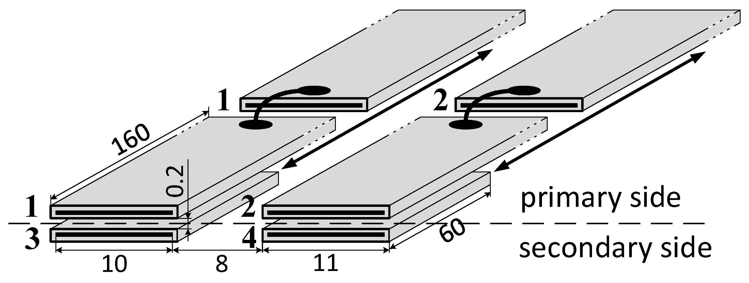
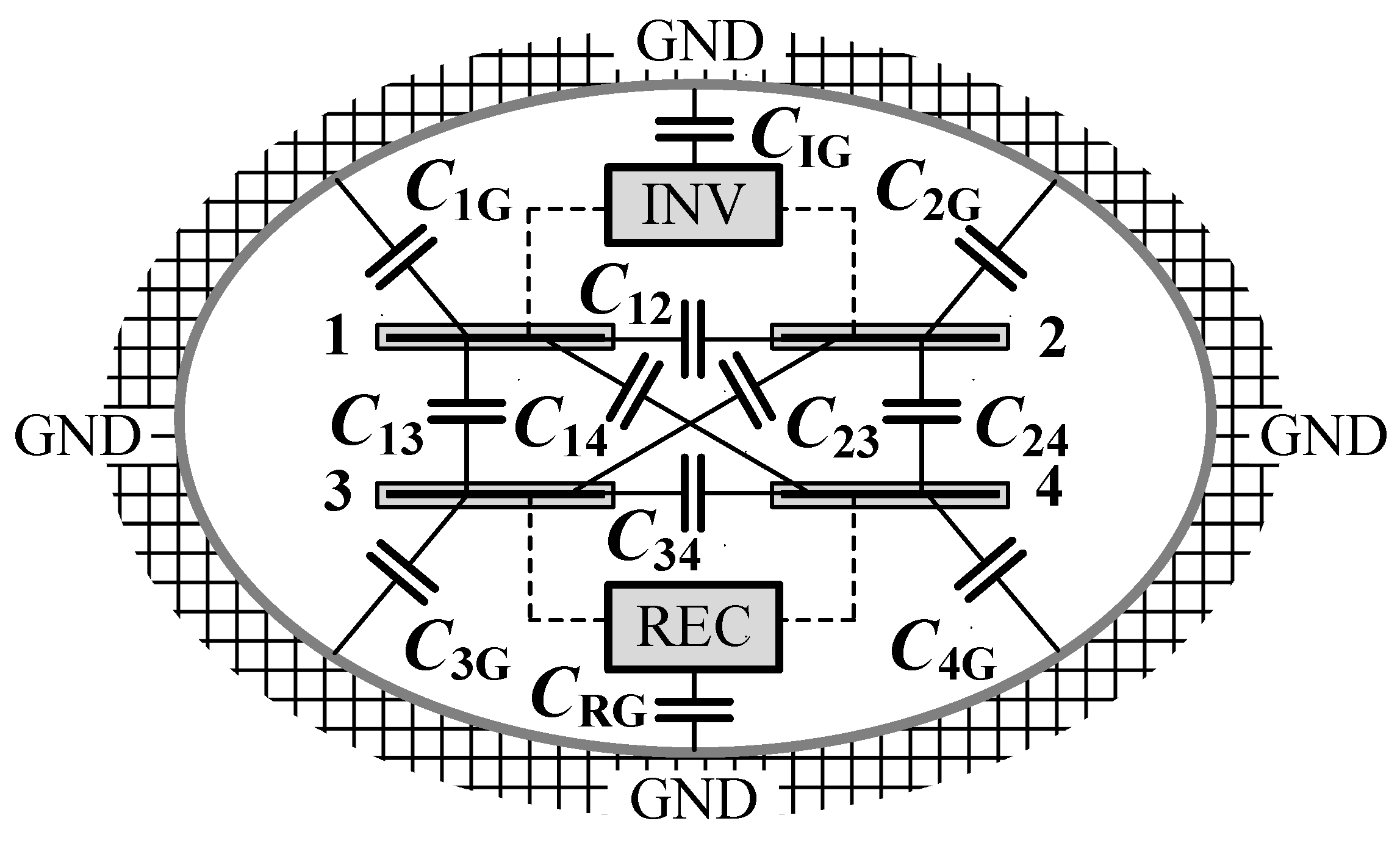
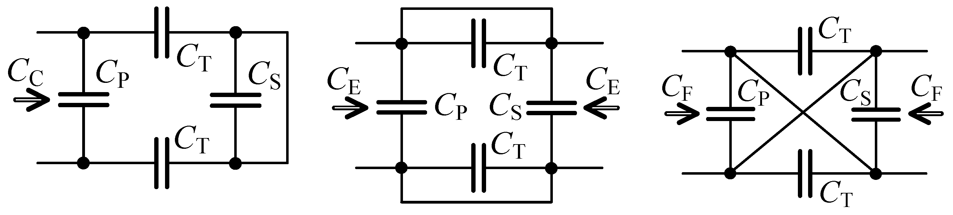
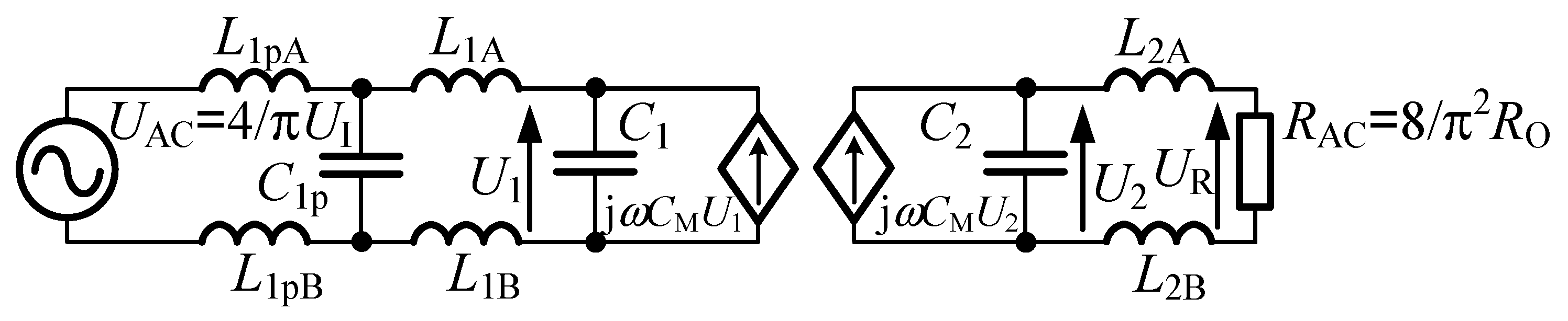
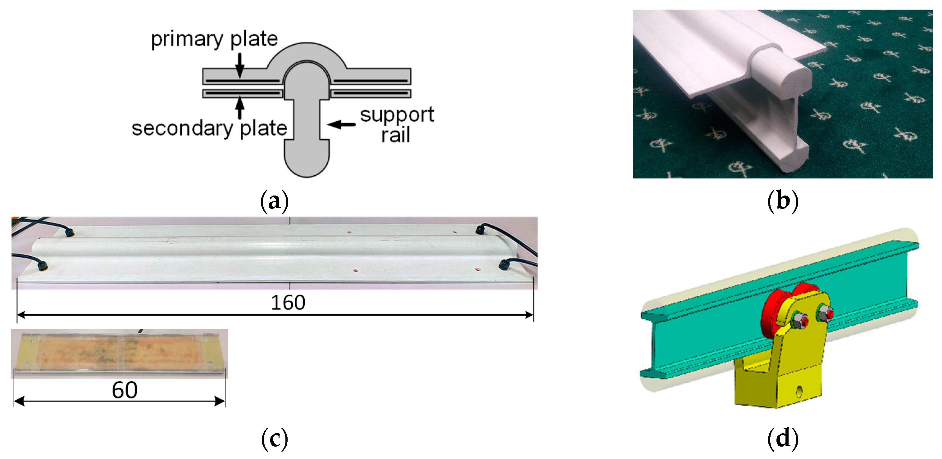
2. Capacitive Coupler

The description of the CWET system starts by detailing the configuration and method for identifying the electrical parameters of the capacitive coupler, as simplified in Figure 3. It consists of two long, stationary, powered primary plates (1 and 2) and two short, movable, receiving secondary plates (3 and 4). These plates are constructed from copper tape, surrounded by load-bearing epoxy insulation. The air gap between the plates is approximately 2 mm. The primary plates are extended by adding subsequent sections.
Determining the electrical parameters of the capacitive coupler is crucial for designing the CWET system. For this purpose, the experimental method proposed in [14] was used. Figure 4 illustrates the set of plates, an inverter, and a rectifier, along with their interaction with the surrounding conductive ground (GND). As any two conductors separated by a dielectric form a capacitor, multiple capacitive components can be identified. These include inter-plate capacitances (C12, C13, C14, C23, C24, C34), the ground capacitances of the plates (C1G, C2G, C3G, C4G), and the ground capacitances associated with the inverter (CIG) and rectifier (CRG). The capacitances C13 and C24 are the main capacitances between the primary and secondary plates. The remaining capacitances can be described as parasitic, making energy transmission difficult. These unavoidable capacitances create unwanted current flow paths, reducing the capacitive coupling. According to the detailed analysis in [14], if a symmetrical matching circuit design and a symmetrical capacitive coupler configuration are adopted, the analysis is simplified to equivalent schemes shown in Figure 5 [12,14]. The first diagram (Figure 5a) is used to identify the parameters of the capacitive coupler, while the second one (Figure 5b) corresponds to the FHA method.
The method for identifying the capacitive coupler parameters has several variations [14], requiring at least three independent capacitance measurements. The selected three capacitance measurements are shown in Figure 6. The capacitance CC, CE, CF (Table 1) were taken for the constructed capacitive coupler discussed in the part of the laboratory tests (Section 5). Based on these measurements and using the Equations (1)–(3) [14], parameters of the capacitive coupler were calculated.
C P = 4 C C + C E C F 4 = 1554   p F
C S = 4 C C + 3 C E + C F 4 = 102   p F
C T = C E + C F 2 = 402   p F

3. Method for Selecting the Matching Circuits Parameters

The matching circuits of the CWET system were selected to create the LCL-L topology shown in Figure 7 and proposed in [15]. As previously explained, a symmetrical circuit configuration was used (L1pA = L1pB = L1p/2, L1A = L1B = L1/2, L2A = L2B = L2/2). This simplifies the analysis and, if the parameters are properly selected, provides approximately constant voltage gain, making the CWET system a voltage source. This will provide the desired output voltage stiffness without the need for feedback. However, note that degrading the capacitive coupling (reducing CT or CM in Figure 5) causes this voltage to decrease proportionally. The method for selecting the parameters of the LCL-L matching circuits is carried out using the FHA method, based on the adapted relationships (4)–(9) from [15]. The analysis assumes linearity and no losses in components for both the inverter and rectifier. Additionally, the same coils L1 and L2 are used (XL1 = XL2). Relationship (9) is obtained by transforming the expressions (5)–(7).
X L 1 p = X C 1 p
X L 1 / X L 1 = k 1
X L 2 = X C 2
X L 1 = X C 1 + X C 1 p
U R U AC X L 1 · X L 2 X C M · X L 1 P = X C 2 X M · k
X C 1 = k 1 k · X C 2
Selection of parameters of the LCL-L matching circuits:
Assumptions:
  • f = 300 kHz (ω = 2π·f),
  • XCM = 2639 Ω (CM = 201 pF),
  • UO/UI = UR/UAC = 320/800 = 0.4 (accepted 0.5),
  • k = 3.75.
Calculations:
  • XC2 = 351.9 Ω (C2 = 1.51 nF)—(8),
  • XC1 = 258.1 Ω (C1 = 2.06 nF)—(9),
  • XL1 = XL2 = 351.9 Ω (L1 = L2 = 186.7 µH)—(6),
  • XC1p = 88.0 Ω (C1p = 6.03 nF)—(5),
  • XL1p = 88.0 Ω (L1p = 46.7 µH)—(4).
The system operates at a frequency of f = 300 kHz. Increasing the frequency would reduce the required components and lower the voltages. The coupling capacitance CM (CM = CT/2) was assumed based on (3). The supply voltage UI = 800 V and the output UO = 320 V determine the rated operating conditions of the system. Initially, the voltage gain was increased, taking into account the introduced simplifications and power losses. The factor k, defined in Equation (5), was deliberately reduced to 3.75, differing from the design method proposed in [15]. As a result, based on (8), there is a significant reduction in the required capacitance C2, and the condition in (5) applied in [15] is not met. However, as demonstrated through simulations in Section 4, the CWET system can still operate as desired. Notably, the target system contains additional adjustable capacitors connected in parallel to both the primary and secondary sides of the capacitive coupler, forming the proposed LCLC-CL topology. These capacitors allow for easy compensation and tuning of the system parameters when its length is extended or shortened. The determined CWET system parameters are similar to those of the previously tested prototype in [21].

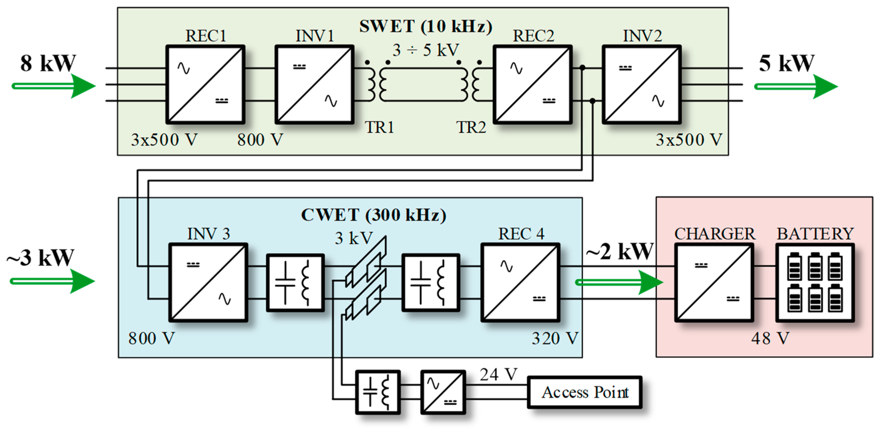
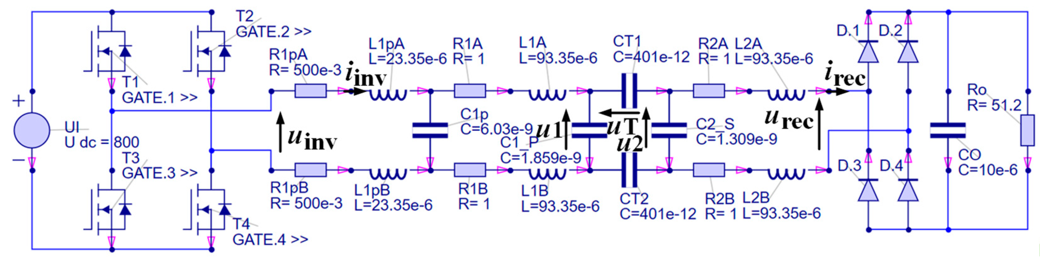
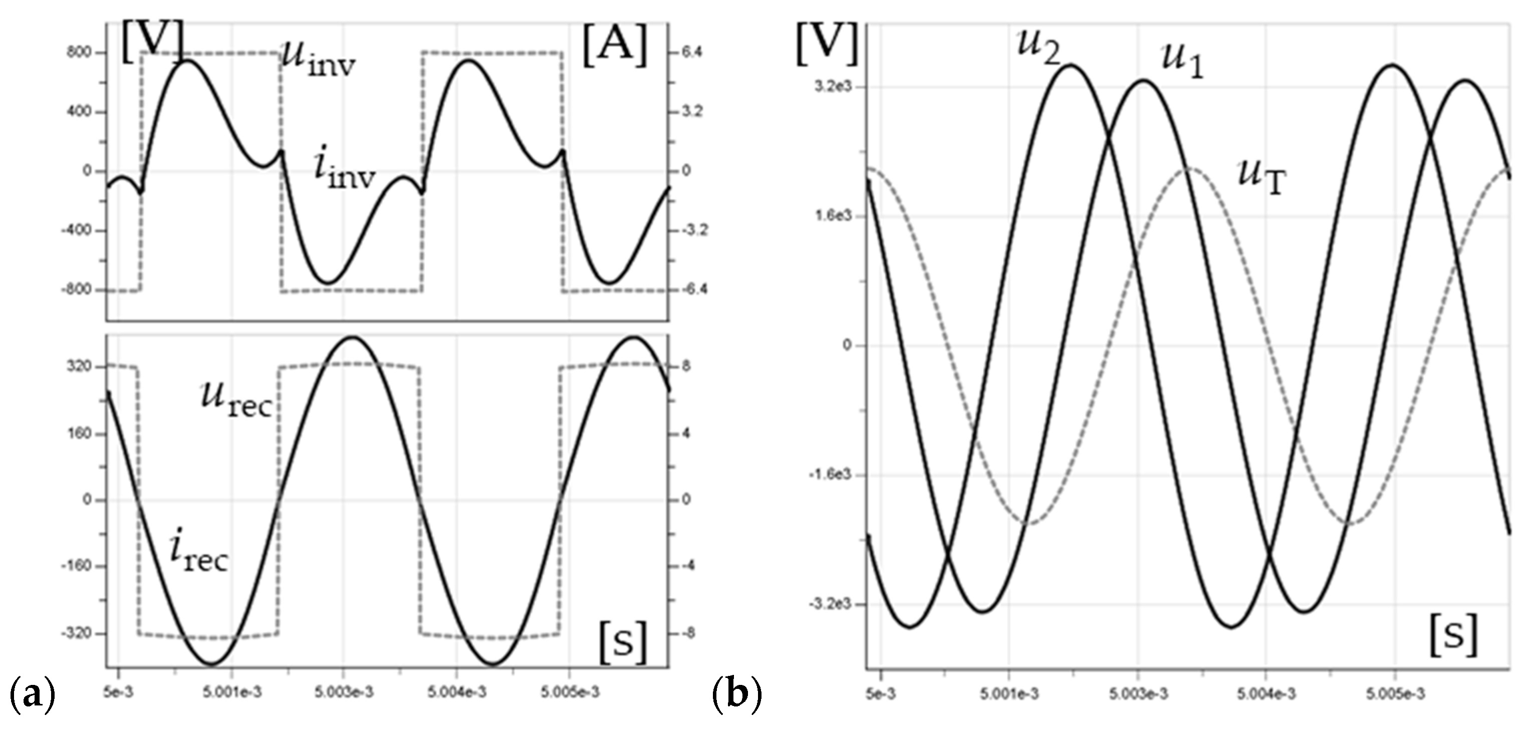
4. The System Model and Simulations

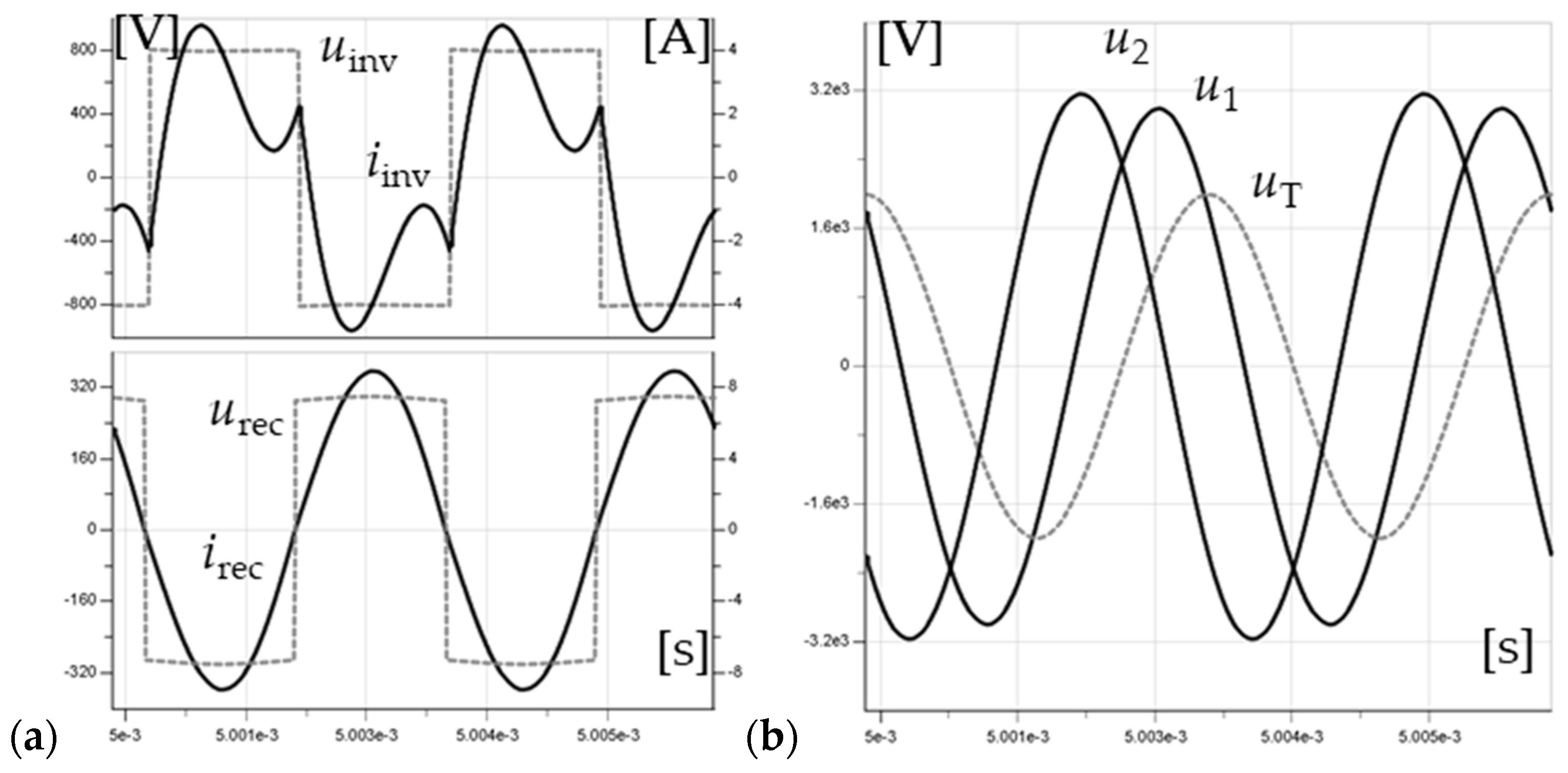
4.1. Simulation Model Setup

A simulation model was developed based on the selected parameters of the LCL-L circuits prepared (Figure 8). This model does not distinguish external capacitors connected to the primary and secondary sides of the capacitive coupler, which form the LCLC-CL topology. Symmetrical pairs of elements are marked with indexes A and B. The resistors in the model represent the approximate power losses in the inductors L1pA, L1pB, L1A, L1B, L2A, L2B. For transistors T1, T2, T3, T4, and diodes D1, D2, D3, D4, a conduction resistance of 0.5 Ω was assumed. The inverter is powered by a constant voltage source of 800 V, with the transistors switched at a frequency of 300 kHz. The rated output voltage is 320 V, and the rated output power is 2 kW, resulting in a load resistance of 51.2 Ω.

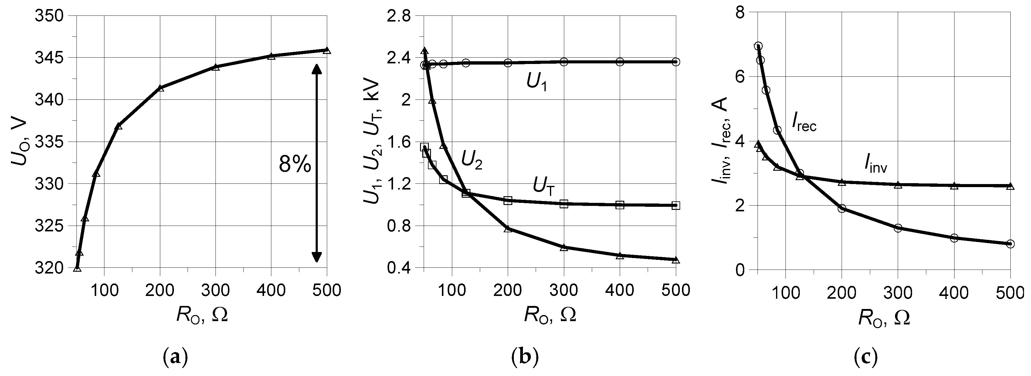
4.2. Key Findings from Simulations

The initial simulation results (Figure 9) illustrate the case with pre-selected parameters for LCL-L circuits as discussed in Section 3 and illustrated in Figure 8. The arrowing of voltages and currents is indicated in the diagrams in Figure 8. The inverter current is noticeably distorted. The amplitudes of the sinusoidal voltages at both the input and output of the capacitive coupler are close to 3.2 kV. However, the output voltage of the system does not reach the expected 320 V, achieving approximately 290 V instead. This discrepancy is caused by the simplified design using the FHA method and the failure to meet condition (5)—k = 3.75. The system efficiency was recorded at 85.4%, with an output power of 1.65 kW. Then, by changing the load resistance while keeping the other parameters constant, the characteristics presented in Figure 10 were determined. With an approximately tenfold increase in load resistance, a fully acceptable system output voltage stiffness of 8% was achieved, changing from 291 V at 51.2 Ω to 314 V at 500 Ω ((314 V–291 V)/291 V = 0.079 ≈ 8%). Increasing the load resistance reduces the voltages on the capacitive coupler, except for the input voltage, and minimizes the inverter and rectifier currents.

4.3. Adjustments to Capacitance and Performance Impact

The simulations revealed that achieving a system output voltage of 320 V, with the desired voltage stiffness, is possible by reducing capacitance C1 or increasing capacitance C1p. These adjustments optimize the performance of the capacitive coupler and ensure a stable voltage gain. The cases of reducing the capacitance C1 (from 1.859 to 1.676 nF) and increasing the capacitance C1p (from 6.03 to 6.54 nF) are illustrated in Figure 11, Figure 12, Figure 13 and Figure 14. An increase in the inverter current is observed without significantly impacting the system efficiency (86.2% and 85.0%, respectively), with an output power of 2 kW. The amplitudes of the sinusoidal voltage at both the input and output of the capacitive coupler are close to 3.2 kV (Figure 11 and Figure 13). The output voltage stiffness (Figure 12 and Figure 14) remains unchanged at 8%. Changes in capacitive coupler voltages as well as inverter and rectifier currents are similar. The system output voltage can be easily adjusted to the required value by correcting the capacitance C1 or C1p. In the constructed CWET system, the capacitance C1 adjustment is implemented due to the use of the variable capacitor at the input of the capacitive coupler.
The last two cases (Figure 15, Figure 16 and Figure 17) demonstrate that maintaining antiphase between the square-wave voltages of the inverter and rectifier is a sufficient condition to ensure acceptable output voltage stiffness of the system. This condition has been consistently met in previous cases (Figure 9, Figure 11 and Figure 13). The capacitance C2 is varied by increasing and decreasing it by 100 pF, with capacitance C1 adjusted accordingly to achieve the target output voltage of 320 V. The phase shift between the inverter and rectifier voltages is noticeable (Figure 15 and Figure 16). As a result, changes in the load resistance significantly degrade the output voltage stiffness (Figure 17). Controlling the antiphase condition between the inverter and rectifier voltages can be accomplished by adjusting the capacitance C2. This enables the desired system output voltage stiffness to be achieved.

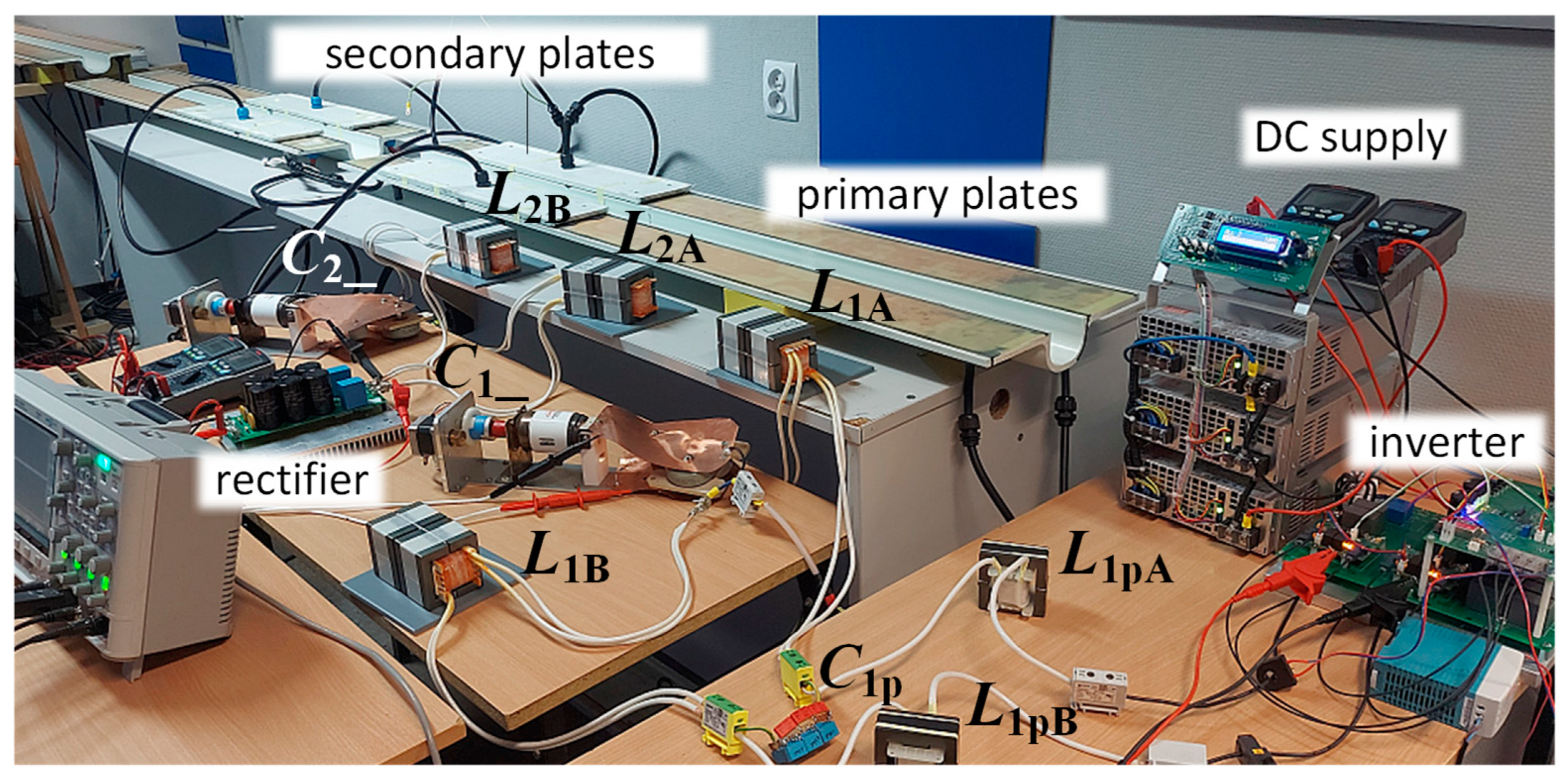
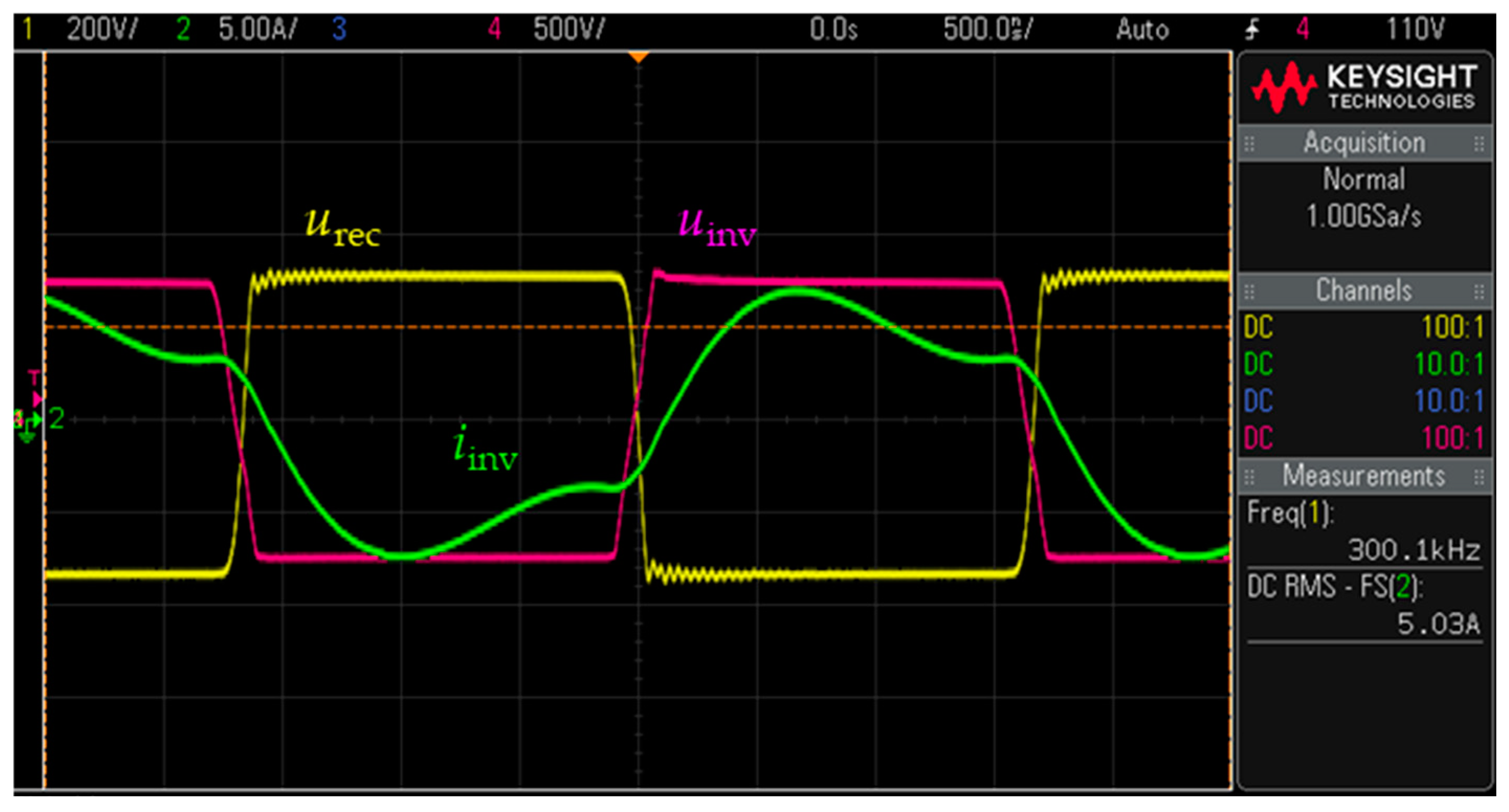
5. Laboratory Verification

The diagram of the constructed CWET system is shown in Figure 18. By connecting additional external capacitors C1_ and C2_ to the input and output of the capacitive coupler, the LCLC-CL topology of matching circuits was achieved. These additional capacitors enable the system to be tuned at start-up to obtain the required output voltage and desired stiffness, as stated in the summary of Section 4.
The primary plate set consists of multiple connected sections that are properly integrated with epoxy caps placed on an epoxy support rail (Figure 19a–c). Movable primary plates are located at the bottom (Figure 19a,c). A suspended monorail equipped with a battery-powered drivetrain travels along the support rail (Figure 19d). The implemented construction solutions were closely linked to the use of the existing mining infrastructure. The standard steel suspended rail was replaced with an epoxy resin rail, meeting all regulatory requirements. The same material was used in the construction of both the primary and secondary plates. The copper tape conductor (10 cm wide) in the plates was shielded by an epoxy glass plate, due to its insulating properties and its electrical strength. The dimensions of the plates, especially the secondary ones, are the result of a compromise between the large surface area of the plates (large capacity of coupling) and the limited length, due to the need to move along the suspended route, including various turns. As part of the HEET II project, the mechanical strength of the composite rail structure was tested to ensure the safety of the tests [22].
During the preliminary stationary laboratory tests of the CWET system prototype, as presented in [21], the plates were positioned upside down. The primary components of the prototype are shown in Figure 20. The primary plate set consisted of only three sections. To increase the capacitive coupling, the secondary plates were doubled, resulting in four plates connected in two pairs. This doubling of plates positively affected the reduction of voltages in the capacitive coupler. The laboratory tests validated the concept and its assumptions, achieving the following parameters under stationary conditions: an operating frequency of 300 kHz, a supply voltage of 779 V, an output voltage of 332 V, an output power of 2045 kW, an efficiency of 88%, an output voltage stiffness of 5%, and RMS input and output voltages of the capacitive coupler at 2.66 and 2.44 kV, respectively [21].

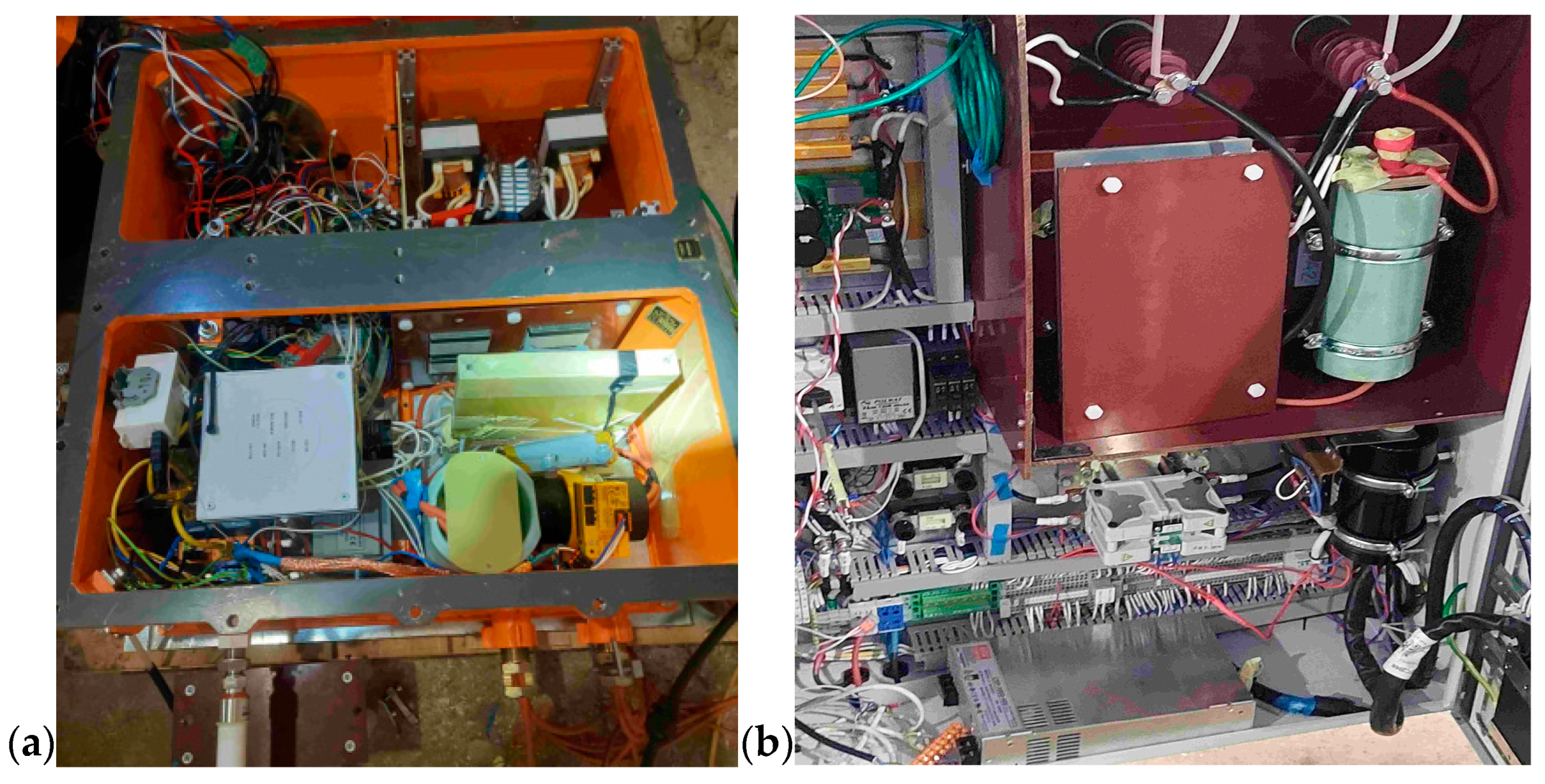
6. In Situ Testing Facility

The actual CWET system was constructed and tested in the “BARBARA” Experimental Mine, located at the −30 m level. The environmental conditions at the test site were as follows: temperature was consistently around 10 °C, and relative humidity ranged from 90% to 100%. A photo of the support rails and a set of 15 sections of primary plates creating a route with a total length of 30 m is shown in Figure 21a. The sections are connected using junction boxes located above the primary plates. In turn, Figure 21b shows the installation of a pair of secondary plates on trolleys that move with the drivetrain. The position of the secondary plates is adjusted and stabilized. These plates transmit electric energy to the battery charger via a coaxial cable to the secondary matching circuit and rectifier.
Based on the previous design calculations (Section 3), and considering the identified parameters (1)–(3) of the capacitive coupler given in Figure 21, the parameters of the system components were selected. The parameters are presented in Table 2 and were measured using the LCR700 LCR bridge produced by Sanwa Electric Instrument Co., Ltd.
The bridge inverter includes CoolSiC MOSFET FF23MR12W1M1P_B11 transistor modules (1200 V, 50 A) produced by Infineon Technologies AG. E65/32/27 ferrite cores made of 3C95 material were used as the cores of the resonant inductors, with an air gap of approximately 1 mm. The windings were made of two parallel strands of the litz wire of the type 650 × 0.1 mm. The capacitance C1p was created by combining PHE448 2000 VDC series of foil capacitors. In turn, the capacitances C1_ and C2_ were formed by high-voltage ceramic disk capacitors with a permissible voltage of 7.5 kV. Each capacitor pack includes an adjustable vacuum capacitor from the CVUN-250AC series, rated at 9 kV with a capacitance of 250 pF. This setup allows for simple and smooth adjustment of the capacitances C1_ and C2_ to achieve the necessary output voltage (C1_ correction) and to ensure the antiphase of the inverter and rectifier voltages—the desired output voltage stiffness (C2_ correction). The DBU-3200-48 module produced by Mean Well Enterprises Co., Ltd. (input: 127–370 V DC, output: max 57.5 V DC, max 55 A DC) was used as a battery charger. Photos of the primary and secondary sides of the CWET system along with their control after being placed in enclosures are shown in Figure 22.
A series of laboratory tests were conducted to verify the operation of the constructed CWET system. The tests included recording selected oscillograms and determining the characteristics. Measurements were taken under stationary conditions and during the movement of a suspended drivetrain with the secondary side of the CWET subsystem. Initially, the CWET system was powered by an adjustable DC power supply and then integrated with the SWET system output (as shown in Figure 2). Measurements were first taken with a resistive load on the output rectifier. Subsequently, a charger with a set of charged batteries was connected as a load. The drivetrain suspended on a composite rail with the secondary side of the CWET subsystem is shown in Figure 23.

7. Initial Startup and Tuning the CWET System

The integration of the CWET system at the laboratory test stand began with the tuning of resonance parameters in the matching circuits. This was achieved using high-voltage adjustable capacitors connected to the input and output of the capacitive coupler. The tuning process followed the recommendations outlined in the summary of Section 4, resulting in the desired output voltage of approximately 320 V and high output voltage stiffness. This was accomplished by adjusting the input and output capacitances of the capacitive coupler. An example recorded oscillogram is shown in Figure 24, illustrating the antiphase condition of the rectangular voltages between the inverter and rectifier. During startup, the CWET system was powered by an adjustable laboratory power source of 750 V and included a limited number of primary plates (eight pieces). The load consisted of a set of power resistors with possible resistances of {36, 54, 72, ∞} Ω. At the lowest load resistance, the CWET system achieved its highest output power of 3 kW with an efficiency of 75%.
Then, voltage and current measurements were conducted on the primary side of the CWET system under stationary conditions. The voltages and currents of the power supply inverter and the primary plates were recorded (Figure 25). The inverter voltages were in the range of 2.05–2.25 kV RMS, with 2.25 kV at no load. The voltage and current waveforms for the primary plates are sinusoidal, whereas the inverter current waveform is non-sinusoidal and significantly dependent on the load.
On the secondary side of the CWET system, sinusoidal voltage and current waveforms were observed directly at the output of the capacitive coupler. An increase in load resistance resulted in a decrease in voltage and current, with their initial values not exceeding 3 kV and 9 A RMS, respectively. Despite changes in load resistance, an 8% output voltage stiffness of the CWET system was achieved.
In a capacitive energy transfer system, it is crucial to maintain a suitable (uniform and low) distance between the primary and secondary plates. This ensures a high capacitive coupling required for efficient CWET operation. Therefore, time was taken to adjust this distance under stationary conditions, and then the behaviour of the secondary plates was monitored while travelling along the route.
In the next step, the load of the CWET system under stationary conditions was followed by a run along the suspended track, during which the system operated with reduced voltage. The output voltage waveforms of the CWET system at the resistance load were recorded, with an example shown in Figure 26. Significant voltage reductions can occur when the secondary plates pass through gaps in the primary plates, particularly at the chain suspension points. In the example, the voltage reduction occurs from about 144 V to around 30 V. The second effect observed in Figure 26 is voltage instability during energy transmission, along with the voltage peaks, such as a peak of 158 V in the example. This can be dangerous for the charging system. It has been noted that this is caused by the excessive proximity of the secondary plates to the primary plates, particularly at the point where the rails join, where the small wheels of the receiving trolley fall into the gaps between the suspended rails. These problems were significantly limited in the final version of the CWET system by modifying and extending the primary plates.

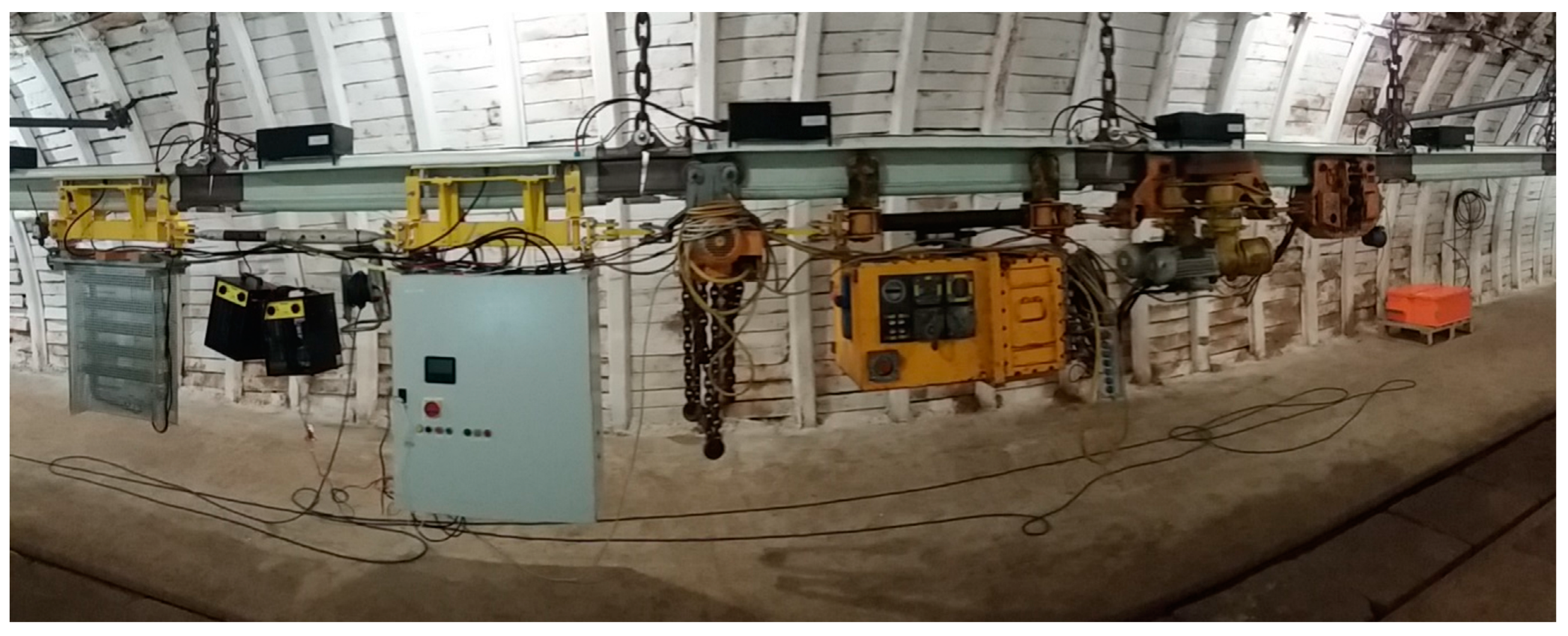
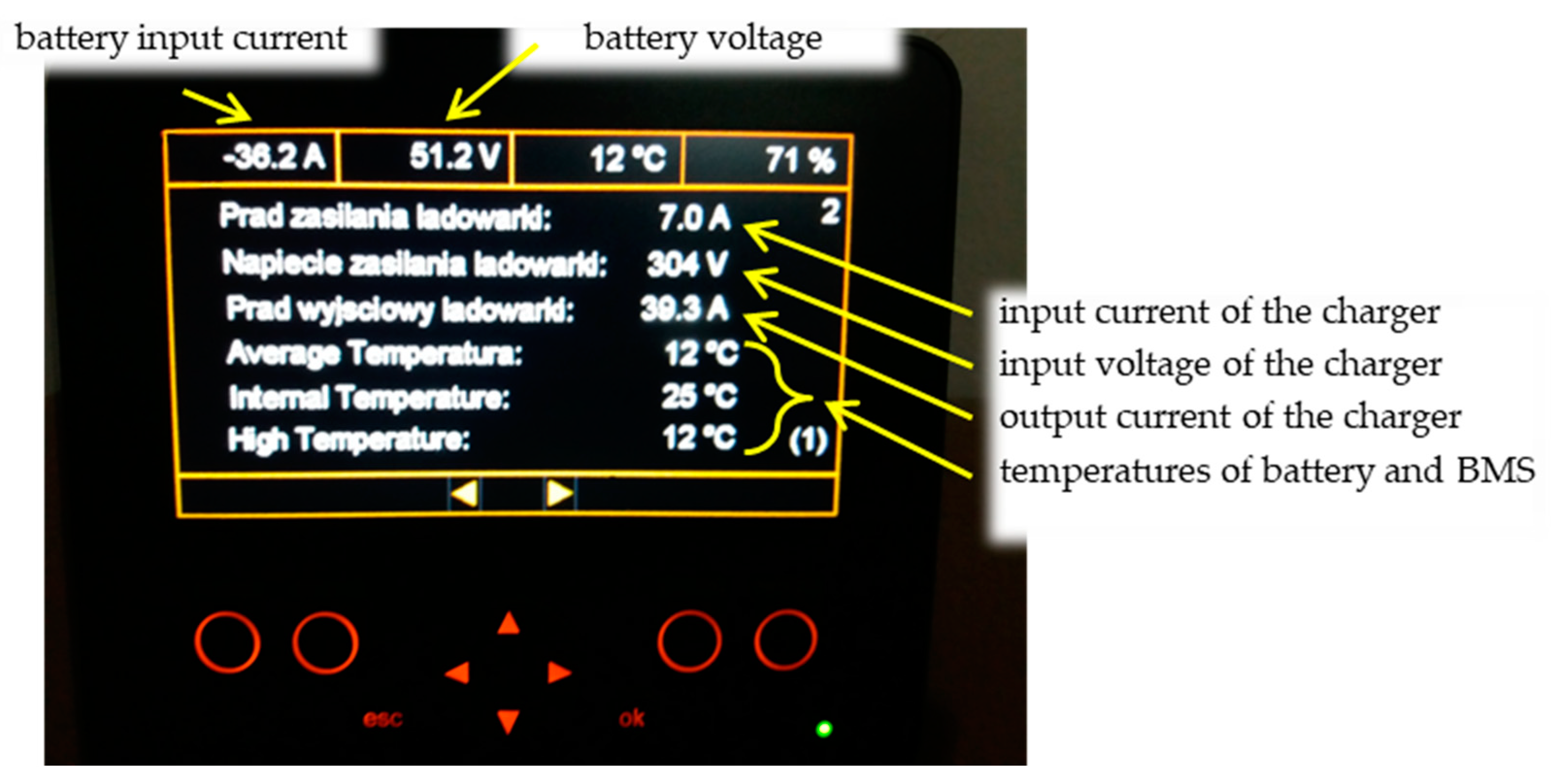
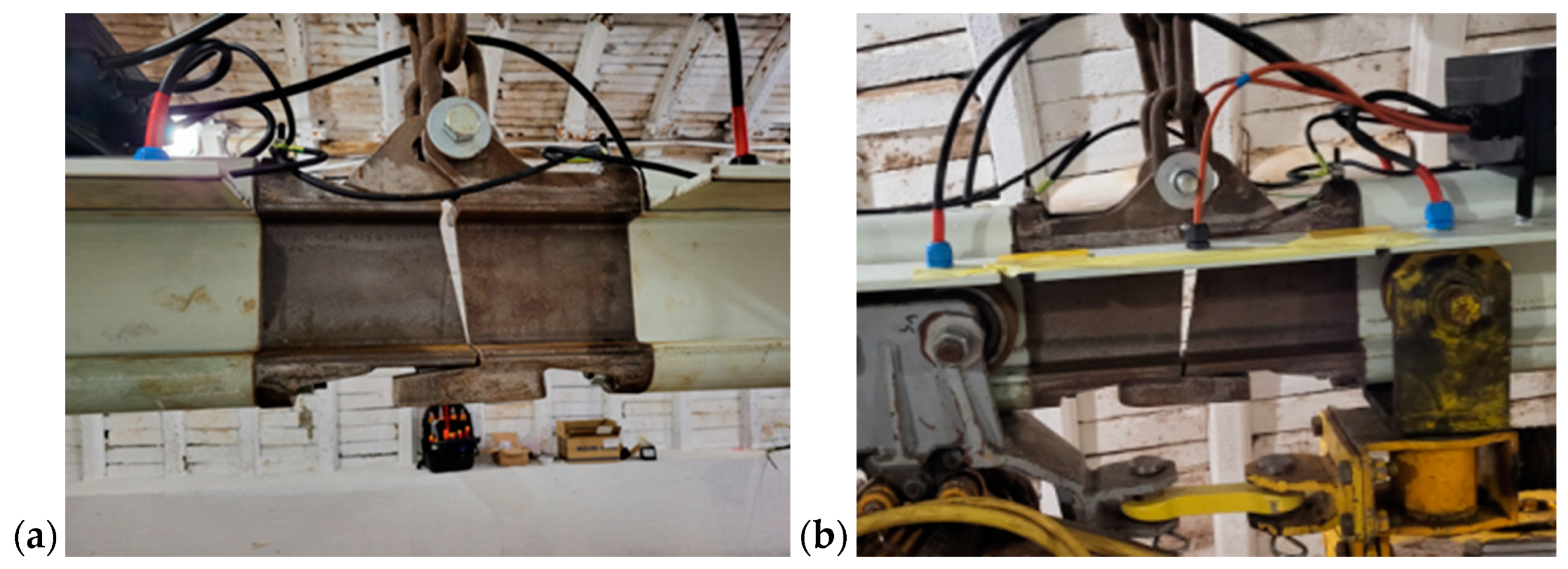
8. Integration of the CWET System and the Drivetrain

8.1. Integration and Initial Testing

Once the operation of the CWET system with a resistive load was confirmed and the output voltage at the CWET receiver was suitable for the battery charger, the next integration step was realized. The charger was connected to the rectifier output, and the CWET system was started under stationary conditions. The charging process was initiated, gradually increasing the output current until the charger’s output power reached 2 kW. An example parameters screen during charger operation with an output power of 2 kW (39.3 A × 51.2 V = 2012 W) is shown in Figure 27.

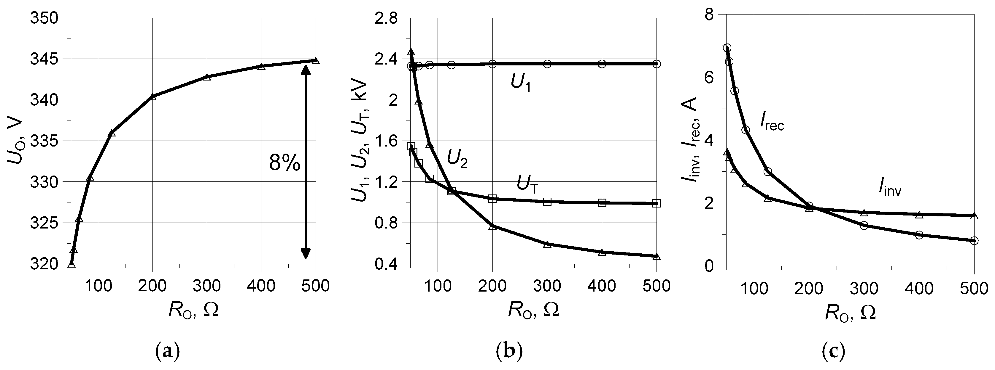
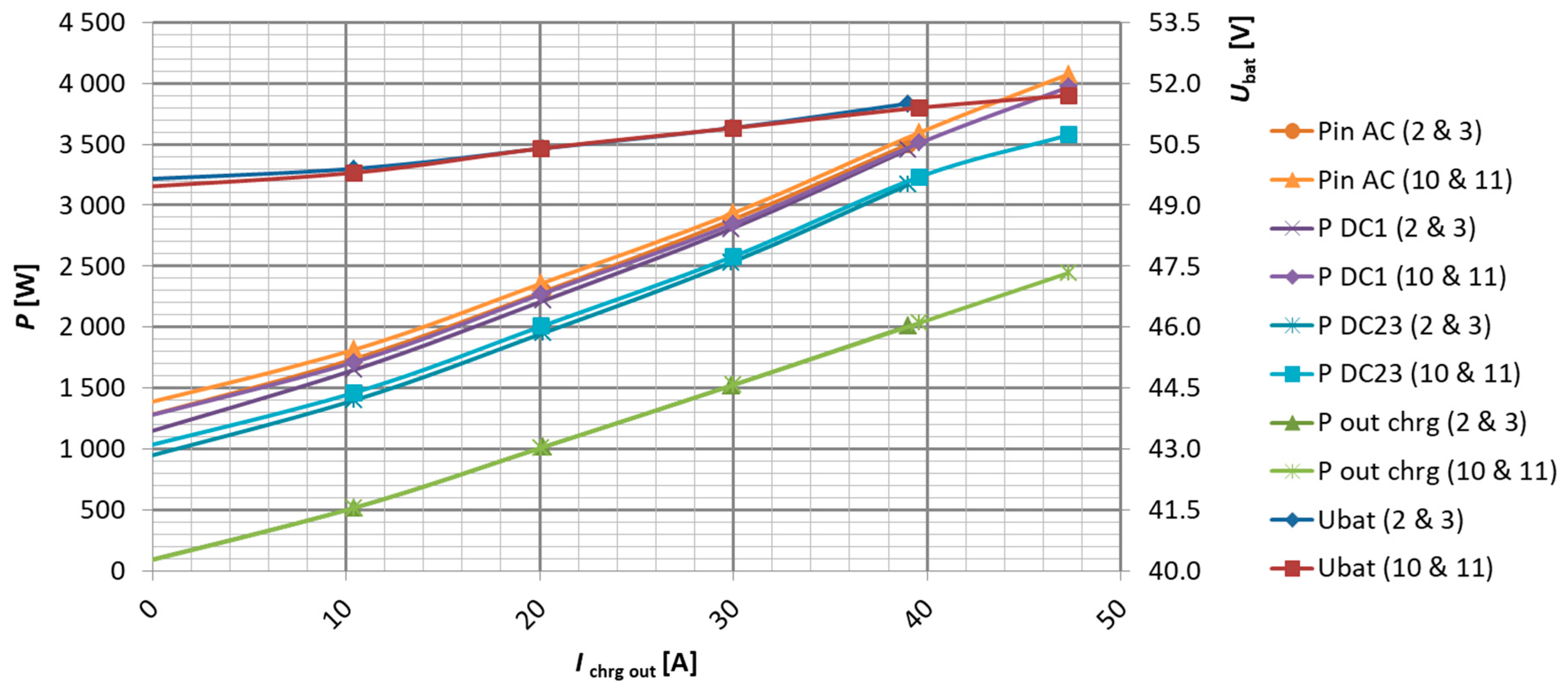
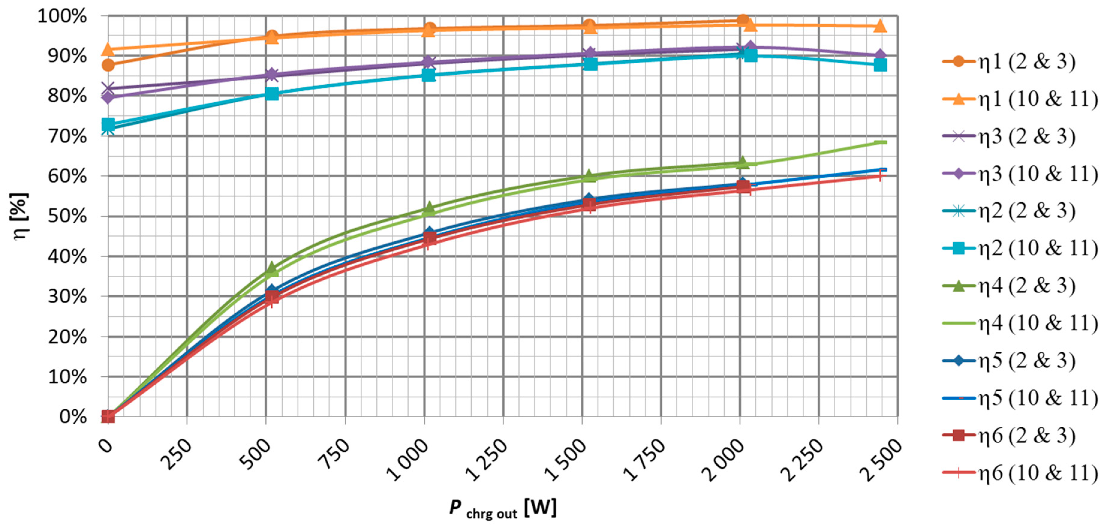
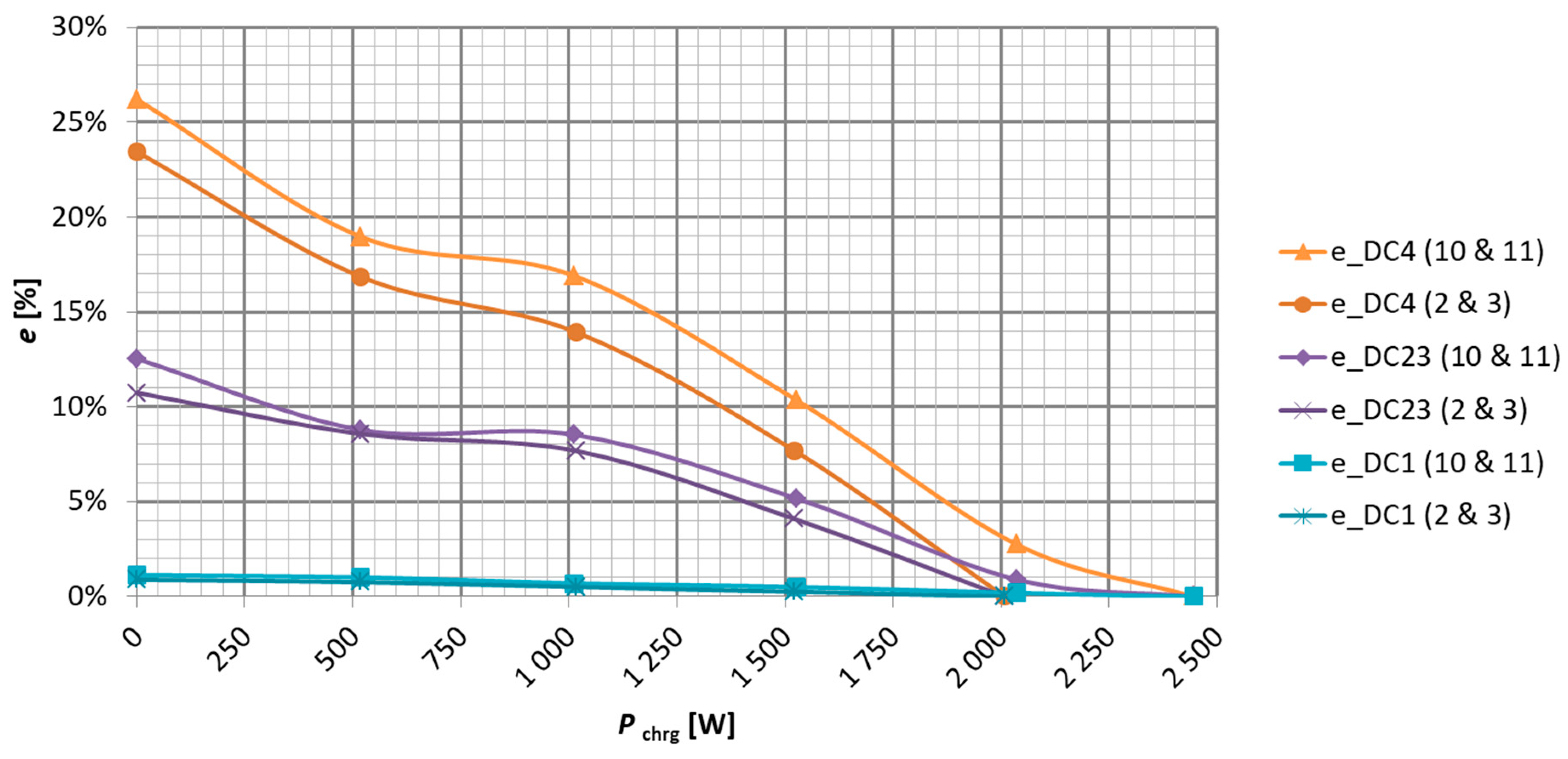
8.2. Stationary Measurements and Key Observations

Stationary measurements of voltages and currents were carried out for various positions of the primary plates as a function of the charger’s output current. The primary side of the CWET system was powered by the SWET system (Figure 2), with the charger and a battery connected to its secondary side. Additionally, three Access Point modules were wirelessly powered (Figure 2). The CWET system included 15 primary plate sections (30 m). Measurements were taken in two locations along the suspended route; secondary plates were located under primary plates No. 2 and 3, and then No. 10 and 11, counting from the side of the powered primary plates. Based on the measurements, the power, efficiency, and the output voltage stiffness were calculated (Figure 28, Figure 29 and Figure 30). The following markings were adopted (referring to Figure 2): PinAC—the input power of the rectifier (REC1) in the SWET system, PDC1—the input power of the inverter (INV1) in the SWET system, PDC23—the input power of the inverter (INV3) in the CWET system, Pout chrg—the output power of the charger, and Ubat—the battery voltage. In one case, the output power of the charger was approximately 2.5 kW, while the power drawn from the mains was 4 kW.
In Figure 29, the efficiency characteristics are presented with the following notations:
-
η1 = PDC1/PAC·100%,
-
η2 = PDC23/PDC1·100%,
-
η3 = PDC23/PAC·100%,
-
η4 = Pout chrg/PDC23·100%,
-
η5 = Pout chrg/PDC1·100%,
-
η6 = Pout chrg/PAC·100%.
Efficiencies for various drivetrain positions were calculated as the charging power increased. The SWET system demonstrates high efficiency (η1, η2, η3), while the CWET system shows lower efficiency. Total transmission efficiency (SWET + CWET) reached approximately 60% at a charging power of 2 kW. In this case, the CWET system efficiency was 63%. The relatively low efficiency observed during the measurements is influenced by powering additional low-power receivers (approximately 3 × (25–30 W)) and the protection of the secondary side of the CWET system by a resistive voltage limiter (power consumption approximately 100 W). Furthermore, the configuration of the selected matching circuits, especially on the primary side of the CWET system, forces relatively large currents. Electrical connections involving relatively long cables, as well as power losses in the dielectrics of these cables and the supporting structure of the CWET system, are significant sources of power losses.
The output voltages stiffness characteristics of the SWET and CWET systems are shown in Figure 30. According to Figure 2, case DC1 corresponds to the input voltage of the inverter (INV1) in the SWET system, case DC23 relates to the input voltage of the inverter (INV3) in the CWET system, and case DC4 corresponds to the changes in the supply voltage of the charger. Each time, the reference voltage is set at the level of the highest charging power. For obvious reasons, the resulting stiffness is lowest at the output of the CWET system, reaching approximately 25%, which indicates a 25% increase in this voltage without charging. It should be noted that the SWET system significantly negatively affects this outcome. Subsequent tests revealed that the output voltage stiffness obtained was acceptable for the proper operation of the system.

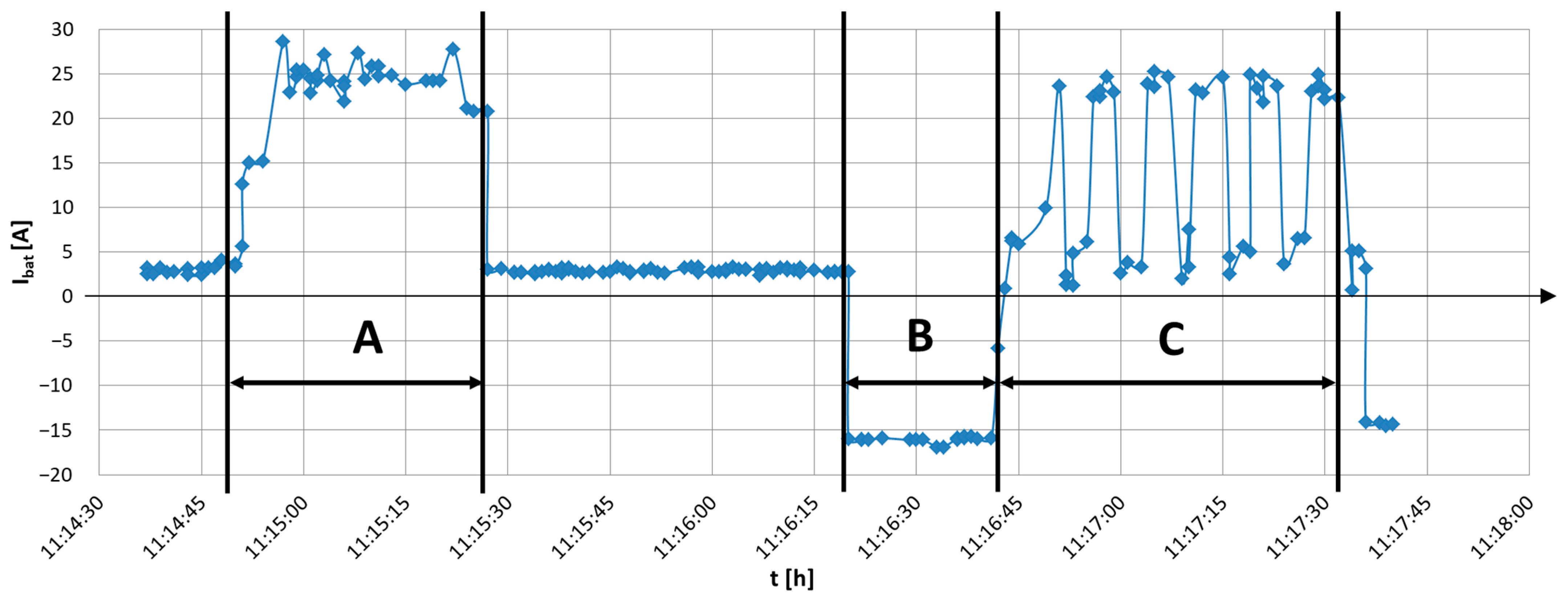
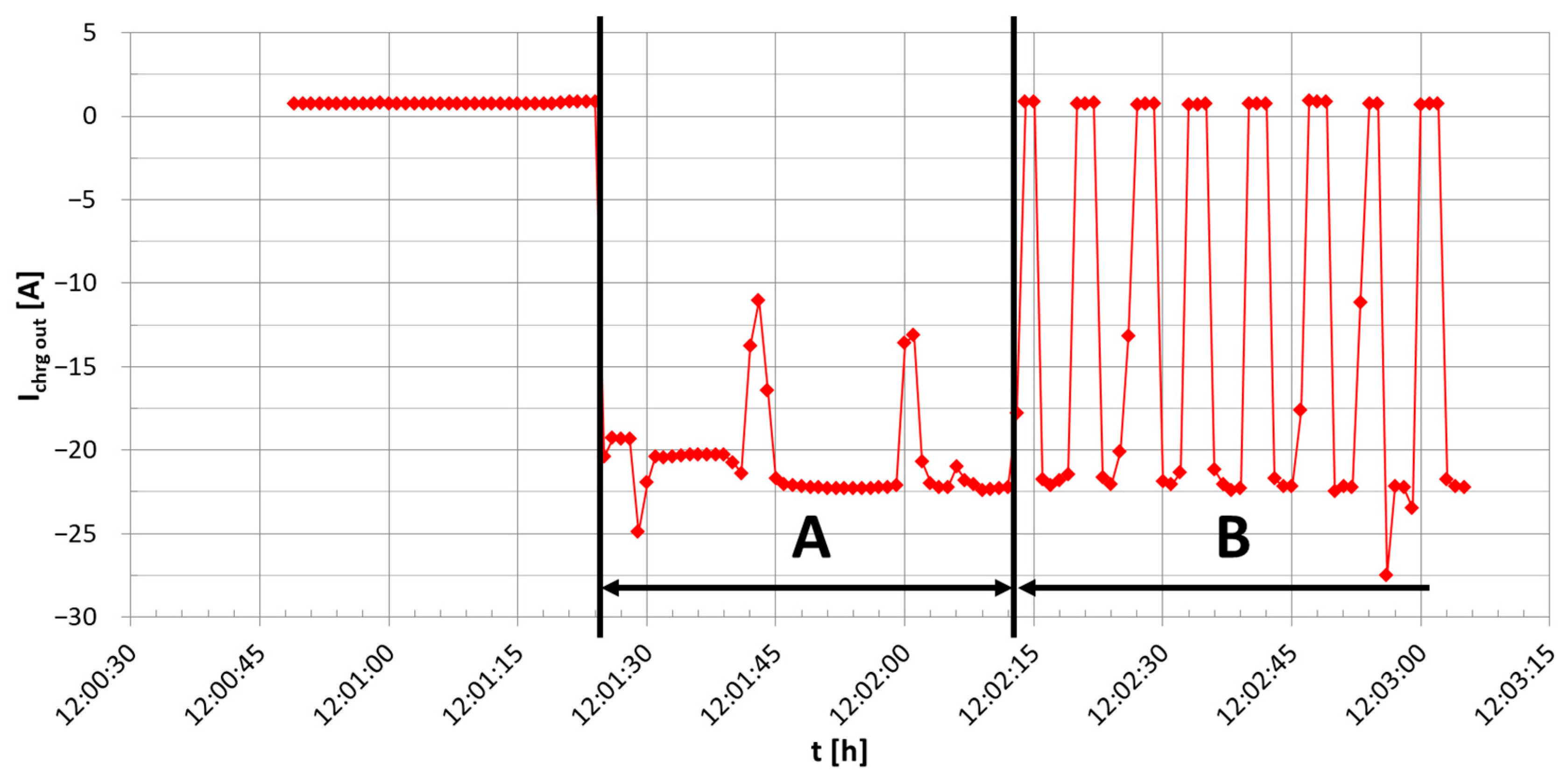
8.3. Dynamic Measurements and Key Observations

The next stage of the laboratory tests involved evaluating the charging via the CWET system during drivetrain movement along the route. Figure 31 compares the battery current during two runs, as recorded by the Battery Management System (BMS) configuration software (version 2.1.33). Positive current values indicate battery discharge, while negative values indicate charging. Initially, the CWET system was inactive (section A), and an average current of about 25 A was drawn from the battery while the drivetrain was moving. Subsequently, the drivetrain was parked, and the CWET system was activated with an output power of 1 kW. The charger output current was about 20 A, with around 17 A used for charging the battery and 3 A consumed by the control system (section B). When the drivetrain began moving again (section C), it was observed that when the secondary plates are positioned beneath the primary plates, energy is transferred by the CWET system, causing the current drawn from the battery to decrease to approximately 5 A. However, the operation is not continuous during travel due to gaps between the primary plates, as explained further in the next part. Nevertheless, the CWET system effectively reduces the current drawn from the battery (comparing section C to section A), thereby extending the operating time when powered by the battery.
During the next test, the charger supply voltage and output current were observed. An example of the recorded waveforms, with the charger output power at approximately 2 kW, is shown in Figure 32. When the secondary plates move through gaps in the primary plates (Figure 33a), the charger supply voltage decreases, interrupting the charging process. This issue was resolved and the charging time extended by reducing these gaps through the introduction of additional, shorter primary plates (Figure 33b). The effectiveness of this solution is confirmed by the measured output current of the CWET system (Figure 34). Positive current indicates battery discharge related to powering the secondary CWET control system, while negative current corresponds to energy transmission. Only a temporary change in the output current of the CWET system is noticeable when passing through the connection points of the support rails (A), and energy transmission is not interrupted, unlike when passing through the connection points without additional primary plates (B).

9. Conclusions

Laboratory verification of the simplified prototype under stationary conditions (primary plates consisted of only three sections) confirmed that the desired properties were obtained. At an operating frequency of 300 kHz, the output power was 2045 W, the efficiency was 88%, and the output voltage stiffness was better than 5% even with a tenfold increase in load resistance compared to the nominal value.
The design methods for the LCLC-CL matching circuits and the identification of capacitive coupler parameters were adapted and applied. It was demonstrated that adjusting the input capacitance of the capacitive coupler is sufficient to modify the output voltage. However, to achieve the desired output voltage stiffness, the antiphase condition of the inverter and rectifier voltages must be met.
The in situ verification process included the integration of various subsystems at an underground test station in the Barbara Experimental Mine. This task involved the mechanical and electrical integration of the SWET and CWET systems, along with the drivetrain. The power transmission function was started in steps, increasing the level of integration. Initially, resistors were used as the load for the CWET system, which was later replaced by a battery charger as the target load. During the operation, necessary adjustments were made to the resonant circuits and control software. They focused on selecting the appropriate input and output capacitances for the capacitive coupler to ensure the required output voltage and its stiffness. Necessary tuning of the charger’s parameters (like under the voltage threshold level or the limitation of charging current depending on the available voltage of the charger supply) was also performed to enhance its effectiveness. Successful energy transmission through the SWET and CWET systems, as well as the possibility of charging the drivetrain battery, were confirmed.
Acceptable system parameters were achieved, with wireless energy transmission to the suspended drivetrain reaching up to approximately 2 kW. The total efficiency of the connected systems was around 60%, both in stationary conditions and during movement.
The primary focus of future research will be on reducing power losses, improving system efficiency, and modifying the long primary plates. This modification will involve fully integrating additional short primary plates with them to ensure continuous energy transmission during any movement of the secondary plates.

Author Contributions

Conceptualization, M.S. and Z.K.; methodology, M.S., M.K. and Z.K.; software, S.J. and K.P.; validation, S.J., M.S. and Z.K.; formal analysis, M.S. and J.R.-R.; investigation, M.S., Z.K., S.J., P.L. and K.P.; resources, M.S., S.J., Z.K., P.L. and J.R.-R.; data curation, M.S. and Z.K.; writing—original draft preparation, M.S. and Z.K.; writing—review and editing, M.K., Z.K., B.P. and K.S.; visualization, M.S., Z.K., S.J. and J.R.-R.; project administration, M.K., B.P. and K.S.; funding acquisition, M.K., K.S. and B.P. All authors have read and agreed to the published version of the manuscript.

Funding

  • Scientific paper published as part of an international project co-financed by the European Commission Research Fund for Coal and Steel (RFCS) in the years 2020–2023; grant agreement no: 899469.
Energies 18 00521 g035
  • Scientific paper published as part of an international project co-financed by the Ministry of Science and Higher Education’s program “PMW” in the years 2020–2023; contract no. 5117/FBWiS/2020/2.
  • Scientific paper published as part of an international project co-financed by the Ministry of Science and Higher Education’s program “PMW” in the years 2020–2023; contract no. 5122/FBWiS/2020/2.

Data Availability Statement

The original contributions presented in the study are included in the article, further inquiries can be directed to the corresponding author.

Conflicts of Interest

Author Marcin Skóra, Joanna Rogala-Rojek, Sebastian Jendrysik, Krzysztof Stankiewicz, and Bartosz Polnik were employed by the company KOMAG Institute of Mining Technology. The remaining authors declare that the research was conducted in the absence of any commercial or financial relationships that could be construed as a potential conflict of interest.

References

  1. Dai, J.; Ludois, D. A survey of wireless power transfer and a critical comparison of inductive and capacitive coupling for small gap applications. IEEE Trans. Power Electron. 2015, 30, 6017–6029. [Google Scholar] [CrossRef]
  2. Lecluyse, C.; Minnaert, B.; Kleemann, M. A Review of the Current State of Technology of Capacitive Wireless Power Transfer. Energies 2021, 14, 5862. [Google Scholar] [CrossRef]
  3. Pahlavan, S.; Shooshtari, M.; Jafarabadi Ashtiani, S. Star-Shaped Coils in the Transmitter Array for Receiver Rotation Tolerance in Free-Moving Wireless Power Transfer Applications. Energies 2022, 15, 8643. [Google Scholar] [CrossRef]
  4. Detka, K.; Górecki, K. Wireless Power Transfer—A Review. Energies 2022, 15, 7236. [Google Scholar] [CrossRef]
  5. Luo, B.; Long, T.; Guo, L.; Dai, R.; Mai, R.; He, Z. Analysis and Design of Inductive and Capacitive Hybrid Wireless Power Transfer System for Railway Application. IEEE Trans. Ind. Appl. 2020, 56, 3034–3042. [Google Scholar] [CrossRef]
  6. Vincent, D.; Huynh, P.S.; Williamson, S.S. A Link-Independent Hybrid Inductive and Capacitive Wireless Power Transfer System for Autonomous Mobility. IEEE J. Emerg. Sel. Top. Ind. Electron. 2022, 3, 211–218. [Google Scholar] [CrossRef]
  7. Karagozler, M.E.; Goldstein, S.C.; Ricketts, D.S. Analysis and modeling of capacitive power transfer in microsystems. IEEE Trans. Circuit Syst. I 2012, 59, 1557–1566. [Google Scholar] [CrossRef]
  8. Hui SY, R.; Ho WW, C. A new generation of universal contactless battery charging platform for portable consumer electronic equipment. IEEE Trans. Power Electron. 2005, 20, 620–627. [Google Scholar]
  9. Kaczmarczyk, Z.; Kasprzak, M.; Ruszczyk, A.; Sowa, K.; Zimoch, P.; Przybyła, K.; Kierepka, K. Inductive Power Transfer Subsystem for Integrated Motor Drive. Energies 2021, 14, 1412. [Google Scholar] [CrossRef]
  10. Hu, A.P.; Liu, C.; Li, H.L. A Novel Contactless Battery Charging System for Soccer Playing Robot. In Proceedings of the 15th International Conference on Mechatronics and Machine Vision in Practice, Auckland, New Zealand, 2–4 December 2008; pp. 646–650. [Google Scholar]
  11. Lu, F.; Zhang, H.; Hofmann, H.; Mi, C. A double-sided LCLC-compensated capacitive power transfer system for electric vehicle charging. IEEE Trans. Power Electron. 2015, 30, 6011–6014. [Google Scholar] [CrossRef]
  12. Zhang, H.; Lu, F.; Hofmann, H.; Liu, W.; Mi, C. A four-plate compact capacitive coupler design and LCL-compensated topology for capacitive power transfer in electric vehicle charging application. IEEE Trans. Power Electron. 2016, 31, 8541–8551. [Google Scholar]
  13. Lu, F.; Zhang, H.; Mi, C. A two-plate capacitive wireless power transfer system for electric vehicle charging applications. IEEE Trans. Power Electron. 2018, 33, 964–969. [Google Scholar] [CrossRef]
  14. Sinha, S.; Kumar, A.; Regensburger, B.; Afridi, K.K. A new design approach to mitigating the effect of parasitics in capacitive wireless power transfer systems for electric vehicle charging. IEEE Trans. Transp. Electrific. 2019, 5, 1040–1059. [Google Scholar] [CrossRef]
  15. Vu, V.-B.; Dahidah, M.; Pickert, V.; Phan, V.-T. An Improved LCL-L Compensation Topology for Capacitive Power Transfer in Electric Vehicle Charging. IEEE Access 2020, 8, 27757–27768. [Google Scholar] [CrossRef]
  16. Panchal, C.; Stegen, S.; Lu, J. Review of static and dynamic wireless electric vehicle charging system. Eng. Sci. Technol., Int. J. 2018, 21, 922–937. [Google Scholar] [CrossRef]
  17. Deja, P.; Skóra, M.; Stankiewicz, K.; Tokarczyk, J.; Kasprzak, M.; Kaczmarczyk, Z.; Hildebrandt, R. Wireless energy transfer system for use in underground mining. Acta Montan. Slovaca 2022, 27, 267–280. [Google Scholar]
  18. Erel, M.Z.; Bayindir, K.C.; Aydemir, M.T.; Chaudhary, S.K.; Guerrero, J.M. A comprehensive review on wireless capacitive power transfer technology: Fundamentals and applications. IEEE Access 2022, 10, 3116–3143. [Google Scholar] [CrossRef]
  19. Gierlotka, S. Elektropatologia porażenia prądem elektrycznym oraz bezpieczeństwo przy urządzeniach elektrycznych (Electropathology of electric shock and the safety of using electrical equipment). In Zeszyty dla Elektryków; Booklets for Electricians—No. 12; Grupa Medium: Warsaw, Poland, 2015; ISBN 978-83-64094-43-9. [Google Scholar]
  20. Lu, F.; Zhang, H.; Hofmann, H.; Mi, C. A double-sided LC-compensation circuit for loosely coupled capacitive power transfer. IEEE Trans. Power Electron. 2018, 33, 1633–1643. [Google Scholar] [CrossRef]
  21. Kaczmarczyk, Z.; Kasprzak, M.; Lasek, P.; Przybyła, K.; Skóra, M.; Stankiewicz, K. Realizacja systemu bezprzewodowego przesyła energii na zasadzie sprzężenia pojemnościowego/Implementation of a wireless energy transfer system based on capacitive coupling. In Proceedings of the 16th Conference Control in Power Electronics and Electric Drives—“SENE 2023”, Łódź, Poland, 22–24 November 2023. [Google Scholar]
  22. Pytlik, A.; Hildebrandt, R.; Stankiewicz, K.; Skóra, M. Suspended mining monorail composite-steel rail resistance to static and fatigue loads. Arch. Min. Sci. 2024, 69, 509–528. [Google Scholar] [CrossRef]
Figure 1. A general diagram of the CWET system (upper) and a simplified diagram for the FHA method (bottom).
Energies 18 00521 g001
Figure 2. The integration of the SWET (10 kHz) and CWET (300 kHz) systems: power flow and operational interconnection.
Energies 18 00521 g002
Figure 3. Illustrative view of the set of plates forming the capacitive coupler (dimensions in centimeters; no scale).
Energies 18 00521 g003
Figure 4. Inter-plate and ground capacitances of the capacitive coupler, along with those of the inverter and rectifier.
Energies 18 00521 g004
Figure 5. Equivalent diagrams of the capacitive coupler: (a) simplified, (b) simplified for the FHA method (CM = CT/2, C1 = CP + CT/2, C2 = CS + CT/2).
Energies 18 00521 g005
Figure 6. Measuring systems—method of identifying the capacitive coupler parameters.
Energies 18 00521 g006
Figure 7. Diagram referring to LCL-L topology.
Energies 18 00521 g007
Figure 8. Model of CWET system—GeckoCIRCUITS.
Energies 18 00521 g008
Figure 9. Simulation results: (a) voltages and currents of the inverter and rectifier (uinv, iinv, urec, irec) and (b) voltages of the capacitive coupler (u1, u2, uT) for the selected parameters of the system (400 V/div; 2 A/div; 160 V/div; 4 A/div; 1.6 kV/div).
Energies 18 00521 g009
Figure 10. Determined characteristics: (a) output voltage UO, (b) RMS voltages of the capacitive coupler U1, U2, UT, and (c) RMS currents of the inverter Iinv and rectifier Irec for the selected parameters of the system as a function of the load resistance RO.
Energies 18 00521 g010
Figure 11. Simulation results: (a) voltages and currents of the inverter and rectifier (uinv, iinv, urec, irec) and (b) voltages of the capacitive coupler (u1, u2, uT) for the reduced capacitance C1 = 1.676 nF (400 V/div; 2.4 A/div; 160 V/div; 4 A/div; 1.6 kV/div).
Energies 18 00521 g011
Figure 12. Determined characteristics: (a) output voltage UO, (b) RMS voltages of the capacitive coupler U1, U2, UT, and (c) RMS currents of Iinv inverter and Irec rectifier for the reduced capacitance C1 = 1.676 nF as a function of the load resistance RO.
Energies 18 00521 g012
Figure 13. Simulation results: (a) voltages and currents of the inverter and rectifier (uinv, iinv, urec, irec) and (b) voltages of the capacitive coupler (u1, u2, uT) for the increased capacitance C1p = 6.54 nF (400 V/div; 2.4 A/div; 160 V/div; 4A/div; 1.6 kV/div).
Energies 18 00521 g013
Figure 14. Determined characteristics: (a) output voltage UO, (b) RMS voltages of the capacitive coupler U1, U2, UT, and (c) RMS currents of Iinv inverter and Irec rectifier for the increased capacitance C1p = 6.54 nF as a function of the load resistance RO.
Energies 18 00521 g014
Figure 15. Simulation results: (a) voltages and currents of the inverter and rectifier (uinv, iinv, urec, irec) and (b) voltages of the capacitive coupler (u1, u2, uT) for the corrected capacitances C1 = 1.429 nF and C2 = 1.409 nF (400 V/div; 6 A/div; 160 V/div; 4 A/div; 1.6 kV/div).
Energies 18 00521 g015
Figure 16. Simulation results: (a) voltages and currents of the inverter and rectifier (uinv, iinv, urec, irec) and (b) voltages of the capacitive coupler (u1, u2, uT) for the corrected capacitances C1 = 1.481 nF and C2 = 1.209 nF (400 V/div; 3.2 A/div; 160 V/div; 4A/div; 1.6 kV/div).
Energies 18 00521 g016
Figure 17. Determined characteristics of output voltage UO for the corrected capacitances C1 = 1.429 nF, C2 = 1.409 nF (UO,C1+) and C1 = 1.481 nF, C2 = 1.209 nF (UO,C1−) as a function of the load resistance RO.
Energies 18 00521 g017
Figure 18. Diagram of CWET system.
Energies 18 00521 g018
Figure 19. Illustration of the support rail and plates design: (a) simplified cross-section, (b) photo, (c) view of the primary and secondary plates, and (d) method of suspending the drivetrain.
Energies 18 00521 g019
Figure 20. Photo of the CWET system prototype during laboratory tests.
Energies 18 00521 g020
Figure 21. Photos of the constructed CWET system: (a) suspended support rail with a set of primary plates, (b) two suspended trolleys with two pairs of secondary plates.
Energies 18 00521 g021
Figure 22. Photos of enclosures: (a) inverter and the primary matching circuit, (b) secondary matching circuit, the rectifier, and the charger.
Energies 18 00521 g022
Figure 23. The drivetrain and secondary side of the CWET subsystem suspended on the composite rail.
Energies 18 00521 g023
Figure 24. Sample waveforms from tuning the CWET system.
Energies 18 00521 g024
Figure 25. Waveforms characterizing the CWET system, i.e., voltage (CH1, yellow) and current (CH2, green) of the inverter, voltage (CH4, magenta) and current (CH3, blue) supplying the primary plates depending on load as follows: (a) Ro = 36 Ω, (b) Ro = 54 Ω, (c) Ro = 72 Ω, (d) Ro → ∞.
Energies 18 00521 g025
Figure 26. Example of voltage waveform on a resistive load during monorail travel (20 V/div).
Energies 18 00521 g026
Figure 27. Diagnostic screen displaying CWET system parameters, including current, voltage, and temperature values.
Energies 18 00521 g027
Figure 28. Power and voltage characteristics depending on the charger output current.
Energies 18 00521 g028
Figure 29. Efficiency characteristics depending on the charger output power.
Energies 18 00521 g029
Figure 30. Output voltage stiffness characteristics depending on the charger output power.
Energies 18 00521 g030
Figure 31. Comparison of the battery current: driving without the CWET system (A), charging with the CWET system while drivetrain is parked (B), and driving with the CWET system (C).
Energies 18 00521 g031
Figure 32. Waveforms of the charger supply voltage (CH1, red, 50 V/div) and the charger output current (CH2, blue, 10 A/div) during travelling.
Energies 18 00521 g032
Figure 33. View of the rail connection: (a) with a gap, and (b) after the installation of additional primary plates.
Energies 18 00521 g033
Figure 34. Waveform of the output current of the CWET system while travelling with additional primary plates (A) and without them (B).
Energies 18 00521 g034
Table 1. Capacitances measured as shown in Figure 6.
CapacitanceValue [pF]
CC1755
CE1656
CF2460
Table 2. Measured CWET system parameters.
ParameterValueUnit
CP1554pF
CT402pF
CS102pF
L1pA22.6µH
L1pB23.3µH
C1p6.11nF
L1A93.0µH
L1B93.6µH
C1_120 *pF
C2_1.2 *nF
L2A93.5µH
L2B93.0µH
*—capacitances (mainly C2_) corrected depending on the system length; given capacitances refer to completed 15 sections of the primary plates.
Disclaimer/Publisher’s Note: The statements, opinions and data contained in all publications are solely those of the individual author(s) and contributor(s) and not of MDPI and/or the editor(s). MDPI and/or the editor(s) disclaim responsibility for any injury to people or property resulting from any ideas, methods, instructions or products referred to in the content.

