1. Introduction
The evolution and continuous development of switching devices with improved fast switching speed, low on-state resistance, low switching losses, Wide Band Gap (WBG), high blocking voltages, improved thermal conductivity, high operational temperature capability, and potentially high voltage capabilities present optimism in the next generation of power devices. The development of Silicon Carbide (SiC) MOSFET devices has kept a fast pace by ensuring that they seamlessly meet the requirements of extremely high performance [
1]. Additionally, the SiC MOSFET performs perfectly and efficiently when operating in high power density conversion and increased fast switching [
2,
3]. These devices possess superior characteristics over and above their counterpart (Si) Silicon semiconductor devices, especially in reducing power loss and improving their efficiency even when operating at very high switching frequencies. The significant reduction in the size of the converter modules delivering the same power output and significantly reduced loss implies that a smaller size of the heat sink is required to dissipate the heat, with a consequent increase in the power density of the module. Higher critical electric field permits the use of a thinner device with very high doping density capability for the same blocking voltage [
4,
5,
6]. Moreover, in relation to the amount of the current delivered, the overall parasitic capacitance of the SiC MOSFET is usually small [
7].
High-frequency systems are characterized by being compact, albeit with smaller passive elements, and a fast transient response. The major limitations in high switching are ringing, high oscillation, and overshoot since current and voltage fluctuate precipitously during the turn-on and turn-off operation [
7,
8,
9]. Additionally, it is prone to EMI noise and thermal stresses.
The result of the ringing phenomenon and overshoot is an increase in converter power losses, the introduction of substantial EMI noise, and subsequent failure of the SiC MOSFET if its limits are exceeded, threatening its reliability. Furthermore, a significant power loss, especially in lower power levels and fast-charging,
and
, generate the EMI noise. The effects of parasitic elements also become severe as the switching performance is intensified, which is crucial in achieving the device’s real performance. Therefore, the high switching frequency in SiC MOSFETs significantly imposes an inevitable challenge in realizing a seamless switching operation, albeit the ability to work at higher power densities [
10]. With increased losses, their positive trend is limited. However, due to its ultra-low recovery loss of body diodes, low trail current, low conduction loss over a wide range, and the precedent favorable conditions, the cumulative loss in a SiC MOSFET is lower than in Si devices [
11]. Additionally, the SiC device has low on-state drain resistance due to its higher breakdown field strength, making the conduction losses significantly low. The switching frequency is inversely proportional to the required capacitor and inductor, making the device weight and size smaller, albeit with increased efficiency. This is critical in some applications, such as in military and aerospace equipment [
12].
Soft switching becomes an important technique that is employed to alleviate these problems. All the presiding research agrees that the high
and
occurring during the switching transients, coupled with parasitic elements of the circuits, are responsible for the oscillations. The authors of [
13] try to design an RLC equivalent circuit that aids in dampening the oscillations during the turn-on and turn-off switching process. It is reported by [
14] that the RC snubber, when placed next to the module, aids in reducing the switching ringing. However, this will be at the cost and complexity of the circuit. Additionally, the introduction of SiC diodes significantly reduces the main switching device stress, as the reverse recovery current is absent as compared to Si diodes.
It is agreed by the authors of [
15] that there is a scarcity of an accurate and detailed elucidation of the SiC MOSFET switching loss estimation process, especially when there is variation of the parameters. Additionally, there is an urge for various designers to push the switching frequency higher. This necessitates a clear understanding of the various analysis and switching methodologies [
16]. Furthermore, adopting a higher frequency switching for the inverter comes with a cost because of high power losses, reducing the efficiency. This, therefore, calls for a clear understanding of the switching process and analysis of the switching losses, as well as knowledge of their dominant contributors. This will aid in considering how to limit these losses during high-frequency operations. The quest for the above issues, on the performance of the SiC MOSFETs under various influencing factors, and a defined, precise methodology to quantify these losses are the main motivations behind this work.
Ensuring that the conduction loss in the switches and the High-Frequency Transformer (HFT) is maintained significantly low is a good practice. The power loss known as circulating loss resulting from the energy commutating ideally stored by the energy storage devices of the circuit should be scaled down. Whereas, in some instances, this circulating current is critical in achieving the ZVS, and it should be maintained just enough for ZVS. The authors of [
17] noted that these current and voltage oscillations can be suppressed effectively by introducing gate resistance at the expense of the loss and switching time. Furthermore, they pointed out that a very small value of gate resistance causes fast switching, with resultant lowering of switching loss at the expense of the ringing and high EMI. However, a very high value of the
slows the switching and consequently increases losses, though with less ringing. Therefore, for an optimal performance of balanced EMI and losses, and for better efficiency, an optimal value of
must be selected.
To fully utilize SiC devices, there is a need to evaluate the switching losses and the major effects of the variation in the input voltages, current, gate signal resistance, and parasitic elements on the switching performance of the SiC device for clear optimization. This work explores the study of switching behavior, considering different parametric variations of SiC MOSFET inputs, which have not received much attention previously. Resulting from the above issues, this work addresses a simple yet important loss analysis as well as understanding how to critically evaluate and optimize the switching efficiency when different parameters are being varied, either as one or multiple variations. The switching modeling process is critical to achieve accurate switching loss estimation. Additionally, unlike the conventional loss characterization studies, which focus on voltage and current variations separately, this research explores a multi-parametric loss quantification with high granularity, combining sweeps of gate resistance, voltage, and current. Moreover, this work unveils synergistic effects among these parameters, providing a comprehensive multi-dimensional loss surface, as opposed to the conventional loss plots, which enable a more holistic and detailed characterization of the system performance across wide varying operational conditions.
The knowledge of switching losses assessment is inevitable since it aids in understanding the losses and coming up with a methodology for minimization. Therefore, this is imperative as these losses have a significant effect on the overall system efficiency.
The objective of this work, therefore, deals with the comprehensive investigation of the effect, resulting in varying the input parameters (voltage, current, and external gate resistor) on the SiC MOSFET.
The rest of the paper is organized as follows:
Section 2 provides a detailed explanation of the model parameters in the SiC MOSFET/SBD configuration, where the Double Pulse Test (DPT) is introduced. Furthermore, a comprehensive elucidation of the SiC MOSFET switching transients during the turn-on and turn-off is given, with a stage-by-stage explanation. An inductive load current is investigated in the analytic loss modeling, switching sequences of SiC MOSFET switches are detailed, and
Section 3 provides the electrical circuit analysis and the switching characteristics of the SiC MOSFET. Also, the mathematical formulation used to quantify the converter losses and efficiency is introduced. Additionally, a typical simulation of the SiC MOSFET and the simulation results are presented. Finally,
Section 4 provides a brief conclusion.
2. Analytical Loss Modeling of SiC MOSFET
2.1. Model Parameters Description
To understand the intrinsic switching behavior of the SiC MOSFET and guarantee the accuracy of the analysis; a Double Pulse Test (DPT) was developed in LTspice simulation software V24.1.10. The main parameters of the DPT were introduced, which include the main Device Under Test (DUT), a SiC MOSFET from Wolf-speed C2M0080120D [
18], and a SiC Barrier Diode (SBD), also from Wolf speed C4D20120A [
19]. These were used to explain the switching behaviors of the SiC MOSFET.
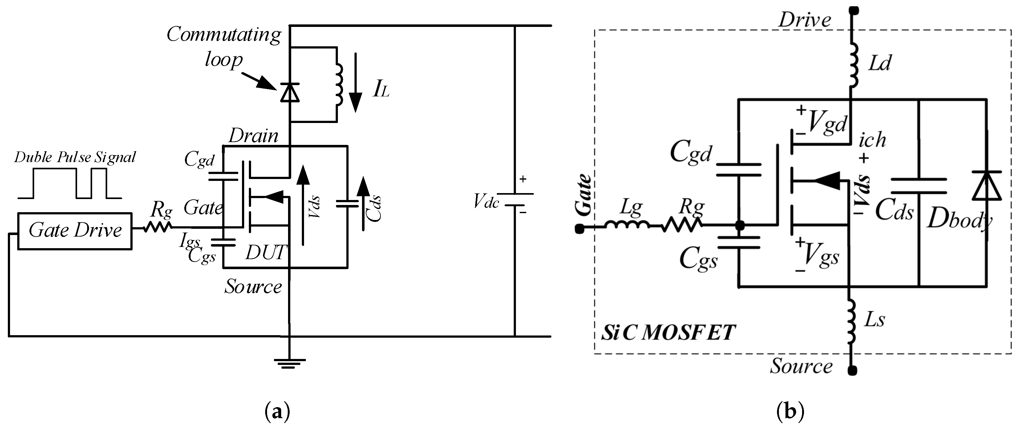
Figure 1a is a typical DPT circuit adopted to assist in modeling the switching characteristics, and the analysis of the switching losses. This switch configuration consists of the switch, with an anti-parallel free-wheeling diode. The lower switch is the Device Under Test (DUT), and the upper part is the SiC SBD. The SBD remains in the off state during the test with its anti-parallel diode utilized as a free-wheeling diode. The circuit equivalent model consists of the main parasitic elements, the varied input voltage source
, and the output drain current
. The reverse recovery behavior of the free-wheeling diode and the parasitic capacitance significantly affects the turn-on of the switch. Whereas,
Figure 1b is dedicated to showing the switch with its parasitic inductance, parasitic capacitance, and the associated voltages of the SiC device. The gate drive signal commutates between −4 V to
(20 V) with insignificantly small rise time and fall time, which is a square wave voltage.
is the gate-source voltage,
is the drain-source voltage and
is the gate-drain voltage. The parasitic elements are the gate-source capacitance
, drain-source capacitance
, and the gate-drain capacitance, also known as miller capacitance
.
is the square wave gate drive output voltage,
represents drain current,
denotes channel current,
the diode current, and
is the cathode–anode voltage of the SiC Schottky Barrier Diode.
is gate drive-equivalent series resistance,
the external gate resistance, and
represents parasitic stray circuit resistance. It is noted in [
20] that the gate resistor
significantly affects the turn-on and the turn-off losses. A low value of
implies a significant reduction of the losses, both turn-on and turn-off. However, a higher
occurs in the switching transients resulting in a significant shoot-through energy density. The common non-linear parasitic capacitance includes the reverse transfer capacitance
input capacitance,
, and output capacitance
. Their values can be expressed in terms of data-sheet parameters as
In this case, the above three capacitance are given in the data-sheet. That is,
,
, and
. Thus, to simulate the dynamic model: the capacitance
,
, and
, are required. These can be obtained from Equations (1)–(3), using the following equations showing their relationship.
=
,
=
−
, and
=
−
. It should be noted that
is almost constant whereas
, and
are voltage
-dependent [
21,
22].
The SiC MOSFET output capacitance consists of gate-source, gate-drain and drain-source capacitance of the switch. The mentioned capacitance have an indirect effect on the switching losses, as they affect the rise time and fall time intervals of the voltage and current.
2.2. Ideal Switching Transcients of SiC MOSFET
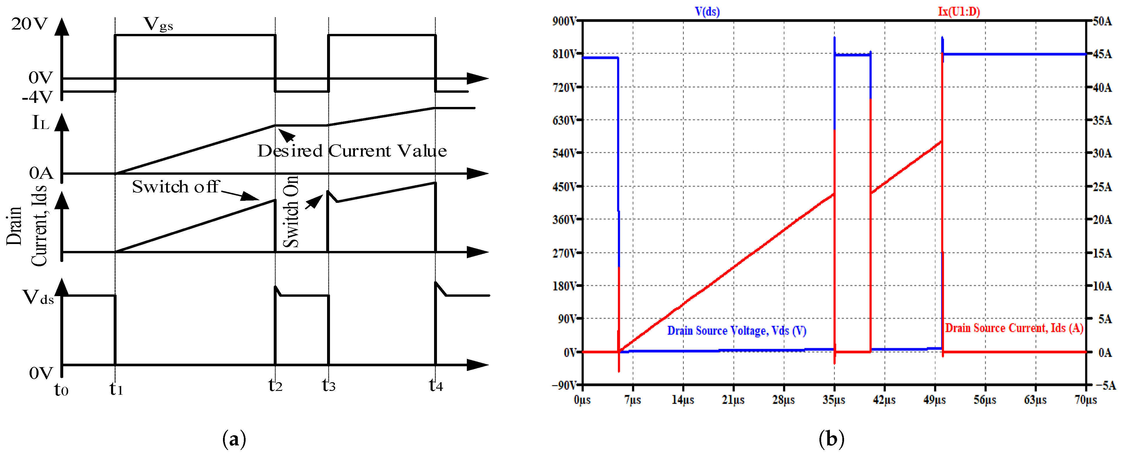
Figure 2a shows the ideal drive voltage and the load current waveform of the DPT, while
Figure 2b shows the actual simulated waveform. In the ideal switching transients, a few assumptions were made in that the inductor does not change during the switching process, the free-wheeling diode is ideal, that is, it does not have a junction capacitance nor forward voltage drop, and lastly that the gate driver is an ideal, step voltage source—that is, the off-stage voltage is zero and on-state voltage lever is
. The authors of [
17,
23,
24] elucidated on the various switching behaviors of Si MOSFET with a flat Miller region and SiC MOSFET whose Miller plateau is non-flat, as it varies with change in
. However, the existing methods assume a constant value of
.
Additionally, during the analysis, a few assumptions are made as follows: and SiC MOSFET is active, with and . When the SiC MOSFET is off, , and . The switch is fully on when .
The switching characteristics of the SiC MOSFET involve the turn-on and turn-off of the switch with charging and discharging of the various non-linear parasitic capacitance. Switching loss constitutes the highest power loss of the power dissipated during the whole switching event [
25]; it is very imperative to note this when computing the converter power losses.
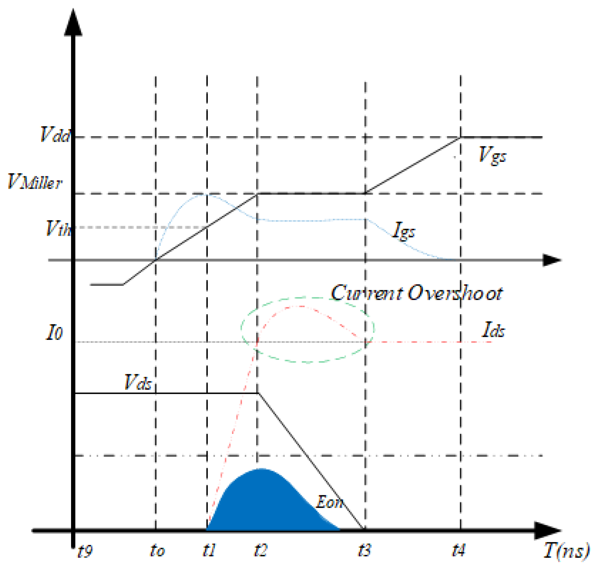
During the turn-on process, as shown in
Figure 3, the switch leakage current rises from its negligible amount to the turn-on current while the voltage which was at maximum, falls to the on-state voltage
, which is significantly small. Ideally, the reverse recovery effects are usually not considered; it is assumed to have a zero voltage drop and insignificant junction capacitance. This is because the SiC technology inherently minimizes their effects since the reverse recovery charge
is insignificant. Additionally, the SiC MOSFET reverse conduction is through its channel rather than the body diode. The turn-on and turn-off are completely independent.
Figure 3 is a typical turn-on event in a SiC MOSFET.
2.3. Turn-On Switching Transients Analysis
It is noted clearly that during the turn-on process, the gate drive circuit state commutates from
to the maximum,
. This initiates the gate-source voltage,
, to increase linearly. Consequently, the drain current linearly increases till the final value while the drain-source voltage drops to the turn-on voltage value
, which is almost zero. This is realized since the free-wheeling diode is forward-biased at the beginning, which forces it to sustain a constant drain-source voltage till the SiC MOSFET conducts all the output current. The working regions of the model are divided into small segments for easy elucidation [
16,
26]. The wave patterns are observed as the gate drive voltage is applied at the gate and source terminals of the switch at normal operating conditions. A brief elucidation of these stages is given in the sub-sections below, noting that increasing the internal drain to source voltage higher than the
) makes the MOSFET enter into saturation.
- Stage 1
(): Turn-on Time Delay ()
Initially, the applied drive voltage between the gate and source is zero or less for SiC technology (−4 V). Then,
begins to rise, and
and
will be charged by the gate’s current
. The majority of the current charges the
, thus is higher than
. As the gate signal is increased, the switch remains in the cut-off region until
reaches the threshold voltage,
. Before the value of
reaches higher than
, the current
remains at zero, which effectively blocks the
[
27]. Gate voltage rises exponentially with a time constant
which is defined by switch-equivalent capacitance
and gate equivalent series resistance
as shown in Equation (
4). The stage has no switching losses generated since the switch is not activated, as it is still off. Generally, the capacitance in this cut-off region is calculated and added to the SiC MOSFET data-sheet parameters [
28]. Only the load current circulates through the SiC Schottky Barrier Diode. This stage ends when
equals
. When the threshold voltage
is higher than the gate-to-source
, the SiC MOSFET remains off, and the value of the drain current
remains zero.
and
do not change [
16,
29,
30]. The initial conditions are
and
;
<
,
:
where
is the charging time constant of the input parasitic capacitance.
is the gate resistance component, which is varied during tests and is connected to the SiC MOSFET gate for the purpose of protecting it against over-current during the turn-on [
31].
remains zero until
equals
. From
Figure 3, the Equations (
5) and (
6) governing this conduction delay region
are
and since SiC MOSFET is open, the capacitor
is being charged thus,
The value of
is fixed and
. From Equations (
5)–(
7), we receive Equation (
8).
Solving the Equation (
9) above provides (
10):
Rewriting and solving for the delay over a period
, equivalent to
, produces Equation (
11):
- Stage 2
(): Drain-Source Current Rise Period ()
Increasing the
, higher than the threshold voltage
, will initiate the switch to start turning on. Drain current
starts to increase linearly from zero to its maximum value
, taking over the load current. This is known as the current rise period. This current increases high above the inductive load current,
. The load current commutates from the free-wheeling diode to the switch, which is still conducting. This is contributed by the free-wheeling diode reverse current.
remains almost constant in this region at blocking conditions [
23,
25]. Its derivative remains zero. The linear transfer characteristic of the switch is given by Equation (
12) [
32,
33,
34]:
where
is the non-linear transconductance of the SiC MOSFET, and with
being as Equation (
13):
From Equations (
4) and (
8), we obtain the value of
as elucidated by Equations (
14)–(
16):
- Stage 3
(): Voltage Fall Time I, Miller Plateau:
In this stage, the free-wheeling diode has been switched off, blocking voltage. The reverse recovery current decreases from
to
, and thereafter remains constant. The Miller effect takes place, and the
is clamped at
. When
is held constant by the external circuit, the SiC MOSFET operates in a saturation or active region known as the Miller plateau, and
thus remains almost constant.
drops fairly quickly from the maximum to the minimum value given by
in this region. The
slope is determined by the gate current that flows through the
.
and
insignificantly varies. Additionally, the SiC MOSFET output capacitance
starts to discharge. In the case of the SiC Schottky diode, it suffers from almost zero reverse recovery effects; only a small portion of reverse current is introduced by its junction capacitance. This reverse capacitance current increases switching losses. At this moment, the total gate current passes through the gate-drain capacitor. Thus, the gate current can be said to be (
16):
The losses in this region can be computed through overlap area between the current increasing and the voltage decreasing.
- Stage 4
(): Drain-Source Voltage Fall Time: Gate Voltage Rise Remaining Charging Time :
In this region, the value of
>
and
> (
). The SiC MOSFET enters into a linear or ohmic region. The drain-source
value falls and reaches its minimum on-state voltage
, and the Miller plateau ends.
charges
and continues to rise till it reaches the maximum of
, which is imposed by the driver voltage, which rises to the maximum value
.
and
are in their steady-state condition. At this stage, the value of
falls to zero as shown in
Figure 3. After this, the switch will be in a conduction state till the next turn-off begins. The current reaches saturation, and the gate-source voltage reaches its operating point, and thereafter becomes constant. The average gate drive current
in this region is given by Equation (
18), whereas Equation (
19) provides the voltage fall time,
.
- Stage 5
(): On-State Operation:
The switch enters conduction mode, during which it conducts the entire inductive load current,
=
. The
at this stage is not zero and contributes to the conduction losses.
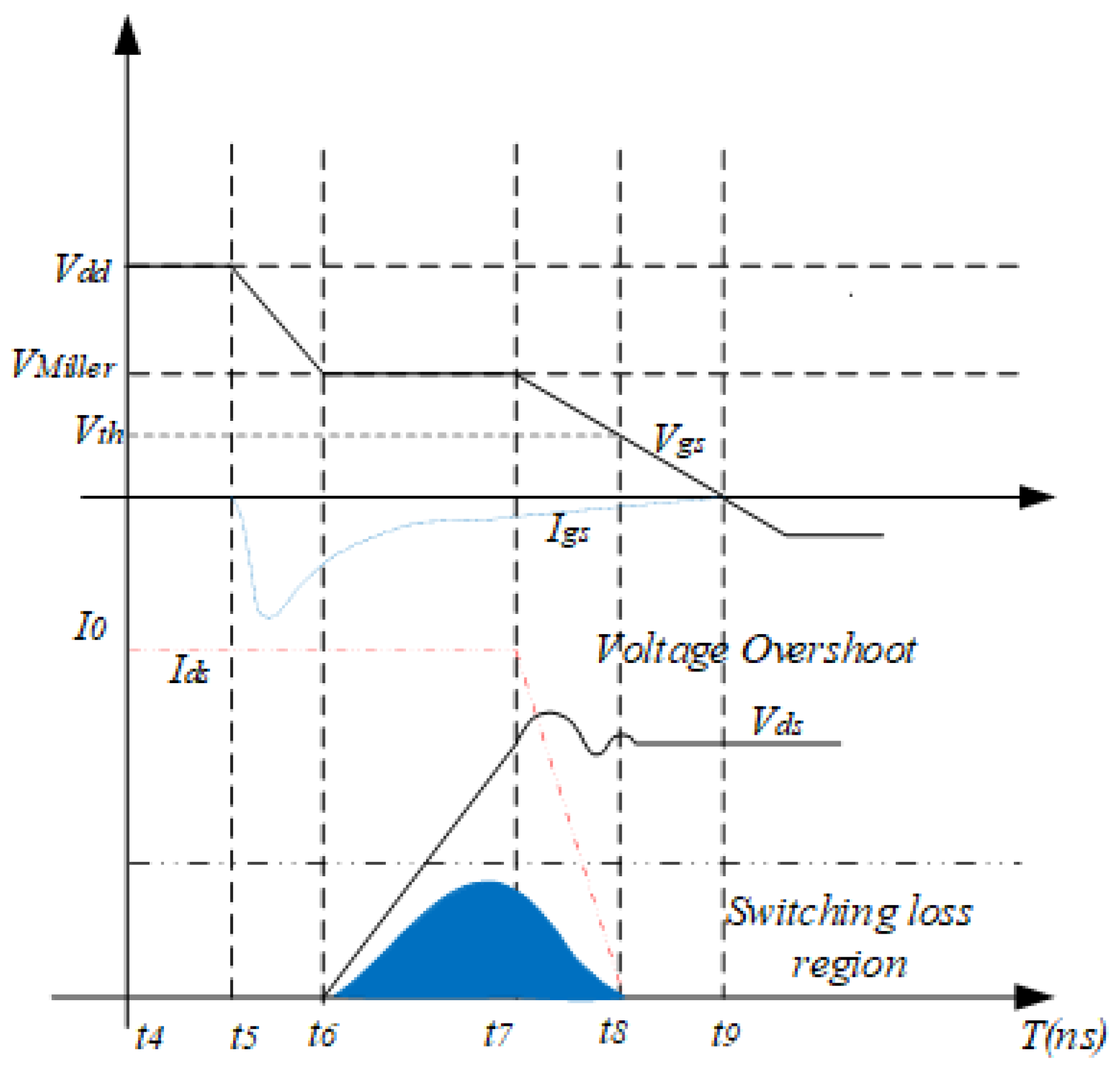
Figure 4 is an illustration of the SiC MOSFET waveform during the off-transition. This includes the gate drive voltage
, the gate-source voltage
, the drain-source voltage
, and the gate’s current
. Since the switch was in an ON state, the value of
is low at the beginning, and
is high. The switch input capacitance
is discharged through
and the
as
begins to decrease when the gate drive
is decreased, as explained in the next stage. Significant SiC MOSFET losses occur in this stage.
2.4. Turn-Off Switching Transients/Transition Process
Figure 4 shows an ideal waveform presentation of the turn-off events of a SiC MOSFET switch. The SiC MOSFET is on and conducting the full load inductive current. The drain-source voltage
is
. The Schottky diode is off. The gate drive voltage imposes a varying voltage
and reduces to a minimum. The gate current
, the drain current
, the gate-source voltage
, and the gate drive voltage
are indicated. During the turn-off transition, the total turn-off energy loss is obtained from the integral of the gate voltage rise and current fall overlap region, present in the
Figure 4 in blue, capturing the transient power dissipation. The turn-off process can be divided into smaller parts for explanation.
- Stage 6
(): Turn-off Time Delay
The gate voltage decreases up to . The voltage remains significantly low, and the switch current insignificantly changes. The rate of decrease is given by a time constant dependent on the switch input capacitance and the gate resistor . The input capacitance is discharged through the gate drive circuit. The turn-off initial conditions are and .
- Stage 7
(): Voltage Rise Time I: Miller Plateau
In this region, the switch is in saturation. The voltage reaches the and remains insignificantly changing within the region. The SiC MOSFET operates in the ohmic region. At the same time, is discharged. and remains constant in this stage. Drain-source voltage rises to the bus voltage .
- Stage 8
(): Drainage-Source Voltage Rise Time II: Current Fall time
The load current
starts to divert from the switch to the free-wheeling diode as the free-wheeling diode is no longer blocking voltage, as it is forward-biased.
quickly decreases to zero at the end of this region. An overshoot of
occurs in this region due to the parasitic component induced by the current. This stage ends when the
drops to
. Once the drain current decreases, the SiC MOSFET suffers extra voltage stress, as there is a voltage drop across the parasitic inductance. The drain-source voltage rise time is given by Equation (
21) as
- Stage 9
(): Current Falling Time/Voltage Ringing Time :
The drain-source voltage
forms oscillations (ringing) since parasitic components exist (stray inductance and SiC MOSFET output capacitance) and thereafter remains fairly constant after the overshoot at
. The stray capacitance eventually damps the high frequency, and all the remaining energy is dissipated, whereas the value of
continues to exponentially decrease with a constant dependent on
and
till it reaches zero. The value of
is given by Equation (
23) as
- Stage 10
(): Off-State Operation:
When the reaches the maximum threshold , the drive voltage is reduced to zero, and thus the gate-source voltage becomes zero. The SiC MOSFET turns completely off in this region.
2.5. Analysis of Switching Losses in SiC MOSFETs
- i.
Conduction Loss.
When the SiC MOSFET is in operation, there are various power dissipation losses which include the conduction loss, the switching loss, the current leakage loss, and reverse-recovery losses of the body diode. The leakage current loss in SiC MOSFET is usually far less than the conduction power loss; this, therefore, is neglected in the preceding study. In some instances, at very high frequencies, this may not be neglected.
Additionally, there is an insignificantly small to almost zero reverse recovery charge due to the use of the Schottky diodes, which are the majority of device carriers in SiC devices; this means that there is no reverse recovery charge. The implication is that for the computation in this manuscript, the recovery loss of the diode is also ignored [
35,
36].
On the other hand, the conduction power loss occurs when the switch is in the on-state, that is, the voltage, which is a function of the current flowing through the switch. The drain-source current
rises during the conduction and causes heating primarily due to the on-state resistance
that passes through. The conduction loss is temperature-dependent as it depends on
, which is a high-temperature-dependent parameter. Since
is not a constant parameter, it varies in response to changes in
, drain-source current
, and temperature. The value of
has a distinct positive temperature coefficient characteristic; thus, its value is usually higher at higher temperatures [
37].
The instantaneous conduction loss via the SiC MOSFET and diode can be obtained as follows [
38]:
With
and
as the instantaneous SiC MOSFET and SBD conduction loss, and
and
as the duty cycle for the SiC and SBD, respectively. The average conduction loss during a fundamental cycle can be calculated using Equations (
26) and (
27) as follows, where
to
is the conduction period of the switch as shown in
Figure 3 and
Figure 4.
- ii.
Switching Loss.
The switching power loss of the SBD, in this case, is usually very small. This is because the switching energy of the SBD is very insignificant in comparison with the SiC MOSFET switching loss [
39]; thus, in this discussion, this is neglected. The increased size of SiC MOSFET leads to a corresponding increase in its intrinsic parasitic capacitance, not limited to the gate-to-source
, gate-to-drain
, and drain-to-source
capacitances. This results in higher charge storage and discharge requirements during the switching transition, which thereby increases the overall switching losses. Ideally, the switching power loss occurs as a result of the overlap of the non-zero current and voltage in the drain-source path during switching, that is, during the switching turn-on events and turn-off events, thereby dissipating energy. This causes power loss as a result of the changing and discharging of the gate-source and gate drive parasitic capacitances (hence called switching power loss). The switching turn-on and switching turn-off energy dissipated is depicted as in Equations (
28) and (
29):
where
and
are the current flowing through the switch during the switching-on and -off transitions,
and
are the total energy loss during the switch on time and switch off time, and
is the switching frequency. The switching-on transition period is shown in
Figure 3, where, at this stage, the voltage
increases and the current
decreases as the transition occurs. This is the period in which the turn-on losses occur due to the overlap between the rising current and decreasing voltage. Therefore, the
period ranges from
to
, i.e.,
Similarly,
Figure 4 shows the
switching period spanning from
to
, corresponding to
and
transitions. That is,
. Equation (
15) provides the current rise time
whereas Equation (
19) provides the voltage fall time
. The summation of these two equations produces the total turn-on time, shown by Equation (
30):
The turn-off period is given by the summation of the voltage rise time
and current fall time
, which are given by Equation (
21) and Equation (
23), respectively, giving Equation (
31):
Therefore, the turn-on switching power loss and turn-off switching power loss are given by Equations (
32) and (
33) as
This implies that the total switching power loss is given by the summation of Equations (
32) and (
33), giving Equation (
34) as
The summation of the above losses associated with the switching device was used to quantify the efficiency. It is clearly noted from Equations (
30) and (
31) that the time taken during the transition plays a significant role in the amount of losses dissipated, with a prolonged switching period depicting more losses and vice versa.
3. Electrical Circuit Analysis
3.1. Model Parameters Description, DPT Model Circuit Analysis
A typical dynamic circuit characteristic of the power SiC MOSFET was characterized in the half-bridge inductive DPT circuit. At the end of the first pulse, the switch was tested for the turn-off characteristics. This was because the inductor current rose to the desired value, after which the inductor current flows through the SBD free-wheeling diode freely till the start of the second pulse, when the device was tested for the turn-on losses [
40,
41]. In this case, this was extended to the second pulse, where the turn-on and turn-off simulation results were considered, as this enhanced a stable situation in the switch. To analyze the influence of varied
on
transient response, the drive voltage,
, which is a square wave with an amplitude equal to
and corresponding switching frequency
and duty cycle, D, is supplied at the gate terminal of the DUT.
Table 1 below shows the extracted data-sheet parameters for the SiC MOSFET used in the voltage-current characterization.
The Wolf-speed Schottky Barrier Diode (C4D20120A) parameters are indicated in
Table 2, and were chosen for this work, as its optimal voltage corresponds with that of the DUT. The SiC SBD diode parameters extracted from the manufacturer’s data-sheets were used in the model and simulation work of this manuscript.
Table 3 shows the critical SiC power device parameters and their impact on the output of the DUT. As can be observed in the table,
is a temperature-dependent parameter; it is assumed that the SiC MOSFET junction temperature is equivalent to ambient temperatures of (25 °C) throughout the work. This implies that the
given in the manufacturer’s data-sheet at ambient temperature is used for the simulation and computation since the temperature at the junction is not affected by power loss within a short period. However, in the preceding work, the variation of the value of
was adopted to study its effects. Additionally, the other assumptions made are as listed in [
42].
3.2. Simulation Results
The Double Pulse Test was utilized in evaluating the switching transitions, specifically during the turn-on and turn-off transitions. During the simulations, the gate resistance was varied in steps from to . The load current was varied from A in steps of 4 A up to 36 A. This could have been increased since the maximum the switch can operate with is 60 A. However, the data-sheet maximum DC continuous drain-source current is 36; thus, this was considered in these tests. The DC voltage initially considered was 800 V. However, to receive the effect on variation of the DC voltage, this was also varied from 200 V to the maximum drain-source voltage of the device, which is 1200 V.
It should be noted that the inner equivalent gate resistance of the SiC MOSFET is not zero. The Wolf-speed Device Under Test has an internal gate resistance of at test conditions of . The test driver circuit, which is basically used in practical tests, does have an internal gate resistance; thus, it is another source of gate resistance to the gate of the switch under consideration. Other parameters that are not mentioned were not modelled.
This proposed design was simulated using LTspice, and the plots are listed below.
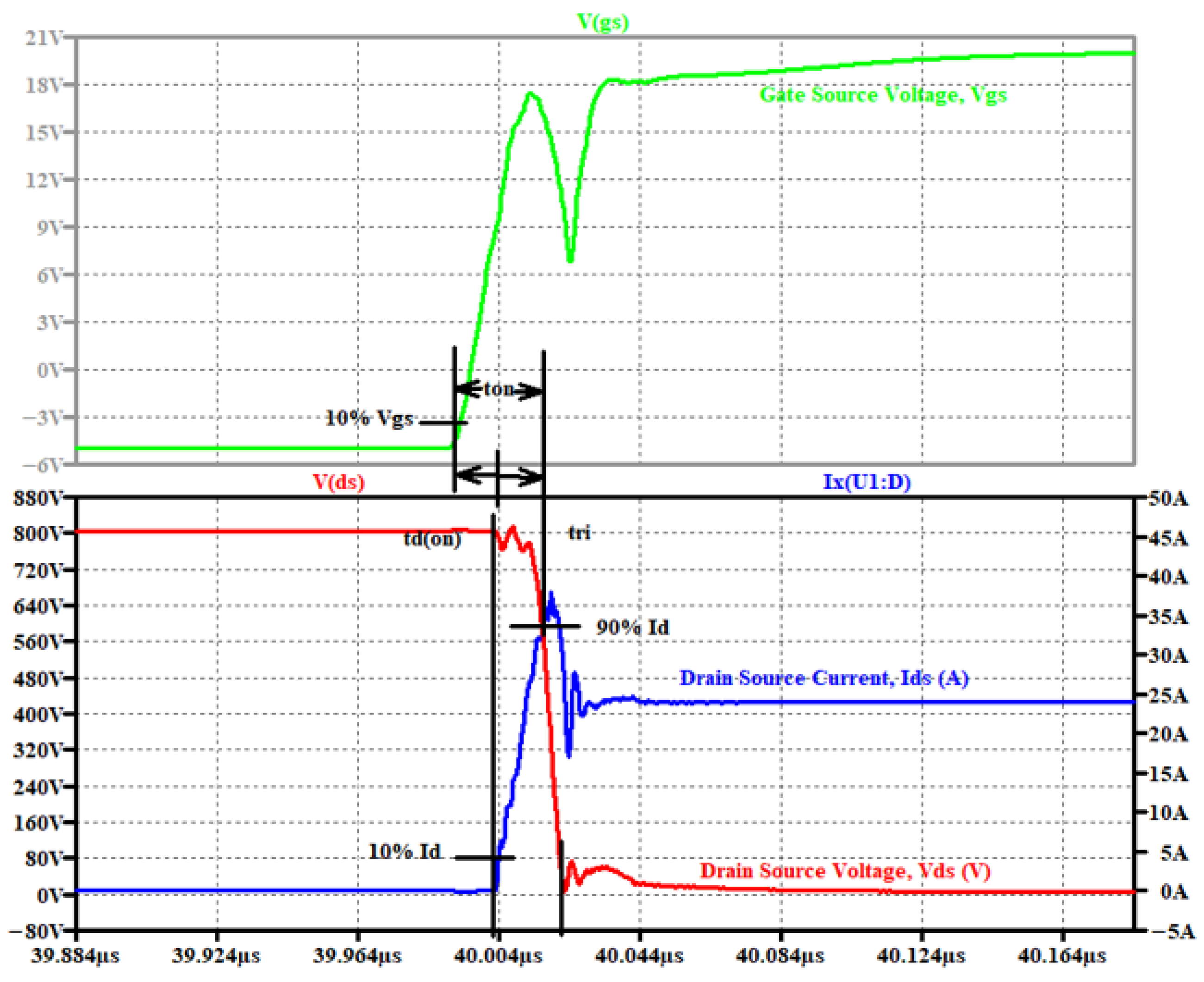
Figure 5 shows the switching waveform of the SiC MOSFET during the turn-on event.
The waveform of the drain-source voltage
, drain-source current
, and the drive voltage
, which is the gate-source voltage, are plotted for specific switching intervals to show the switching transitions.
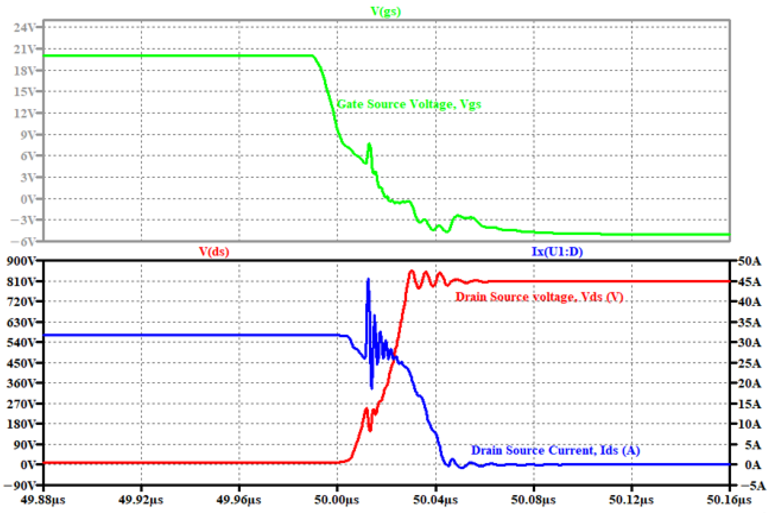
Figure 6 is an illustration of the turn-off transition where the voltage increases from the on voltage
to maximum voltage, and the current
falls from maximum to the minimum value. The upper part of both
Figure 5 and
Figure 6 shows the variation of the gate-source voltage
during the two switching transition periods.
It is known that the value of
has a significant impact on the switching behaviors. This is because it affects the rate of charge and discharge of the gate-source capacitances
and
. Tests were performed at
= 800 V and a constant drain-source current
. The gate resistor
was varied from
to
. For higher values of
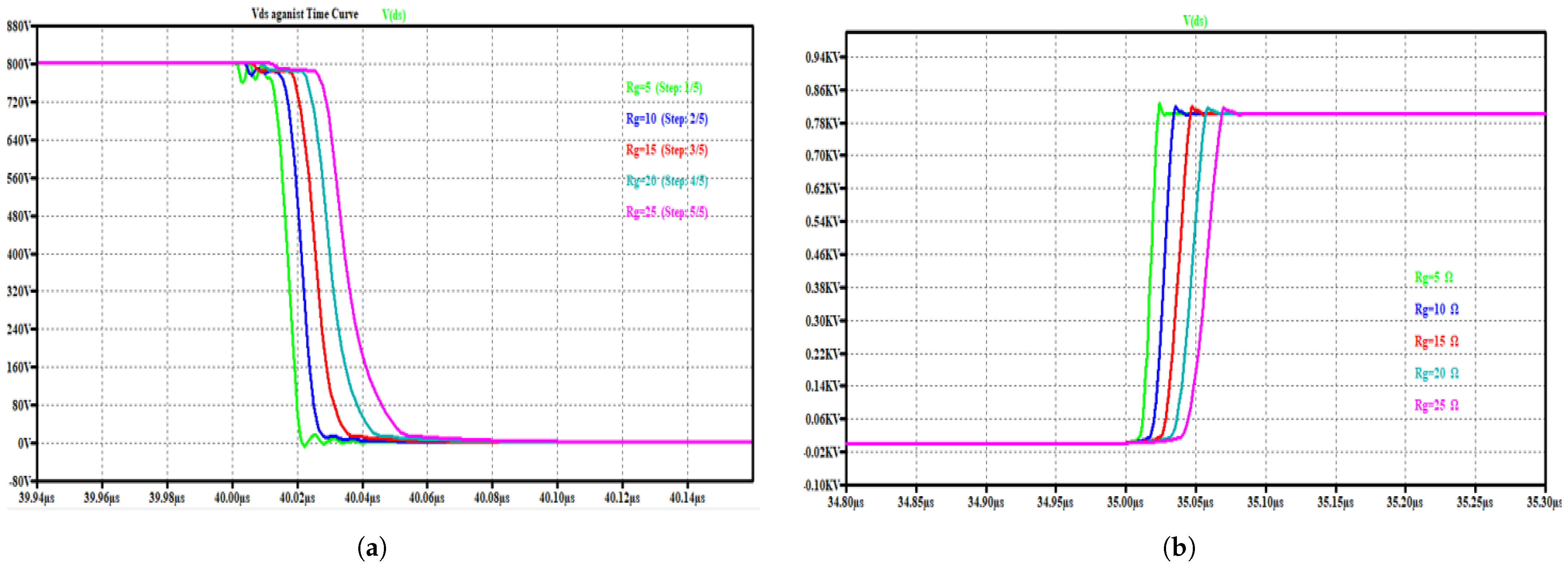
, the transition is slower (takes more time) and the transition during the over-voltage is minimized. This is seen in
Figure 7a,b for turn-on and turn-off, respectively, for current transitions, and
Figure 8a,b, for voltage transitions.
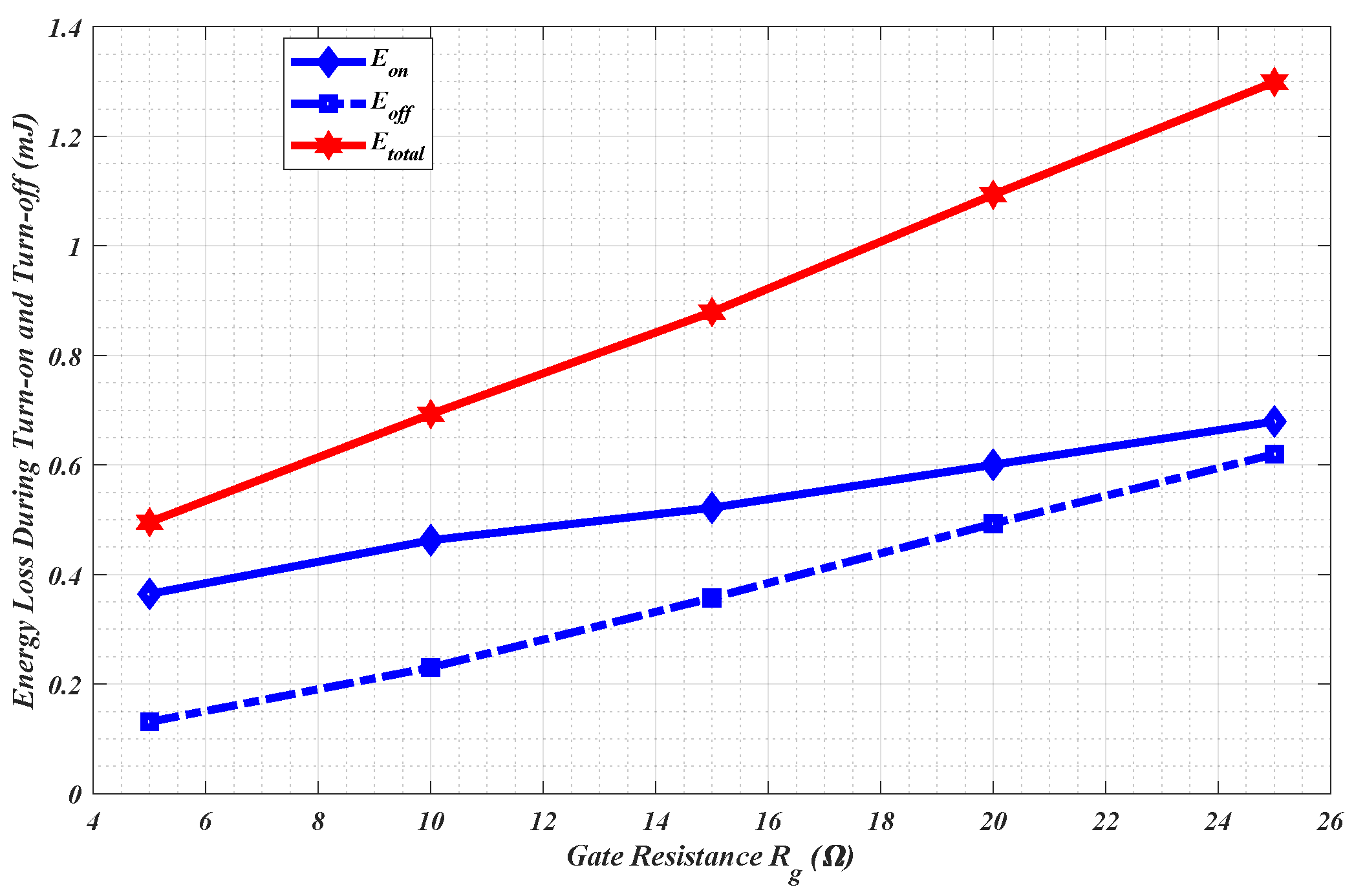
Figure 9 shows the energy loss as the gate resistor is varied. As the gate resistance
is increased, the slope increases. That is the amount of energy lost as the value of
is varied from
to
increases. For
, the turn-on energy is
and turn-off energy is
, respectively, while at
, the turn-on energy is
and turn-off energy is
, respectively. The total energy loss curve indicates a linear dependency on the value of the gate resistance. This behavior is consistent with the simulations and measurements reported in [
43].
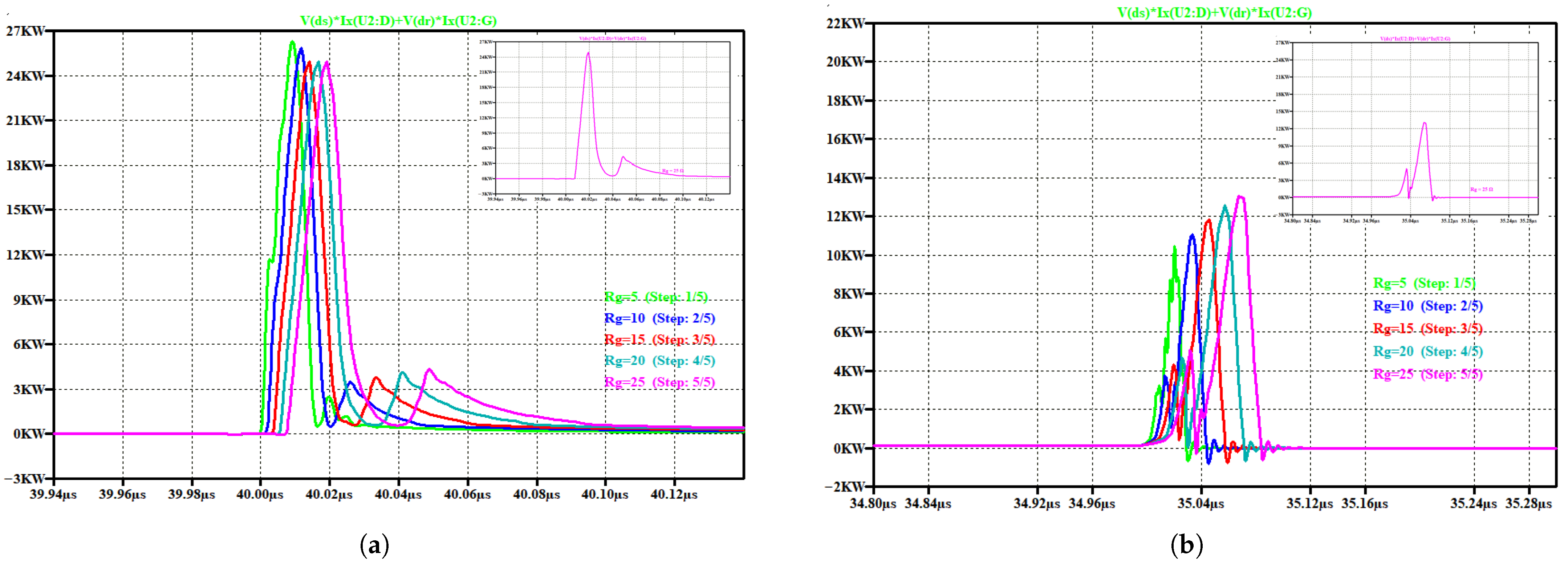
The turn-on loss characteristics are observed from the plots of power loss during the turn-on process.
Figure 10a indicates that the loss strongly depends on the gate resistance (
). As observed, the total energy loss during turn-on increases as the value of
increases, despite the reduction in peak power loss. This is because the peak power loss shifts to the right (indicating a longer and more gradual turn-on time), leading to a broader power dissipation curve. This suggests that higher
results in slower switching, and the transition is slower, so the amplitude of the gate oscillations is reduced, but this increases power dissipation. That is, the wider the power dissipation curve, the longer the turn-on time and, consequently, the higher the energy loss. When
is lower, the turn-on transition occurs more rapidly, leading to reduced turn-on energy loss. However, excessively low
can cause voltage overshoot, high transient current, Electromagnetic Interference (EMI) noise concerns, and increased
, thus the device current spike increase. Moreover, during the turn-off, as the gate resistance decreases, the fall time of the current decreases. If there was a fast turn-off, there would be a subsequent increase in
, and the device overshoot and oscillations would increase.
Since the gate resistance controls the gate charging and discharging speed, it dictates the speed at which the gate turns on or off. Also, higher gate resistance limits gate current, thus more time is taken to reach , increasing power dissipation. Slowed turn-on also means an extended overlap period of and with the resultant increase in the instantaneous power dissipation.
Optimizing the value of is critical in balancing thermal performance, switching loss, and EMI considerations. This implies a trade-off between switching efficiency and EMI control while ensuring overall circuit robustness. Therefore, selecting an optimal value is essential for achieving the best performance of the SiC MOSFET in high-frequency power applications.
As in the case of the turn-on loss plot, the turn-off plot in
Figure 10b exhibits a strong dependency on the value of the gate resistance (
) as well, which influences both the peak power dissipation and the switching energy. The higher values of (
) lead to higher peak power loss attributed to slower turn-off transition time resulting from restricted charge injection rate to the gate. However, this leads to gradual voltage and current overlap over a longer duration, which increases the energy loss. In contrast, the lower values of
enable a fast turn-off process (sharper transition) with lower peak power curves, leading to less energy loss. However, this can potentially cause higher switching noise, thus requirements for an optimal value of (
) to balance the switching loss, EMI, and thermal efficiency. In both
Figure 10a,b, a single curve demonstrating the area under energy loss during the turn on and turn-off loss when
=
, was inserted, respectively.
3.3. Turn-On Switching Transients/Transition Turn-On Switching Transients Simulations Results
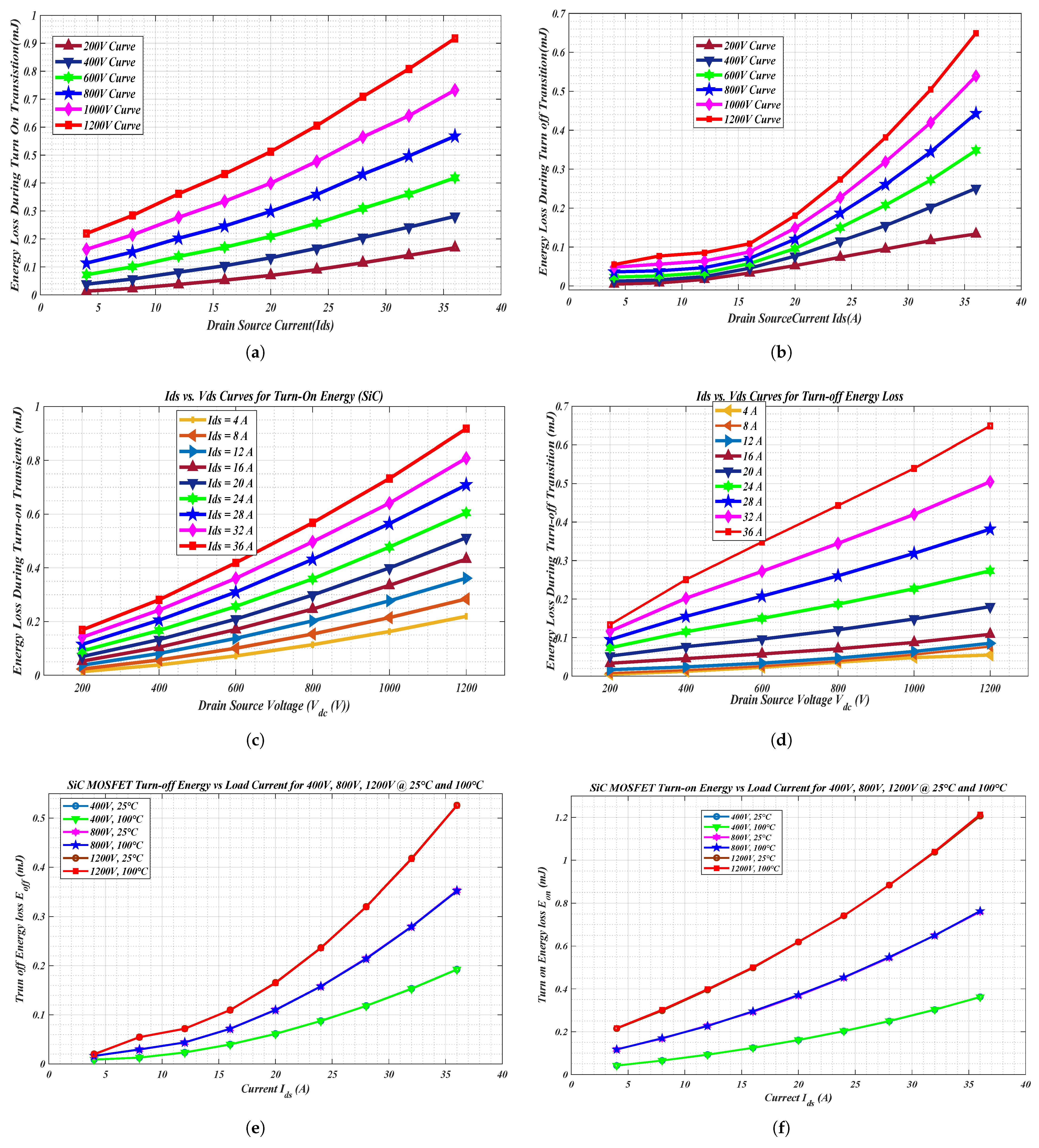
The turn-on energy is contributed by the overlap between the decreasing
and increasing value of
. As the value of
increases, as observed from
Figure 11a, the value of energy loss increases. It is observed that at elevated values of
, that is, from 200 V to 1200 V, there is a proportional increase in the turn-on energy loss. This demonstrates the impact of higher voltage stress on turn-on energy dissipation. On the other hand, a non-linear behavior is observed in the plot of
Figure 11b during low values of
. However, at elevated values of drain current
, the turn-off energy curve shows a significant increase in the losses, and is more pronounced at higher voltages. These variations show that the turn-off losses are influenced by both the current and voltages, with higher values exacerbating power dissipation during switching. It is observed in
Figure 11c,d that the turn-on energy loss increases as
increases, and is strongly dependent on the drain current, with a higher current resulting in subsequent high energy loss during both the turn-on and turn-off transients.
Figure 11e,f show the turn-on and turn-off energy loss evaluated across different DC-bus voltages, currents, and temperatures. The observation was that at elevated voltage operation, the turn-on became dominant switching losses in comparison with the turn-off energy loss. However, there is minimal influence observed from the temperature variation across all conditions. This is due to lower reverse recovery effects. This implies that SiC maintains predictable switching behavior over wide thermal changes, thus showing thermal robustness, which is an advantage of the SiC at high temperature operations. It can be inferred that the high-voltage high-current operation leads to large losses, for both turn-on energy loss and turn-off energy loss, thus the necessity for soft switching during the design of the converter when using the SiC MOSFET devices.
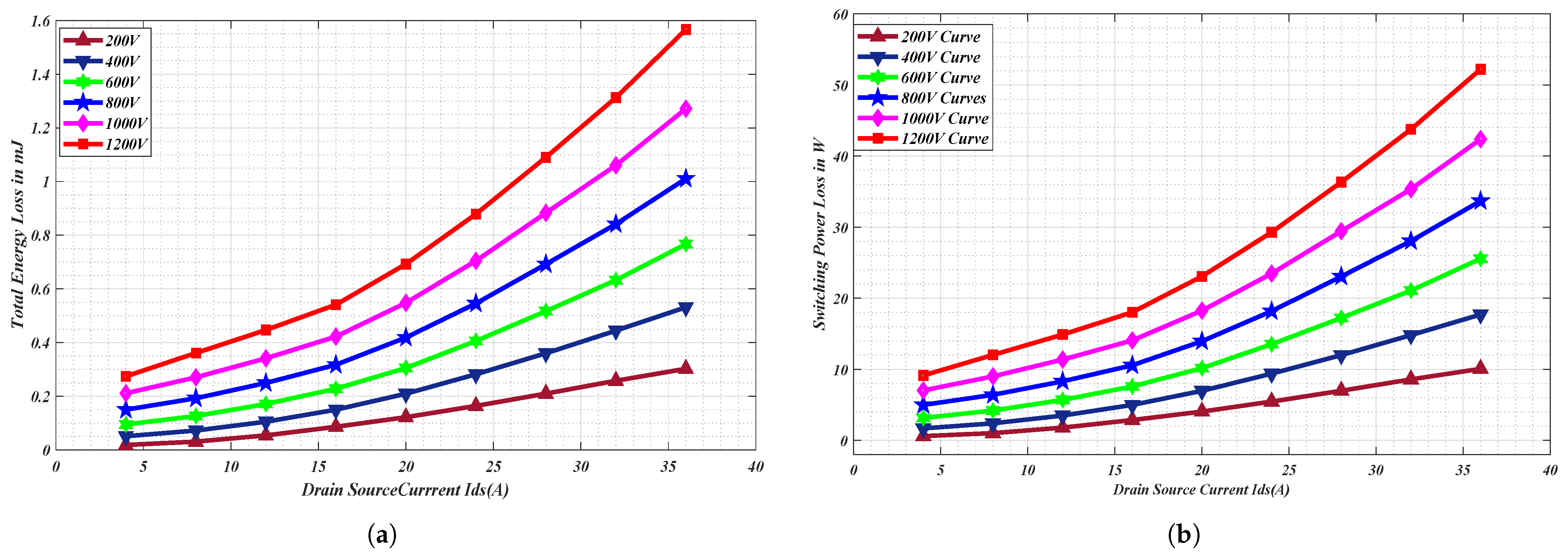
Figure 12a shows an illustration of the summation of the total energy loss during the turn-on and turn-off transition. That is, the total amount of energy loss during a complete switching transition, with various steps of current variations. Considering the input DC voltages at discrete points and currents, which are being varied, the summation of the turn-on energy loss and turn-off energy loss shows an increase in the loss as the current passing through the switch is increased.
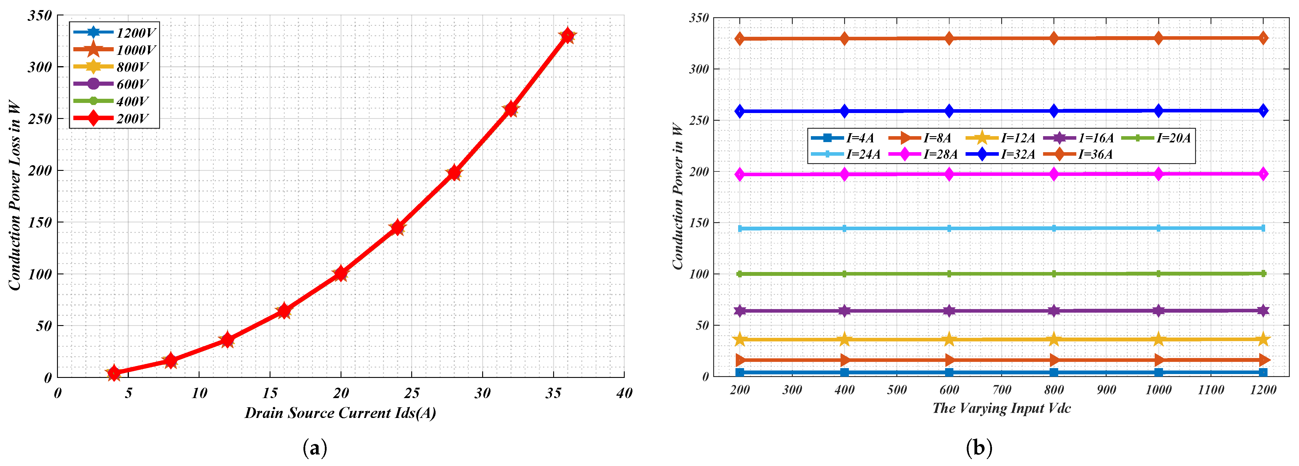
Figure 13a shows conduction power loss with varying
. The figure shows that the conduction power loss follows a quadratic increase with an increase in drain-source current
, and various voltage curves overlap. Let us say, at 20 A, the conduction power loss for the 200 V to 1200 V curve remains consistently at approximately 100 W, and at 36 A, the conduction power loss is approximately 329 W with a small variation with changes in
. This implies that the conduction loss does not change with changing
, as can be seen from
Figure 13b, where the conduction loss remains significantly the same, thus a flat curve. The reason for this is that conduction losses are highly dependent on
and the device’s on-resistance
than applied DC voltage.
This acts as a confirmation that the SiC MOSFET is predominantly dependent on the drain current and the device’s on-state resistance, rather than on the applied voltage. Each curve on the
Figure 13b corresponds to a specific drain current
(4 A to 36 A), with higher currents resulting in significantly high losses. This invariance of the conduction losses with respect to
acts as a confirmation that in the event of switching, the conduction power loss dissipated is independent of the switching events. In conclusion, higher current leads to significant conduction losses. In
Figure 13b, the conduction power loss characteristic is clearly seen across different varying voltages. Since each curve corresponds to a specific
, higher current results in higher losses.
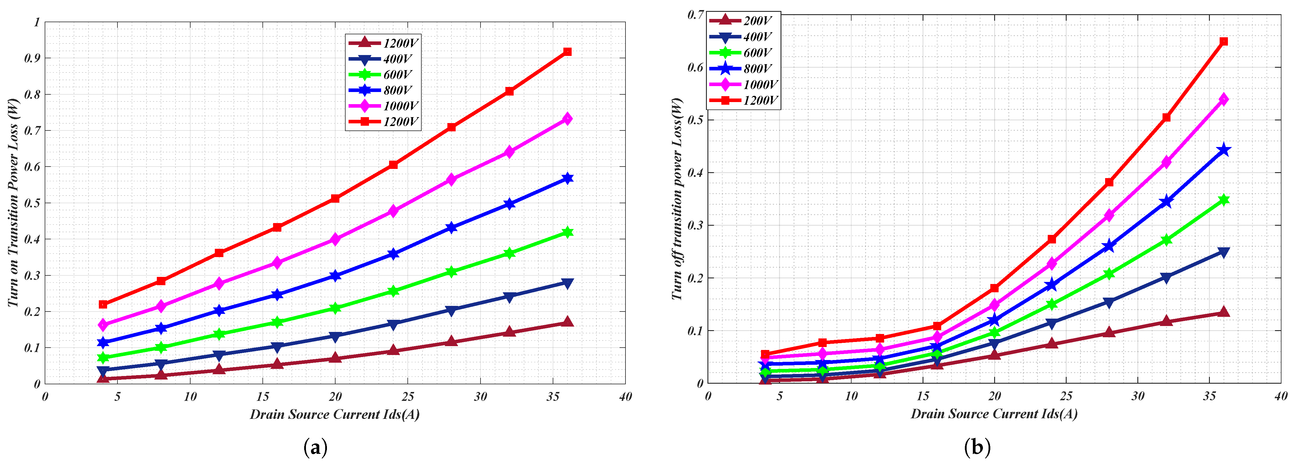
Figure 14a is a graph that represents the turn-on power loss transitions. As the value of
and
increases, there is a consistent increase in the power loss. Higher voltages (1200 V) exhibit a greater voltage loss than the lower voltages (200 V). The turn-off transition power loss shown in
Figure 13b shows a similar pattern, though with a steeper rise in losses for higher current values. It is clear that at low values of current,
= 20 A, the loss is relatively small, beyond which the power loss becomes significantly pronounced. The variation in the two curves is an indication that the power turn-on and turn-off power loss is strongly influenced by both the current and the voltage.
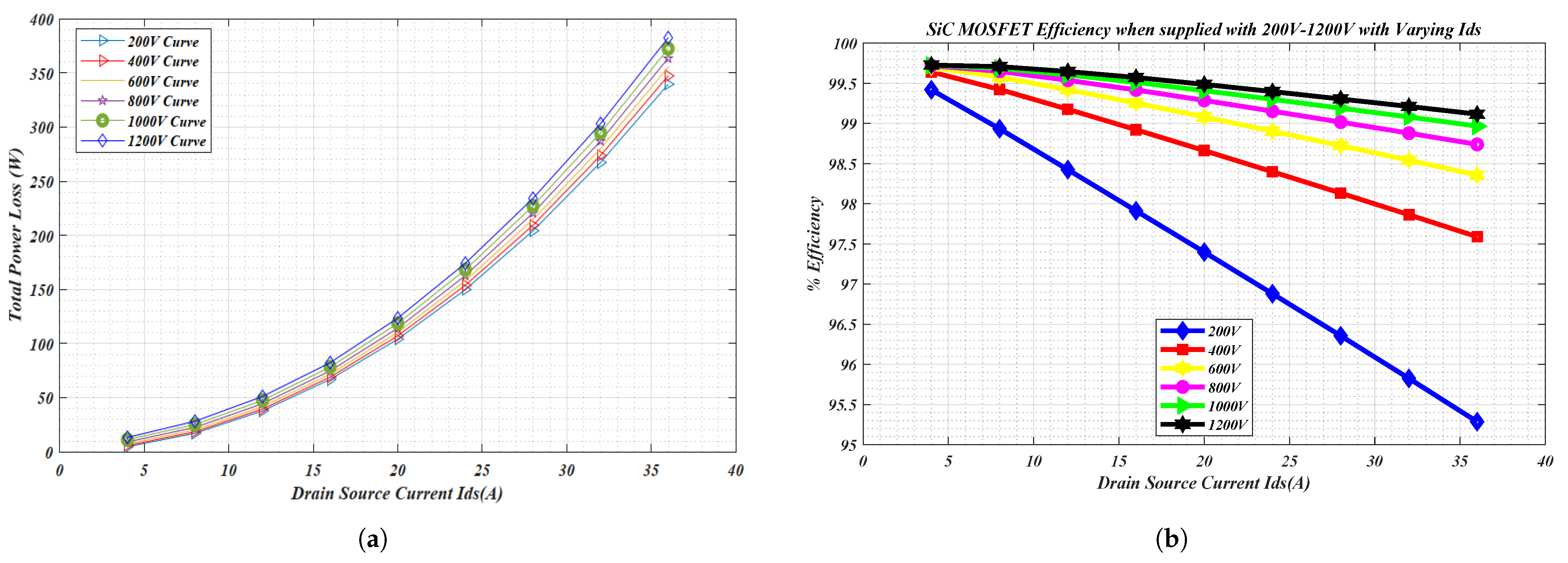
Figure 15a shows that the cumulative power loss in a SiC MOSFET is significantly high at high voltages, and lower at low-voltage levels. However, there is a smaller variation in the total loss due to voltage variations at a specific drain-source current. As the current increases, the losses increase to higher values.
It should be noted that, at the same power output, the efficiency is significantly higher at high voltage as compared to operation at lower voltages. This is because at higher voltages, the conduction loss remains significantly the same as the loss at lower voltages. SiC MOSFET also exhibits properties of lower at higher voltages. Whilst switching loss increases with switching voltages, they do so at a lower rate in comparison to the conduction loss. Since high-voltage switches are well optimized for faster switching and high voltages, they have lower transitional losses at high voltages. However, extremely high voltage can result in the turn-on and turn-off losses being higher as a result of high energy dissipation during the transition.
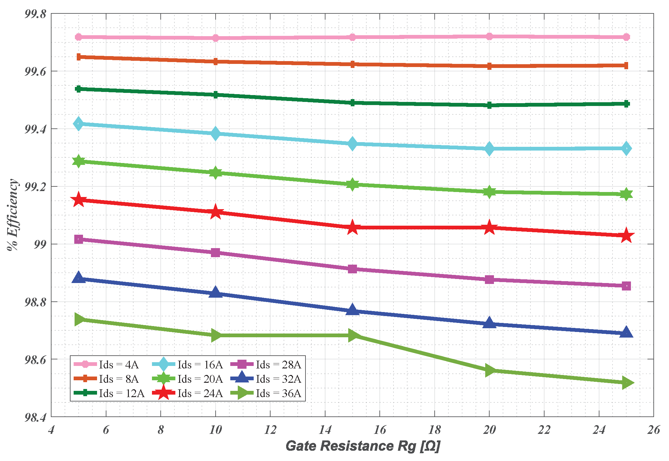
In contrast, at lower
, even with variation of gate resistance, the efficiency remains significantly high. This is seen in
Figure 16, as when
= 4A, the efficiency is noted to be 99.71% at
and 99.71% at
, showing an insignificant deviation of 0.00005%. At higher
, the efficiency is observed to be a bit lower at 98.73% for
as compared to 98.51% at
.
3.4. Application and Discussion
In this section, the potential of the SiC MOSFETs integrated with Schottky Barrier Diode in a power converter is critical, as this leads to improved performance and significant power dissipation reduction. The combination, which has significant fast switching and high frequency, leads to low switching loss, lower power dissipation, and thus high efficiency. The modules designed for the devices are well suited, particularly for the high-power, high-density, and high-frequency applications, which among them include and are not limited to hybrid electrical vehicle traction inverters, electric vehicles, high-voltage DC transmission systems, solid-state transformers, renewable energy integration systems, PV DC-DC converters, and industrial motor drives among others [
44]. Attaining high power density, high efficiency, and reliability are critical in these devices.
The process of characterization of the SiC MOSFETs plays a critical role during the design of high-efficiency converter. The multi-parametric variation emulates the actual working environment where different parameters are varied simultaneously. The quantification of power dissipation depends on gate resistance, current, and voltage under realistic operating condition, which is critical in ensuring the right gate resistance is chosen, switching frequency is optimally selected, and cooling strategy implemented. Moreover, the converter designer gains prerequisite insights on predicting the EMI noise and their mitigation techniques, ensuring the ZVS/ZCS operation is achieved to lower the voltage and current overlap during the turn-on and turn-off switching transitions events, significantly reducing the switching time; thus an informed choice of switching frequencies, the size of magnetic, heat-sink, and design of adaptive and active gate drivers can be optimally achieved.
The theoretical analysis is validated, which is critical when proposing methodologies for optimization and improving the converter performance, as there is knowledge of how the device performs when subjected to different varying input–output parameters. Thus, it is possible to design a more reliable system that is less sensitive to input variations during the operations. Additionally, the knowledge of influence due to these parameters in the inductive clamp circuit would otherwise help in peak voltage stress mitigation, and current slew rate mitigation during the switching, ultimately improving reliability of the device, reducing aging, and improving the converter lifespan.
Investigating these parameters’ influence on high switching frequencies and high switching speeds is imperative in that it is possible to alleviate the EMI noise associated, which could result in damaging the converters, the device supplied by the converter, and other accessories that would otherwise be expensive to replace. According to the authors of [
45], it is demonstrated that the SiC device offers significant advantages; thus, in any application, a clear understanding of the device is prudent to ensure high reliability.
When the converter operates in hard-switching, the inferred information helps in balancing efficiency against EMI noise, as well as voltage oscillations and overshoots by correct selection of that maintains and within limits while minimizing switching and gate drive energy loss. The optimal selection of the value of should ensure that the acceptable voltage overshoot, EMI noise, , , peak driver current, and switching losses are within the system limits. These can be easily picked from the DPT results obtained for the minimal loss. These parameters must be evaluated together, as variation in the value of has a direct influence to all the others simultaneously. The implication is that the Double Pulse Test is a simple arrangement that is easy to perform, providing the data set for the designers. DPT produces the values for the on–off energy loss, overshoot, current, and voltage slew rates for each step value of , making it easy for the designers to perform the appropriate tests before designing a full converter, ensuring that they fully quantify the power losses.
3.5. Limitations
This study presented a detailed evaluation of the impact of variations of different parameters on the losses and efficiency. These results are valuable since they are obtained using manufacturer-provided device models and have been validated to provide reliable insight into the switching behavior of the device across different operating conditions, as they closely present the actual device behavior. The multi-parametric approach adopted provides insights into device behavior that could otherwise be difficult to experimentally obtain. Thus, the simulation study provides a credible foundation for understanding and guiding practical design. Nevertheless, it may need future experimental verification.
