Article

A Si and SiC Hybrid Arms ANPC Converter Achieving Comprehensive Optimization of Power Quality, Efficiency, and Cost

1
College of Electrical Engineering, Zhejiang University, Hangzhou 310027, China
2
Zhejiang University-University of Illinois at Urbana-Champaign Institute, Zhejiang University, Haining 314400, China
*
Author to whom correspondence should be addressed.
Energies 2025, 18(23), 6198; https://doi.org/10.3390/en18236198
Submission received: 19 October 2025 / Revised: 16 November 2025 / Accepted: 25 November 2025 / Published: 26 November 2025
(This article belongs to the Special Issue Control and Optimization of Power Converters)

Abstract

Wide bandgap (WBG) power semiconductors such as silicon carbide (SiC) can significantly improve the performance of multilevel converters. However, there are three challenges for large-scale application: high cost, limited power ratings, and reliability issues. In this paper, we propose a Si and SiC hybrid arms active neutral-point-clamped (ANPC) converter, using smaller current rating SiC devices compared to other Si devices in this topology. By employing the hybrid-frequency modulation scheme, the Si devices switch at fundamental frequency (FF) or low frequency (LF), while the SiC devices switch at high frequency (HF). The equivalent circuit of the proposed converter is derived to analyze the principle of LF current ripple compensation. The closed-loop cooperative current control strategy is proposed to realize unequal current sharing in two arms and complete LF current ripple compensation. The Si arm processes major power, while the SiC arm compensates the LF current ripple generated by the Si arm and processes minor power. The proposed topology and control strategy are validated by simulation and experimental results. Compared with the existing typical topologies, the comprehensive optimization of power quality, efficiency, and cost is realized.

1. Introduction

Multilevel converters have evolved over many years and are considered a preferred solution for electric energy conversion in high-power applications [1]. Recently, with the rapid development of emerging power conversion applications such as renewable energy generation [2], electric vehicles [3], more electric aircraft (MEA) [4], and medium-voltage motor drives [5], the efficiency, power quality, cost, and power density of multilevel converters have reached a higher level. Due to the inherent material limitations of silicon, the operating temperature and switching frequency of Si-based devices are approaching their theoretical boundaries. As a result, enhancing the performance of high-power multilevel converters based on silicon devices has grown increasingly impossible. WBG power semiconductors represented by SiC MOSFET feature high voltage withstanding capability, low on-state resistance, and high switching frequency [6], which can further improve the performance of multilevel converters. However, the large-scale application of SiC devices still faces three major bottlenecks: high cost, limited power ratings, and reliability issues. Firstly, a SiC MOSFET is four to eight times more expensive than a Si IGBT, particularly in the high current ratings [7]. Secondly, the maximum current rating of an individual SiC MOSFET die lags significantly behind that of a Si IGBT. Thirdly, compared with Si IGBTs, the ruggedness and reliability of SiC MOSFETs are still subjects of widespread concern, particularly due to unresolved issues such as gate oxide degradation [8], threshold voltage drift [9], and body diode reliability [10]. Therefore, the large-scale industrial application of SiC devices in high-power multilevel converters remains significantly constrained.
To overcome these challenges, researchers have introduced hybrid concepts that combine the strengths of both Si and SiC devices. One widely adopted example is the hybrid three-level (3L) ANPC converter, which offers a practical balance between efficiency and device cost in advanced grid-connected inverter and rectifier systems [11,12]. In high-power rectifier applications, hybrid unidirectional rectifiers using SiC MOSFETs and Si diodes in 3L and five-level (5L) topologies have been proposed to reduce system cost in [7,13]. Similarly, three five-level converters with hybrid Si and SiC legs were presented in [14,15,16]. The above designs employ hybrid-frequency modulation strategies where Si devices switch at fundamental or low frequency, and SiC devices operate at carrier frequency. Thus, these topologies have lower losses, improved harmonic performance, and reduced cost. However, the SiC devices in these topologies handle the full load power, which results in relatively high cost. Moreover, the topologies in [14,15,16] are just single-phase circuits, which cannot be applied to three-phase high-power scenarios. Therefore, how to configure a three-phase hybrid multilevel converter with lower cost and better performance is still a challenge.
Recently, a novel concept known as WBG fractional power processing (WFPP) has been introduced [17,18,19]. In these structures, the LF Si two-level converter carries most of the power, while the HF SiC two-level converter is in parallel to cancel the ripple current and process partial power. The equivalent switching frequency of these topologies is the same as that of the SiC devices, maintaining excellent HF performance. Meanwhile, only low current rating WBG devices are required. Based on these topology-specific studies, a WBG and Si hybrid half-bridge (HHB) structure has been proposed in [20], aimed at improving power quality without significantly increasing cost. The HHB configuration has already shown promising results in power factor correction (PFC) application [21]. Further, the efficiency optimization based on the switching frequency and power sharing control has been achieved in [22,23]. Therefore, the WFPP concept provides feasibility for cost reduction in existing hybrid multilevel topologies. However, the implementation of the WFPP concept in three-phase DC-AC hybrid multilevel converters remains unsolved.
In this paper, a three-phase Si and SiC hybrid arms ANPC converter is proposed. The concepts of hybrid-frequency modulation and WFPP are combined to achieve comprehensive optimization of cost, power quality, and efficiency. Compared to the all-SiC and the existing hybrid converters, the number and current rating of SiC devices are further reduced. Meanwhile, from the AC output perspective, the equivalent switching frequency and power quality of the converter are similar to those of an all-SiC solution. The corresponding closed-loop cooperative current control strategy is also proposed to achieve the current tracking and power sharing. The SiC devices process minor power, which are switched under lower current conditions. This significantly reduces the high-field stress events on the SiC gate oxide.
The rest of this paper is organized as follows. Section 2 presents the proposed hybrid arms ANPC topology and operation principle of current ripple compensation. Section 3 discusses the closed-loop cooperative current control strategy. In Section 4, simulation results are presented. In Section 5, experimental results are presented to validate the proposed converter. In Section 6, performance comparison with existing topologies is presented. Finally, Section 7 concludes this paper.

2. Proposed Hybrid Arms ANPC Converter

2.1. Topology and Modulation Scheme

The per-phase configuration of the proposed converter is illustrated in Figure 1a. Each phase comprises a Si-based 3L-ANPC arm paired with a SiC-based half-bridge arm. The Si 3L-ANPC arm integrates six full-power-rating Si IGBTs, where S1, S2, S3, and S4 switch at the fundamental frequency (FF), while S5 and S6 switch at LF. In contrast, the SiC half-bridge arm employs two lower-power-rating SiC MOSFETs (S7 and S8), switching at a comparatively HF. The Si arm in each phase connects a filter inductance L1, and ix1, x = A, B, C is the Si arm current, which includes a notable LF ripple. The SiC arm in each phase connects a filter inductance L2, and ix2, x = A, B, C is the SiC arm current, which includes the compensated LF ripple. The ix, x = A, B, C is the total output current of the Si and SiC arms.
The corresponding hybrid-frequency sinusoidal pulse width modulation (SPWM) scheme is shown in Figure 1b. There are LF (about 2–5 kHz) and HF (above 50 kHz) two carrier frequencies. In the Si-based 3L-ANPC arm, the FF Si IGBT pairs S1 and S3, as well as S2 and S4, consistently share identical gating signals. Also, the two FF Si IGBT pairs operate complementarily. The LF Si IGBTs S5 and S6 are switched by complementary PWM signals. In the SiC-based half-bridge arm, the HF SiC MOSFETs S7 and S8 are switched complementarily. Using the modulation scheme, the switching frequency of Si IGBTs is decreased to reduce the switching loss. Meanwhile, HF switching events are moved to SiC MOSFETs to improve efficiency. The low-conduction-loss advantage of Si IGBT under high current conditions can also be fully utilized.

2.2. Operation Principle of Current Ripple Compensation

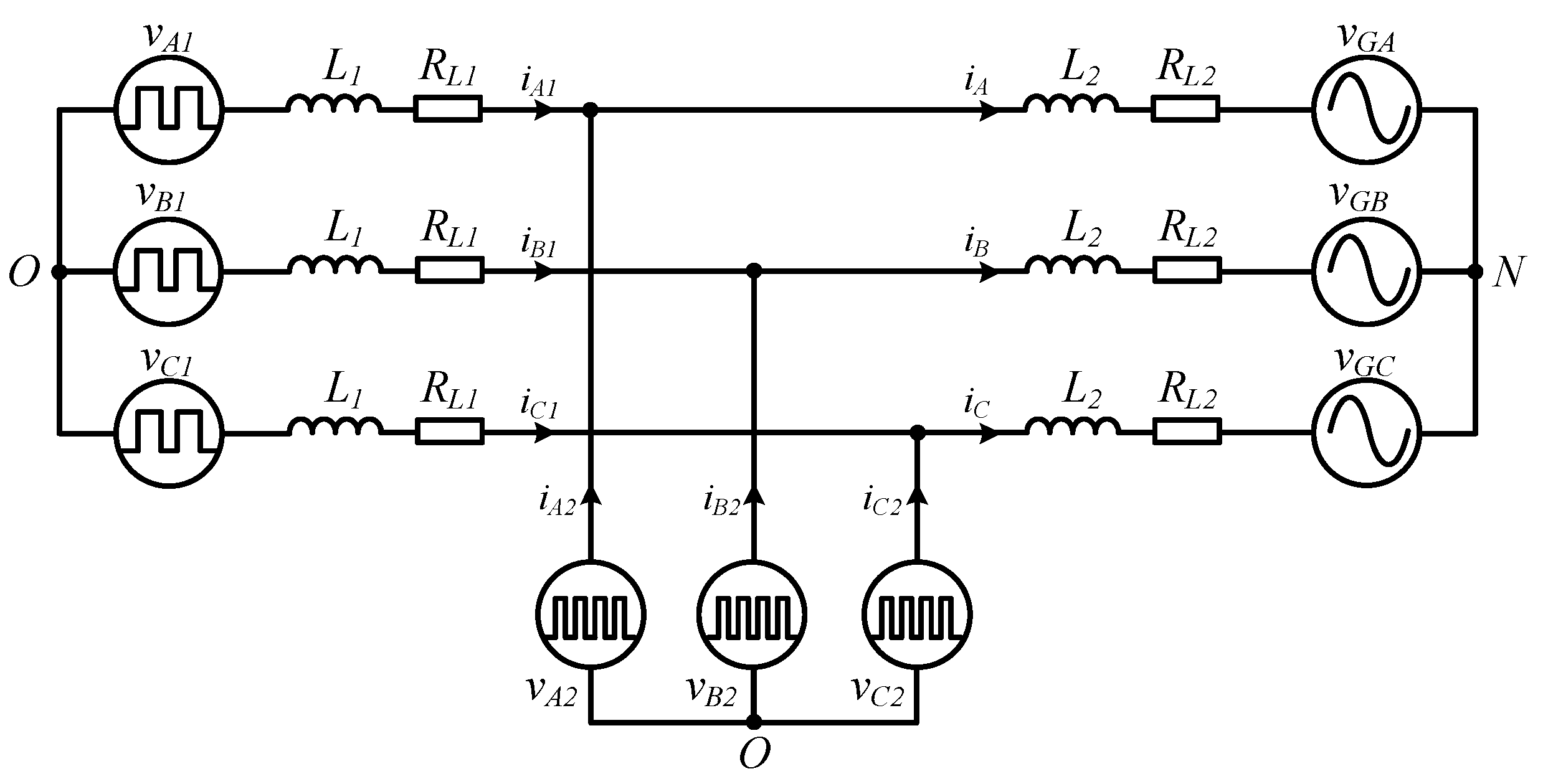
Before designing the current control strategy, it is necessary to explore the operation principle of current ripple compensation in this converter. Firstly, taking the grid-connected application as an example, the three-phase equivalent circuit of the proposed converter is derived as shown in Figure 2. In SPWM, the line-to-neutral voltage consists of the fundamental frequency component and the harmonic component by Fourier decomposition. Moreover, the harmonic component is primarily concentrated around the switching frequency, ignoring the effects of dead-time, device nonlinear characteristics, and other factors.
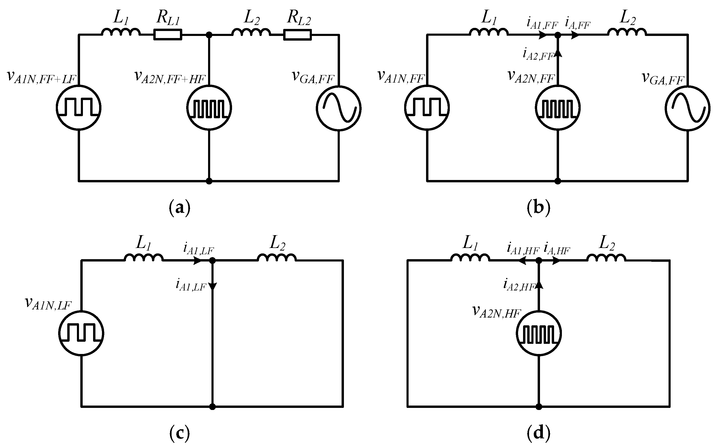
To improve readability, the equivalent circuits at different frequency ranges are derived as shown in Figure 3, taking phase A as an example. In Figure 3a, for the full frequency range, the line-to-neutral voltages can be expressed.
v A 1 N = v A 1 N , F F + v A 1 N , L F
v A 2 N = v A 2 N , F F + v A 2 N , H F
where VA1N represents the line-to-neutral voltage of the Si arm, VA1N,FF represents its fundamental frequency component, and VA1N,LF represents its harmonic component. Similarly, VA2N represents the line-to-neutral voltage of the SiC arm, VA2N,FF represents its fundamental frequency component, and VA2N,HF represents its harmonic component. In practical applications, it is assumed that ωL1 >> RL1 and ωL2 >> RL2. Thus, the resistance value of the filter inductors is allowed to be neglected. In Figure 3b, at the fundamental frequency, the Si arm current and grid current can be expressed.
i A 1 , F F = 1 L 1 ( v A 1 N , F F v A 2 N , F F ) d t
i A , F F = 1 L 2 ( v A 2 N , F F v G A , F F ) d t
where vGA,FF represents the grid voltage. In Figure 3c, since the switching frequency of the SiC arm is much higher than that of the Si arm, the SiC arm has no harmonic voltage at the LF range. The LF current ripple generated by the Si arm harmonic voltage can be expressed.
i A 1 , L F = 1 L 1 v A 1 N , L F d t
The SiC arm is equivalent to a short circuit for the LF current ripple, preventing it from flowing into the grid. In Figure 3d, the HF harmonic voltage of the Si arm can be disregarded, so the HF harmonic current is only generated by the SiC arm. Moreover, this HF current is insignificant compared to the FF and LF components. Thus, the Si arm current is approximately equal to the main FF current plus LF harmonic current.
i A 1 i A 1 , F F + i A 1 , L F
The SiC arm current is approximately equal to the compensated LF harmonic current plus fractional FF current.
i A 2 i A 1 , L F + i A 2 , F F
The grid current contains the FF component and the HF harmonic component.
i A = i A 1 , F F + i A 2 , F F + i A , H F
Therefore, the proposed converter has the potential for high power quality.
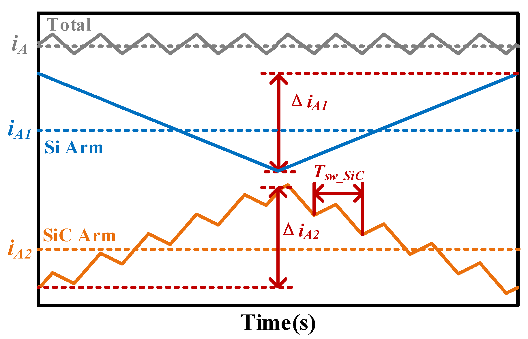
Based on the above analysis, the schematic diagram of current ripple compensation waveforms is given in Figure 4. It is assumed that the average current value remains constant within one Si arm switching period Tsw_Si. In order to reduce cost and volume, the inductance value L1 is minimized as much as possible. Meanwhile, the switching frequency of the Si arm is decreased to reduce losses, resulting in a large LF current ripple, as shown by the blue solid line in Figure 4. By appropriate current control strategy, the SiC arm operates at HF to compensate the Si arm current ripple and process the minor power, as shown by the yellow solid line in Figure 4. The current ripple of the SiC arm consists of two components. The first is the LF component, which is opposite to that of the Si arm. The second is the HF component, which is generated by the own HF switching events. As shown in the gray solid line in Figure 4, the total current ripple only has the HF component, which is determined only by the SiC arm and has nothing to do with the Si arm, achieving complete LF component compensation. Because of the high switching frequency of the SiC arm, the inductance value L2 is smaller than L1. The volume of inductors can be reduced while enhancing power quality.
In Figure 4, the dotted lines represent the average values corresponding to the solid lines. Since the Si and SiC arms share the output power, the average current relationships can be derived as follows.
M _ i A 1 = K M _ i A
M _ i A 2 = ( 1 K ) M _ i A
where M_iA1, M_iA2, and M_iA represent the Si arm average current, the SiC arm average current, and the total average current, respectively. K (0 < K < 1) represents the major power-sharing ratio. The current ripple ratio of the Si arm rA1 is defined by the following formula.
r A 1 = Δ i A 1 / M _ i A 1
where ΔiA1 represents the maximum peak-to-peak current ripple of the Si arm in one FF period. Since the SiC arm completely compensates the LF ripple, the following equation holds true.
Δ i A 2 = Δ i A 1
During this LF switching period, the peak current of the Si arm iA1,peak can be expressed.
i A 1 , p e a k = M _ i A 1 + 1 2 Δ i A 1
To avoid the circulating current in the SiC arm, iA1,peak should be less than the average value of the total current. Thus, the range of major power-sharing ratio K is limited by the following inequalities.
0 < K < 1 1 + r A 1 / 2

3. Proposed Current Control Strategy

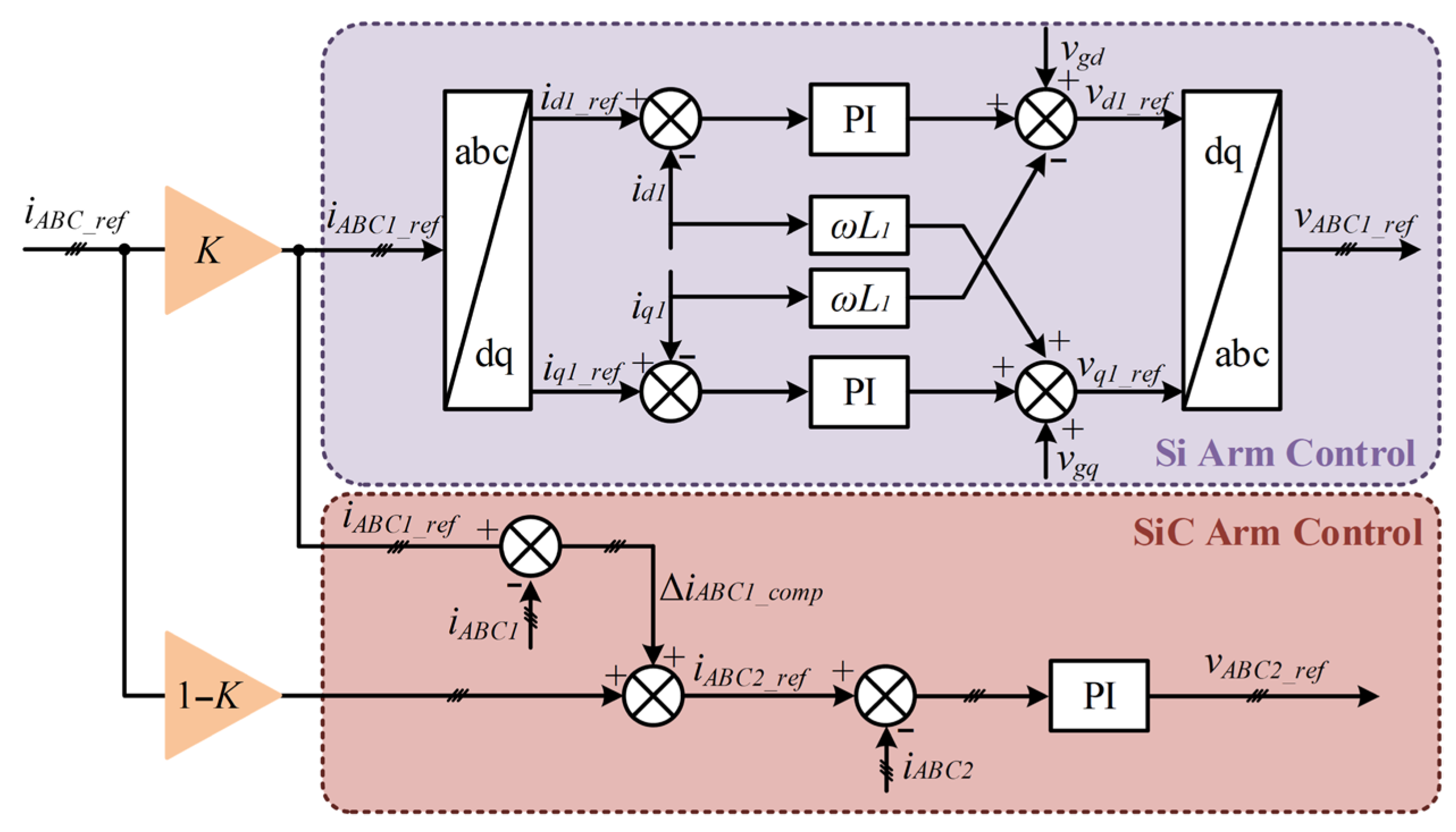
In this section, the closed-loop cooperative current control strategy is proposed to realize unequal current sharing and complete LF current ripple compensation. The block diagram of the control strategy is shown in Figure 5, which consists of two parts: the Si arm control loop (purple box) and the SiC arm control loop (red box). The following provides a detailed explanation of these two parts.

3.1. Si Arm Current Control

According to the control objective, the Si arm processes the main power. The major power sharing ratio K is used to generate the three-phase reference value of the Si arm current.
i A B C 1 _ r e f = K i A B C _ r e f
where iABC_ref is the three-phase reference value of the total current, which is usually determined by the target output power. The current distribution in the Si arm can be adjusted by modifying the parameter K, enabling flexible power-sharing capabilities. Considering the reference value is the FF current, the control loop is designed in the dq-frame, rotating with the grid angular frequency ω0. To enhance the dynamic response and disturbance resistance of the system, the grid voltage vg is used for feed-forward control. The traditional proportional-integral (PI) controller is used to achieve no-static-error tracking of FF current. The proportional gain Kp is designed to achieve the desired closed-loop bandwidth. Applying the magnitude condition (0 dB gain at the crossover frequency fc) leads to the dominant relationship Kp ≈ 2πfcL, ensuring fast dynamic response. The integral gain Ki is designed to shape the phase margin. By setting the zero frequency fz of the PI controller, we can compensate for the phase lag introduced by the plant’s pole, following Ki = Kp⋅2πfz, guaranteeing stability and robustness. The Si arm controller proportional coefficient Kp1 and the integral coefficient Ki1 are designed as follows.
K p 1 = 2 π f c 1 L 1
K i 1 = 2 π f z 1 K p 1
where the control bandwidth fc1 and integral corner frequency fz1 can be designed as follows.
f c 1 f s w _ S i 10 f s w _ S i 5
f z 1 = f c 1 10 f c 1 5
where fsw_Si is the switching frequency of the Si arm. In order to increase the control stability, the control period is equal to the switching period of the SiC arm. Therefore, the updating frequency of the Si arm reference voltage is equal to fsw_SiC, while the carrier frequency is equal to fsw_Si.

3.2. SiC Arm Current Control

The control objective of the SiC arm is to compensate for the LF ripple current and process the minor power. Thus, the SiC arm three-phase current reference can be divided into two parts. The LF ripple current generated by the Si arm can be expressed.
Δ i A B C _ c o m p = i A B C 1 _ r e f i A B C 1
Thus, the three-phase current reference of the SiC arm can be expressed.
i A B C 2 _ r e f = ( 1 K ) i A B C _ r e f + Δ i A B C _ c o m p
Considering the reference value consists of the FF and LF current, the control loop is designed in the abc-frame. Similarly, the PI controller is selected to track the FF and LF ripple current. The SiC arm controller proportional coefficient Kp2 and the integral coefficient Ki2 are designed as follows.
K p 2 = 2 π f c 2 L 2
K i 2 = 2 π f z 2 K p 2
where the control bandwidth fc2 and integral corner frequency fz2 can be designed as follows.
f c 2 f s w _ S i C 10 f s w _ S i C 5
f z 2 = f c 2 10 f c 2 5
where fsw_SiC is the switching frequency of the SiC arm.

4. Simulation Verification

In this section, a three-phase Si and SiC hybrid arms ANPC converter based on the cooperative current control strategy is simulated in PLECS (4.8.9) software, considering its extremely fast simulation speed and unique thermal analysis function. The parameters of the simulation system are provided in Table 1. The results of performance comparison between the proposed topology and existing typical topologies are also presented.
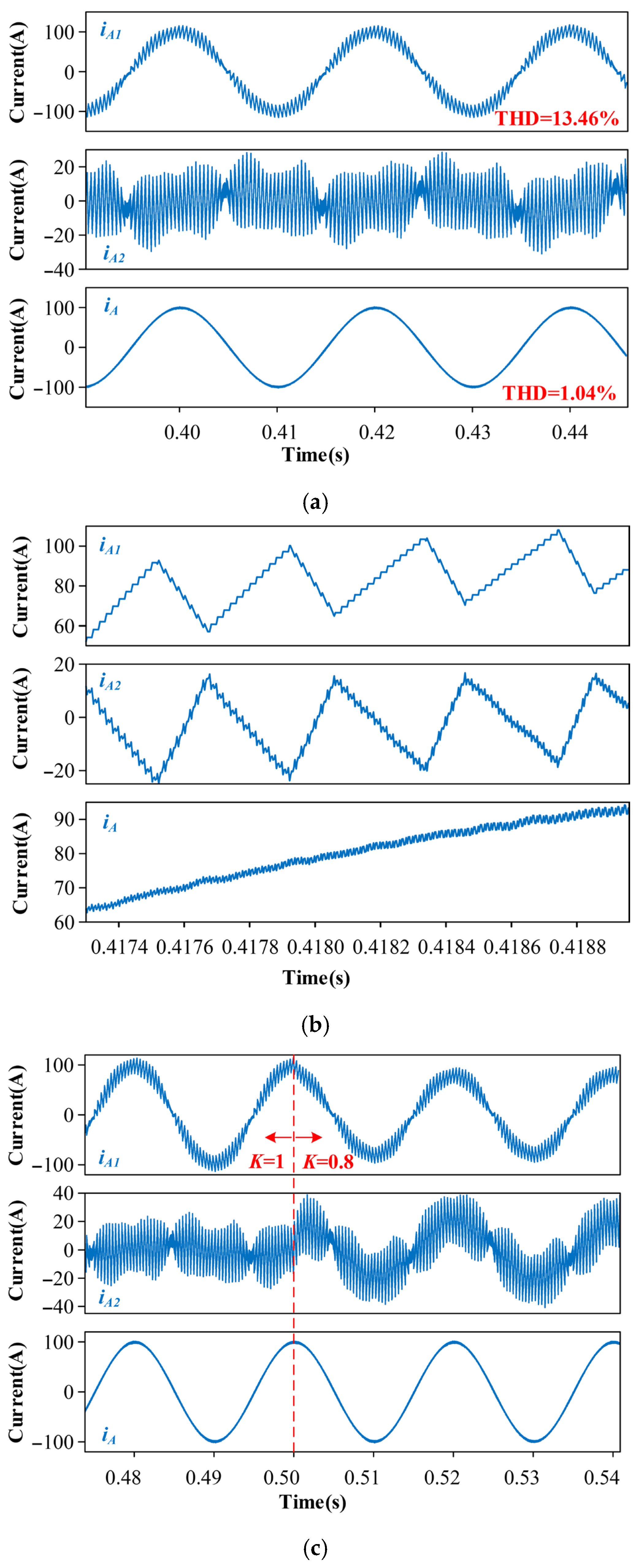
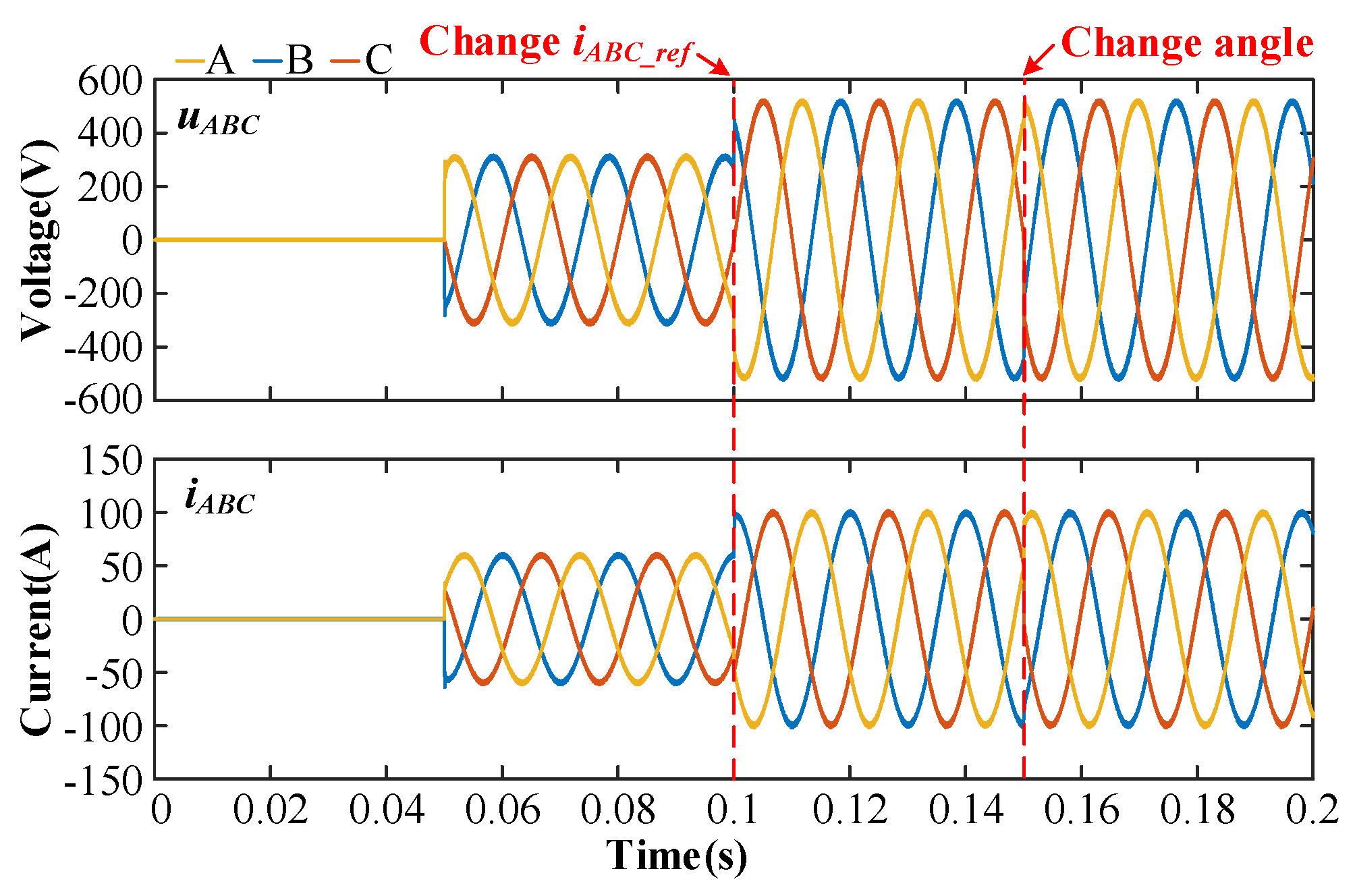
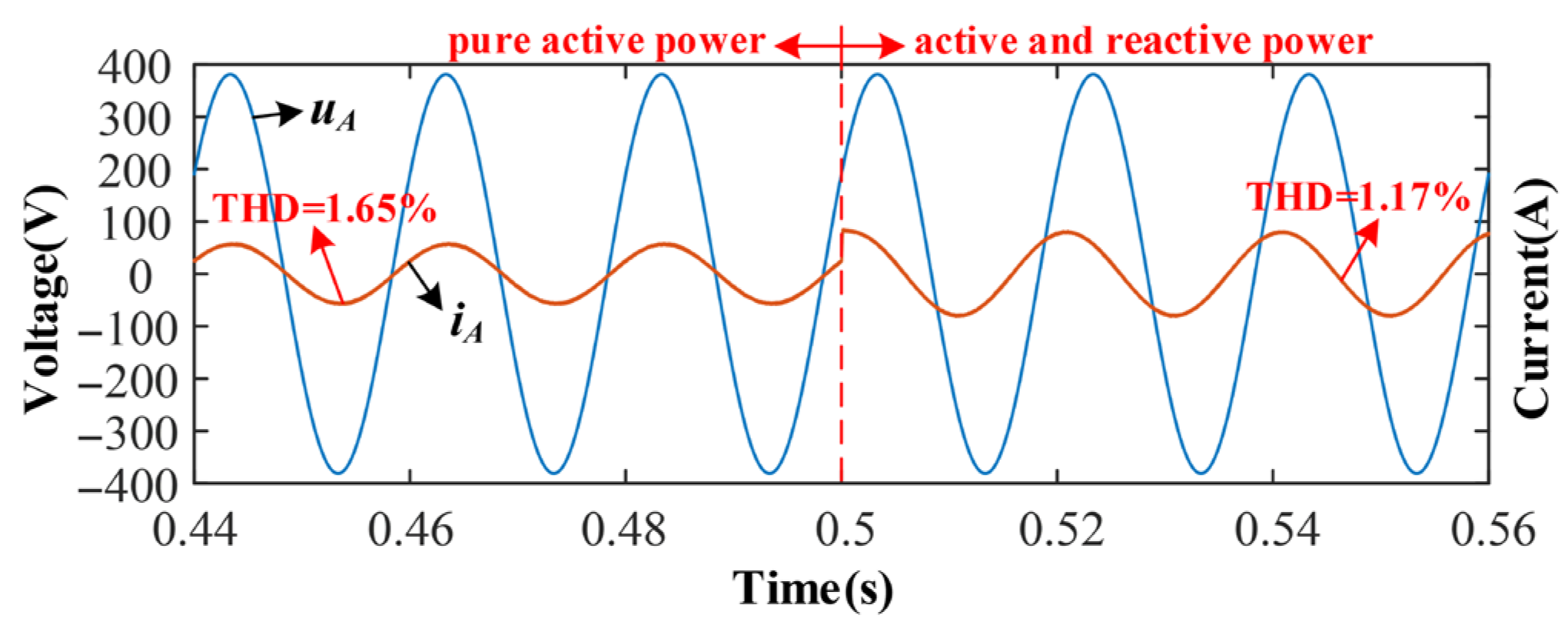
Taking phase-A as an example, the simulation waveforms of the Si arm current, the SiC arm current, and the total current are displayed in Figure 6. The results are consistent with the theoretical analysis. As can be seen in Figure 6a, the Si arm generates a large current ripple because of the low switching frequency, and the total harmonic distortion (THD) is 13.46%. Under the condition K = 1, the SiC arm only compensates the LF current ripple. By employing the proposed current control strategy, the THD of the total current is reduced to 1.04%. Figure 6b shows the detailed waveforms of the current ripple compensation. It can be concluded that the SiC arm can completely compensate for the LF ripple current generated by the Si arm, and the total current only includes the FF and HF ripple components. It can be seen from Figure 6c, when K changes from 1 to 0.8, the good power quality can be maintained while the circulating current between the Si and SiC arms can be reduced. The three-phase voltage and current waveforms are shown in Figure 7. At t = 0.1 s, the reference value of the three-phase current iABC_ref changes from 70 to 100. At t = 0.15 s, the cosine value of the angle reference changes from 1 to 0.8. It can be concluded that the proposed converter can achieve high control dynamics for the step changes in the current reference and angle reference. A grid-connected operation case where the converter undergoes a step change from outputting pure active power to combined active and reactive power is presented in Figure 8. It can be demonstrated that the proposed control strategy exhibits excellent transient performance with rapid dynamic response, while maintaining superior power quality both before and after the transition period.

5. Experimental Results

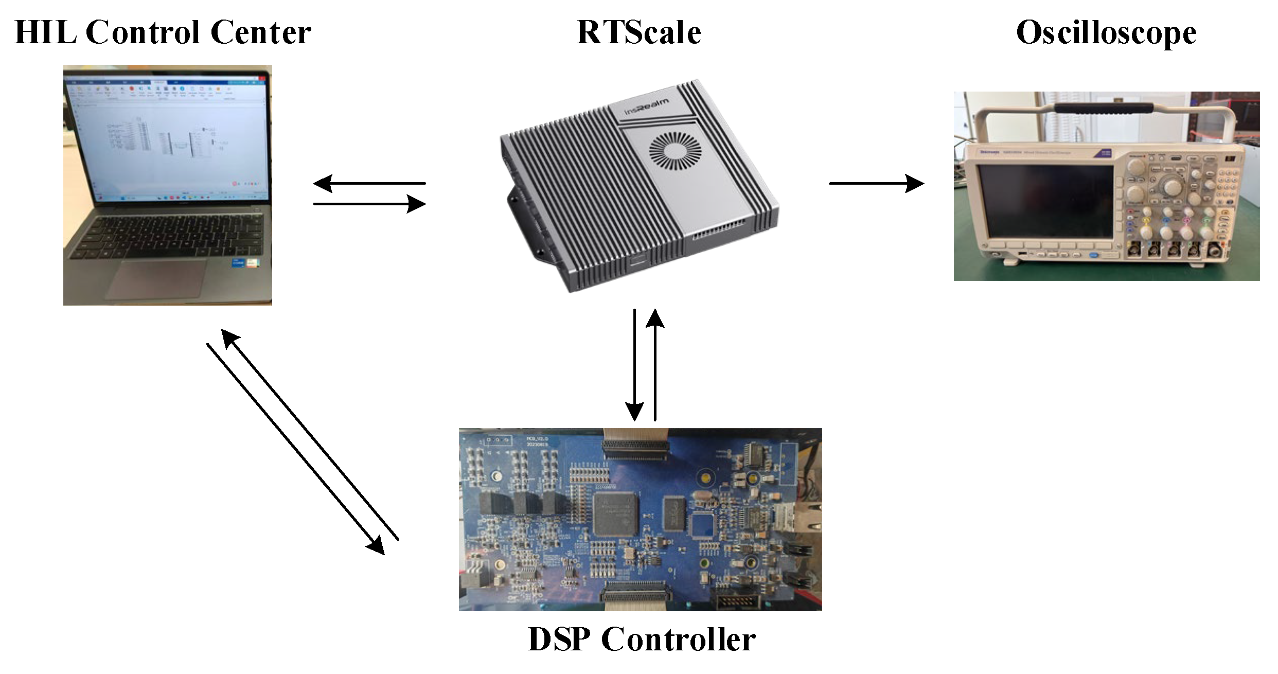
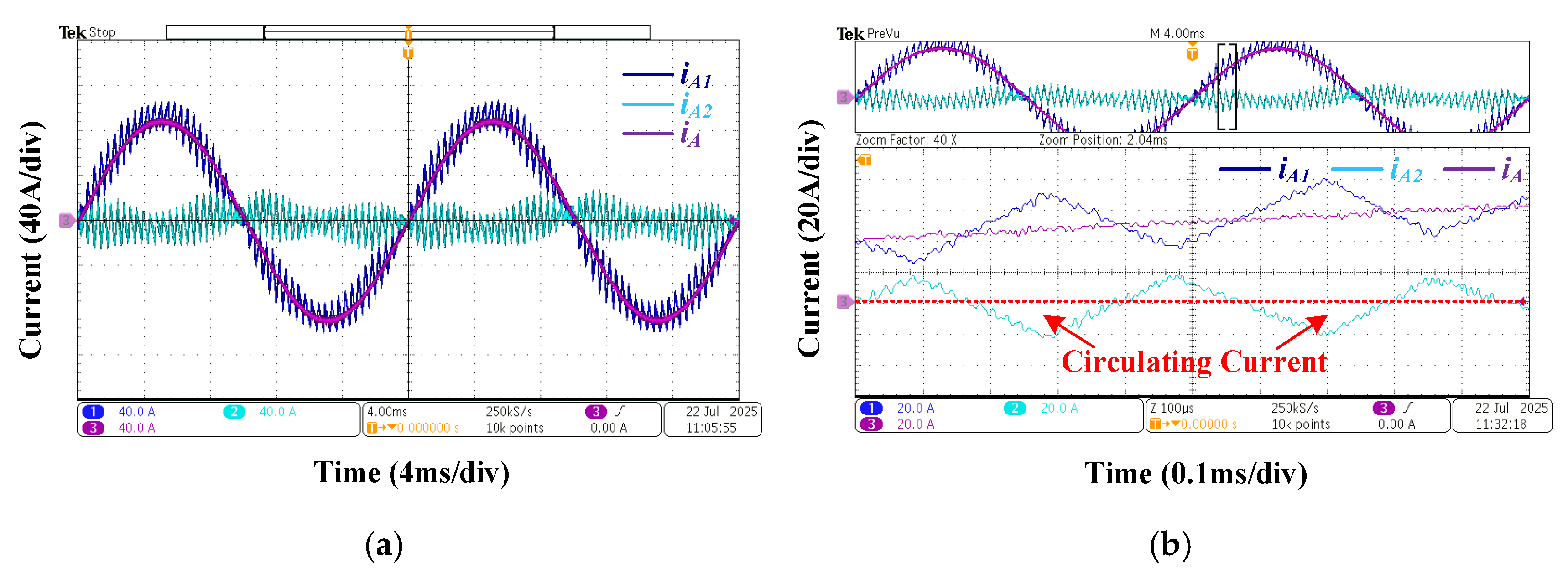
To further verify the effectiveness of the proposed closed-loop cooperative current control strategy, experiments are carried out on a hardware-in-loop platform, as shown in Figure 9. The controller is implemented by a DSP (TMS320F28377D) control system. The power part of the proposed converter is simulated by the RTScale real-time simulator. Critical waveforms were captured and analyzed using a high-bandwidth digital oscilloscope, ensuring accurate measurement of dynamic performance and power quality. Due to the symmetry of the circuit, the waveforms of current in phase A are selected for presentation. The steady-state experimental waveforms of the current under iABC_ref = 90 A and K = 1 are presented in Figure 10. It can be seen from Figure 10a that the Si arm processes the total load current while generating a considerable ripple current due to the reduced switching frequency. Under this condition, the SiC arm only compensates the LF ripple current. It can be seen from Figure 10b that the LF ripple current is eliminated, but there is a circulating current between the Si and SiC arms, leading to additional power losses. The steady-state experimental waveforms of the current under iABC_ref = 90 A and K = 0.7 are presented in Figure 11. It can be seen from Figure 11a that the SiC arm compensates the LF ripple current while sharing minor load current. It can be seen from Figure 11b that there is no circulating current between the Si and SiC arms by adjusting the major power sharing ratio K. It can be concluded from Figure 10 and Figure 11 that the flexible power sharing and complete ripple current compensation can be realized by employing the proposed current control strategy. Meanwhile, because of the extremely high equivalent switching frequency, the excellent power quality of the output total current can be achieved. It can also be maintained regardless of changing K.
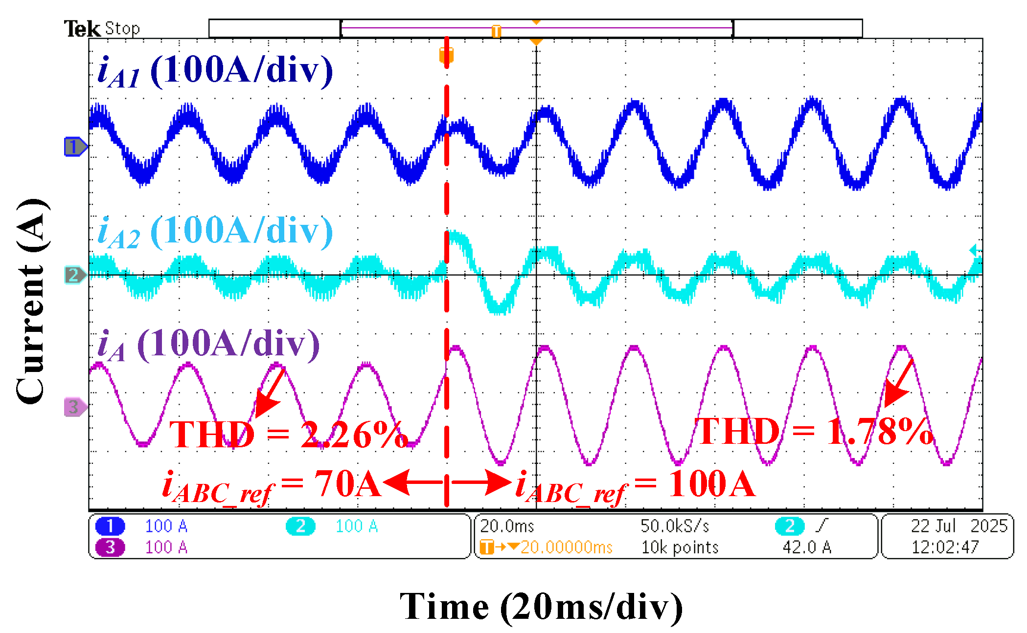
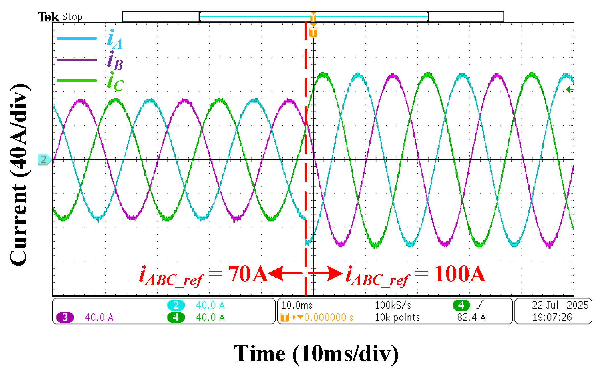
Furthermore, the dynamic waveforms of the current while K changes from 1 to 0.7 are presented in Figure 12. During the dynamic process of changing the power sharing ratio, there are no fluctuations occurring in the total output current. This provides the possibility of adjusting the optimal K under different operation conditions. Figure 13 shows the dynamic experimental waveforms of the current while iABC_ref changes from 70 A to 100 A. It can be found that the high control dynamics for the step changes in the current reference can be achieved. When the load power is changed, the steady-state current sharing between the Si and SiC arms can remain unchanged. The dynamic changes in the current sharing between the Si and SiC do not affect the total output current. The dynamic experimental waveforms of the line-to-neutral current while changing the current reference are presented in Figure 14. It can be found that the proposed current control can be applied effectively in the three-phase circuits.

6. Performance Comparison

6.1. Cost Comparison

To prove the cost-effectiveness of the proposed converter, the all-SiC and all-Si 3L-ANPC topologies are chosen for comparison. Considering the DC bus voltage is 800 V, the 650 V voltage rating Si IGBTs or SiC MOSFETs are selected to configure the all-SiC or all-Si topologies. For the proposed hybrid arms converter, Si IGBTs S1S6 select the 650 V voltage rating devices, while SiC MOSFETs S7S8 select the 1200 V voltage rating and smaller current rating devices. For a fair comparison, the filter inductors of the three topologies are selected to have the same inductance value. It should be considered that the proposed converter uses one more driver chip and current sensor in each phase than the all-SiC and all-Si converters. The chosen components and total price for each phase of three topologies are summarized in Table 2. The unit price of each component is taken from www.mouser.com, accessed on 10 October 2025. It can be found that, compared to the all-SiC converter, the proposed converter can achieve more than 60% total cost reduction.

6.2. Efficiency Comparison

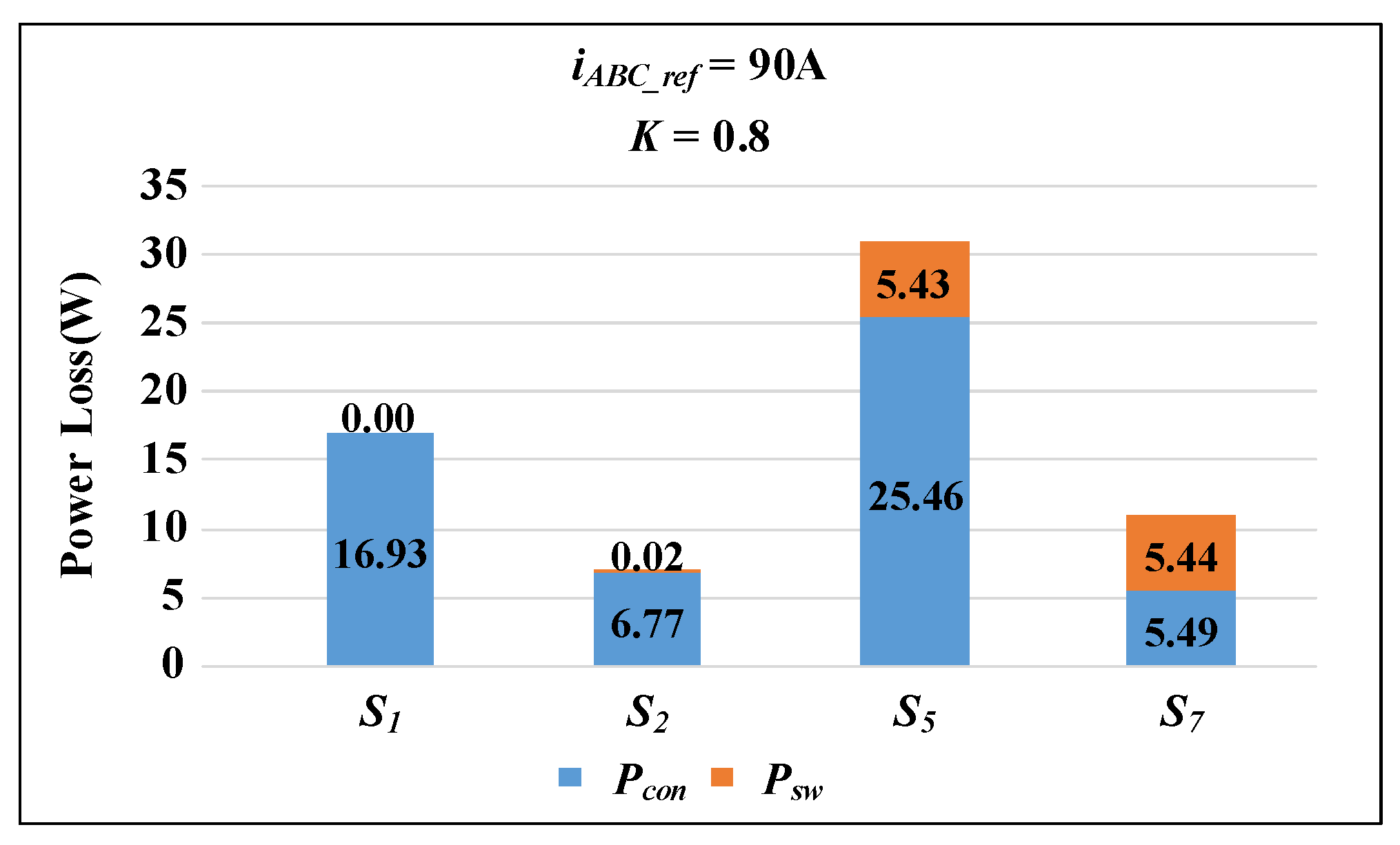
To evaluate the efficiency performance of the proposed converter, the thermal model was created in the PLECS software environment. The power losses distribution of the proposed converter under iABC_ref = 90 A and K = 0.8 is presented in Figure 15. Due to the symmetry of the circuit, only half of the devices are presented. According to the results, the FF Si IGBTs S1 and S2 have almost no switching losses. The LF Si IGBT S5 has very little switching loss because of reduced switching frequency. The power losses of the HF SiC MOSFET S7 are very low due to its excellent switching characteristics. The results are consistent with the designed modulation scheme. Meanwhile, the power-sharing ratio between the Si and SiC arms can seriously affect the efficiency performance. Therefore, the proper selection of the major power sharing ratio K is very important for the efficiency optimization. In Figure 16, the relationship curve between the major power sharing ratio K and power losses under iABC_ref = 90 A is presented. From this curve, the optimal K under this operating condition can be obtained. In Figure 17, the junction temperature of the devices under different major power sharing ratio K with iABC_ref = 90 A is presented. It can be found that a key feature of our control strategy is the optimization of temperature equilibrium between the Si and SiC devices via adjusting K. This active balancing prevents localized overheating in any single SiC device, thereby directly countering the temperature-activated mechanisms of gate oxide degradation and threshold voltage drift.
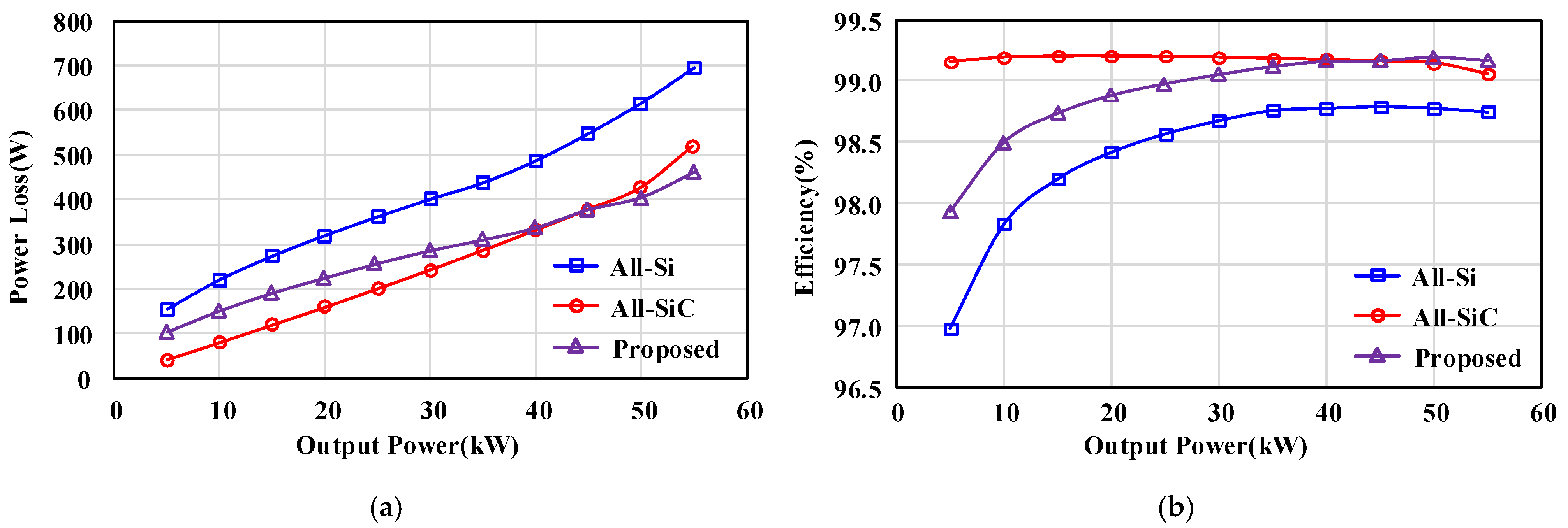
The all-SiC and all-Si 3L-ANPC converters are also chosen for the efficiency comparison. To ensure fairness, the three converters select the same value of filter inductance. Thus, the filter inductance values for all-SiC and all-Si converters are both 1.5 mH. The same modulation scheme is applied in the three converters. Moreover, the switching frequencies of all-SiC and all-Si converters are decided by the THD of the output current, which should be almost equal to that of the proposed converter. Based on the abovementioned conditions, the comparison results are fair and persuasive. In Figure 18, the simulated power losses and efficiency comparisons under different output power are presented. It can be found that the all-Si ANPC converter has the highest power losses. The proposed hybrid arms ANPC converter can achieve 30–40% power loss reduction compared to the all-Si converter in the full power range. In particular, under high-power operation conditions, the efficiency of the proposed converter is higher than that of the all-SiC ANPC converter. The reason is that Si IGBT has a lower conduction voltage than SiC MOSFET under large current conditions, leading to lower conduction losses. Meanwhile, the SiC arm processes the minor load current, which can fully leverage its advantages of low-switching-loss and low-conduction-loss under this condition. Therefore, the proposed topology fully leverages the respective advantages of Si IGBT and SiC MOSFET. It is more attractive than an all-SiC converter in many high-power industrial applications due to higher efficiency and lower cost.

7. Conclusions

In this paper, a Si and SiC hybrid arms ANPC converter combined with the hybrid-frequency modulation scheme and the WFPP concept was proposed. The advantages of the proposed converter can be concluded as follows.
(1)
The proposed converter uses smaller current rating SiC devices, which can achieve more than 60% total cost reduction compared to the all-SiC 3L-ANPC converter.
(2)
Although the switching frequency of Si devices is decreased to reduce power losses, the equivalent switching frequency is equal to that of the all-SiC design. Thus, excellent power quality can be achieved.
(3)
By employing the hybrid-frequency modulation scheme and proposed current control strategy, the proposed converter can reduce 30–40% power losses compared to the all-Si converter in the full power range. Moreover, the efficiency under high-current conditions is higher than that of the all-SiC design.
The proposed converter fully leverages the respective advantages of Si IGBT and SiC MOSFET, achieving the comprehensive optimization of power quality, efficiency, and cost. It is more attractive than an all-SiC converter in high-power industrial applications due to higher efficiency and lower cost. For extension to medium- and high-voltage applications (e.g., 10-kV grid-connected inverters), the proposed topology offers two clear paths for voltage scaling. On one hand, it can serve as a submodule in cascaded H-bridge (CHB) or the modular multilevel converter (MMC). On the other hand, direct series-connection of devices within each switch presents another viable route.

Author Contributions

Conceptualization, T.X. and C.L.; methodology, T.X.; software, T.X.; validation, T.X., X.F. and Z.A.; formal analysis, T.X. and C.L.; investigation, M.L.; resources, C.L. and H.L.; data curation, T.X. and X.F.; writing—original draft preparation, T.X.; writing—review and editing, X.F., Z.A. and C.L.; visualization, H.L.; supervision, H.Y.; project administration, C.L. and H.Y. All authors have read and agreed to the published version of the manuscript.

Funding

This research was funded by the National Key Research and Development Program of China, grant number 2025YFE0101600, and the Zhejiang Provincial Natural Science Foundation of China, grant number LR24E070001, and the Power Electronics Science and Education Development Program of Delta Group, grant number DREG2024001.

Data Availability Statement

The data presented in this study are available on request from the corresponding author.

Conflicts of Interest

The authors declare no conflicts of interest.

Abbreviations

The following abbreviations are used in this manuscript:
WBGWide bandgap
ANPCActive neutral-point-clamped
FFFundamental frequency
LFLow frequency
HFHigh frequency
MEAMore electric aircraft
WFPPWBG fractional power processing
HHBHybrid half-bridge
PFCPower factor correction
3LThree-level
5LFive-level

References

  1. Kouro, S.; Malinowski, M.; Gopakumar, K.; Pou, J.; Franquelo, L.G.; Wu, B.; Rodriguez, J.; Pérez, M.A.; Leon, J.I. Recent Advances and Industrial Applications of Multilevel Converters. IEEE Trans. Ind. Electron. 2010, 57, 2553–2580. [Google Scholar] [CrossRef]
  2. Blaabjerg, F.; Yang, Y.; Kim, K.A.; Rodriguez, J. Power Electronics Technology for Large-Scale Renewable Energy Generation. Proc. IEEE 2023, 111, 335–355. [Google Scholar] [CrossRef]
  3. Ali, A.; Mousa, H.H.H.; Shaaban, M.F.; Azzouz, M.A.; Awad, A.S.A. A Comprehensive Review on Charging Topologies and Power Electronic Converter Solutions for Electric Vehicles. J. Mod. Power Syst. Clean Energy 2024, 12, 675–694. [Google Scholar] [CrossRef]
  4. Wang, D.; Hemming, S.; Yang, Y.; Poorfakhraei, A.; Zhou, L.; Liu, C.; Emadi, A. Multilevel Inverters for Electric Aircraft Applications: Current Status and Future Trends. IEEE Trans. Transp. Electrif. 2024, 10, 3258–3282. [Google Scholar] [CrossRef]
  5. Kumar, R.; Singh, B.; Kant, P. Design and Analysis of a 54-Pulse Converter and 7-Level Hybrid Inverter for Medium Voltage Induction Motor Drive. IEEE Trans. Ind. Appl. 2023, 60, 560–572. [Google Scholar] [CrossRef]
  6. Millán, J.; Godignon, P.; Perpiñà, X.; Pérez-Tomás, A.; Rebollo, J. A Survey of Wide Bandgap Power Semiconductor Devices. IEEE Trans. Power Electron. 2014, 29, 2155–2163. [Google Scholar] [CrossRef]
  7. Zhang, Y.; Li, C.; Li, C.; Xin, Z.; Chen, R.; Li, W.; He, X.; Ma, H. A SiC and Si Hybrid Five-Level Unidirectional Rectifier for Medium Voltage Applications. IEEE Trans. Ind. Electron. 2022, 69, 7537–7548. [Google Scholar] [CrossRef]
  8. Cai, Y.; Sun, P.; Chen, C.; Zhang, Y.; Zhao, Z.; Li, X.; Qi, L.; Chen, Z.; Nee, H.-P. Investigation on Gate Oxide Degradation of SiC MOSFET in Switching Operation. IEEE Trans. Power Electron. 2024, 39, 9565–9578. [Google Scholar] [CrossRef]
  9. Jiang, H.; Qi, X.; Qiu, G.; Zhong, X.; Tang, L.; Mao, H.; Wu, Z.; Chen, H.; Ran, L. A Physical Explanation of Threshold Voltage Drift of SiC MOSFET Induced by Gate Switching. IEEE Trans. Power Electron. 2022, 37, 8830–8834. [Google Scholar] [CrossRef]
  10. Kang, M.; Yu, S.; Xing, D.; Liu, T.; Salemi, A.; Booth, K.; Zhu, S.; White, M.H.; Agarwal, A.K. Body Diode Reliability of Commercial SiC Power MOSFETs. In Proceedings of the 2019 IEEE 7th Workshop on Wide Bandgap Power Devices and Applications (WiPDA), Raleigh, NC, USA, 29–31 October 2019; pp. 416–419. [Google Scholar]
  11. Zhang, D.; He, J.; Pan, D. A Megawatt-Scale Medium-Voltage High-Efficiency High Power Density “SiC+Si” Hybrid Three-Level ANPC Inverter for Aircraft Hybrid-Electric Propulsion Systems. IEEE Trans. Ind. Appl. 2019, 55, 5971–5980. [Google Scholar] [CrossRef]
  12. Lei, Z.; Zhuge, H.; Lou, X.; Zhang, L.; Tao, J. Performance Comparison of 4-SiC and 2-SiC Hybrid Three-Phase Three-Level ANPC Inverters. In Proceedings of the 2021 IEEE Sustainable Power and Energy Conference (iSPEC), Nanjing, China, 23–25 December 2021; pp. 3204–3209. [Google Scholar]
  13. Li, C.; Guan, Q.; Lei, J.; Li, C.; Zhang, Y.; Wang, S.; Xu, D.; Li, W.; Ma, H. An SiC MOSFET and Si Diode Hybrid Three-Phase High-Power Three-Level Rectifier. IEEE Trans. Power Electron. 2019, 34, 6076–6087. [Google Scholar] [CrossRef]
  14. Zhang, L.; Zheng, Z.; Li, C.; Ju, P.; Wu, F.; Gu, Y.; Chen, G. A Si/SiC Hybrid Five-Level Active NPC Inverter with Improved Modulation Scheme. IEEE Trans. Power Electron. 2020, 35, 4835–4846. [Google Scholar] [CrossRef]
  15. Zhang, Y.; He, J.; Padmanaban, S.; Ionel, D.M. Transistor-Clamped Multilevel H-Bridge Inverter in Si and SiC Hybrid Configuration for High-Efficiency Photovoltaic Applications. In Proceedings of the 2018 IEEE Energy Conversion Congress and Exposition (ECCE), Portland, OR, USA, 23–27 September 2018; pp. 2536–2542. [Google Scholar]
  16. Belkhode, S.; Shukla, A.; Doolla, S. Five-Level Hybrid Active-NPC H-Bridge Converter with Novel Space-Vector-Modulation Scheme. IEEE J. Emerg. Sel. Top. Power Electron. 2022, 10, 4146–4159. [Google Scholar] [CrossRef]
  17. Endres, J.; Ackva, A. A Parallel Three-Phase Converter System for Ripple Current Compensation and Passive Filter Reduction. In Proceedings of the 2015 17th European Conference on Power Electronics and Applications (EPE’15 ECCE-Europe), Geneva, Switzerland, 8–10 September 2015; pp. 1–9. [Google Scholar]
  18. Kundu, A.; Na, R.; Amir, A.; Zhou, Y.; Brown, I.P.; John Shen, Z. WBG Fractional Power Processing: A New Si-SiC Hybrid Voltage Source Inverter Design. In Proceedings of the 2020 IEEE Energy Conversion Congress and Exposition (ECCE), Detroit, MI, USA, 11–15 October 2020; pp. 6226–6231. [Google Scholar]
  19. Kundu, A.; Na, R.; Amir, A.; Shen, Z.J. Optimization Strategy of WBG Fractional Power Processing. In Proceedings of the 2021 IEEE Applied Power Electronics Conference and Exposition (APEC), Phoenix, AZ, USA, 14–17 June 2021; pp. 896–901. [Google Scholar]
  20. Zhang, C.; Wang, J.; Qu, K.; Hu, B.; Li, Z.; Yin, X.; Shen, Z.J. WBG and Si Hybrid Half-Bridge Power Processing Toward Optimal Efficiency, Power Quality, and Cost Tradeoff. IEEE Trans. Power Electron. 2022, 37, 6844–6856. [Google Scholar] [CrossRef]
  21. Zhang, C.; Qu, K.; Hu, B.; Wang, J.; Yin, X.; Shen, Z.J. A High-Frequency Dynamically Coordinated Hybrid Si/SiC Interleaved CCM Totem-Pole Bridgeless PFC Converter. IEEE J. Emerg. Sel. Top. Power Electron. 2022, 10, 2088–2100. [Google Scholar] [CrossRef]
  22. Zhang, C.; Yuan, X.; Wang, J.; Hu, B.; Yin, X.; Shen, Z.J. Optimization of Power Sharing and Switching Frequency in Si/WBG Hybrid Half-Bridge Converters Using Power Loss Models. IEEE J. Emerg. Sel. Top. Power Electron. 2023, 11, 2837–2849. [Google Scholar] [CrossRef]
  23. Zhang, C.; Yuan, X.; Wang, J.; Chen, W.; Hu, B.; Shen, Z.J. Adaptive Power Sharing and Switching Frequency Control for Power Loss Optimization in WBG/Si Hybrid Half-Bridge Converters. IEEE Trans. Power Electron. 2023, 38, 4440–4450. [Google Scholar] [CrossRef]
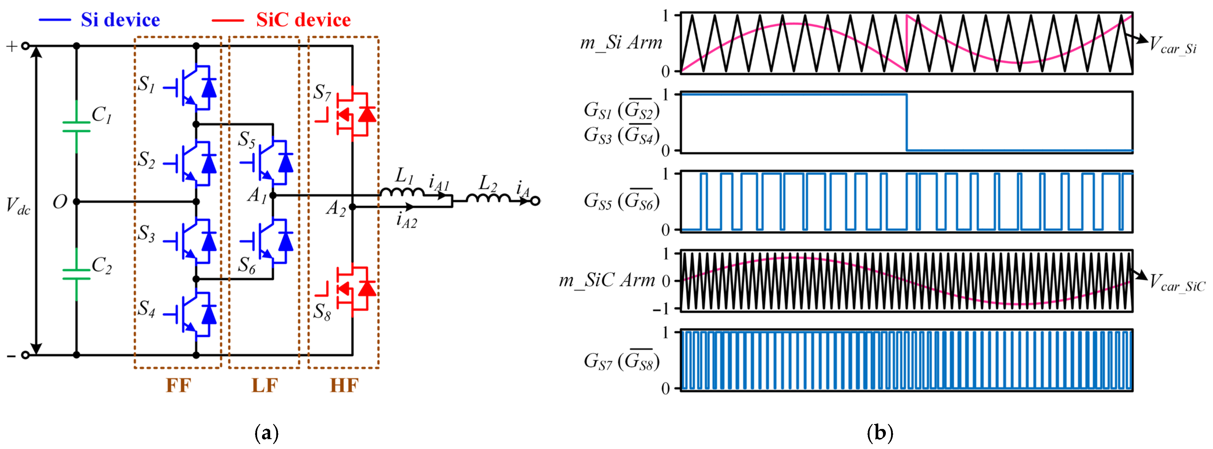
Figure 1. Topology and modulation scheme of the proposed converter. (a) The per-phase circuit; (b) Waveforms of the modulation scheme.
Energies 18 06198 g001
Figure 2. Three-phase equivalent circuit of the proposed converter for grid-connected application.
Energies 18 06198 g002
Figure 3. Single-phase equivalent circuit at different frequency ranges. (a) Full frequency range; (b) Fundamental frequency; (c) Si arm switching frequency; (d) SiC arm switching frequency.
Energies 18 06198 g003
Figure 4. Schematic diagram of current ripple compensation waveforms.
Energies 18 06198 g004
Figure 5. Block diagram of the proposed cooperative current control strategy.
Energies 18 06198 g005
Figure 6. Simulation waveforms of the Si arm current, the SiC arm current, and total current in phase A. (a) Steady-state waveforms under K = 1; (b) Detailed waveforms of current ripple compensation under K = 1; (c) Waveforms of K changing from 1 to 0.8.
Energies 18 06198 g006
Figure 7. Simulation waveforms of line-to-line voltage and line-to-neutral current for step changes in the current reference and angle reference.
Energies 18 06198 g007
Figure 8. Simulation waveforms of grid-side voltage and current in phase A.
Energies 18 06198 g008
Figure 9. Hardware-in-loop experiment platform.
Energies 18 06198 g009
Figure 10. Experimental waveforms of the current in phase A under iABC_ref = 90 A and K = 1. (a) Steady-state waveforms of the Si arm current, the SiC arm current, and the total current; (b) Detailed waveforms of current ripple compensation.
Energies 18 06198 g010
Figure 11. Experimental waveforms of the current in phase A under iABC_ref = 90 A and K = 0.7. (a) Steady-state waveforms of the Si arm current, the SiC arm current, and the total current; (b) Detailed waveforms of current ripple compensation.
Energies 18 06198 g011
Figure 12. Experimental waveforms of the current in phase A under iABC_ref = 90 A while K changes from 1 to 0.7.
Energies 18 06198 g012
Figure 13. Experimental waveforms of the current in phase A under K = 0.7 while iABC_ref changes from 70 A to 100 A.
Energies 18 06198 g013
Figure 14. Experimental waveforms of the line-to-neutral current while iABC_ref changes from 70 A to 100 A.
Energies 18 06198 g014
Figure 15. Power losses distribution of the proposed converter under iABC_ref = 90 A and K = 0.8.
Energies 18 06198 g015
Figure 16. Relationship curve between the major power sharing ratio K and power losses under iABC_ref = 90 A.
Energies 18 06198 g016
Figure 17. The junction temperature of the devices under different major power sharing ratio K with iABC_ref = 90 A.
Energies 18 06198 g017
Figure 18. The comparison results of power losses and efficiency under different output power. (a) Power losses comparison results; (b) Efficiency comparison results.
Energies 18 06198 g018
Table 1. Simulation parameters.
ParameterValue
DC Bus Voltage Vdc800 V
Fundamental Frequency fb50 Hz
Si Arm Switching Frequency fsw_Si2.5 kHz
SiC Arm Switching Frequency fsw_SiC50 kHz
Si Arm Filter Inductance L11 mH
SiC Arm Filter Inductance L2500 μH
Load Resistor Rload3 Ω
Table 2. Chosen components and cost comparison.
ComponentsAll-SiCAll-SiProposed
SiC MOSFETC3M0015065K
($35.20 × 6)
/C3M0040120K1
($11.19 × 2)
Si IGBT/IKZ75N65EL5
($4.01 × 6)
IKZ75N65EL5
($4.01 × 6)
Driver ICUCC21732
($2.22 × 3)
UCC21732
($2.22 × 3)
UCC21732
($2.22 × 4)
Current SensorCASR 50-NP
($9.92 × 1)
CASR 50-NP
($9.92 × 1)
CASR 50-NP
($9.92 × 1)
CASR 15-NP
($9.06 × 1)
Total Cost$227.78$40.64$74.3
Disclaimer/Publisher’s Note: The statements, opinions and data contained in all publications are solely those of the individual author(s) and contributor(s) and not of MDPI and/or the editor(s). MDPI and/or the editor(s) disclaim responsibility for any injury to people or property resulting from any ideas, methods, instructions or products referred to in the content.