Abstract
In order to reduce magnetic components for a current-fed dual active bridge converter, this paper proposes a dual coupled-inductor (DCI) structure, which integrates two DC inductors, one high-frequency transformer, and one leakage inductor into two EE cores. By analyzing the principle of the magnetic components, a derivation process is presented to modify the current-fed dual active bridge converter. To simplify the design and enhance efficiency, an equal air gap length optimization method is proposed. And the geometric parameters with the highest efficiency are optimized based on losses. Finally, the feasibility and effectiveness of the above design were verified through a 1 kW test prototype.
1. Introduction
Energy storage systems have become an indispensable core component of modern power systems, widely used in key areas [1] such as sustainable energy power systems, microgrids, electric vehicle drive systems, and uninterruptible power supplies (UPS). In these applications, energy storage units such as batteries and supercapacitors typically need to be connected to high-voltage DC buses [2,3] through power electronic conversion devices to achieve efficient, bidirectional flow of energy. Among them, the current-fed dual active bridge (CF-DAB) DC–DC converter [4,5,6,7] is widely regarded as one of the ideal choices for achieving this connection function due to its outstanding advantages, such as low input current ripple, wide voltage gain range, and effective support for bidirectional energy flow. It plays a key role in improving the overall efficiency and dynamic response performance of the system.
However, despite the many advantages of CF-DAB, there are still some significant bottlenecks in its practical engineering applications. Firstly, in order to achieve soft switching characteristics and maintain system stability, traditional CF-DAB topology typically requires the configuration of multiple independent magnetic components, such as input-side DC filtering inductors, isolation transformers, and auxiliary inductors for energy regulation [8]. These discrete components not only significantly increase the volume and weight of the system, resulting in a decrease in power density, but also cause additional copper and core losses due to the dispersed layout of magnetic components, limiting further improvement in overall efficiency. Especially in application scenarios such as electric vehicles and portable energy storage that have strict requirements for both volume and efficiency, the above issues become particularly prominent.
Currently, in order to achieve the operational goals of high-power density and high efficiency in the system, researchers generally adopt magnetic component integration technology as the main technical path [9,10,11,12,13]. For example, previous studies have significantly reduced the volume and number of magnetic components by coupling two DC inductors on the low-voltage side and integrating them into a single magnetic core [14,15], or further integrating the DC inductors with a high-frequency transformer into a multiwinding coupled-inductor structure [16,17]. In addition, in order to reduce the manufacturing cost and process complexity of magnetic components, existing solutions usually adopt a flat printed circuit board (PCB) winding, namely planar magnetic technology [18,19]. However, these methods still have a common limitation: they have not achieved internal integration of the leakage inductor and still rely on external series inductors to meet the leakage inductor requirement, which not only increases system volume but also restricts further improvement of power density. To further reduce the number of magnetic components, reference can be made to the leakage inductor integration method adopted in [20,21,22]. Ref. [20] can achieve controllable leakage inductance by introducing a magnetic shunt, which offers moderate control accuracy. However, the introduction of this additional component increases manufacturing complexity and cost. Ref. [21] can achieve the controllability of leakage inductance by adjusting the spatial distance. Although compared to [20], this method does not add additional magnetic components and has a moderate manufacturing complexity, the calculation is complex, and it is sensitive to mechanical accuracy, resulting in low inductance control accuracy and increased losses as the distance increases. Ref. [22] achieves controllable leakage inductance by adjusting the resistance, which has higher control accuracy compared to [21], but its complex winding structure limits manufacturing feasibility, and the energy consumption of the resistance leads to significant system losses.
In response to the limitations of traditional CF-DAB in terms of power density and efficiency, this paper proposes a dual coupled-inductor (DCI) structure. This structure integrates two DC inductors, one high-frequency transformer, and the required leakage inductor of the circuit into two EE magnetic cores. Compared with existing solutions, the DCI structure reduces the total volume and the occupied space of magnetic components while maintaining functional integrity, providing a new solution for the miniaturization and lightweighting of converters. In terms of parameter control, precise control of DC inductance and leakage inductance can be achieved by designing the number of PCB windings and the length of the magnetic core air gap reasonably. This design not only ensures the flexibility and adjustability of magnetic parameters but also enhances the adaptability to the dynamic performance of the converter. In addition, to further suppress leakage flux, reduce magnetic component losses, and improve the overall efficiency of the converter, this paper proposes a magnetic core optimization method based on the design of equal air gap length for each core. This method not only improves the efficiency of the converter but also simplifies the complexity of designing and manufacturing the planar coupled inductor. On this basis, this article also determines the geometric parameters for achieving optimal system performance through loss optimization.
In this article, Section 2 introduces the derivation process of the DCI structure, improves the traditional CF-DAB based on magnetic component integration, and analyzes the characteristics of the improved topology structure. In Section 3, an equal gap length design scheme is proposed for the optimization design of the planar integrated multi-winding coupled inductor based on the DCI structure, and parameter optimization is carried out for losses. Section 4 validates the proposed optimization scheme based on an experimental prototype. In summary, the DCI integrated structure and its corresponding optimization design method proposed in this article effectively solve the design contradiction between high power density and high efficiency without significantly increasing process complexity, providing a feasible new idea and a technical path with high engineering application value for the development of a new generation of high-performance and compact energy storage interface converters.
2. Current-Fed Dual Active Bridge Converter Modification Based on Magnetic Components Integration
2.1. The Proposed Converter Derivation with DCI Structure
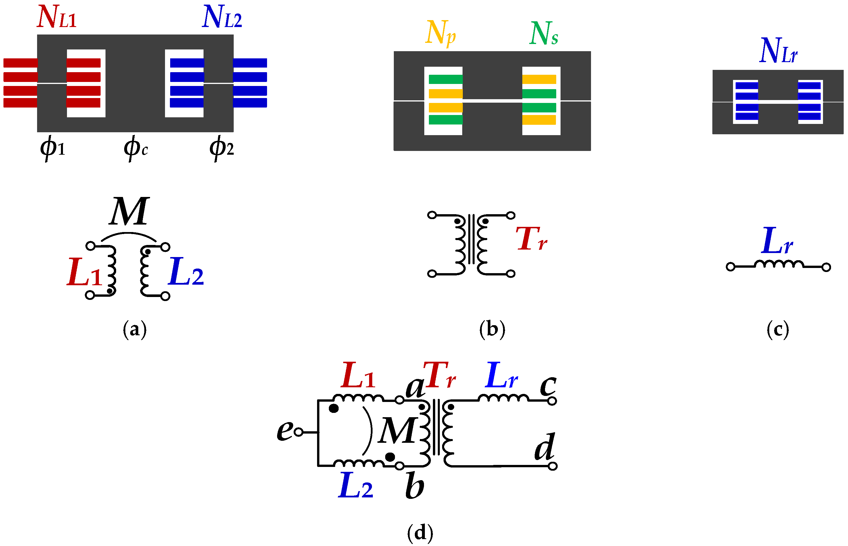
The traditional current-fed dual active bridge (CF-DAB) DC–DC converter includes multiple magnetic components, such as two DC inductors, a high-frequency transformer, and the external leakage inductor, as shown in Figure 1. And their diagrams of individual magnetic components are shown in Figure 2.
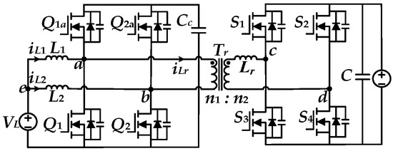
Figure 1.
Circuit diagram of CF-DAB converter [23].

Figure 2.
The individual magnetic components of traditional CF-DAB are shown in Figure 1 [23]. (a) Decoupled integration of two DC inductors. (b) High-frequency transformer. (c) External leakage inductor. (d) The magnetic components connection circuit.
Among them, Figure 2a shows the integration of two DC inductors, where NL1 and NL2 represent the number of windings corresponding to L1 and L2. Np and Ns represent the number of windings at the primary and secondary sides, and NLr represents the number of windings with the external series leakage inductor, which are shown in Figure 2b and Figure 2c, respectively. The magnetic components’ equivalent circuit of the traditional CF-DAB converter is shown in Figure 2d. With the traditional individual magnetic structure shown in Figure 2, the number of magnetic components is still large, and the power density cannot meet the requirements.
In order to further realize the integration, consider integrating the high-frequency transformer with the coupled inductor. As shown in Figure 3a, the windings on the two outer columns integrate two DC inductors and a transformer, that is, NL1 = Np1 and NL2 = Np2. Np1 and Np2 are the turns of PCB winding at the primary side of the transformer, and Np1 = Np2. However, the leakage inductor, shown in Figure 3b, still required an external series inductor. To construct the leakage inductor when all magnetic components are to be integrated together, an air gap needs to be introduced on the middle column based on Figure 3a, as shown in Figure 3c. However, once the air gap is increased, the magnetic flux leakage and loss of the central column will increase, and the DC inductance and leakage inductance are difficult to control. At a certain inductance and core section area, the more windings there are, the larger the air gap will be. To solve this problem, we can reduce the number of PCB layers to achieve a reduction in air gap, thereby reducing the losses and the cost of PCB. Then, to reduce the number of PCB layers, two side columns on the basis of Figure 3c are added. And the primary and secondary windings are separately connected to the two adjacent side columns on both sides of the magnetic core, which is shown in Figure 3d.

Figure 3.
The proposed DCI structure derivation process [23]. (a) Magnetic integration of two DC inductors and the transformer. (b) External series leakage inductor. (c) Three-column structure to integrate the leakage inductor. (d) Five magnetic columns structure to integrate the leakage inductor and reduce the required PCB layers.
The magnetic integration shown in Figure 3d is relatively complex. In order to simplify the structure, the flux of the magnetic core can be designed as
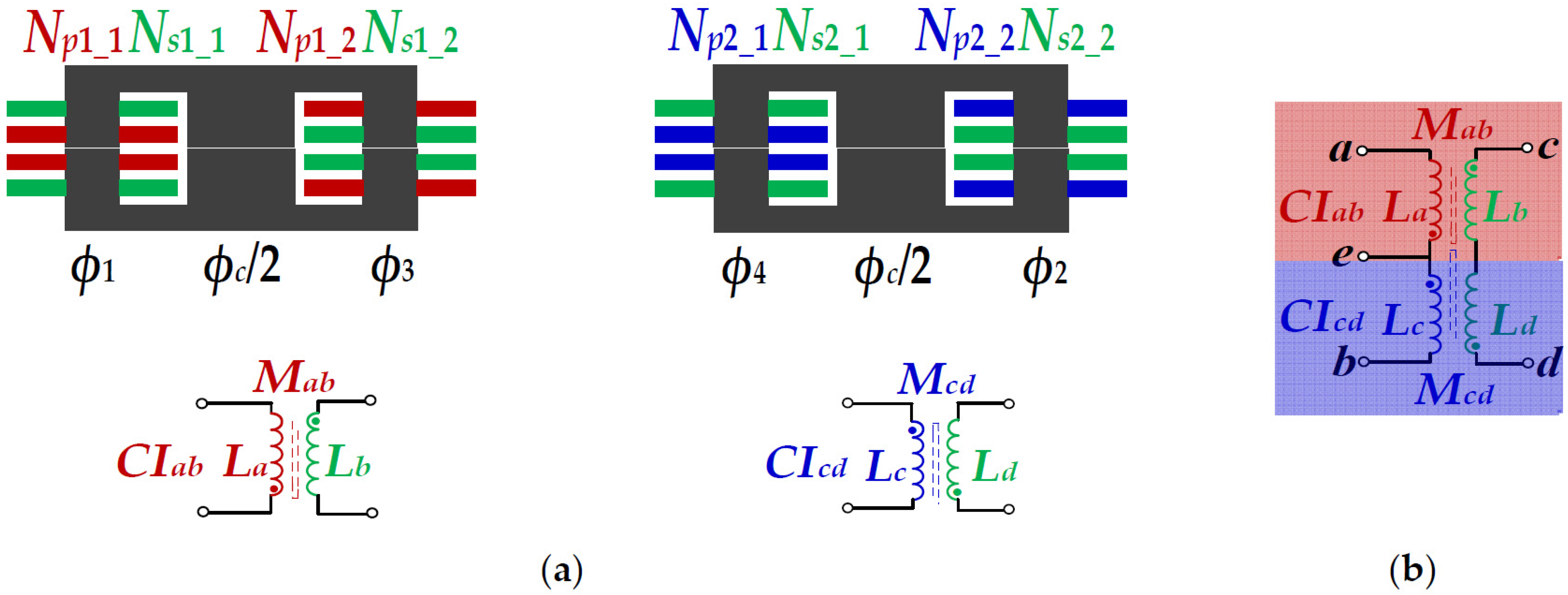
Then, the magnetic columns in Figure 3d can be separated, as shown in Figure 4a. And a magnetic integrated structure consisting of two EE cores can be obtained, which is called DCI structure in this paper. The circuit model of the DCI structure is shown in Figure 4b. Comparing the above structures in terms of magnetic components, volume, and losses, as shown in Table 1, it can be found that the DCI structure not only reduces the number of magnetic components, increases power density, and reduces the total volume of magnetic components, but also reduces the loss of the center column. And compared with the integrated structure shown in Figure 3c, the DCI structure achieves controllable integration of leakage inductance and DC inductance. In addition, the PCB winding structure and two EE magnetic core designs adopted in this scheme have the advantages of easy implementation and large-scale production. And the DCI structure has good scalability and can be extended to other important topologies. In LLC resonant converters, this structure can achieve high integration of the resonant inductor, magnetizing inductor, and transformer, improving power density. In isolated bidirectional converters such as isolated bidirectional buck-boost, this scheme can effectively integrate a transformer and DC inductor, and optimize soft switching characteristics by utilizing their controllable leakage inductance. This indicates that this study not only can optimize a specific converter but also can provide a universal magnetic integration solution for developing the next generation of high-performance power conversion systems.

Figure 4.
Proposed DCI magnetic integration [23]. (a) Magnetic core structure. (b) Circuit of the DCI.

Table 1.
Structural comparison.
In addition, in this structure, symmetrical design is adopted, that is, Np1 = Np1-1 + Np1-2, Np2 = Np2-1 + Np2-2, Ns1 = Ns1-1 + Ns1-2, and Ns2 = Ns2-1 + Ns2-2.
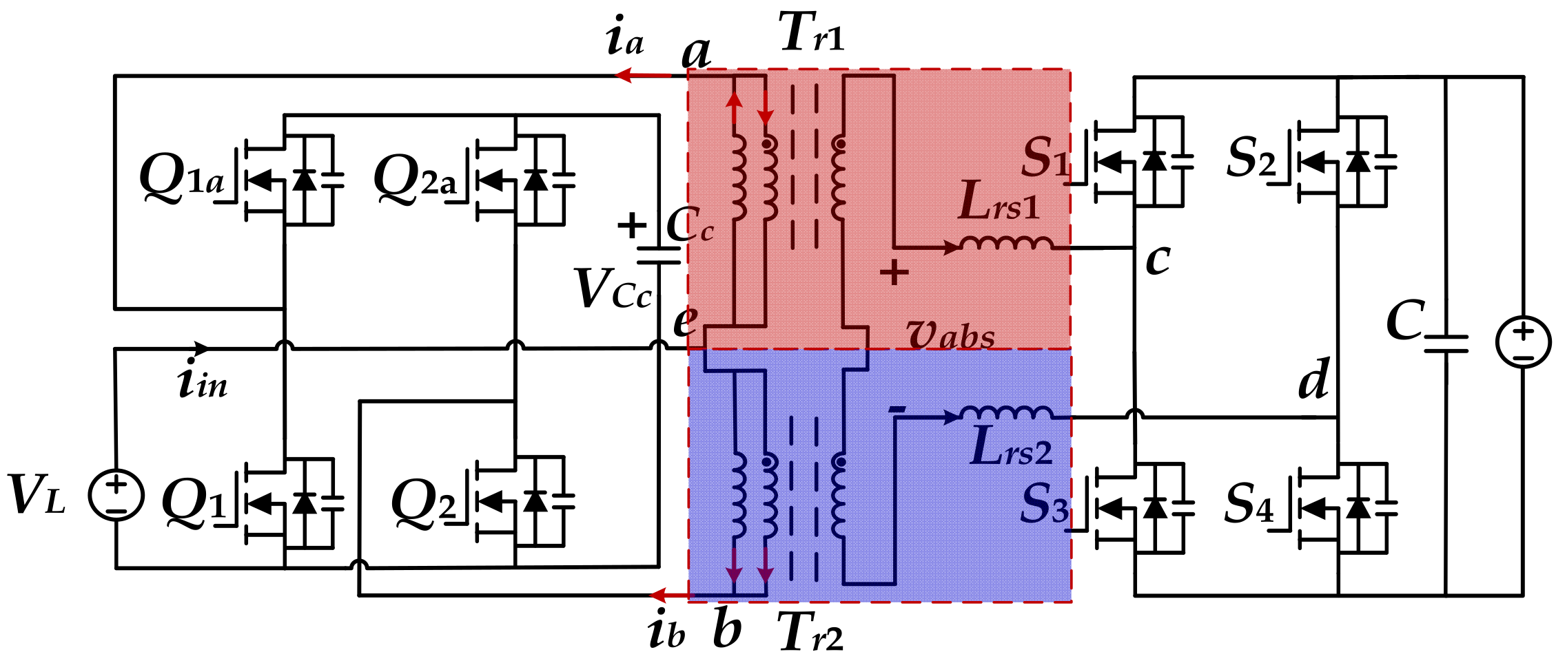
Based on the derived DCI, the topology structure of Figure 1 can be modified to the structure shown in Figure 5, where the red and blue parts represent the DCI structure. For the modified CF-DAB converter, VL represents the wide input voltage range on the low-voltage side, VH represents the output voltage, Tr1 and Tr2 are two identical transformers, ia represents the primary current of transformer Tr1, ib represents the secondary current of transformer Tr2, Lrs1 and Lrs2 represent the internal leakage inductor of the transformer, and L1 and L2 represent the magnetizing inductor of the transformer, whose current is equivalent to the DC current in Figure 1, and VCc represents the clamp voltage of capacitor Cc. In addition, the magnetizing inductor here is equivalent to the DC inductor in Figure 1.
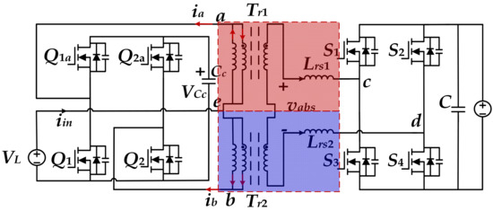
Figure 5.
Topology of CF-DAB Converter Based on DCI Structure [24].
2.2. The Principle of the Proposed Converter with DCI Structure
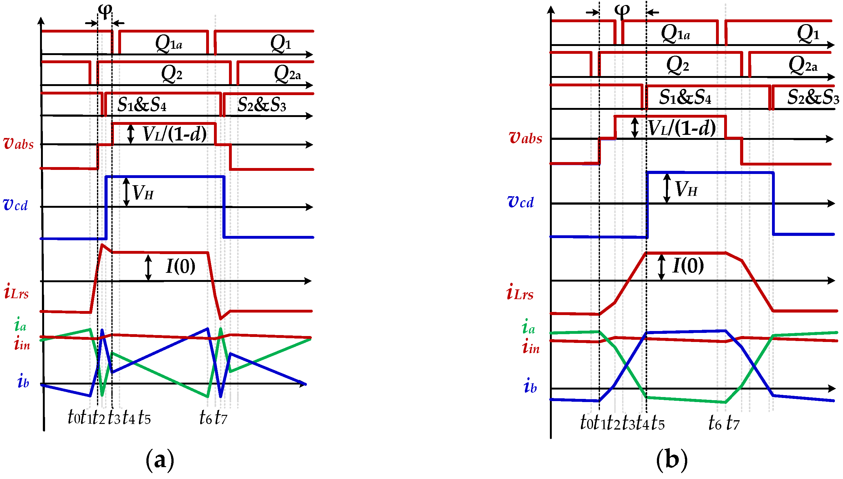
The waveform of this topology under PPS modulation is shown in Figure 6, where PWM is used to maintain the capacitor clamp voltage VCc, d represents the duty cycle of switches Q1 and Q2, and φ represents the phase difference between the rising edges of vabs and vcd. A change in the phase shift angle φ affects the magnitude of the leakage inductor current. According to the division interval of the phase shift angle, it can be divided into two working modes, Mode A(φ ∈ [0, (2d − 1)π]) and Mode B(φ ∈ [(2d − 1)π, π]). The corresponding waveform diagrams are shown in Figure 6a,b, respectively. In addition, the duty cycle of the secondary side switches signal is fixed at 50%, so the midpoint voltage waveform vcd of the secondary side bridge arm is a square wave with a duty cycle of 50%.
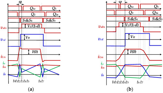
Figure 6.
Key waveforms [24]. (a) Mode A(φ ∈ [0, (2d − 1)π]). (b) Mode B(φ ∈ [(2d − 1)π, π]).
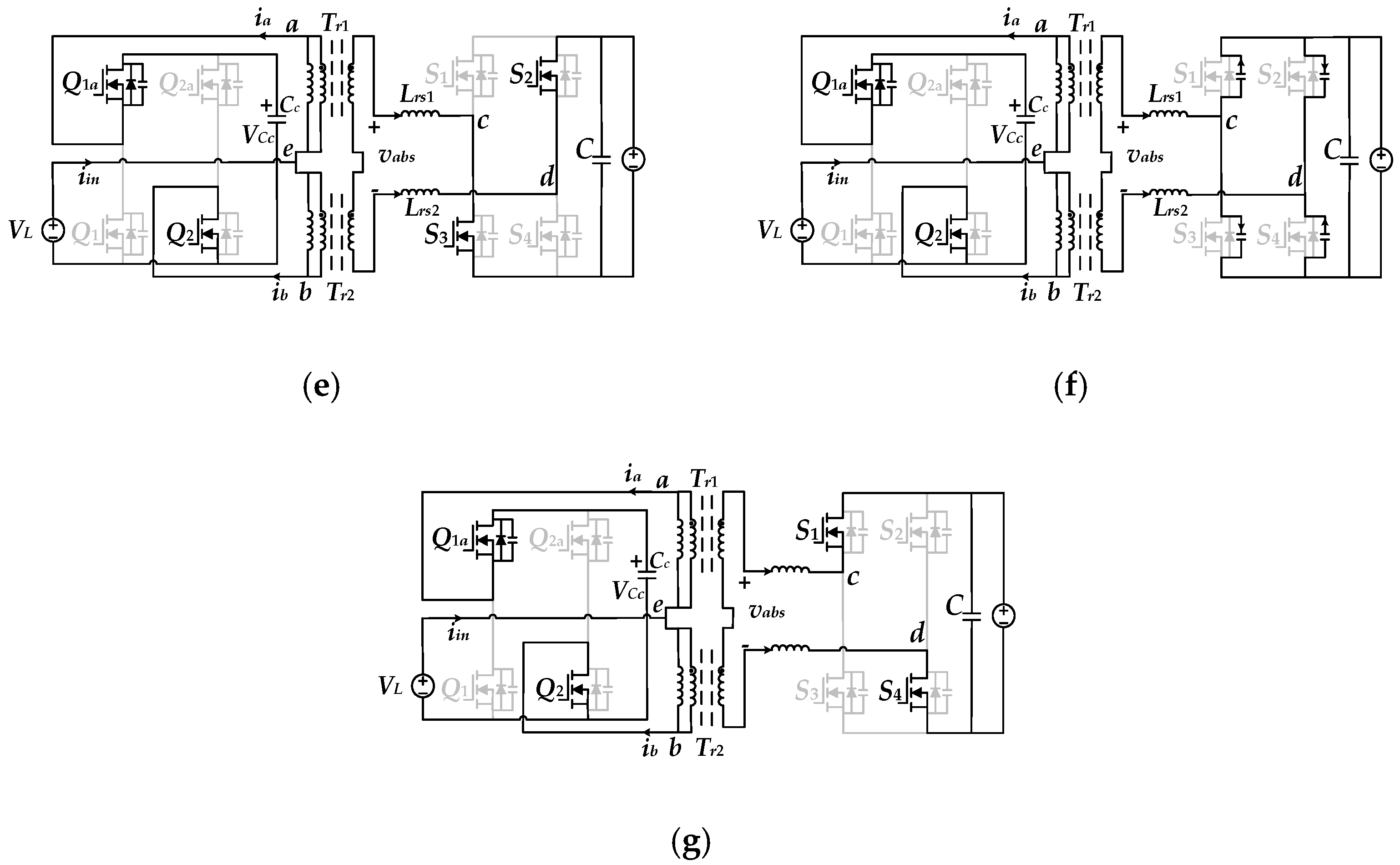
Since the working principles of Mode A and B are similar, in order to simplify the analysis, this article mainly focuses on Mode B. When the converter is working under Mode B, there are seven intervals within half a switching period, as shown in Figure 7. In addition, vae is defined as the voltage across the primary side of L1 and Tr1, and vbe is defined as the voltage across the primary side of L2 and Tr2.
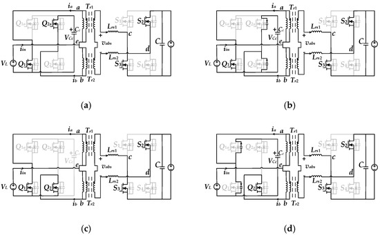

Figure 7.
Circuit working intervals in half cycle of the proposed DCI DAB converter [24]. (a) Interval I. (b) Interval II. (c) Interval III. (d) Interval IV. (e) Interval V. (f) Interval VI. (g) Interval VII.
Interval I: Before t0, the circuit modal diagram is shown in Figure 7a.
Interval II: t0–t1, the circuit modal diagram is shown in Figure 7b. At time t0, Q2a is turned off, while C2a is charged and C2 is discharged until Q2 conducts. Among them, the voltage at both ends of C2a and C2 satisfies (2), and the relationship between the current flowing through them is shown in (3).
From (2), it can be seen that when VCc remains constant, the changing trends of VCa2 and VC2 are opposite, with the same magnitude. Substituting into (3), the following expression can be obtained,
So, in order to achieve zero voltage turn-on of Q2, it is necessary to meet the following requirements: ib(t0) < 0.
Interval IV: t2–t3, the circuit modal diagram is shown in Figure 7d. At time t2, Q1 is turned off, while C1 is charged and C1a is discharged until Q1a conducts. Similarly to Interval II, it can be deduced that the condition for Q1a to implement soft switching is ia(t2) > 0.
Interval VI: t4–t5, the circuit modal diagram is shown in Figure 7f. At t4, S2 and S3 are turned off, while Cs2 and Cs3 charge, and Cs1 and Cs4 discharge until S1 and S2 conduct. It can be inferred that the condition for S1 and S2 to achieve ZVS is iLrs(t4) > 0.
Based on the above analysis, the conditions for integrating this circuit to achieve all switch ZVS are
Based on the calculation of instantaneous current, the current threshold for implementing Q1 and Q2 soft switching can be obtained, which can be referred to [3] and expressed as
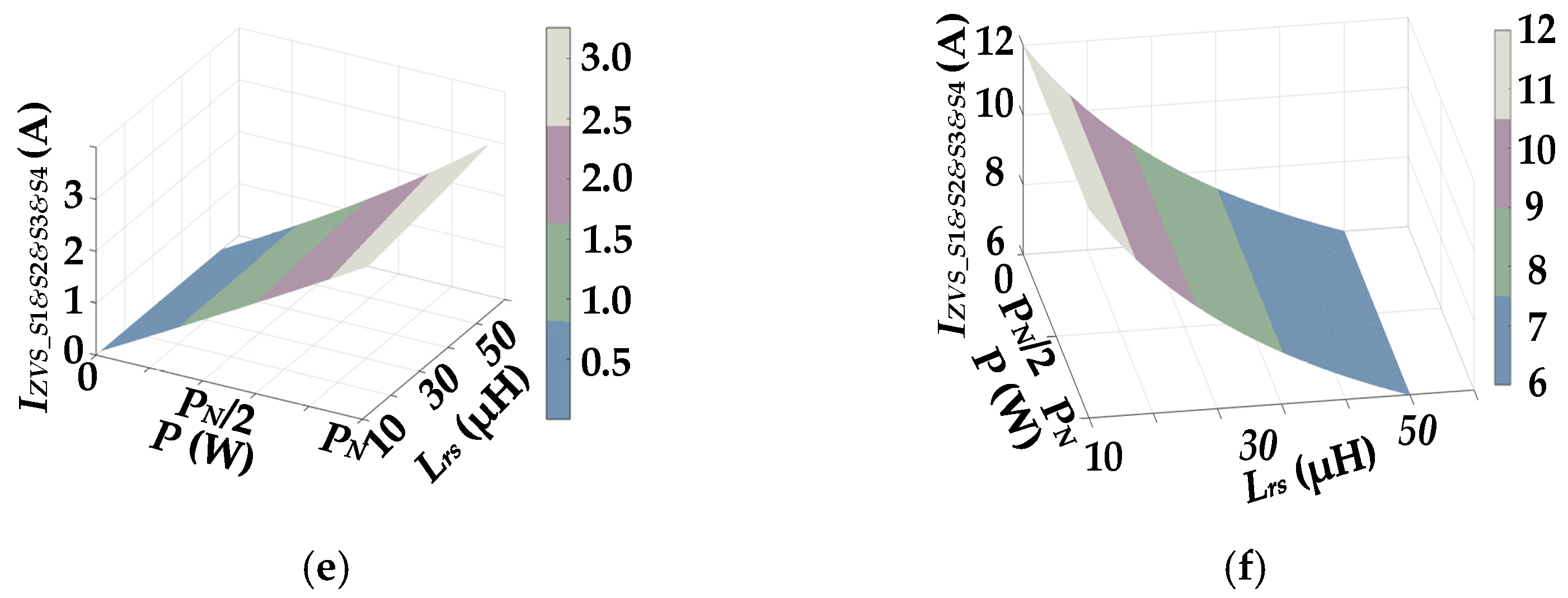
In addition, in order to visually display the ZVS range of all switches and the parameters that affect the ZVS range, this article takes VL = 18–36 V, VH = 300 V, f = 150 kHz, and PN = 1000 W as an example. According to (6), the ZVS range of Q1 and Q2 under different d and inductance can be obtained as shown in Figure 8a,b. It can be observed that whether d = 0.5 or d = 0.75, the current IZVS_Q1&Q2 are less than zero within the range of [2 μH, 10 μH], as shown in Figure 8a,b, which means that the low-voltage side switches can achieve full load range soft switching under different L1. Similarly, the ZVS ranges of Q1a and Q2a under different d and inductances are shown in Figure 8c,d, which can also achieve ZVS over the full load range under various inductances. The ZVS range of the high-voltage side switches S1, S2, S3, and S4 is shown in Figure 8e,f. It can be observed that ZVS cannot be achieved only when VL = 36 V and P = 0 W, but ZVS can be achieved under different leakage inductance in other load ranges. Additionally, it can be observed that the current threshold for implementing soft switching in low-voltage side switches increases as the leakage inductance decreases.
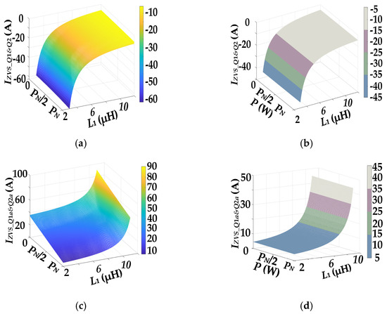
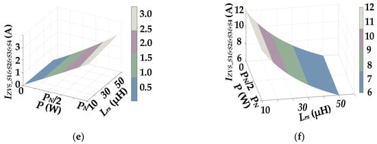
Figure 8.
ZVS range of switches [24]. (a) Q1 and Q2 when VL = 36 V. (b) Q1 and Q2 when VL = 18 V. (c) Q1a and Q2a when VL = 36 V. (d) Q1a and Q2a when VL = 18 V. (e) S1, S2, S3, and S4 when VL = 36 V. (f) S1, S2, S3, and S4 when VL = 18 V. (VL = 18–36 V, VH = 300 V, PN = 1 kW).
3. Design and Optimization of Planar Integrated DCI Structure
3.1. Design of Equal Air Gap Length
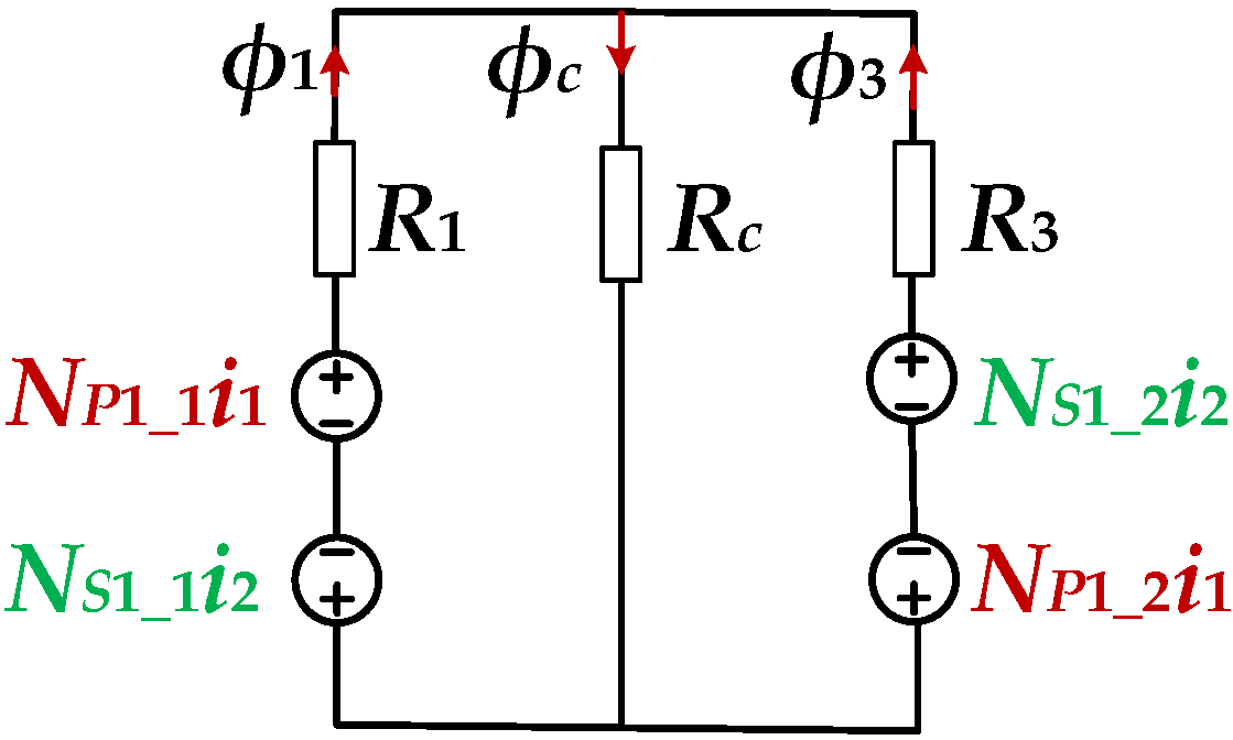
Because the two coupled inductors CIab and CIcd shown in Figure 4a are the same, to simplify the analysis, this article takes CIab as an example and creates its reluctance model as shown in Figure 9. Because the reluctance of the magnetic core is relatively small compared to that of the air gap, it can be ignored. Then, ϕ1 and ϕ3 can be obtained as
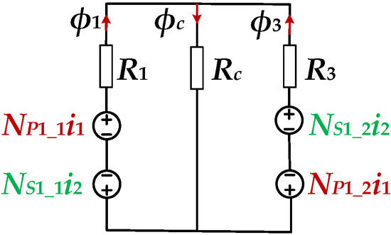
Figure 9.
The reluctance model of the coupled inductor CIab [23].
Therefore, according to Faraday’s law, the voltage at both ends of the transformer winding can be obtained as
The inductance matrix of the coupled inductor obtained by (7) and (8) is
The parameters of the transformer are
where Lm represents the equivalent magnetizing inductance, Lr_ab represents the leakage inductance, and Na:Nb represents the transformer turns ratio. From (9) and (10), it can be observed that CIab is related to the resistance and the number of windings. So, the coupled inductor can be designed based on the number of turns and gap size of the two magnetic cores.
For traditional EE core-based magnetic components, the cross-sectional area of the middle column is twice that of the outer column, and each winding is wound around the middle column. In the model designed in this article, the winding is wound on the outer column, which has a smaller cross-sectional area and leads to a higher magnetic flux density. Therefore, taking VL = 18–36 V, VH = 360 V, and PN = 1000 W as an example, this article proposes a design scheme with equal air gap for each column, which not only facilitates the design of a planar coupled inductor but also effectively reduces leakage of magnetic flux.
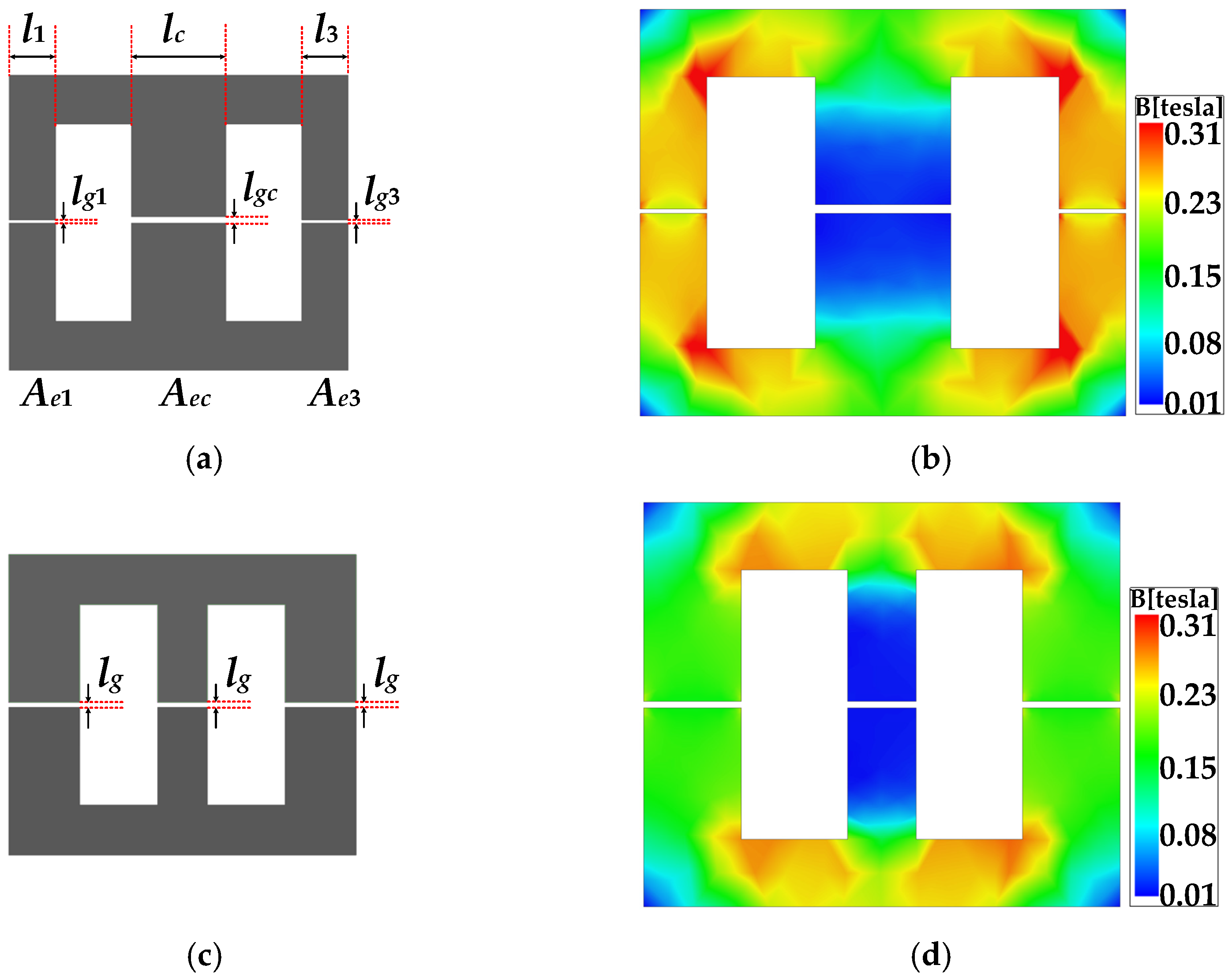
The coupled inductor structure based on the EE magnetic core is shown in Figure 10a. Based on this, an Ansys simulation model is established. In this model, the magnetic core material is DMR95, the B-H characteristic is defined according to the DMR95 datasheet, the boundary conditions are set as balloon boundaries to simulate an open field, the excitation current uses periodic current waveforms under full load, and the mesh type adopts a default control strategy based on the maximum element length. The magnetic simulation result is shown in Figure 10b. It can be observed that the outer column has a small cross-sectional area, high magnetic flux density, and high magnetic core loss.

Figure 10.
The optimization design of equal air gap length for each magnetic column and the Ansys simulation results. (a) Coupled inductor based on EE cores. (b) Magnetic flux distribution of EE cores. (c) Coupled inductor with the equal air gap length. (d) Magnetic flux distribution of equal air gap length design.
And the air gap and cross-sectional area can be expressed as
Combining R = l/μ0Ae, it can be concluded that the magnetic reluctance of two outer columns is equal, and it can be found that if the reluctance of the middle column and the outer column are not equal, the air gap of the two are also not equal.
Therefore, in order to reduce the magnetic flux density of the outer column, the cross-sectional area of the outer column can be increased, while in order not to change the overall volume of the magnetic core, the cross-sectional area of the middle column can be reduced. The relationship between air gap and cross-sectional area is as follows,
It can be observed that the air gap is directly proportional to the cross-sectional area. By combining Equations (13) and (14), it can be derived that if an equal air gap is designed, the resulting air gap length is
It can be observed that there must be a positive solution for lg, which proves the feasibility of equal air gap design. The coupled inductor structure diagram based on equal air gap design is shown in Figure 10c, and its magnetic simulation is shown in Figure 10d. The calculated cross-sectional area of the middle and outer columns under this design is
Comparing Figure 10b,d, it can be found that an equal air gap can reduce the magnetic flux density of the outer column. At the same time, the air gap in the middle column has decreased, and the leakage magnetic flux has also decreased accordingly. And the equal air gap design is also convenient for production practice, so the final choice is the equal air gap scheme.
In addition, the equal air gap scheme largely relies on geometric accuracy, and its small deviations can cause significant fluctuations in leakage inductance Lrs due to the inverse proportionality between inductance and air gap length. A small air gap can lead to excessive leakage inductance and increase magnetic core loss, while a large air gap can lead to a small inductance, which cannot effectively suppress ripple current and increase copper loss. Although the large air gap can reduce the magnetic flux density in the magnetic core and decrease core losses, the overall efficiency may decrease due to a significant increase in copper losses. Therefore, it is necessary to determine the specific air gap length based on the optimal efficiency point, and this design indeed requires a certain level of manufacturing precision to ensure its optimized performance.
3.2. Loss Optimization Design
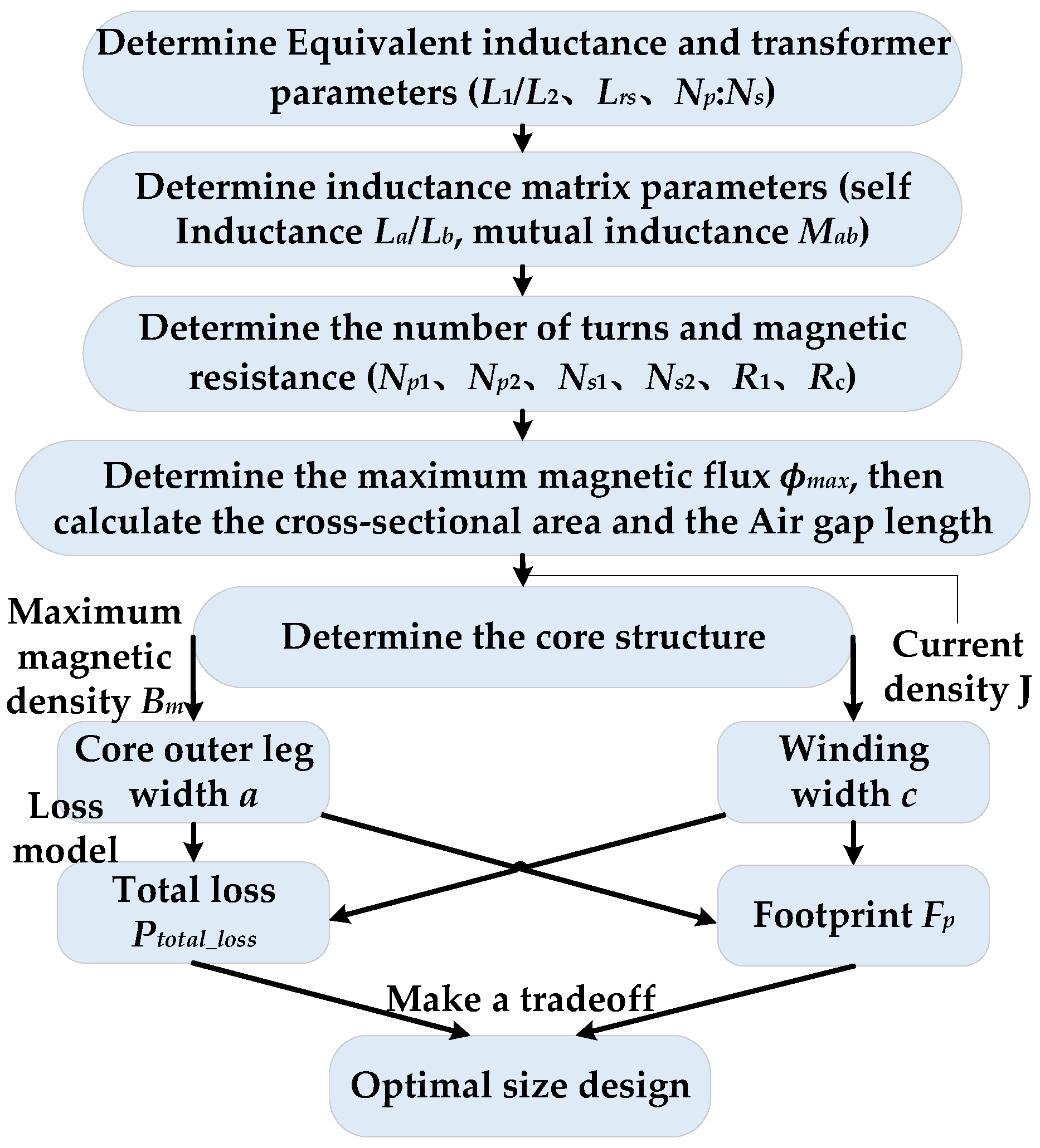
The parameter optimization design is carried out for the loss of DCI structure with equal air gap length under the above working conditions. The specific process is shown in Figure 11.
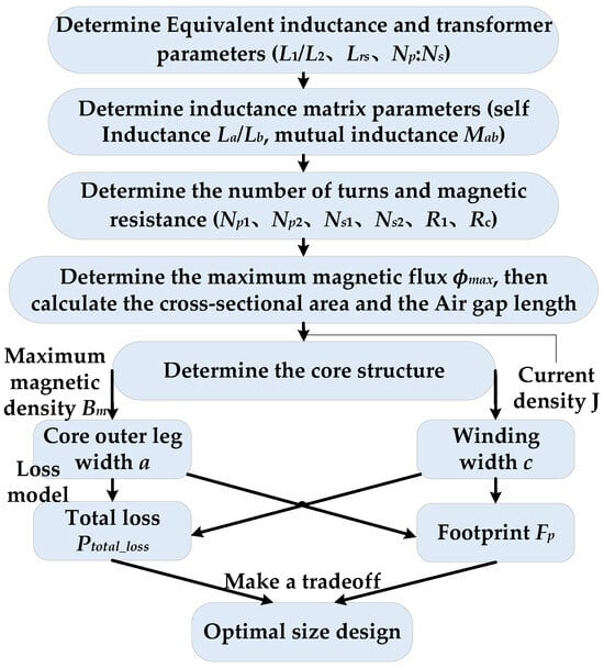
Figure 11.
Optimal design flowchart for the planar coupled inductor.
Combining the formula in Section 3, the parameter design process is shown as follows:
① Transformer turns ratio: under the control of voltage matching PPS, the designed transformer turns ratio is 1:5.
② Equivalent DC inductance: considering ZVS range, ripple current, and effective value of current, L1 and L2 are designed to be 6 μH.
③ Leakage inductance Lrs: considering the effective value of current, soft switching range, and maximum power capacity, the design of Lrs is 1.44 μH.
④ Inductance matrix parameters of coupled inductor: substitute L1, L2 and Lrs into (10) to obtain self-inductance La = 6 μH, Lb = 158 μH, and mutual inductance Mab = 30 μH.
⑤ Coupled inductor turns and reluctance: substitute the inductance matrix parameters into (9), and derive Np1 = 3, Np2 = 2, Ns1 = 11, Ns2 = 15, R1 = R3 = (2.04 × 10⁶) 1/H, and Rc = (2.92 × 10⁶) 1/H.
⑥ Cross-sectional area: the maximum magnetic flux of each column is obtained from (7), and finally the cross-sectional area and air gap length are derived. Where, the cross-sectional area is obtained as follows,
The recommended magnetic flux density is determined according to the working frequency of the converter.
⑦ Air gap: determine the length of the equal air gap according to (15).
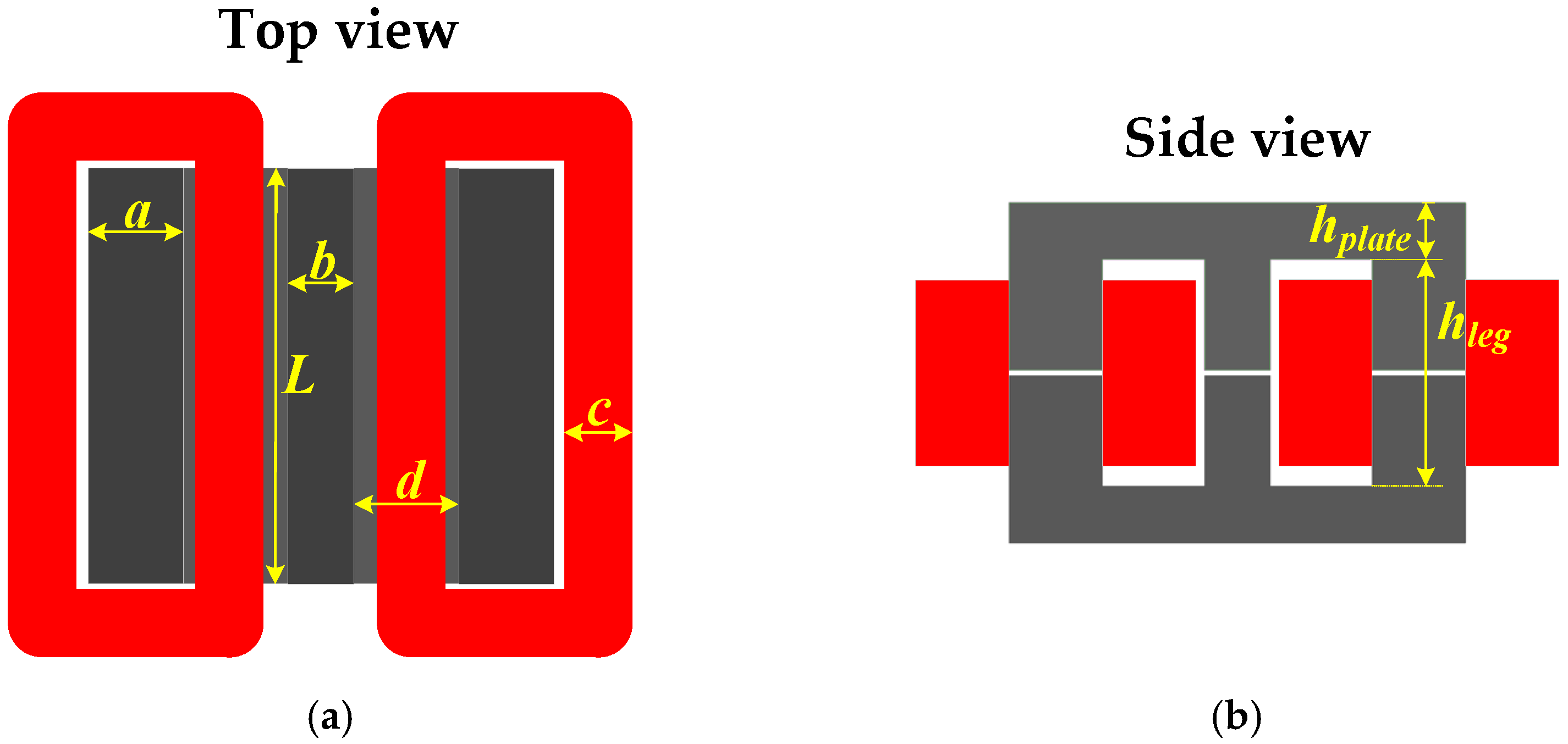
Finally, the optimized planar coupled inductor structure can be determined based on ⑤⑥⑦, as shown in Figure 12.

Figure 12.
Optimal planar coupled inductor structure. (a) Top view. (b) Side view.
It can be observed that in order to determine the size, it is necessary to determine the outer column width a and winding width c, where a = Ael/L, b = Aec/L, and hplate = Ael/l. The height of the magnetic core is determined by the thickness of the PCB board, and the area occupied by this planar coupled inductor is expressed by the following equation,
According to the square waveform modified Steinmetz formula, the iron core loss is expressed as
Among them, D is the duty cycle of the switch, Ve is the volume of the iron core, and γ, k, α and β are the Steinmetz parameters.
It is also known that the DC resistance of each winding is expressed as
Among them, l represents the length of each winding layer, h represents the thickness of the copper skin, and σ0 represents the conductivity of copper. According to the Dowell one-dimensional AC impedance model, the AC resistance can be calculated as
Among them, M is the number of winding layers, M’ is the real part of M, D′ is the real part of D, and μ0 is the vacuum magnetic permeability. The winding loss can be obtained from (23).
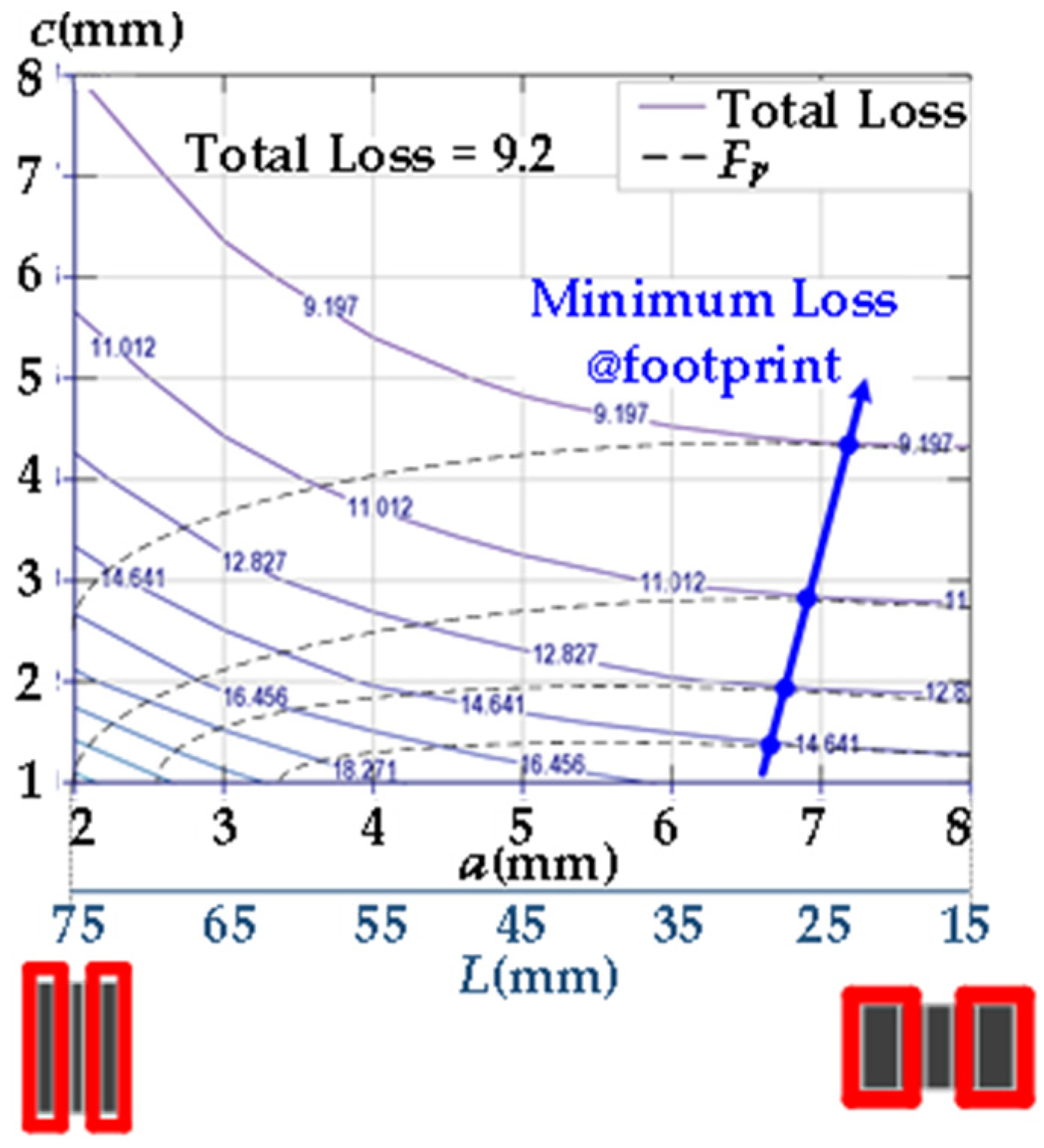
By combining (19) and (23), it can be found that both the core loss and winding loss can be expressed as functions of a and c. In this paper, Fp and the total loss of the planar multiwinding coupled inductor are taken as optimization objectives, so the relationship between total loss and Fp can be obtained, as shown in Figure 13, where the red box represents the winding.
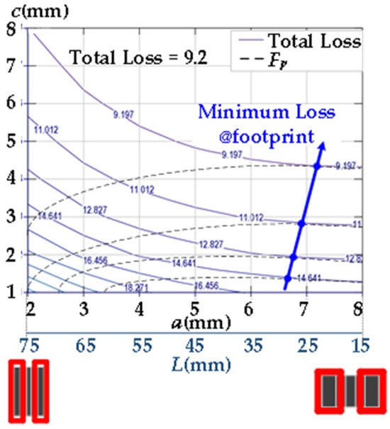
Figure 13.
Total power loss calculation with different a and c.
The solid line in the figure represents the waveform of total loss, the dashed line represents Fp at different values of a and c, and the blue tangent point represents the optimal design point, that is, the minimum loss point at a given Fp. It can be found that as Fp increases, the total loss decreases. However, the change in Fp required to reduce the same total loss will increase as the total loss decreases, that is, the degree of decrease in total loss will weaken as Fp continues to increase. Therefore, the final optimization solution is a compromise between Fp and total loss. Based on this, the optimization interval of Fp can be obtained, and the final optimization design point can be selected by combining Figure 13. The final parameter design is determined as a = 6.85 mm, L = 46.5 mm.
4. Experimental Verification
In order to verify the feasibility of the proposed DCI structure with equal air gap planar coupled inductors for the CF-DAB converter and its optimized design, an experimental prototype is designed based on the parameters listed below, as shown in Table 2. And according to the voltage, current stresses and margin that should be considered, device type IPP023N10N5 from Infineon company is selected for the low-voltage side switches, and device type UJ3C065030K3S from United-SiC company is selected for the high-voltage side switches. In addition, the dead time is set to 200 ns to achieve reliable zero voltage switching.

Table 2.
Experimental prototype parameters.
This prototype is a CF-DAB converter based on DCI structure with an input voltage range of 18–36 V, an output voltage of 360 V, and a power of 1 kW, as shown in Figure 14a. In addition, Figure 14b shows the dimensions of the designed magnetic core.
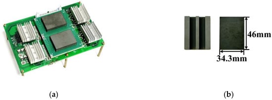
Figure 14.
The experimental prototype of the DCI CF-DAB converter. (a) Top view of complete converter. (b) Optimized core shape.
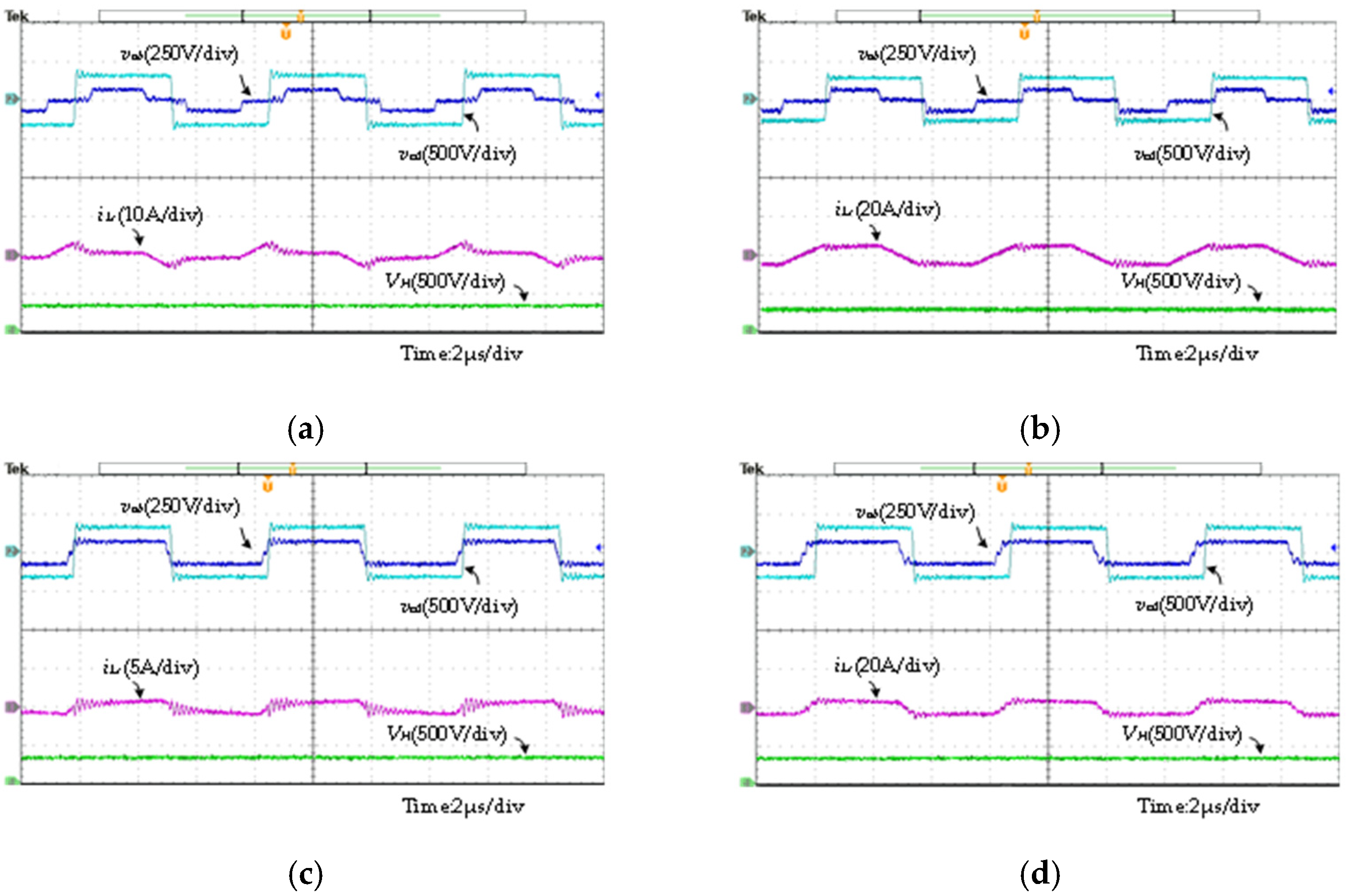
The steady-state waveforms of the proposed DCI CF-DAB under different loads are shown in Figure 15. Figure 15a,b are the waveforms under light load and full load with an input voltage of 18 V, respectively. Figure 15c,d are the waveforms under light load and full load with an input voltage of 36 V, respectively. It can be seen that the converter can achieve stable operation under this design.
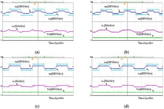
Figure 15.
Steady-state waveforms. (a) Light load when VL = 18 V. (b) Full load when VL = 18 V. (c) Light load when VL = 36 V. (d) Full load when VL = 36 V.
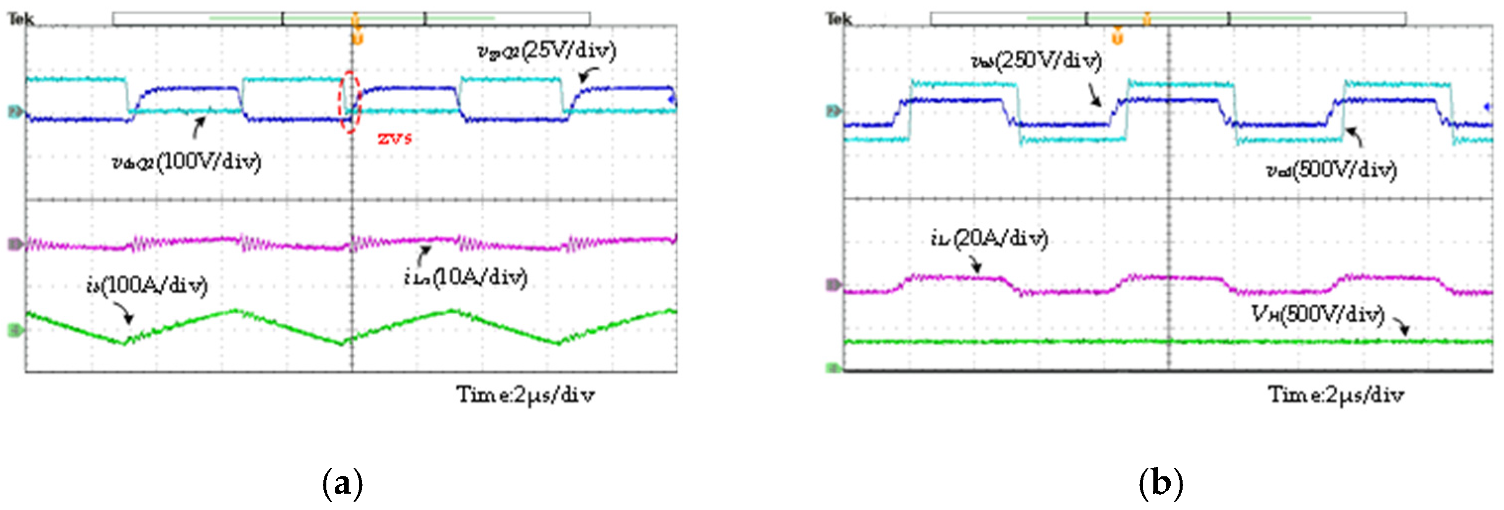
Figure 16a,b show the soft switching waveforms of Q2 and S1 in light load mode when the input voltage is 36 V. It can be seen that this design can achieve ZVS.
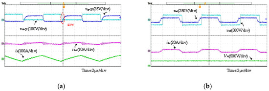
Figure 16.
Soft-switching waveforms for light load. (a) Q2 when VL = 36 V. (b) S1 when VL = 36 V.
Figure 17 shows the efficiency comparison before and after the equal air gap optimization design under different low-voltage side voltages and loads. It can be found that the optimized low-voltage side voltage of 36 V and load of 550 W has the highest efficiency, reaching 96.4%. It can also be observed that regardless of whether the low-voltage side voltage is 18 V or 36 V and load, the efficiency of traditional CF-DAB is always lower than that of converters using DCI structure. Moreover, after adopting the DCI structure, the efficiency of the optimized design with equal air gap is higher than that without optimization.
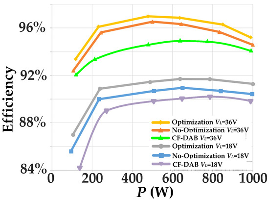
Figure 17.
Efficiency comparisons between optimization design, no-optimization design and CF-DAB at different voltages and different loads.
The power analyzer used in this paper has been calibrated for oversampling based on an external meter before measurement, with a voltage measurement accuracy of ±0.1% and a current measurement accuracy of ±1%. In addition, there is a 0.05–0.1% error in the power measurement process due to the length of the measurement probe and other reasons. Under the efficiency improvement shown in Figure 17, this error is acceptable, so the results presented are significant and reliable.
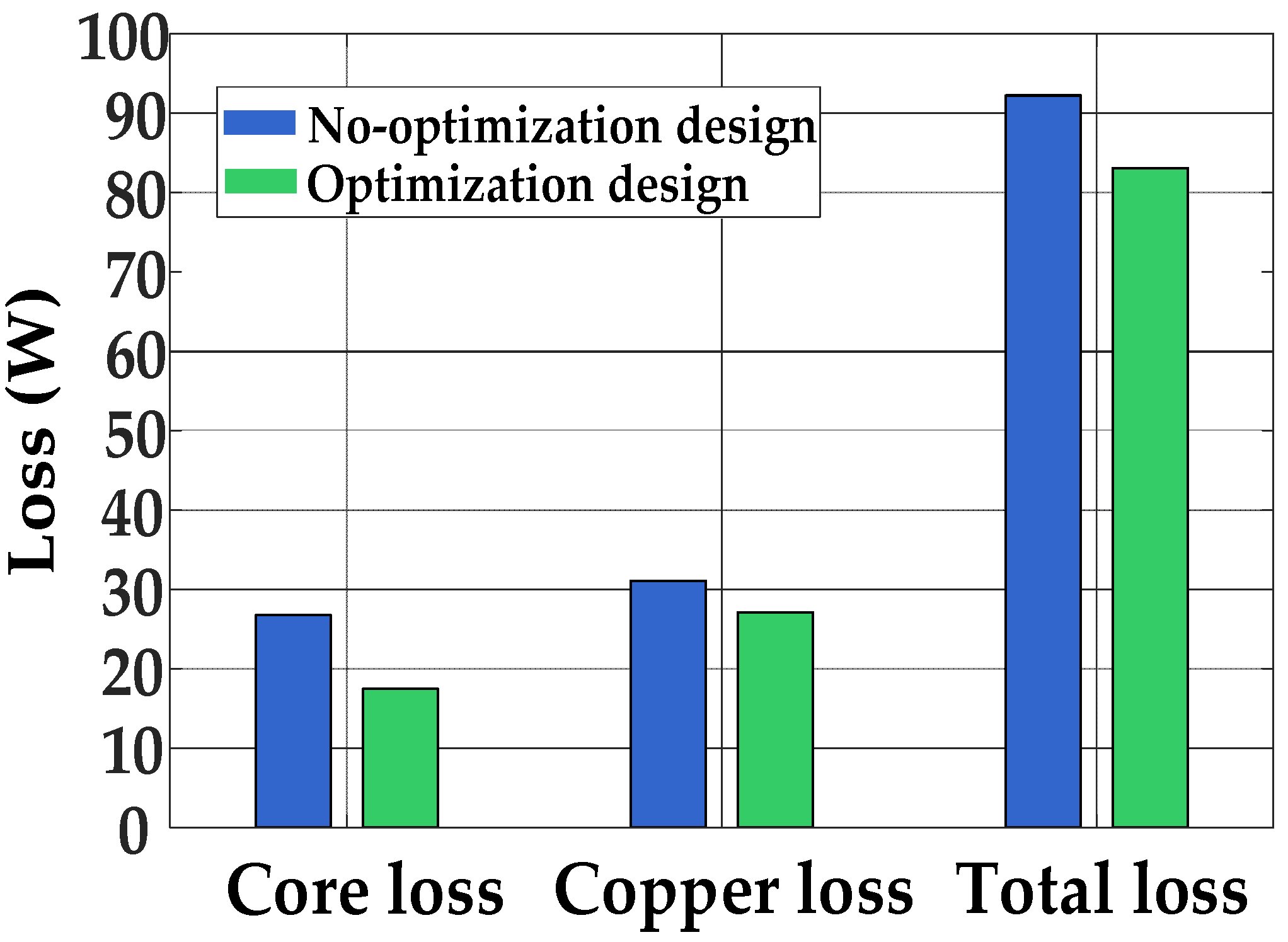
The comparison diagram of losses before and after optimization is shown in Figure 18. Based on this, a loss decomposition table as shown in Table 3 can be obtained. According to the data in Table 3, at VL = 18 V and rated power PN, the proposed optimization scheme has the lowest total loss, which is 9.1% lower than before optimization. This advantage mainly stems from the effective optimization of its magnetic core loss. The magnetic core loss of this optimization scheme is much lower than before optimization. Meanwhile, the optimized winding reduces copper loss, reflecting the rationality of its winding layout and the effectiveness of winding width. In summary, the equal air gap optimization scheme using the DCI structure is feasible and effective.
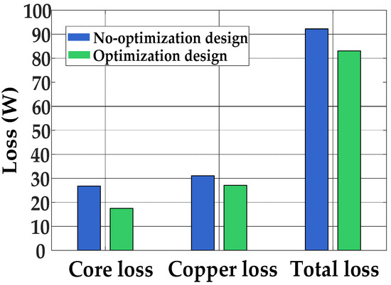
Figure 18.
Comparison chart of losses before and after optimization.

Table 3.
Loss decomposition table.
5. Conclusions
This article conducted a derivation of the DCI structure, integrating magnetic components to obtain a new CF-DAB topology. Based on the magnetic resistance model, an in-depth analysis was conducted on the inductance matrix parameters of the coupled inductor. The study found that the inductance matrix parameters are closely related to the key structural parameters, such as the number of winding turns and the length of the air gap. In response to the problems of uneven magnetic flux distribution and high losses caused by traditional air gap design, this article proposes an optimized design with equal air gap length, which effectively reduces the magnetic core density of the outer column, simplifies the production process, and provides a practical path for the industrial manufacturing of high-performance magnetic components. The geometric parameters of the planar coupled inductor are optimized, further improving efficiency and reducing losses. Finally, the proposed integration structure and optimization strategy are validated by building an experimental prototype. The experimental results show that the design scheme could improve overall efficiency, fully verifying its feasibility and effectiveness.
Author Contributions
Methodology, J.Z.; validation, Y.Z. (Yizhan Zhuang); investigation, Y.Z. (Yiming Zhang); resources, J.G.; writing—original draft, X.C. All authors have read and agreed to the published version of the manuscript.
Funding
This research was funded by National Natural Science Foundation of China under grant number 52407197.
Data Availability Statement
The original contributions presented in this study are included in the article. Further inquiries can be directed to the corresponding author.
Conflicts of Interest
The authors declare no conflicts of interest.
References
- Ilyushin, Y.V.; Novozhilov, I.M. Methodology of Inspection of Absolute Stability of Pulse Distributed Control System. In Proceedings of the 2019 XXII International Conference on Soft Computing and Measurements (SCM), St. Petersburg, Russia, 23–25 May 2019. [Google Scholar]
- China Society of Automotive Engineers. Technology Roadmap for Energy Saving and New Energy Vehicles; China Machine Press: Ningbo, China, 2020; pp. 97–104. [Google Scholar]
- Guo, J.; Han, H.; Xu, G.; Cai, Z.; Wang, H.; Sun, Y. Design considerations for PPS controlled current-fed DAB converter to achieve full load range ZVS and low inductor current stress. IEEE Trans. Ind. Appl. 2021, 57, 6261–6276. [Google Scholar] [CrossRef]
- Spiazzi, G.; Rossetto, L.; Mattavelli, P.; Gallo, E.; Cvejic, F. An Isolated Bidirectional Soft-Switching DC-DC Converter for Wide Input/Output Voltage Range. Energies 2024, 17, 6121. [Google Scholar] [CrossRef]
- Carvalho, E.L.; Meneghetti, L.H.; Carati, E.G.; Costa, J.P.D.; Stein, C.M.D.O.; Cardoso, R. Asymmetrical Pulse-Width Modulation Strategy for Current-Fed Dual Active Bridge Bidirectional Isolated Converter Applied to Energy Storage Systems. Energies 2020, 13, 3475. [Google Scholar] [CrossRef]
- Bathala, K.; Kishan, D.; Harischandrappa, N. Soft Switched Current Fed Dual Active Bridge Isolated Bidirectional Series Resonant DC-DC Converter for Energy Storage Applications. Energies 2023, 16, 258. [Google Scholar] [CrossRef]
- Meneghetti, L.H.; Carvalho, E.L.; Carati, E.G.; Denardin, G.W.; da Costa, J.P.; de Oliveira Stein, C.M.; Cardoso, R. Hybrid Inverter and Control Strategy for Enabling the PV Generation Dispatch Using Extra-Low-Voltage Batteries. Energies 2022, 15, 7539. [Google Scholar] [CrossRef]
- Gu, Q.; Xie, B.; Li, R.; Zhu, Z.; Zhang, Y. A ZVS Implementation Method of a Current-fed Dual Active Bridge Converter within the Full Load Range. In Proceedings of the 2024 IEEE Applied Power Electronics Conference and Exposition (APEC), Long Beach, CA, USA, 25–29 February 2024; pp. 2059–2062. [Google Scholar]
- Liu, J.; Zheng, Z.; Li, C.; Wang, K.; Li, Y. Automatic current sharing of input-parallel output-parallel dual active bridge converters with coupled inductors. In Proceedings of the IEEE 13th International Conference on Power Electronics and Drive Systems, Toulouse, France, 9–12 July 2019; pp. 1–6. [Google Scholar]
- Liu, J.; Li, C.; Zheng, Z.; Wang, K.; Li, Y. Current discrepancy mitigation of input-parallel output-parallel dual active bridge converters using cou- pled inductors. IEEE Trans. Ind. Electron. 2021, 68, 8182–8192. [Google Scholar] [CrossRef]
- Guo, Z.; Sha, D. Dual-active-bridge converter with parallel-connected full bridges in low-voltage side for ZVS by using auxiliary coupling inductor. IEEE Trans. Ind. Electron. 2019, 66, 6856–6866. [Google Scholar] [CrossRef]
- Liu, Y.; Xu, J.; Shuai, Z.; Li, Y.; Peng, Y.; Liang, C.; Cui, G.; Hu, S.; Zhang, M.; Xie, B. A Novel Harmonic Suppression Traction Transformer with Integrated Filtering Inductors for Railway Systems. Energies 2020, 13, 473. [Google Scholar] [CrossRef]
- Yang, J.-W.; Han, S.-K. A Si-FET-Based High Switching Frequency Three-Level LLC Resonant Converter. Energies 2019, 12, 3082. [Google Scholar] [CrossRef]
- Sha, D.; Wang, X.; Liu, K.; Chen, C. A current-fed dual-active-bridgedc–dc converter using extended duty cycle control and magnetic-integrated inductors with optimized voltage mismatching control. IEEE Trans. Power Electron. 2019, 34, 462–473. [Google Scholar] [CrossRef]
- Jiang, C.; Liu, H. A novel interleaved parallel bidirectional dual- active-bridge dc–dc converter with coupled inductor for more-electric aircraft. IEEE Trans. Ind. Electron. 2021, 68, 1759–1768. [Google Scholar] [CrossRef]
- Wang, Z.; Li, C.; Zheng, Z. A high-step-up low-ripple and high- efficiency DC-DC converter for fuel-cell vehicles. IEEE Trans. Power Electron. 2022, 37, 3555–3569. [Google Scholar] [CrossRef]
- Han, H.; Guo, J.; Xu, G.; Xu, J.; Liu, D.; Su, M. Three winding coupled inductor-based dual active bridge DC-DC converter with full load range ZVS under wide voltage range. IEEE Trans. Ind. Electron. 2022, 69, 6935–6947. [Google Scholar] [CrossRef]
- Zhang, Z.; Liu, C.; Wang, M.; Si, Y.; Liu, Y.; Lei, Q. High-efficiency high-power-density CLLC resonant converter with low-stray-capacitance and well-heat-dissipated planar transformer for EV on-board charger. IEEE Trans. Power Electron. 2020, 35, 10831–10851. [Google Scholar] [CrossRef]
- Kolahian, P.; Grimm, F.; Baghdadi, M. A Comprehensive Review on Planar Magnetics and the Structures to Reduce the Parasitic Elements and Improve Efficiency. Energies 2023, 16, 3254. [Google Scholar] [CrossRef]
- Zhang, J.; Ouyang, Z.; Duffy, M.C.; Andesen, M.A.; Hurley, W.G. Leakage inductance calculation for planar transformers with a mag- netic shunt. IEEE Trans. Ind. Appl. 2014, 50, 4107–4112. [Google Scholar] [CrossRef]
- Mu, M.; Xue, L.; Boroyevich, D.; Hughes, B.; Mattavelli, P. Design of integrated transformer and inductor for high frequency dual active bridge GaN charge for PHEV. In Proceedings of the IEEE Applied Power Electronics Conference and Exposition, Charlotte, NC, USA, 15–19 March 2015; pp. 579–585. [Google Scholar]
- Li, B.; Li, Q.; Lee, F.C. High-frequency PCB winding transformer with integrated inductors for a bi-directional resonant converter. IEEE Trans. Power Electron. 2019, 34, 6123–6135. [Google Scholar] [CrossRef]
- Guo, J.; Wang, H.; Xu, G.; Li, X.; Sun, Y.; Su, M. Dual Coupled Inductors with Controllable Integrated Leakage Inductance and CM Noise Suppression for CF-DAB Converter. IEEE Trans. Power Electron. 2023, 38, 8033–8038. [Google Scholar] [CrossRef]
- Guo, J.; Wang, H.; Xu, G.; Han, H.; Su, M. Dual-Transformer-Based DAB Converter with Controllable Integrated Inductances. IEEE Trans. Power Electron. 2024, 39, 6376–6390. [Google Scholar] [CrossRef]
Disclaimer/Publisher’s Note: The statements, opinions and data contained in all publications are solely those of the individual author(s) and contributor(s) and not of MDPI and/or the editor(s). MDPI and/or the editor(s) disclaim responsibility for any injury to people or property resulting from any ideas, methods, instructions or products referred to in the content. |
© 2025 by the authors. Licensee MDPI, Basel, Switzerland. This article is an open access article distributed under the terms and conditions of the Creative Commons Attribution (CC BY) license (https://creativecommons.org/licenses/by/4.0/).


