Article

Real-Time Reconfiguration of PV Arrays and Control Strategy Using Minimum Number of Sensors and Switches

School for Electrical and Mechanical Engineering, The University of Adelaide, Adelaide 5005, Australia
*
Author to whom correspondence should be addressed.
Energies 2025, 18(22), 5866; https://doi.org/10.3390/en18225866
Submission received: 5 September 2025 / Revised: 16 October 2025 / Accepted: 3 November 2025 / Published: 7 November 2025
(This article belongs to the Special Issue Intelligent Control for Electrical Power and Energy System)

Abstract

This paper presents a reconfigurable switching circuit and control methodology for mitigating power losses in photovoltaic (PV) systems under partial shading. The proposed hardware uses a simplified network of power MOSFETs and diodes to enable dynamic reconfiguration between series and parallel connections, improving energy yield with minimal conduction losses. Unlike conventional approaches that require irradiance measurements or extensive sensing, the control algorithm uses only per-module voltage and a single-current measurement to detect shading events in real time. A novel switching strategy reduces the number of actively controlled transistors, simplifying the control circuitry and reducing power dissipation. Both simulation and experimental results validate the method. Simulations of a 4-module PV system showed maximum power point (MPP) increases from 900 W to over 1100 W and from 460 W to 900 W, with full recovery to 1500 W after shading removal. Experimental verification on a 3-module setup under controlled shading yielded similar improvements: MPP increased from 38.4 W to 45.6 W and from 38.4 W to 45.8 W. These results demonstrate rapid adaptability, effective mismatch loss reduction, and maximisation of available power, making the proposed design a practical and low-overhead solution for commercial PV systems with non-uniform irradiance.

1. Introduction

Photovoltaic (PV) systems have been widely utilised to generate electricity, which commonly consist of long strings of series-connected solar modules, as shown in Figure 1a, which reduces the module output current and minimises power losses in cables and power converters. In addition, series-connected solar PV modules are connected to a central DC–DC converter to achieve maximum power at a given solar irradiance. However, in a practical system, not all PV modules are illuminated uniformly all the time. This may be due to several factors, including cloud coverage, soiling, and shading from nearby structures or trees. The topography of the solar PV system’s location can also be a factor, with all of these conditions varying with the position of the sun. Furthermore, there are times when some of the PV modules in the system are exposed to partial shading, hence resulting in low power output. Also, when a PV module is partially shaded, some PV cells may work in reverse bias and even reach breakdown voltage, which would not only lead to hot-spot issues but also damage the shaded cells. Under such shaded conditions, the common practice is to add a bypass diode in parallel with each module. The application of bypass diodes is to bypass the PV modules within a string with shaded PV cells, allowing the illuminated PV modules to continue delivering power.
Despite this widely adopted approach, bypass diodes cannot recover the power loss associated with mismatch among modules and only prevent catastrophic damage. Consequently, the overall system power drops under non-uniform irradiance, due to the losses in the bypass diode and its uncontrolled nature. This has motivated this research into more adaptive and efficient methods to manage partial shading effects.
To address these shading-induced performance degradations, research has progressed along several major directions, including the optimisation of PV array interconnection topologies, the use of module-level power converters, and dynamic reconfiguration of module connections.
In terms of connection topologies, methods such as Sudoku and total-cross-tied (TCT) configurations have been proposed to redistribute current paths and mitigate mismatch losses. Among these, the TCT topology is the most common due to its simplicity and ability to improve power extraction without the need for active components. However, TCT wiring is fixed, which limits its adaptability to dynamic shading conditions. Module-level power converters have also been implemented either as full power converters, which process the entire module output, or as partial power converters, which process only a fraction of the power. Partial power converters offer a balance between performance improvement and reduced converter losses, yet they still add complexity, cost, and potential reliability concerns at each module. Reconfiguration-based PV arrays, which dynamically alter the electrical connections among modules, have also been proposed in both full reconfiguration [1,2] and series–parallel reconfiguration forms [3,4]. Compared with fixed topologies such as TCT, reconfiguration methods can dynamically alter the wiring to maximise power output under any shading pattern and, compared with module-level converters, they avoid distributed active electronics and associated reliability issues. Thus, PV module reconfiguration offers better adaptability and reliability in shading-prone environments.
PV array reconfiguration techniques can be broadly categorised into full reconfiguration and series–parallel reconfiguration. Full reconfiguration allows any PV module in the array to be connected in series or parallel with any other module, providing maximum flexibility to achieve the global optimum configuration under any irradiance pattern. However, this approach requires a large number of switches, extensive control signal routing, and multiple voltage and current sensors, which increases system complexity, conduction loss, and cost. In contrast, series–parallel reconfiguration restricts parallel connections to consecutive modules within the same string, while unshaded modules remain in series. While this reduces flexibility, it significantly lowers hardware overhead and enhances reliability, making it more suitable for practical commercial PV installations.
Several reconfigurable switch networks have been proposed to improve performance under partial shading. For example, refs. [1,2] introduces a fully configurable architecture capable of establishing arbitrary series–parallel connections among modules. While such designs can theoretically maximise power output, they require N 2 + 3 N 2 switches and extensive inter-module wiring, leading to impractical hardware complexity and cost.
Ameen et al. [5] proposed a more compact solution using N 1 double-pole double-throw (DPDT) relays, equivalent to 4 N 4 transistors. While this reduces the component count, it introduces rigid configuration constraints, as modules can only be paralleled in fixed even-numbered pairs (e.g., Modules 1–2, 3–4). Consequently, configurations such as parallel operation between Modules 2 and 3 are not possible. This limits the topology’s adaptability under diverse shading conditions.
In addition, the use of electromechanical relays results in slower switching, higher power consumption, and increased mechanical wear, further reducing suitability for dynamic reconfiguration in real-world PV arrays.
Several recent works focus on limiting switch counts while enabling adaptive reconfiguration. For instance, ref. [3] integrates a DC–DC converter to improve voltage control and shading resilience, while [4] employs a detection mechanism to initiate parallel connections under shading. However, ref. [4] lacks shading-removal detection, and reconfiguration deconstruction relies on timed disconnection, potentially delaying energy recovery.
Other techniques, such as [6], permit module isolation under faults but do not support dynamic topology reconfiguration, limiting shading adaptability. In contrast, this paper proposes a selective reconfiguration strategy that combines lower hardware complexity with enhanced adaptability and faster response.
This paper presents a simplified PV module reconfiguration architecture that retains the practical constraint of forming parallel connections only between consecutive modules, similar to [4], but significantly reduces circuit complexity. By replacing two-thirds of the active switches with passive diodes, the proposed design lowers conduction loss and reduces the number of required control signals from 3 N 3 to N. Additionally, only one voltage measurement per module and a single overall current measurement are required, eliminating the need for distributed sensing or irradiance monitoring, as summarised in Table 1.
A key advancement of the proposed method lies in its control scheme, which enables real-time reconfiguration in response to both the onset and removal of shading conditions, thereby maximising energy harvesting. Unlike prior work [4], which relies on timing-based deconstruction, the presented approach enhances system responsiveness and reliability. These improvements make the system well suited for residential and commercial PV applications where adaptive reconfiguration under partial shading is critical.
The remainder of this paper is organised as follows. Section 2 introduces the proposed switching circuit topology, including voltage stress analysis and connection principles. Section 3 presents the real-time control algorithm for series–parallel reconfiguration, including flowcharts and implementation logic. Section 4 provides simulation studies demonstrating the reconfiguration method under different irradiance conditions. Section 5 presents the experimental setup and results, validating the method using a hardware prototype and solar simulator. Finally, Section 6 concludes the paper and discusses practical limitations.

2. Switching Circuit Topology

The proposed reconfigurable PV system consists of two types of blocks, as shown in Figure 1c, the beginning block on the right and the subsequent block on the left. The subsequent block has two diodes, which function like a bypass diode that allows the PV module in concern to be connected in parallel to the neighbouring PV module. When the series active switch, M ( k 1 ) , in the subsequent block is turned off, the series connection of the PV module, S ( k ) , that is connected by the switch will be changed to parallel with the previous PV module, S ( k ) . Notices that k is any integer between 1 and N, which is the number of PV modules in the PV system. The beginning PV module, S 1 , has an active bypass switch, Q 1 , constructed by connecting two MOSFETs back-to-back, and has no bypass diode. As a result, when Q 1 is on, S 1 can only be parallelly connected to S 2 or isolated from the network. Series connections between S 1 and S 2 are formed when Q 1 is off and the series active switch, M 1 is on. The PV module switch network can be constructed by the blocks shown in Figure 2, which consists of 2 N 3 diodes and N + 1 MOSFETs.
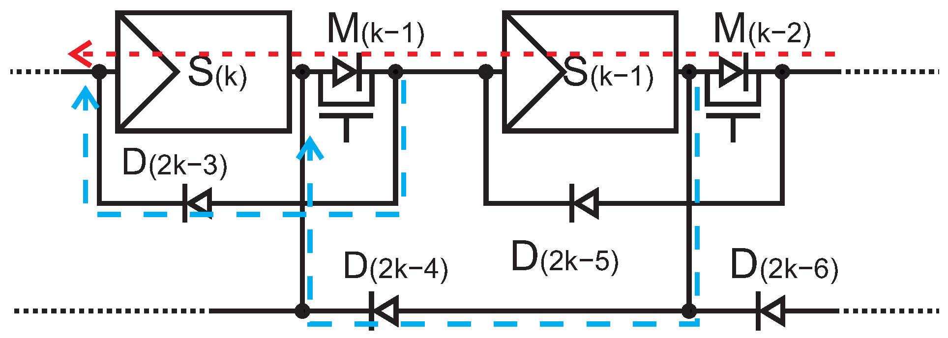
As an example, let us consider the connection between PV module S k and S ( k 1 ) . Normally, the MOSFET M ( k 1 ) and M ( k 2 ) are both turned on. When the PV module S ( k ) and S ( k 1 ) are both normally working, both diodes D ( 2 k 3 ) and D ( 2 k 4 ) will be inverted and can be regarded as disconnected switches. As a result, the PV module S ( k ) is connected in series to S ( k 1 ) and the current flows from S ( k 1 ) positive terminal thought M ( k 1 ) to S ( k ) negative terminal as shows in Figure 3 with the red arrow.
Figure 3 shows the current of a parallel connection. When MOSFET M ( k 1 ) turned off, the diodes D ( 2 k 3 ) and D ( 2 k 4 ) will be correctly biased and become conducting. Note that the two PV modules S k and S k 1 are connected in parallel, resulting in the currents directed through D ( 2 k 3 ) and D ( 2 k 4 ) as shown in the two blue arrow. These two PV modules are connected in series with the rest of the PV modules in the PV system.
On the other hand, for the connection of S 1 and S 2 , a series connection is formed by turning M 1 on and Q 1 off, and a parallel connection is formed by turning M 1 off and Q 1 on. It is worth mentioning that the voltage stress across each type of switch varies depending on its position and the switching configuration. The D ( k ) and Q 1 are only subjected to the voltage of a single module at most, as they connect adjacent modules in a parallel configuration. In contrast, the M ( k ) may experience higher voltage stress. The worst-case voltage stress occurs when the switch M ( N 1 ) , which is located at the terminal of the array, is turned off while the final module S ( N ) is disconnected. In this case, the switch blocks the total voltage of the preceding N 1 modules, resulting in a maximum stress of V ( N 1 ) , i.e., the voltage of N 1 V module . More generally, for switches M k 1 , the maximum voltage stress is V ( k 1 ) , which corresponds to the scenario where all modules from S N down to S k are either disconnected or configured in parallel, and the remaining modules from S ( k 1 ) to S 1 remain in series.
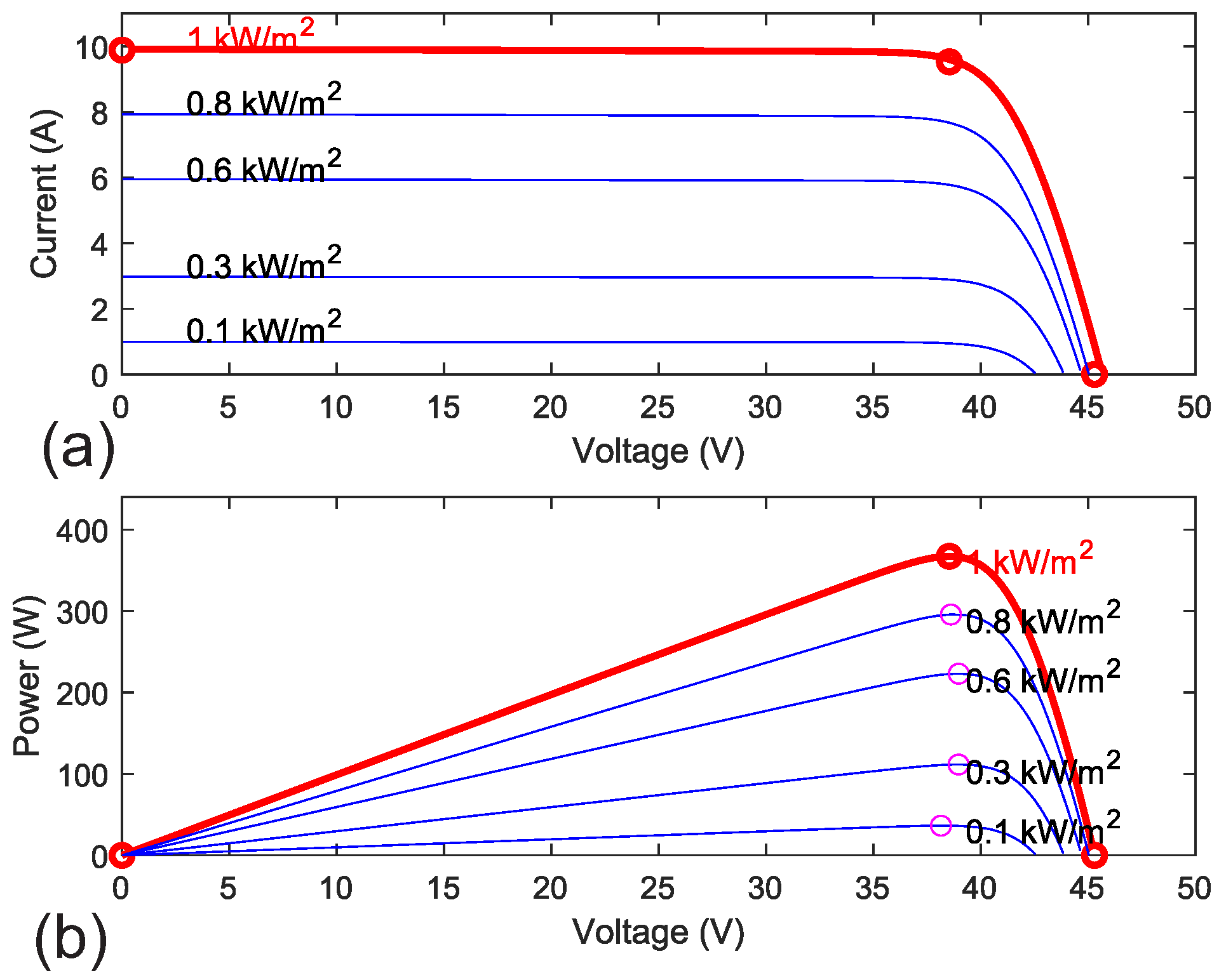
A typical current–voltage (I-V) and power–voltage (P-V) curve under different irradiance levels is shown in Figure 4. It is important to note that irradiance affects not only the short circuit current I S C but also the output voltage when operating at low current. In Figure 4a, assuming the modules are currently outputting 3 A, the module receiving 1000 W/m2 has the highest voltage at approximately 44 V, while the modules receiving 800, 600, and 300 W/m2 provide only 43.5 V, 43 V, and 41 V, respectively.
Furthermore, as each module operates closer to its I S C , the voltage drops even more significantly. This characteristic allows for an estimation of module performance based on module voltage when the system is operating at its global maximum power point (GMPP) and identifies the low-performance module by comparing the module voltage to the system’s average module voltage, V s Avg .

3. Control of Switching Network for Reconfiguration

When partial shading occurs during all PV modules connected in series, the shaded panel will be disconnected by the bypass diode in the switching network. Therefore, the shaded panel can be detected by detecting the voltage difference between the bypass diode instead of the direct measurement of the solar radiation intensity on each PV module.
The above system has provided a similar series-parallel reconfiguration as the full switch system in Figure 1b with a lower number of transistors and the possibility to use diodes with low conduction loss as switches in the network.
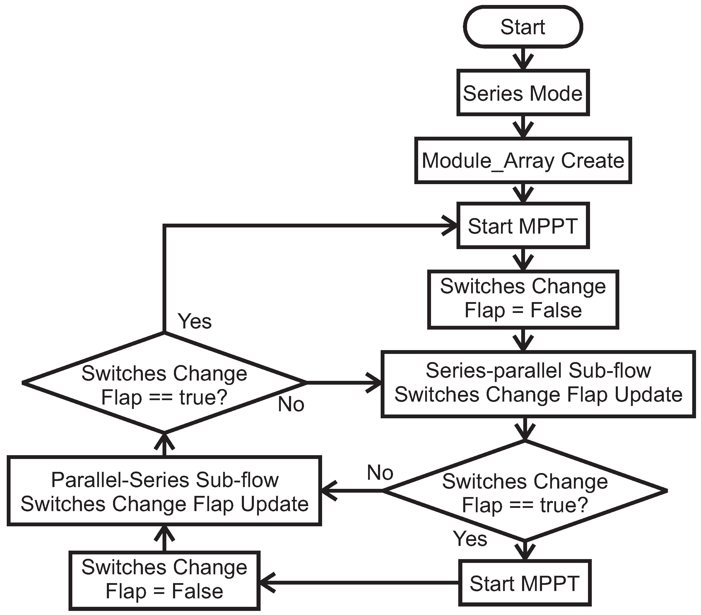
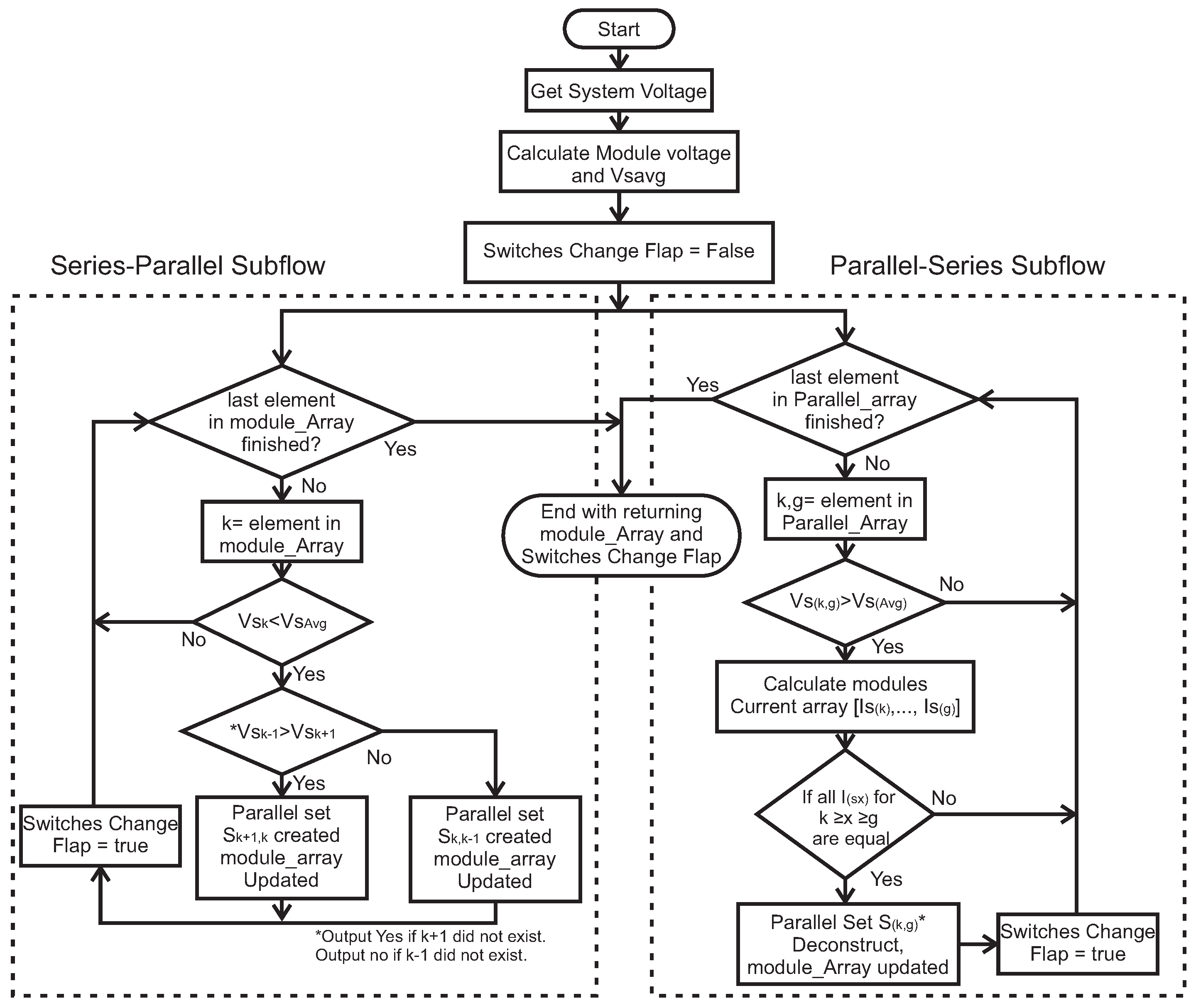
The control flow, as illustrated in Figure 5, operates as follows. Upon system startup, a series connection between all modules is initially established, the initial module array is created as [ 1 , 2 , 3 , , n ] and an initial MPPT operation is performed. Once the system finds the GMPP and starts to generate electricity, A series to parallel sub-flow, as shown on the left side of Figure 6, is performed. If the switches change flap is true, i.e., changes were made on the switch network, an MPPT will be performed before starting the parallel to series sub-flow as shown on the right side of Figure 6. After performing the parallel to series sub-flow, if the switches change flap is true, another MPPT will be performed before returning to the series to parallel decision flow and starting another cycle. It is worth mentioning that the switch network flap is reset to false at the beginning of each sub-flow.

3.1. Series-to-Parallel Reconfiguration

The series-to-parallel sub-flow is illustrated on the left side of Figure 6. The system voltage is measured and the voltage of each module is calculated using V s k = V k V k 1 or V s ( k , g ) = V k V g 1 , depends on whether it is a single module, S k , or a parallel set of modules, S k , g . The average module voltage, V s Avg , is then calculated as V s Avg = V N M o f f s e t , where M is the number of modules in series and an offset is introduced to prevent the parallel connections from forming when the PV system is operated with low performance difference across the module. Note that a parallel set could be interpreted as a module in series connections. The switch change flap is then reset to indicate no switch network changes were made.
Any module in module-Array with a voltage lower than V s Avg , denoted as S k , is then paralleled to its weaker neighbouring module. This effectively pairs a weak module with a relatively weaker neighbouring module, such as S k + 1 or S k 1 . This means either switch M k or M k 1 will be turned off, respectively. The module array is also updated form [ 1 ,   2 ,   3 , ,   k 1 ,   k ,   k + 1 , ,   n ] to [ 1 ,   2 ,   3 , ,   k 1 ,   [ k ,   k + 1 ] , ,   n ] for the case that S k + 1 is selected, and to [ 1 ,   2 ,   3 , ,   [ k 1 ,   k ] ,   k + 1 , ,   n ] for the case that S k 1 is selected. The [ k ,   k + 1 ] and [ k 1 ,   k ] means a parallel set of S k + 1 , k and S k , k 1 respectively.
It is worth mentioning that in case a parallel set, S k , g , is being evaluated. Either S k + 1 or S g 1 will be added to the parallel set, and either switch M k or M g 1 will be turned off. The module array is also updated form [ 1 ,   2 ,   3 , ,   g 1 ,   [ g ,   k ] ,   k + 1 , ,   n ] to [ 1 ,   2 ,   3 , ,   g 1 ,   [ k ,   k + 1 ] , ,   n ] for the case that S k + 1 is being added, and to [ 1 ,   2 ,   3 , ,   [ g 1 ,   k ] ,   k + 1 , ,   n ] for the case that S g 1 is being added.
When a parallel connection is formed, the switches change flap is changed to true, and after all modules in the module array that have a voltage lower than V s Avg have the parallel connections formed, the switches change flap will tell the main thread whether to perform another MPPT operation to go directly to the parallel to series sub-flow.
A 4-module reconfiguration system in Figure 7 is used to demonstrate the process of parallel connection forming and deforming, which will also be used to demonstrate the effectiveness of the proposed system. Note that in Figure 7, the voltage and current measuring point has been labelled along with all the components, including PV modules, S 1 , ,   S 4 , bypass diode, D 1 , ,   D 5 , series active switch, M 1 ,   M 2 ,   M 3 , and active bypass switch, Q 1 .
The operating condition of the 4-module system before reconfiguration is listed in the left column of Table 2, which is initially connected in series. Noted that the information of the PV module used in this example is the full panel listed in Table 3. A partial shading condition is being emulated in this setup. That is the modules 1 and 4 receive 1000 W/m2, while modules 2 and 3 receive 600 W/m2. The series connections are achieved by turning on switches M 3 , M 2 , and M 1 .
When the system operates at this configuration’s GMPP, i.e., 168.0 V, 5.48 A, the system voltages V 4 , V 3 , V 2 , and V 1 are recorded, and the individual module voltages are identified using equation V s k = V k V k 1 . Module S 1 and module S 4 exhibit voltages of 43.8 V, while modules S 2 and S 3 show voltages of 40.2 V, resulting in an average module voltage of V s Avg = 42 V.
Following the flowchart procedure in Figure 6, modules S 2 and S 3 in Figure 7, with voltages lower than 42 V, are identified for parallel reconfiguration. For module S 2 , since module S 3 has a lower module voltage than module S 1 , a parallel set S 3 , 2 is formed. Similarly, for module S 3 , a comparison of module voltages between modules S 2 and S 4 confirms that parallel set S 3 , 2 should be established. Consequently, the parallel set S 3 , 2 is formed by turning off M 2 , and a new MPPT operation is performed.

3.2. Parallel-to-Series Reconfiguration

The parallel to series sub-flow, as shown on the right side of Figure 6, is executed once the system stabilises with all the parallel connections in place, the voltage of the system is measured, and the module voltage and V s Avg is calculated again. It is worth mentioning that V s Avg is defined as V s Avg = V N M + o f f s e t , noted that a positive offset is in place to prevent a not strong enough parallel set being deconstructed.
All the parallel sets in the module array will be extracted and put into a parallel array for the following process. For any parallel set, S k , g , in the parallel array, the set voltage V s ( k , g ) is calculated by V s ( k , g ) = V k V g 1 as a module voltage and a check is performed to assess the energy-generating potential of each parallel set. Noted that g in S k , g is any integer number between 1 and k 1 , denoting the lower module in the parallel set, while k ranges from N to 2 and represents the upper module in the parallel set. This check involves comparing the parallel set voltage V s ( k , g ) with V s Avg . If V s ( k , g ) exceeds V s Avg , the parallel set is identified as operating in the high-voltage, low-current region, indicating that additional power may be extracted. At this stage, the current of each module within the parallel set is examined to verify current uniformity.
The current of the first module, I S k , in the parallel group is obtained by using the voltage drop across the diode D ( 2 k 4 ) , V S k 1 , and, subsequently, the current of each module in the parallel set can be found. To accurately sense both the module voltage (10–20 V) and the diode forward drop (10 mV to 1 V), a differential analog-to-digital converter (ADC) with an integrated programmable gain amplifier (PGA) can be employed. This configuration enables high-resolution measurements across a wide dynamic range, essential for reliable current estimation. Assuming the diode’s voltage-to-current function is defined as I = f ( V ) , the current of each module in the parallel set can be calculated as follows:
I S k = f ( V S k 1 ) , I S k 1 = f ( V S k 2 ) I S k , I S k 2 = f ( V S k 3 ) I S k I S k 1 , I S g + 1 = f ( V S g ) I S g + 2 I S g + 3 I S k 1 I S k , I S g = I sys f ( V S g ) .
An example parallel set from S k + 1 to S k 1 , denoted S ( k + 1 , k 1 ) , is shown in the middle section of Figure 2. The current of the first module, I S k + 1 , is determined by the voltage drop on diode D 2 k 2 , measured as V S k . The current of the second module, I S k , is then calculated as f ( V S k 1 ) I S k + 1 , and the current of the last module, I S k 1 , is given by I sys f ( V S k 1 ) . It is worth noting that the parallel set can be bypassed by D 2 k when the performance of the parallel set is still unable to match the other module in the system.
If the current across each module in the parallel set is found to be equal, or within range, and if the set has a higher voltage than V s Avg , it is concluded that all modules have recovered from shading conditions. In this case, the parallel set is dismantled, allowing individual modules to reconnect in series. This physically means that for parallel set s ( k , g ) , all the switch from M K 1 to M g is turned back on in order to form the series connections. The module array [ 1 ,   2 ,   3 , ,   [ g ,   k ] , ,   n ] will also be updated to [ 1 ,   2 ,   3 , ,   g , ,   k ,   ,   n ] to show a series connection between all module S g to S k is formed.
After the check has been performed in all parallel sets, if one or more reconfigurations have occurred, the switch’s change flap is changed to true, which tells the main thread to perform an MPPT operation before initiating a new cycle. If no reconfiguration is performed after the check, a new control cycle begins without performing MPPT.
While it is acknowledged that the forward voltage of a diode exhibits a strong dependence on junction temperature, this limitation is mitigated in the proposed system by placing all diode-connected transistors within a common heat sink. This configuration ensures a high degree of thermal coupling, thereby maintaining a relatively uniform temperature across all bypass diodes. Given that the objective is to identify relative mismatches in current among parallel modules—rather than to extract absolute current values—the uniform thermal environment allows for meaningful comparison. Specifically, the diode voltage of each module is compared against the average across all modules. Under the assumption of similar thermal conditions, deviations in forward voltage can be attributed primarily to differences in current, thus enabling the detection of shaded or underperforming modules.
The same 4-module system, as shown in Figure 7, in a series-parallel configuration, is used to demonstrate the action of parallel-to-series conversion. The operating condition of the system initially is listed in the right colume of Table 2, i.e., with modules S 2 and S 3 connected in parallel to form the parallel set S 3 , 2 , which is in series with modules S 1 and S 4 . In this setup, all modules receive 1000 W/m2. This configuration is achieved by turning on switches M 3 and M 1 , while M 2 is turned off. The switches that are turned on are highlighted in red in the figure.
When the system operates at the GMPP for this configuration, i.e., 126.15 V, 9.04 A, the system voltages V 4 , V 3 , V 2 , and V 1 are recorded, and the individual module voltages are identified as 41.06 V, 44.03 V, and 41.06 V for S 4 , S 3 , 2 , and S 1 , respectively. It is worth mentioning that the parallel set voltage is identified using V s ( k , g ) = V k V g 1 . The average module voltage is then calculated as V s Avg = 42.05 V. Next, the parallel set voltage is compared to V s Avg . In this case, since the voltage for set S 3 , 2 is higher than V s Avg , a current uniformity check is required.
To perform this check, the voltage across the parallel diode D 2 is measured and identified as −0.12 V. Using the diode characteristics, the current through S 3 is determined to be 4.52 A. By subtracting the current of S 3 from the system current of 9.04 A, the current through S 2 is also calculated to be 4.52 A, confirming current uniformity within this parallel set. Consequently, the parallel set is deconstructed, and a series connection is re-established by turning M 2 from off to on. Following the deconstruction of the parallel set, an MPPT operation is performed.

4. Simulation Study to Demonstrate Reconfiguration Method

An example of a 4-module reconfiguration system is shown in Figure 7. The PV module employed in the simulations and in the experiment is detailed in Table 3, where its key electrical specifications—including rated power, maximum voltage and current, and cell count—are summarised. The corresponding IV and PV characteristics for this module are depicted in Figure 4, providing the foundational performance curves upon which the dynamic reconfiguration analysis is based.
Simulation examples are provided for four distinct shading and reconfiguration scenarios. Each case is analysed in terms of switch states, module voltages, resulting current flow, and IV/PV characteristics.
The equivalent conduction resistances of the switching elements were derived directly from their datasheet specifications. The diode exhibits an initial forward voltage drop of 28 mV, and has an equivalent resistance of approximately 10 mOhm. In contrast, the switch presents an on-state resistance of 2.8 mOhm in its single-device configuration. For the back-to-back MOSFET arrangement employed in Q1, the combined resistance was taken as twice the single-device value, yielding 5.6 mOhm.
In the simulation environment, each switch element was thus modelled as a simple series resistor reflecting these equivalent resistances. This abstraction permits direct comparison of conduction losses between the ideal-diode controller and the MOSFET-based switch, while preserving computational efficiency and ensuring that dynamic reconfiguration effects can be observed without the complexity of full nonlinear semiconductor models.
The first example demonstrates the sensing and connections reconfiguration from series to parallel, which is controlled by the proposed control system on a four-module PV string under non-uniform irradiance. That is S 4 at 1000 W/m2, S 3 at 800 W/m2, S 2 at 500 W/m2, and S 1 at 300 W/m2. Figure 7 and the first column of condition 1 in Table 4 depicts the initial series connection of all four modules under differing shading levels. Switches M 1 through M 4 were enabled to establish a single-path current flow. The GMPP is at 169.4 V ( V 4 ) and 2.73 A (I), the module voltages were calculated as V S 4 = 44.70 V, V S 3 = 44.30 V, V S 2 = 43.26 V, and V S 1 = 37.14 V, yielding an average module voltage of V s Avg = 42.35 V.
Because V S 1 < V s Avg , the series-to-parallel decision flow in Figure 6 was invoked. Switch M 1 was opened to form the parallel set S 2 , 1 . The operating voltage of each PV module and system current after the reconfiguration have been shown in the second column of condition 1 at Table 4. The disables of M 1 isolate S 1 from the series chain, and Q 1 is enabled to connect it in parallel with S 2 . The individual branch currents are recombining at M 2 . As illustrated in Figure 8a, this configuration increases the extractable power from 463 W to 895 W, corresponding to 90.6% efficiency and a 193% improvement over the original series-only connection.
The second example demonstrated how the proposed control method handles a recovery of the same PV system from a partial shading condition. The irradiance on the four PV modules is uniform and is at 1000 W/m2. Consider the partial shading condition has just been removed and modules S 1 and S 2 are still connected in parallel, which switch M 1 is turned off and transistor Q 1 is enabled, resulting in the parallel set S 2 , 1 . Using the information listed in Condition 2 column 1 at Table 4, the average module voltage can be calculated and is V s Avg = 41.18 V. By applying V S 1 and the known on-resistance of Q 1 , the branch current of S 1 is calculated as 4.88 A. Given the total system current of 9.40 A, the complementary branch current of S 2 is determined to be 4.52 A. The minor discrepancy between these two values is attributed to the slight resistance difference between the ideal-diode path and the back-to-back MOSFET switch, which shifts the individual maximum power points (MPPs).
Because the parallel set voltage V S 2 , 1 exceeds V s Avg and the branch currents are closely matched, the deconstruction criterion of the parallel-to-series decision flow, as shown in Figure 6, is satisfied. In order to restore the series connection on all four modules, all switches M 1 M 4 are on and Q 1 is off, producing a unified current path through the series string.
Figure 8b shows the PV and IV curve on these conditions before and after the reconfigures. Before the reconfiguration, the global maximum extractable power under this configuration is 1161 W, corresponding to 77% efficiency. And after the reconfiguration, the new GMPP occurs at 1498 W, achieving 100% of the panel string’s summed individual MPPs and demonstrating full recovery of the original power capacity.

5. Experiential Result

The experiments were conducted using Karra 350 PV panel, which is listed in Table 3, from which one-third of the panel area was electrically isolated and treated as an individual “module” for testing purposes. The electrical characteristics of the full panel and individual “module” under standard test conditions (STC) are provided in Table 3. They are captured by Spire Sun Simulator 4600SLP.
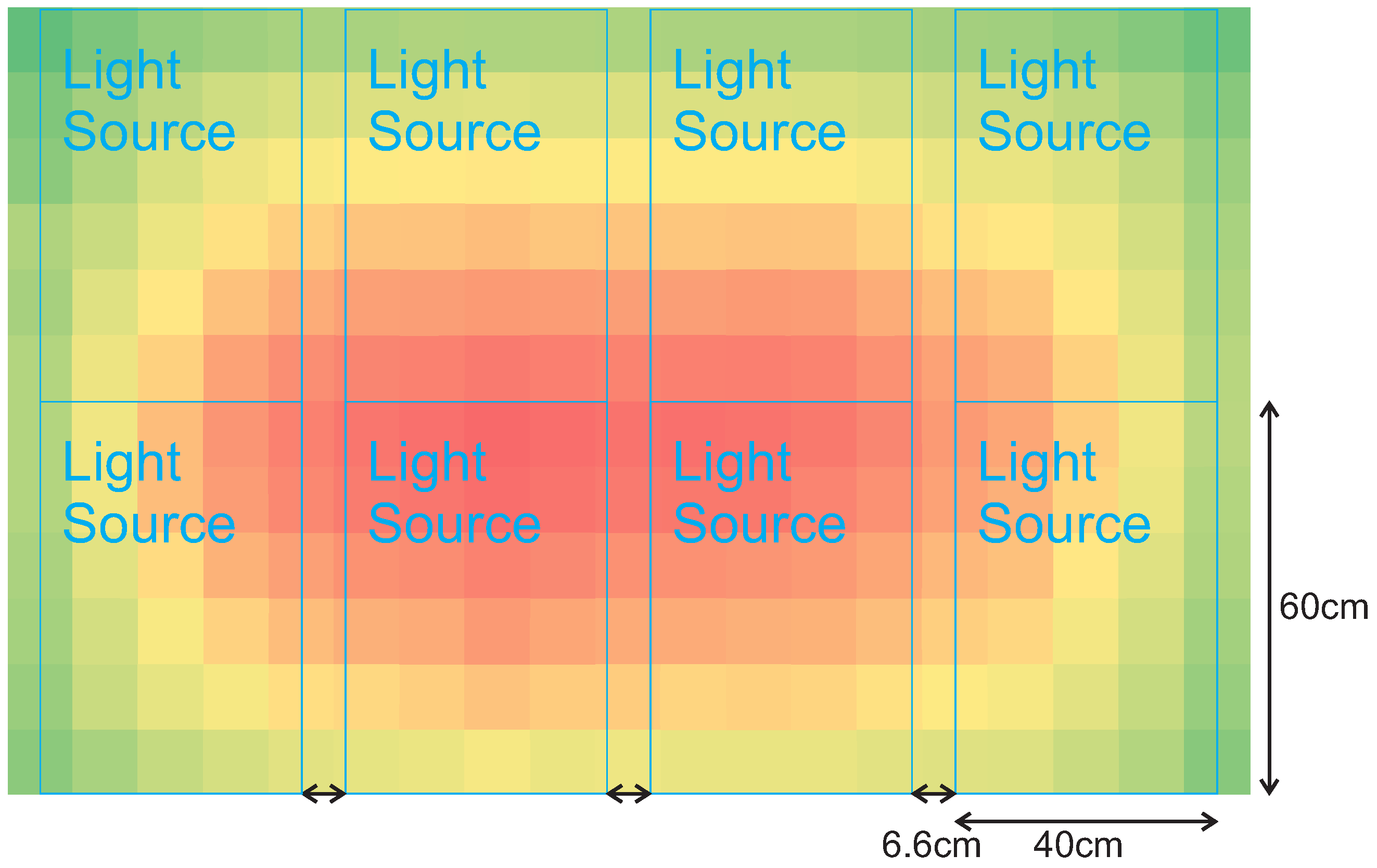
To evaluate the proposed reconfiguration method under controlled irradiance patterns, a custom solar simulator was constructed. The simulator consists of eight LED grow light panels arranged in a 4 × 2 grid, mounted above the PV panel plane. The vertical separation between the lights and the PV plane was fixed at 30 cm to ensure repeatable irradiance mapping. The resulting heat map is shown in Figure 9. The map shows higher irradiance in the central region, consistent with the overlapping beams from adjacent light panels.
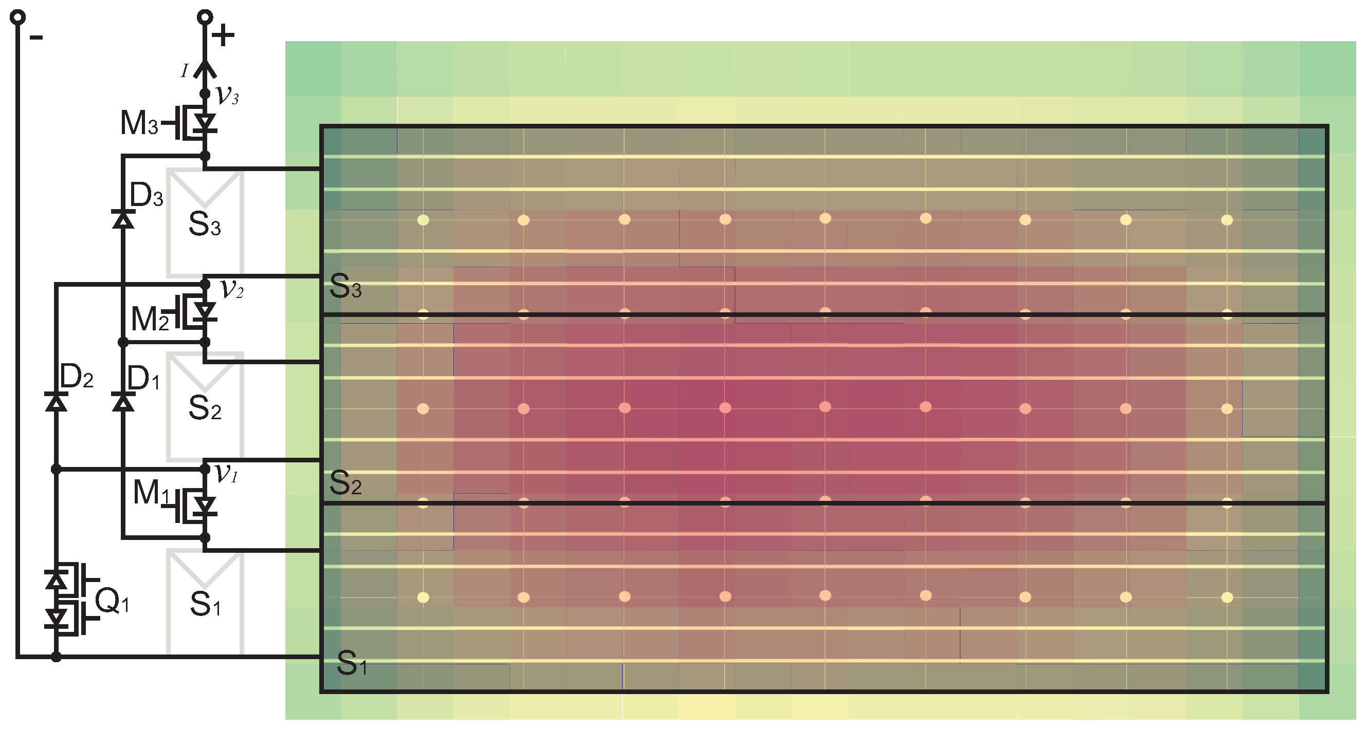
This irradiance profile was overlaid onto the PV panel geometry to determine the light incident on each submodule, as shown in Figure 10. In the configuration used for testing, the middle submodule S 2 received the highest irradiance, while the outer submodules S 1 and S 3 experienced similar, lower irradiance levels. These patterns were used to define the partial shading conditions in the test matrix.
A programmable DC electronic load (Tenma 72–13210, 300 W, 0–120 V, 0–30 A) was used to obtain IV characteristics for each test condition. This load are used as a data collection device as well. The internal voltage/current measurement resolutions of the load is 1/10 mV and 0.1/1 mA respectively, and typical accuracies of ± ( 0.03 % set + 0.025 % f . s . ) for voltage and ± ( 0.05 % set + 0.045 % f . s . ) for current. A control program communicated with the load to perform voltage sweeps from the open-circuit voltage V oc down to 0 V in fixed steps of 0.1 V. At each step, the load operated in constant-voltage mode, holding the target voltage for a dwell time of 1.5 s to allow current stabilisation before recording both voltage and current readings. The instantaneous power P = V I was calculated for each point, and the maximum power point ( P mpp ) was determined for each configuration.
Two experimental scenarios were evaluated to demonstrate the effectiveness of the proposed reconfiguration method. In both cases, the initial and reconfigured P-V and I-V characteristics are shown in Figure 11a,b, while the typical non-shaded P-V and I-V characteristics are illustrated in Figure 11c.
In the first test, partial shading was applied to submodules S 1 and S 2 (Figure 11a). With the active bypass switch disabled, the array current was limited by the lowest-performing module, S 1 , and no local maximum power point (LMPP) was observed. After reconfiguration, S 1 and S 2 were connected in parallel to form a combined unit S ( 2 , 1 ) , which was then placed in series with the fully illuminated S 3 . This increased the overall MPP from 38.4 W (three modules in series) to 45.6 W. Because S ( 2 , 1 ) produced higher voltage than S 3 under these conditions, S 3 was driven into reverse bias, activating its bypass diode D 3 and creating a LMPP near 12 V after reconfiguration.
In the second test, shading was applied to S 2 and S 3 (Figure 11b). Before reconfiguration, the bypass diode across S 3 automatically provided an alternative current path when S 3 entered reverse bias, resulting in the appearance of a LMPP. After reconfiguration, S 2 and S 3 were connected in parallel to form S ( 3 , 2 ) , which was then connected in series with the fully illuminated S 1 . This arrangement increased the MPP from 38.4 W (three modules in series) to 45.8 W, demonstrating improved utilisation of the available irradiance.
In both cases, the reconfiguration redistributed the mismatch losses more effectively, enabling a higher operating power point under the given shading conditions.

6. Conclusions

This work proposed a novel switching circuit and control methodology to address the reduction in output power of PV systems caused by partial shading. The design emphasises efficiency and simplicity, leveraging power MOSFETs and diodes to enable dynamic series-to-parallel reconfiguration with minimal conduction losses. The proposed method eliminates the need for solar radiation intensity measurements, rather than detecting shading conditions through bypass current and voltage measurements. By reducing the number of switches through diode integration and requiring only a single voltage sensor per module, the control system is significantly simplified compared to existing methods.
The proposed circuit and control method not only detect shading conditions but also identify their removal, enabling real-time reconfiguration to maximise energy generation. Both simulation and experimental results validate the effectiveness of the approach. In simulations, a 4-module PV system achieved significant MPP increases—from 900 W to over 1100 W and from 460 W to 900 W—while restoring performance to 1500 W once shading was removed. Experimental verification on a 3-module setup under controlled partial shading demonstrated similar gains: for shading on S 1 and S 2 , the MPP increased from 38.4 W to 45.6 W after reconfiguration; for shading on S 2 and S 3 , the MPP increased from 38.4 W to 45.8 W. In both cases, the reconfiguration successfully redistributed mismatch losses and improved utilisation of the available irradiance.
The voltage stress across each active and passive switch in the array has been analytically identified, ensuring that each device operates within its safe voltage range under all possible configurations. The implementation challenges posted by the proposed PV system, i.e., wide-range accurate voltage measurement and the effect of temperature variation on current measurements, have also been addressed in this paper. These refinements enhance the reliability of detection and control, marking the proposed switch network and its control strategy as more practical for real-world deployment.
However, the proposed topology allows the formation of parallel connections only between consecutive modules. This structural limitation constrains the flexibility of the reconfiguration and may prevent the system from achieving the absolute global maximum power point under certain irregular shading patterns where non-adjacent modules share similar irradiance levels. Nevertheless, this design trade-off greatly reduces circuit complexity, conduction loss, and control overhead, rendering the method practical and scalable for real-world PV systems.
In summary, the proposed switching circuit and control scheme provide a highly efficient and responsive solution to partial shading, reducing component complexity while maximising energy yield. These characteristics make the method a promising candidate for deployment in commercial PV applications.

Author Contributions

Conceptualization, W.K.N.; Methodology, N.E.; Formal analysis, W.K.N.; Investigation, W.K.N.; Resources, N.E.; Writing—original draft, W.K.N.; Writing—review & editing, W.K.N. and N.E.; Supervision, N.E.; Funding acquisition, N.E. All authors have read and agreed to the published version of the manuscript.

Funding

This research received no external funding.

Data Availability Statement

The original contributions presented in this study are included in the article. Further inquiries can be directed to the corresponding author.

Conflicts of Interest

The authors declare no conflict of interest.

Abbreviations

The following abbreviations are used in this manuscript:
PVPhotovoltaic
MPPTMaximum Power Point Tracking
TCTTotal-Cross-Tied
DPDTDouble-pole Double-throw
I-VCurrent–voltage
P-VPower–voltage
MPPMaximum Power Point
GMPPGlobal Maximum Power Point
STCStandard Test Conditions
LMPPLocal Maximum Power Point

References

  1. Calcabrini, A.; Muttillo, M.; Weegink, R.; Manganiello, P.; Zeman, M.; Isabella, O. A fully reconfigurable series-parallel photovoltaic module for higher energy yields in urban environments. Renew. Energy 2021, 179, 1–11. [Google Scholar] [CrossRef]
  2. Calcabrini, A.; Muttillo, M.; Zeman, M.; Manganiello, P.; Isabella, O. Electrical performance of a fully reconfigurable series-parallel photovoltaic module. Nat. Commun. 2023, 14, 8113. [Google Scholar] [CrossRef] [PubMed]
  3. Kukunuru, S.R.; Naeimi, Y.; Salem, L.G. A Series-Parallel Switched-Photovoltaic DC–DC Converter. IEEE J. Solid-State Circuits 2023, 58, 742–756. [Google Scholar] [CrossRef]
  4. Tanemo, M.; Matsudate, K.; Nomura, S. Change in Circuit Configuration of Photovoltaic Modules Using Series/Parallel Switching Circuits Composed of Power MOSFETs. IEEE J. Ind. Appl. 2020, 9, 73–81. [Google Scholar] [CrossRef]
  5. Ameen, F.; Siddiq, A.; Trohák, A.; Benotsmane, R. A Scalable Hierarchical Dynamic PV Array Reconfiguration under Partial Shading. Energies 2023, 17, 181. [Google Scholar] [CrossRef]
  6. Yadav, V.K.; Yadav, A.; Yadav, R.; Mittal, A.; Wazir, N.H.; Gupta, S.; Pachauri, R.K.; Ghosh, S. A novel reconfiguration technique for improvement of PV reliability. Renew. Energy 2022, 182, 508–520. [Google Scholar] [CrossRef]
  7. Yang, B.; Ye, H.; Wang, J.; Li, J.; Wu, S.; Li, Y.; Shu, H.; Ren, Y.; Ye, H. PV arrays reconfiguration for partial shading mitigation: Recent advances, challenges and perspectives. Energy Convers. Manag. 2021, 247, 114738. [Google Scholar] [CrossRef]
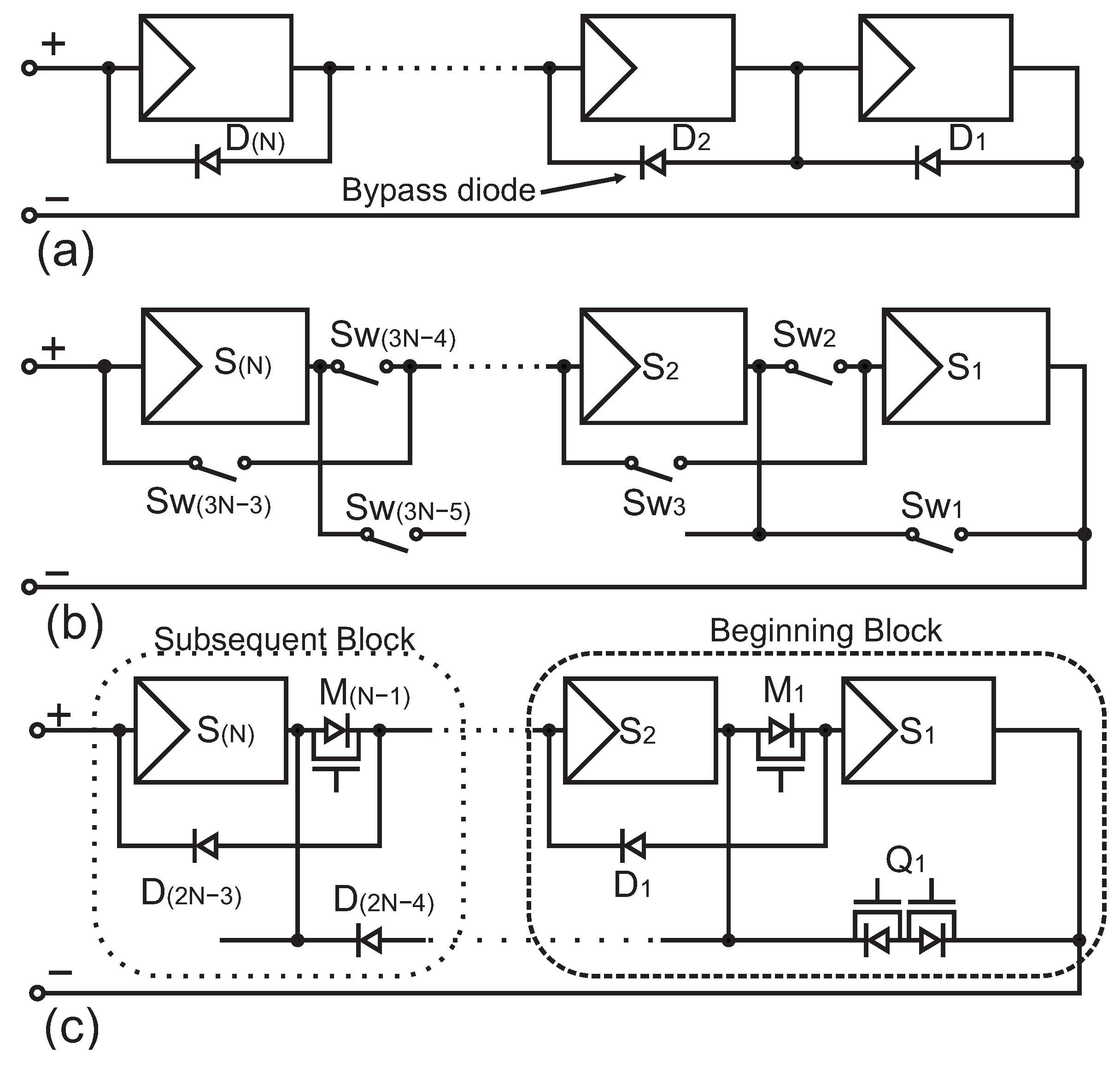
Figure 1. The schematic of (a) a number of N PV modules connected in series with bypass diode, (b) a number of N PV modules connected with switches that allow reconfiguration, and (c) the newly proposed PV array reconfiguration network implementation.
Energies 18 05866 g001
Figure 2. The PV system consists of a number of N PV modules switch circuit with parallel connections, and sensing signals highlighted.
Energies 18 05866 g002
Figure 3. Current flow between adjacent PV modules in series and parallel connections.
Energies 18 05866 g003
Figure 4. A typical IV (a) and PV (b) curve of a module under difference irradiance.
Energies 18 05866 g004
Figure 5. Flow chart of the control logic.
Energies 18 05866 g005
Figure 6. Flow chart of series to parallel conversion sub-flow.
Energies 18 05866 g006
Figure 7. PV system with 4 modules reconfiguration examples.
Energies 18 05866 g007
Figure 8. The associated PV and IV curves of the system (a) suffering partial shading and (b) having the partial shading condition removed.
Energies 18 05866 g008
Figure 9. The irradiance heat map of the solar simulator.
Energies 18 05866 g009
Figure 10. The irradiance heat map of the solar simulator overlaid with the proposed PV system under test.
Energies 18 05866 g010
Figure 11. The associated PV and IV curves of the system with (a) S 1 and S 2 , and (b) S 2 and S 3 , suffered from partial shading, and (c) normal non-shaded condition.
Energies 18 05866 g011
Table 1. Comparison of PV Reconfiguration Approaches.
CategoryFull ReconfigurationSeries-Parallel
Literature[7][1,2][5][6][3][4]This Paper
Number of PV Modules N × M N N × M NNNN
Increment of ModuleN or M11N or M111
Component CountSwitchTransistor: N × M 1 Transistor: N ( N + 3 ) 2 Electromech. relayTransistor: N × M 1 Diode: N + M Transistor: 3 N 3 Transistor: 3 N 3 Transistor: 3 N 3   2 N 2 act as passive diode
Passive Component000Capacitor: N000
Minimum Module Number22min. of 2 in N , M 2222
Required Sensor N × M Voltage N × M Current1 Voltage 1 CurrentUndetermined1 Voltage 1 CurrentN Voltage 2 N 2 Current N Voltage 1 Current (shared MPPT)
Reaction TimeFault detectionReal-timeSlow intervalUndeterminedReal-time with slow MPPTNot availableReal-timeReal-time
Fault removalReal-timeSlow intervalUndeterminedReal-time with slow MPPTPeriodicPeriodicReal-time
Configuration FlexibilityAny config.Any config.Highly limitedLimitedLimited parallel/series
Energy LossConduction lossConduction lossConduction lossConduction lossConduction + Switching lossConduction lossConduction loss
Primary AimsPartial Shading, Fault eliminationPartial Shading, FaultPartial Shading, FaultFault (check shading)Wide Output Voltage RangePartial Shading, FaultPartial Shading, Fault
ApplicationsLarge-scale PVRooftop and large-scale PVRooftop and large-scale PVRooftop and large-scale PVBattery-powered deviceRooftop and large-scale PVRooftop and large-scale PV
Table 2. The operating conditions of the PV system for control signal explanation.
Series to ParallelParallel to Series
Irradiance on modules S 1 1000 W/m21000 W/m2
S 2 600 W/m21000 W/m2
S 3 600 W/m21000 W/m2
S 4 1000 W/m21000 W/m2
Voltage levels at MPP V 1 43.8 V41.06 V
V 2 84.0 V40.94 V
V 3 124.2 V85.09 V
V 4 168.0 V126.15 V
Current at MPPI5.48 A9.04 A
Activated Switches M 1 , M 2 , M 3 D 1 , D 2 , D 3 , M 1 , M 3
Table 3. Characteristics of the PV module under test.
NamePanel: Karra 350Module: 1/3 of Panel
Rated Power ( P m a x )350 W116 W
Rated Power Voltage ( V m p )37.55 V12.5 V
Rated Power Current ( I m p )9.32 A9.32 A
Open Circuit Voltage ( V o c )45 V15 V
Short Circuit Current ( I s c )9.94 A9.94 A
Total Number of Cells6622
Dimension1827 × 1000 mm1827 × 333 mm
Table 4. The operating conditions of the PV system in the example.
Condition 1Condition 2
Before ReconfigureAfter ReconfigureBefore ReconfigureAfter Reconfigure
Irradiance on modules S 1 1000 W/m21000 W/m2
S 2 800 W/m21000 W/m2
S 3 500 W/m21000 W/m2
S 4 300 W/m21000 W/m2
Voltage levels at MPP V 1 37.14 V 24.17  mV 25.14  mV40.21 V
V 2 80.40 V38.63 V44.02 V80.42 V
V 3 124.7 V79.06 V83.75 V120.63 V
V 4 169.4 V121.99 V123.51 V160.86 V
Current at MPPI2.73 A7.34 A9.40 A9.31 A
Activated Switches M 1 , M 2 , M 3 Q 1 , D 1 , M 2 , M 3 Q 1 , D 1 , M 2 , M 3 M 1 , M 2 , M 3
Disclaimer/Publisher’s Note: The statements, opinions and data contained in all publications are solely those of the individual author(s) and contributor(s) and not of MDPI and/or the editor(s). MDPI and/or the editor(s) disclaim responsibility for any injury to people or property resulting from any ideas, methods, instructions or products referred to in the content.