1. Introduction
The past decade has witnessed a paradigm shift in the transportation and mobility sectors, primarily driven by stringent greenhouse gas emission regulations and rapid advancements in battery technologies. The resultant decrease in battery manufacturing costs has enabled widespread adoption of electric propulsion systems across industries such as automotive, aerospace, and advanced robotics. This transformation has created a pressing need for compact, lightweight, and energy-efficient power electronic converters, which are central to the operation of electric motor drives.
In mobile platforms, reducing the size and weight of motor drives is not merely a design preference but a crucial factor in system-level efficiency. Lower power losses directly translate to reduced energy drawn from the battery pack, enabling downsizing of the battery itself. Such cascading benefits—lighter battery packs reducing total vehicle mass and, in turn, lowering energy consumption—underscore the strategic importance of highly efficient motor drive systems.
Recent advances in semiconductor technology have positioned WBG devices, particularly SiC and GaN, as transformative solutions for next-generation power converters [
1]. Compared to traditional silicon switches, WBG devices exhibit superior material characteristics, including higher breakdown voltages, elevated thermal conductivity, and the ability to operate at significantly higher switching frequencies. These attributes enable drastic reductions in conduction and switching losses, increased power density, and the use of smaller passive components, which collectively enhance drive performance in weight-sensitive applications [
2]. A notable example is the use of SiC MOSFETs in the powertrain of Tesla Model 3 electric vehicle, which achieves an estimated 2–3% improvement in inverter efficiency while significantly reducing system weight to approximately 4.8 kg—less than half that of similar silicon-based inverters [
3].
Despite these advantages, the deployment of WBG devices introduces nontrivial challenges that must be addressed to ensure reliable long-term operation. The ultra-fast switching transitions inherent to SiC and GaN transistors produce steep voltage slew rates (high dv/dt), which intensify electromagnetic interference (EMI) and introduce complex insulation stress mechanisms within electric machines. In systems employing inverter-motor power cables, traveling wave reflections can lead to terminal overvoltage that may approach or even exceed twice the applied dc-link voltage [
4]. These repetitive overvoltages accelerate the partial discharge phenomenon and degrade stator winding insulation, significantly shortening motor lifetime.
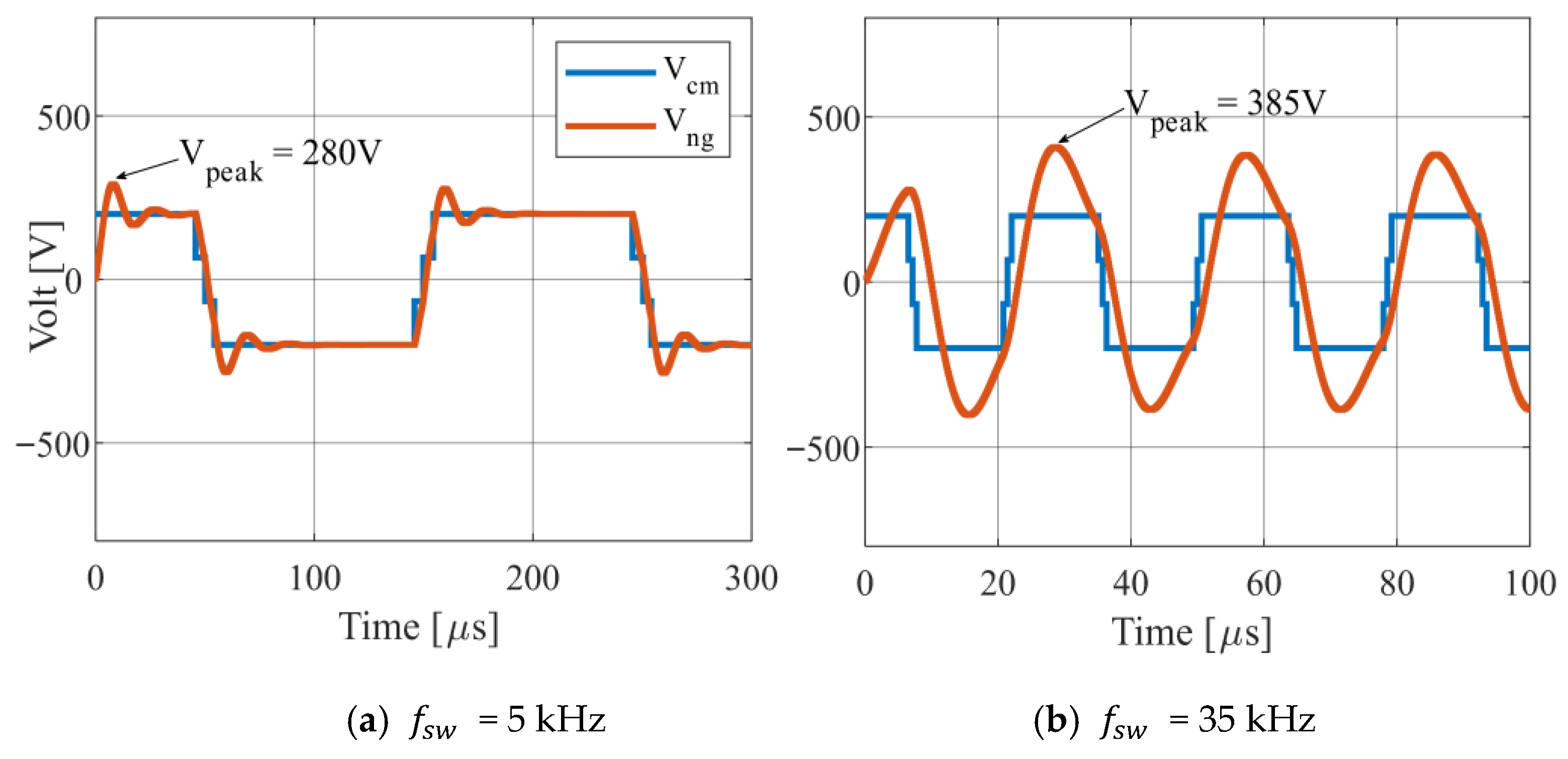
Moreover, high dv/dt CM voltage generated by WBG inverters contributes to the overvoltage appearing at the motor stator neutral point. The latest research in [
5,
6] indicates that motor neutral point overvoltage can pose greater risks than motor terminal overvoltage to motor windings as well as bearings, which in turn leads to premature motor failure. Motor neutral point overvoltage is caused by the propagation of inverter CM voltage through machine windings. Since the motor neutral point is typically floating, the CM voltage encounters an infinite impedance at the neutral point (due to a very small winding-to-frame parasitic capacitance), where the impedance mismatch between the motor surge impedance and the neutral point parasitic capacitive reactance results in overvoltage oscillations at the motor neutral point, a phenomenon known as the reflected wave effect [
5]. It is pertinent to note that the motor neutral point overvoltage oscillations are characterized by the 1st antiresonance frequency of the motor, which is solely the function of machine CM winding inductance and its parasitic capacitances. Hence, the neutral point overvoltage, unlike motor terminal overvoltage, is independent of the cable length where this type of overvoltage can be observed without any cable connected between the inverter and motor [
5]. Given that the 1st antiresonance frequency of the motor typically falls within the kHz range [
6], the use of high-frequency WBG devices can enable the drive switching frequency or its harmonics to coincide with the motor 1st antiresonance frequency. Unlike inverter CM voltage, the magnitude of motor neutral point voltage is influenced by the relationship between drive switching frequency and machine antiresonance frequency. As the switching frequency approaches the machine antiresonance frequency, the neutral point voltage increases. Furthermore, if both frequencies align, the overvoltage can increase significantly, exceeding CM voltage by several times due to motor resonance excitation [
6].
This resonance effect is typically negligible with conventional silicon IGBT inverters, as their switching frequency is practically limited to 20 kHz, while motor antiresonance frequency is usually above 40 kHz [
7]. However, with the rise of WBG devices, switching frequencies can now reach up to 200 kHz with SiC MOSFETs and even higher with GaN devices [
8], increasing the likelihood of switching frequency or its harmonics matching the motor antiresonance frequency. As a result, an elevated neutral point voltage can impose considerable electrical stress on the winding turns closer to the stator neutral point, increasing the risk of insulation failure. Additionally, it directly affects the magnitude of bearing voltage, resulting in higher bearing current levels and accelerated bearing degradation.
CM chokes are widely utilized as a simple and highly effective approach to improve the motor drive performance by attenuating the CM noise and EMI in conventional variable speed drives. The conventional CM choke inductance is selected to create a high impedance in the CM current path within the desired frequency range, limiting the CM current flow to motor windings and frame. This ensures that CM current and EMI levels remain within the limits of safety standards. However, conventional choke designs have negligible impact on bearing current mitigation, as they do not address the fundamental causes of bearing currents, i.e., neutral point and bearing voltage.
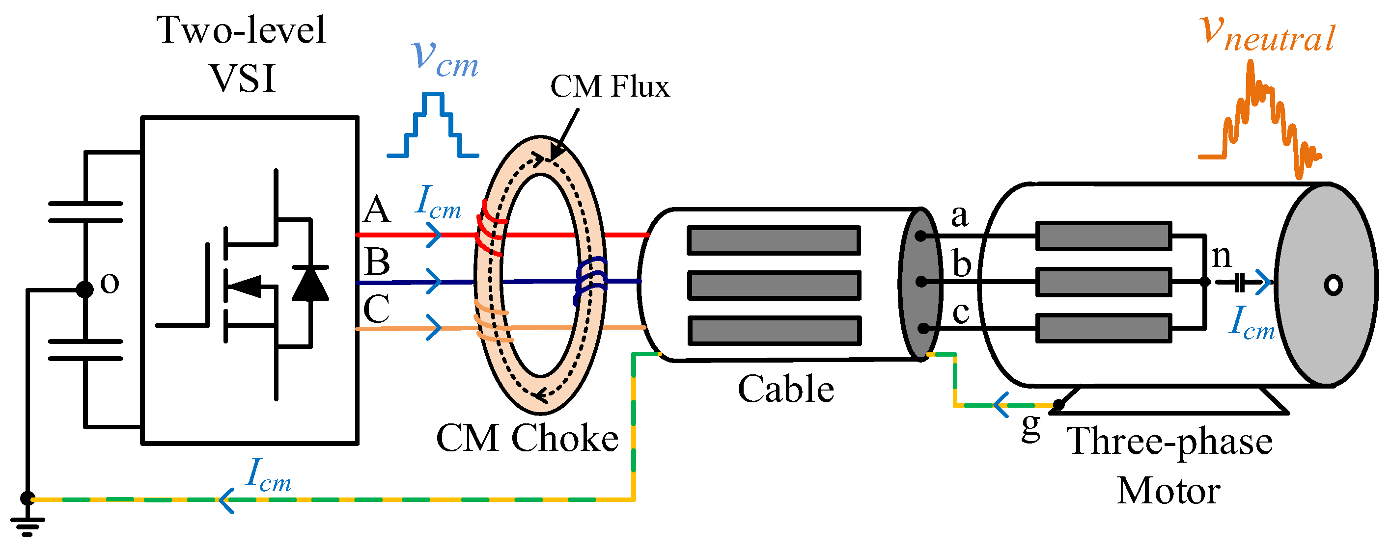
Figure 1 shows a typical motor drive system with the connection of a CM choke at the inverter terminals. It also demonstrates the CM current path and overvoltage oscillations between motor neutral point and grounded frame. In
Figure 1, the two-level voltage-source inverter (VSI) supplies a three-phase star-connected motor through a four-core power cable. The three output terminals of the VSI (A, B, and C) are connected to the corresponding motor terminals (a, b, and c) through a CM choke and power cable, while the dc-link midpoint (O) is connected to the grounded motor frame (g). Since the CM current
flows in the same direction in all three phases, the CM fluxes add up in the choke core and provide a high impedance to
, while allowing the line current to pass through with negligible impedance.
While CM current and EMI mitigation remains important, studies have reported that 67% of motor failures are linked to bearing-related issues [
9], resulting in costly repairs, operational downtime, and lost production in industries. This challenge has become even more critical with the increasing adoption of WBG inverter-fed motor drives in electric vehicles (EVs). In recent years, various motor bearing failures attributed to bearing voltages and EDM currents have been reported in EVs [
10]. These failures contribute to bearing instability, excessive vibration, and noise, which not only degrade the performance but can also escalate into severe mechanical failures, posing significant reliability concerns for such advanced systems where the highest level of reliability is essential. Therefore, effective strategies to mitigate bearing currents are important to ensure the longevity and reliability of wide-bandgap inverter-fed motor drives, particularly in critical applications such as EVs.
The conventional CM choke design to reduce the CM noise in variable-speed drives has been extensively studied in the literature for many years [
11]. Various aspects of CM choke inductor design and performance have also been analyzed [
12]. However, conventionally designed CM chokes are unable to mitigate motor neutral point voltage and corresponding bearing voltage and EDM bearing current. Experiments conducted in [
13] evaluate the impact of different CM chokes on CM voltage and current, bearing voltage, and EDM bearing current. While the results confirm that CM chokes can reduce CM current by up to 90%, their influence on CM voltage, bearing voltage, and EDM current remains negligible. Additionally, in [
14], various CM voltage mitigation techniques are evaluated, including the use of CM chokes. The analysis considers both the physical size and placement of the CM chokes within the motor drive system. The experimental results demonstrate that CM chokes are ineffective in reducing CM voltage, irrespective of their positioning.
EDM bearing current events are produced when the bearing voltage exceeds the dielectric breakdown threshold of the bearing lubricant. As the bearing voltage magnitude is predominantly governed by neutral point voltage, which in turn is largely driven by the inverter-generated CM voltage, it is worth exploring the CM voltage reduction techniques reported in the literature as potential solutions for mitigating EDM bearing currents. These include modified PWM schemes, modified inverter topologies, active noise cancellation circuits, soft switching inverters, and multilevel converters. The modified PWM strategies, such as active zero state PWM (AZSPWM) and near state PWM (NSPWM), reshape switching sequences to eliminate zero voltage vector generation [
15,
16,
17], whereas modified inverter topologies commonly referred to as H7 and H8 architectures [
18,
19] or multilevel converters such as T-Type or neutral point clamped [
20] inherently synthesize output voltages with reduced CM voltage through additional switching states and voltage levels, respectively. Furthermore, active noise cancellation circuits inject compensating voltages to counteract CM disturbances [
21], while soft-switching inverters mitigate high dv/dt transitions, thereby lowering CM voltage excitation [
22]. A summary of existing methods and their limitations is presented in
Table 1.
It is worth noting that the aforementioned CM voltage reduction methods are limited in their ability to reduce the CM voltage to without having additional operational constraints. Although reducing the CM voltage by 66% can suppress the bearing currents, EDM current spikes can still be observed due to the presence of overvoltage at the motor neutral point, especially when the switching frequency approaches the machine antiresonance frequency. Therefore, the CM voltage reduction methods may not be effective in eliminating the EDM current when applied to WBG inverters.
This paper proposes an alternate approach to design a CM choke for eliminating EDM bearing current. Since the added CM choke increases the inductance of the motor CM circuit, it is leveraged to shift the motor antiresonance frequency below the switching frequency to lower the voltage stress at the motor neutral point and bearings. Furthermore, by adjusting the ratio between antiresonance and switching frequency, motor bearing voltage can be reduced to a negligible value, thereby eliminating the EDM bearing current spikes. Additionally, the proposed CM choke design inherently reduces CM current magnitude and EMI by lowering the motor neutral point voltage, which serves as the primary source of CM currents. It is worth noting that the proposed CM choke only modifies the CM circuit of the motor, whereas the motor DM circuit remains unaffected. Design equations for selecting the optimal CM choke inductance and core are presented, while the effectiveness of the proposed strategy is validated through experimental testing on a 2.2 kW three-phase induction motor.
The contributions of this paper are as follows:
Comprehensive explanation of non-linear behavior of bearing voltage and the corresponding EDM bearing current events in relation to drive switching frequency, offering deeper insight into the underlying mechanisms.
Analysis of the limitation of conventional choke design approach.
An alternative choke design approach to prevent the machine’s antiresonance frequency from approaching or coinciding with the drive switching frequency, thereby avoiding the excitation of motor resonance that exacerbates bearing current.
The proposed approach eliminates the EDM currents under all tested scenarios, regardless of switching frequency or dc-link voltage.
Experimental evaluation of the proposed choke design approach against existing CM voltage reduction methods to highlight its superior performance.
The rest of the paper is structured as follows.
Section 2 highlights the limitation of conventional CM choke design.
Section 3 defines the bearing voltage and experimentally analyzes its influencing factors. In
Section 4, the different types of bearing currents are demonstrated, while EDM bearing current and its influencing factors are experimentally elaborated.
Section 5 presents the design equations for selecting CM choke inductance and core to eliminate EDM bearing current.
Section 6 outlines the employed experimental approach in this work, detailing the methodologies used to evaluate the proposed choke design. Finally,
Section 7 concludes the paper.
3. Motor Bearing Voltage and Its Influencing Factors
Bearing voltage, defined as the potential difference between the inner and outer races of motor bearings, has long been recognized as a critical reliability concern in electric motor drives [
24]. The adoption of WBG semiconductor devices has further exacerbated its severity, as the higher switching frequencies enabled by WBG inverters intensify neutral point overvoltage. This results in an increase in the dielectric stress across the bearing lubricant layer, promoting harmful discharge currents that accelerate surface degradation and significantly increase the risk of premature bearing and motor failure.
Electric motors inherently exhibit various parasitic capacitances distributed across different components, including the stator windings, rotor, and bearings. In high-switching-frequency motor drives, these capacitances can provide a low-impedance path, resulting in leakage currents flowing through both the motor frame and the bearings. Furthermore, the winding-to-frame capacitance couples the CM voltage to the motor frame, creating the motor neutral-point potential relative to ground. Simultaneously, the bearing capacitance establishes a capacitive path between the rotor and stator frame, resulting in a voltage difference across the inner and outer bearing races.
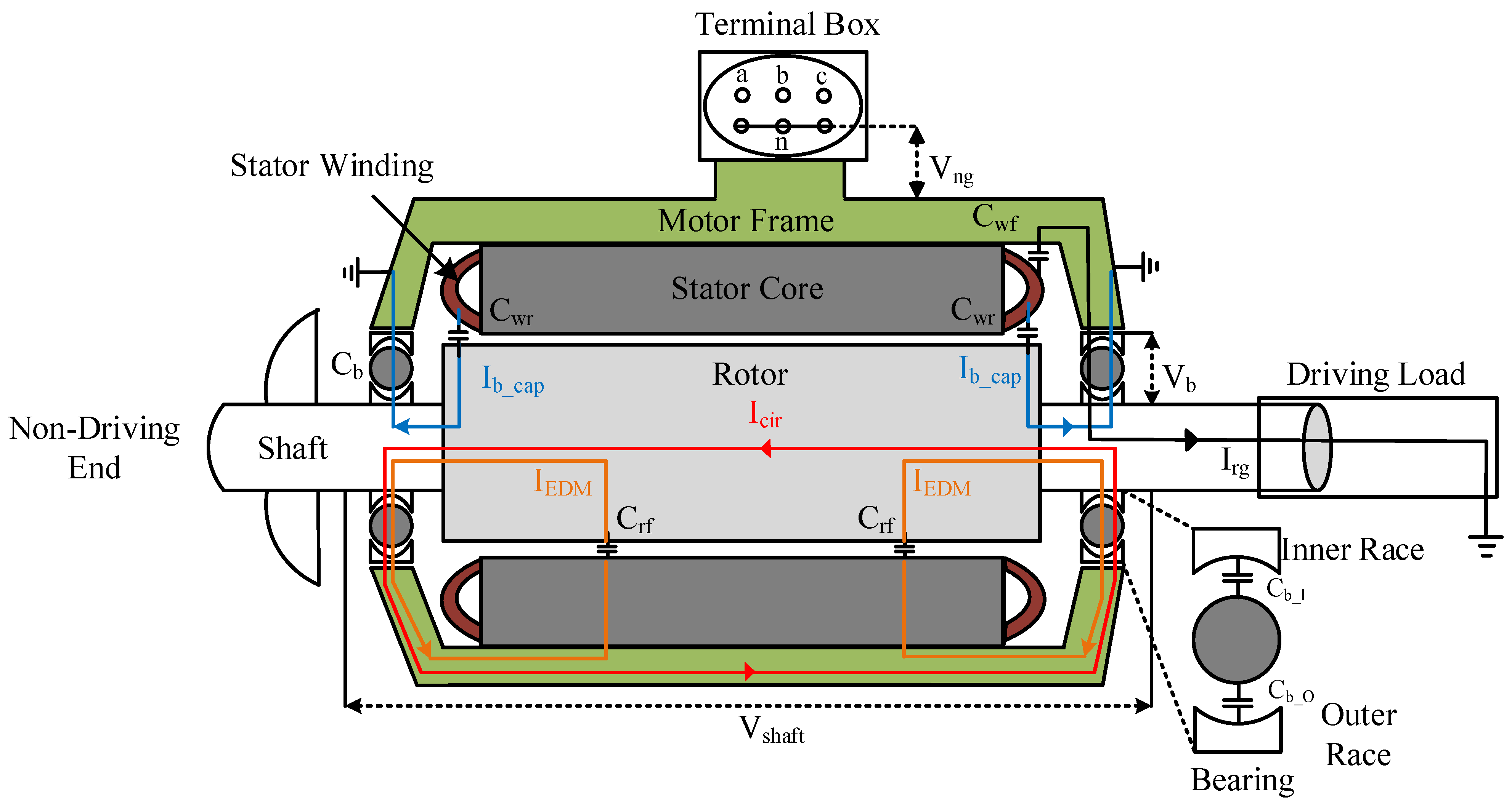
Figure 7 shows the cross-sectional view of a three-phase star-connected motor, highlighting the different parasitic capacitances distributed throughout the machine. It also highlights the voltages that arise between different motor components, which contribute to the generation of bearing currents. The parasitic capacitances present within the motor are the capacitance from stator winding to grounded frame
stator winding to rotor
, rotor to grounded frame
, and bearing capacitance
. The motor bearing capacitance
consists of
and
, which represent the capacitances from the inner and outer bearing race to the rolling element (ball), respectively. These inner and outer bearing capacitances combine to form the total bearing capacitance, expressed as
(i.e.,
).
In the existing literature, the terms “bearing voltage” and “shaft voltage” are used interchangeably. However, there is a significant difference between the two voltages. The bearing voltage
is defined as the potential difference between the inner and outer races of the bearing (i.e., between shaft and grounded frame), while the shaft voltage
represents the potential difference between the driving end and non-driving end bearings [
24]. These voltages are directly affected by neutral point voltage
, which is the voltage between the stator winding neutral point and the grounded frame of the motor, as shown in
Figure 7. This voltage is typically assumed to be equal to the inverter CM voltage. However, in the previous section, it was demonstrated that it can be several times higher than the CM voltage, depending on the drive switching frequency. This observation underscores the need for a detailed investigation into the influence of switching frequency on bearing voltage formation.
3.1. Impact of Switching Frequency
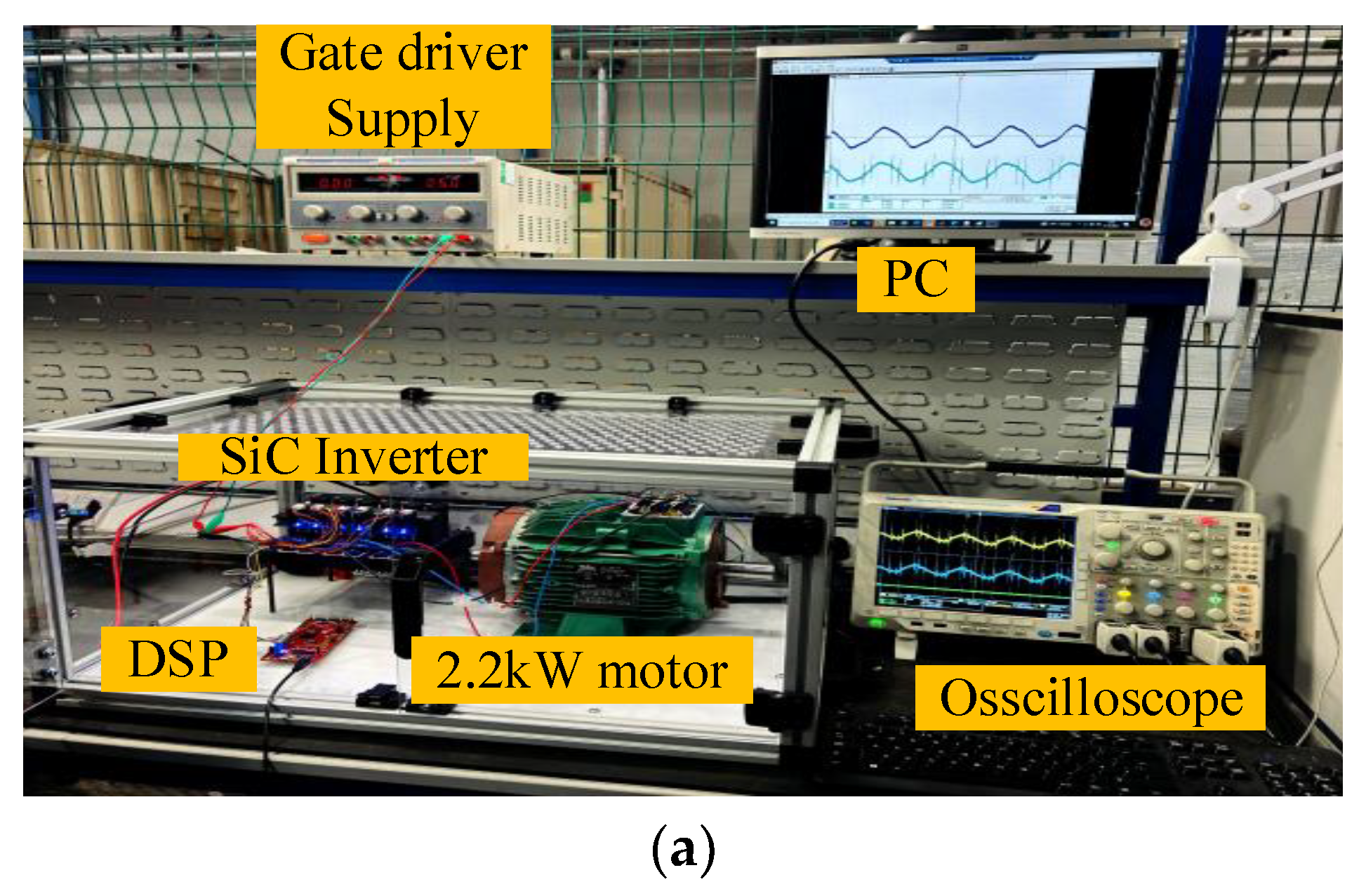
To observe the effect of switching frequency on bearing voltage, experimental analysis is carried out on a 2.2 kW three-phase four pole star-connected induction motor supplied by a three-phase SiC two-level VSI, as shown in the experimental setup in
Figure 8a. Experimental parameters of the inverter, motor, and measurement probes are listed in
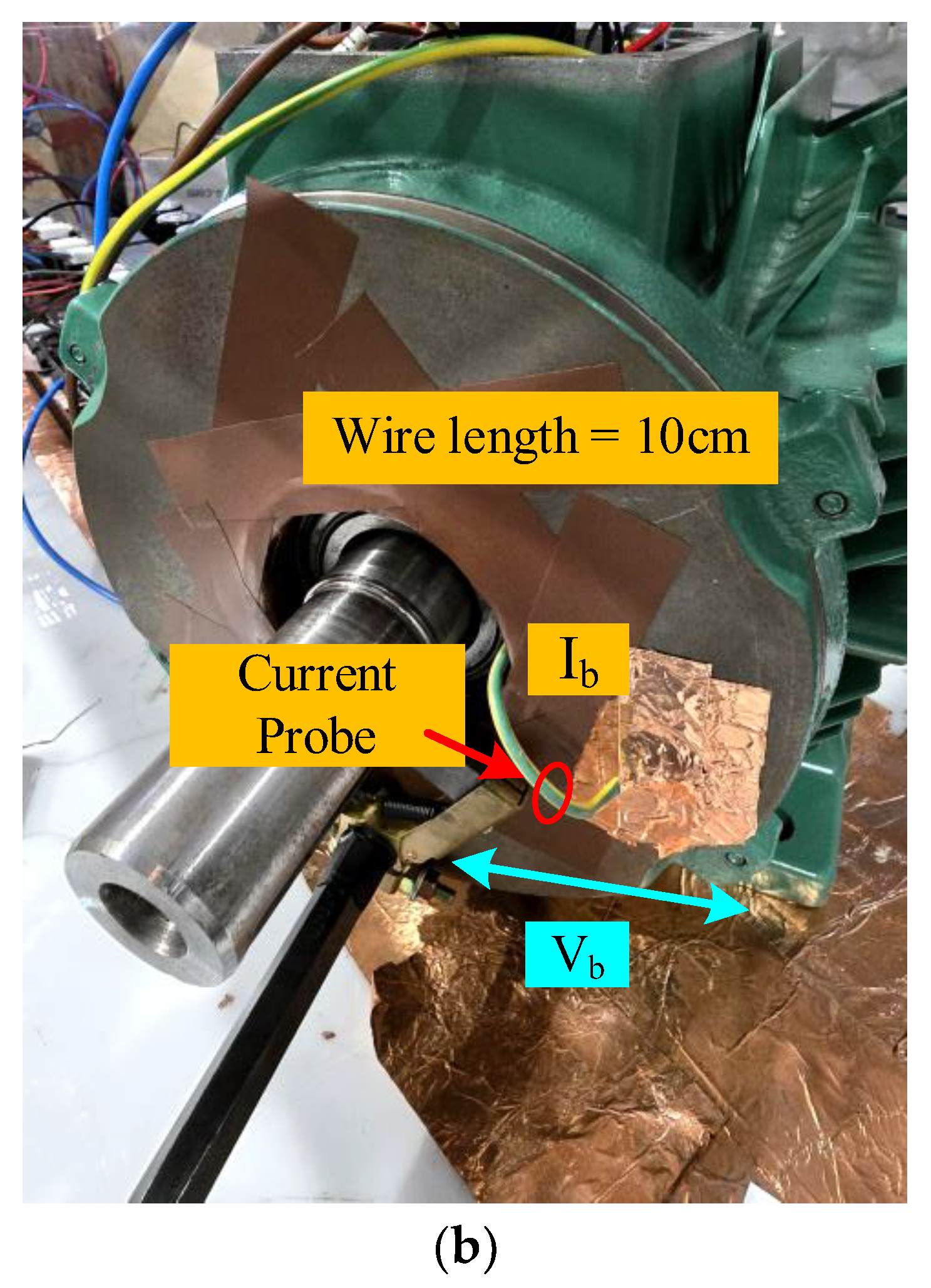
Table 2. The CM voltage is calculated by averaging the three pole voltages of the inverter, while the neutral point voltage is measured between stator neutral point and grounded motor frame. On the other hand, the bearing voltage is measured between the rotor shaft and ground by using a carbon brush and a V-shaped brush holder, as shown in
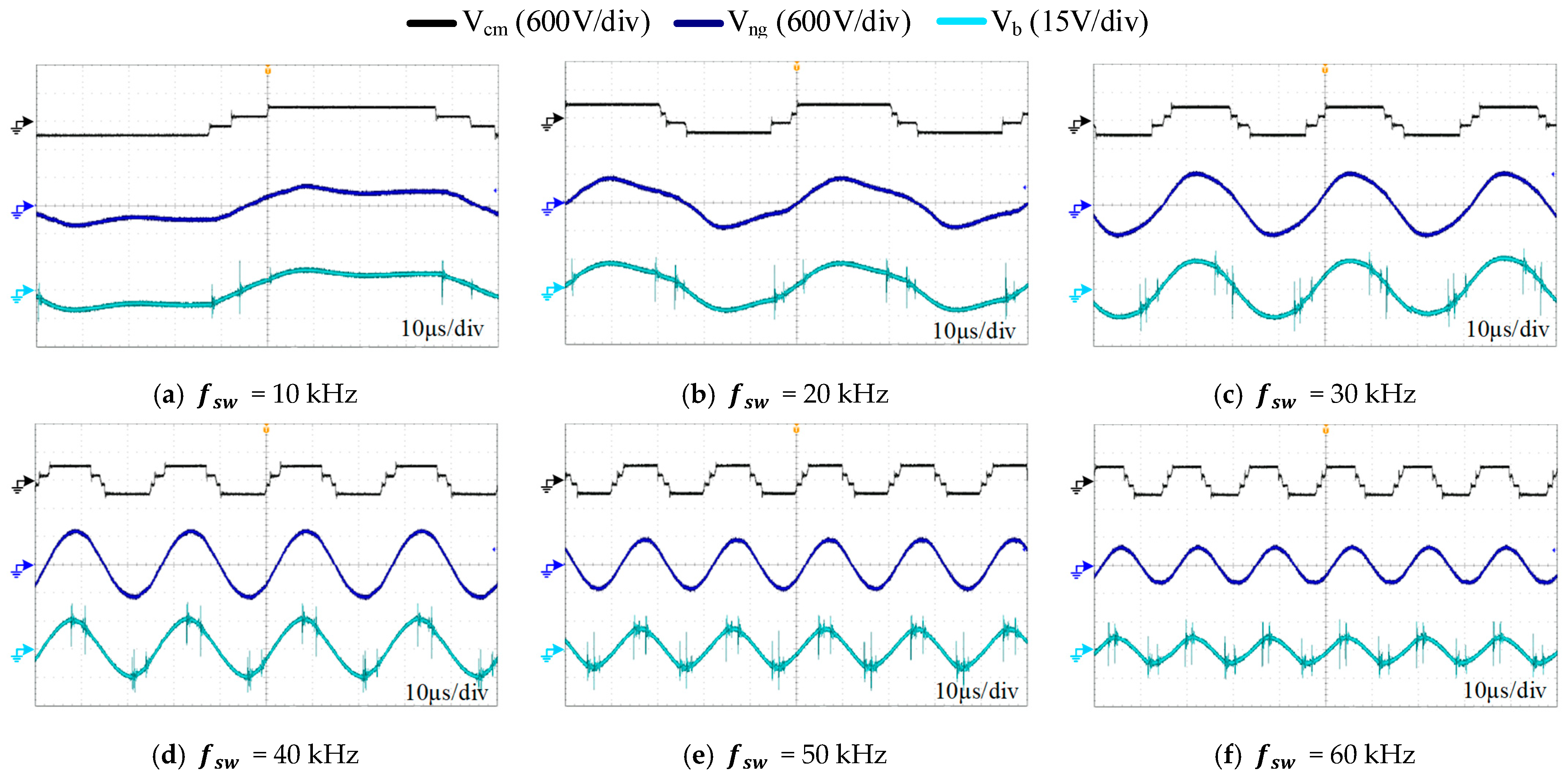
Figure 8b. The inverter is supplied with a constant dc-link voltage of 600 V at a modulation index of 0.3. The switching frequency
is increased from 10 kHz to 60 kHz, and the corresponding effect on
,
, and
is analyzed. The results are presented in
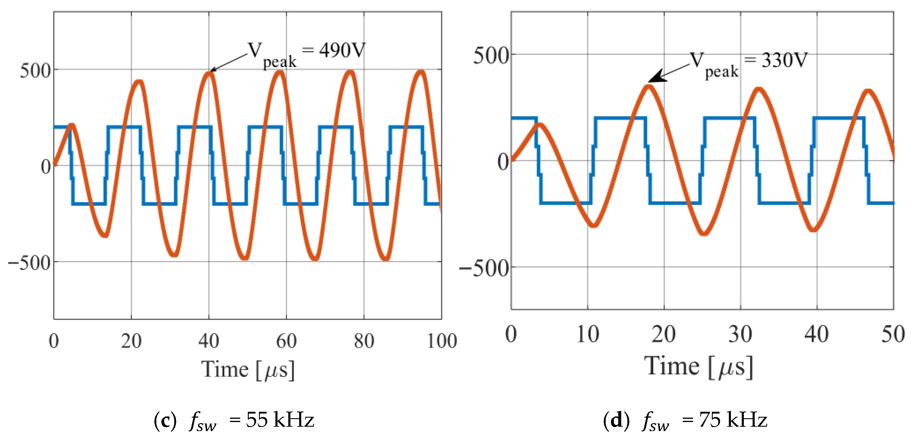
Figure 9, showing how the switching frequency variations impact the motor neutral point voltage and bearing voltage, where they have distinct behaviors, exhibiting peaks that increase/decrease under certain changes in the switching frequency, whereas the CM voltage peak remains constant at 300 V. At low switching frequency, i.e., 10 kHz (see
Figure 9a), the bearing voltage and neutral point voltage traverse in different voltage levels almost equivalent to the CM voltage. However, as the switching frequency increases, as shown in subsequent subplots of
Figure 9,
and
become almost sinusoidal due to the increasing filtering effect of motor parasitic capacitances. This again proves that the bearing voltage is directly influenced by the neutral point voltage rather than the CM voltage. Additionally, it can be observed from
Figure 10, which summarizes the data collected from
Figure 9, that the peak values of both
and
increase as the switching frequency rises from 10 kHz to 40 kHz, after which these values begin to decrease.
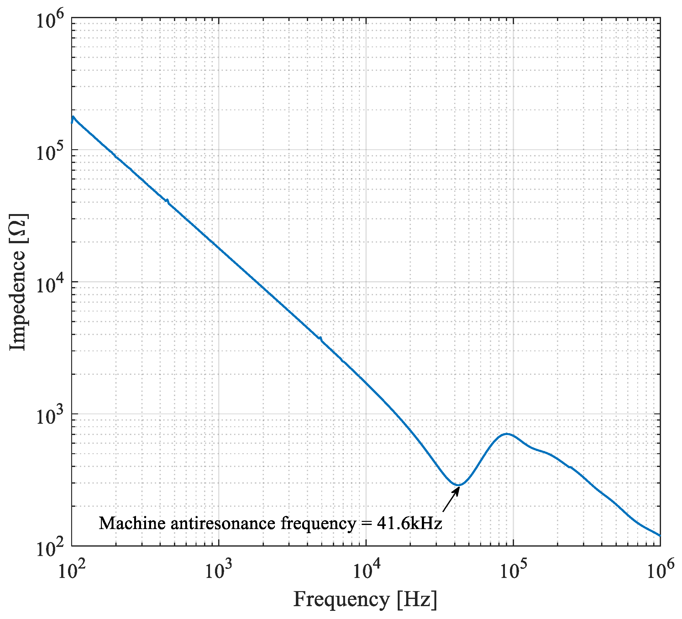
To explain this phenomenon, it is important to consider the machine antiresonance frequency, which can be determined by measuring machine CM impedance between the parallel-connected three phases and ground wire of the motor. To measure the CM impedance of the motor under test, an impedance analyzer Soletron (1260 + 1287) is utilized, and the corresponding CM impedance graph is shown in
Figure 11. The machine antiresonance frequency is observed at 41.6 kHz. The motor neutral point voltage, due to its capacitive nature, increases when the switching frequency is below the machine antiresonance frequency (i.e.,
< 41.6 kHz) (see
Figure 9a–d and
Figure 10) and decreases when the switching frequency exceeds the antiresonance point (i.e.,
> 41.6 kHz) (see
Figure 9e,f and
Figure 10). A similar trend can be observed in the bearing voltage. The reduction in bearing voltage after the antiresonance point inherently leads to a corresponding reduction in EDM currents, as it is unable to break down the bearing oil film.
3.2. Impact of Dc-Link Voltage
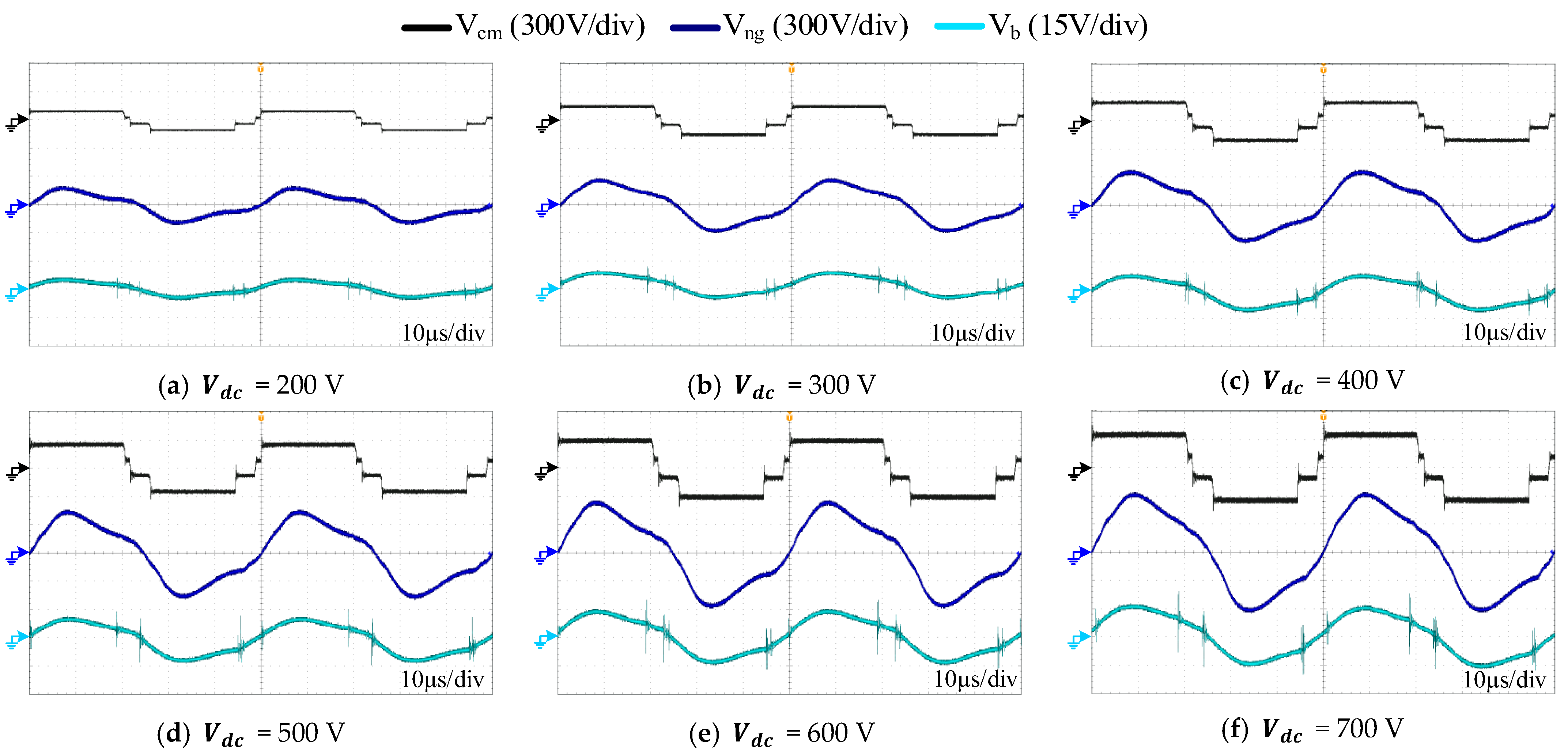
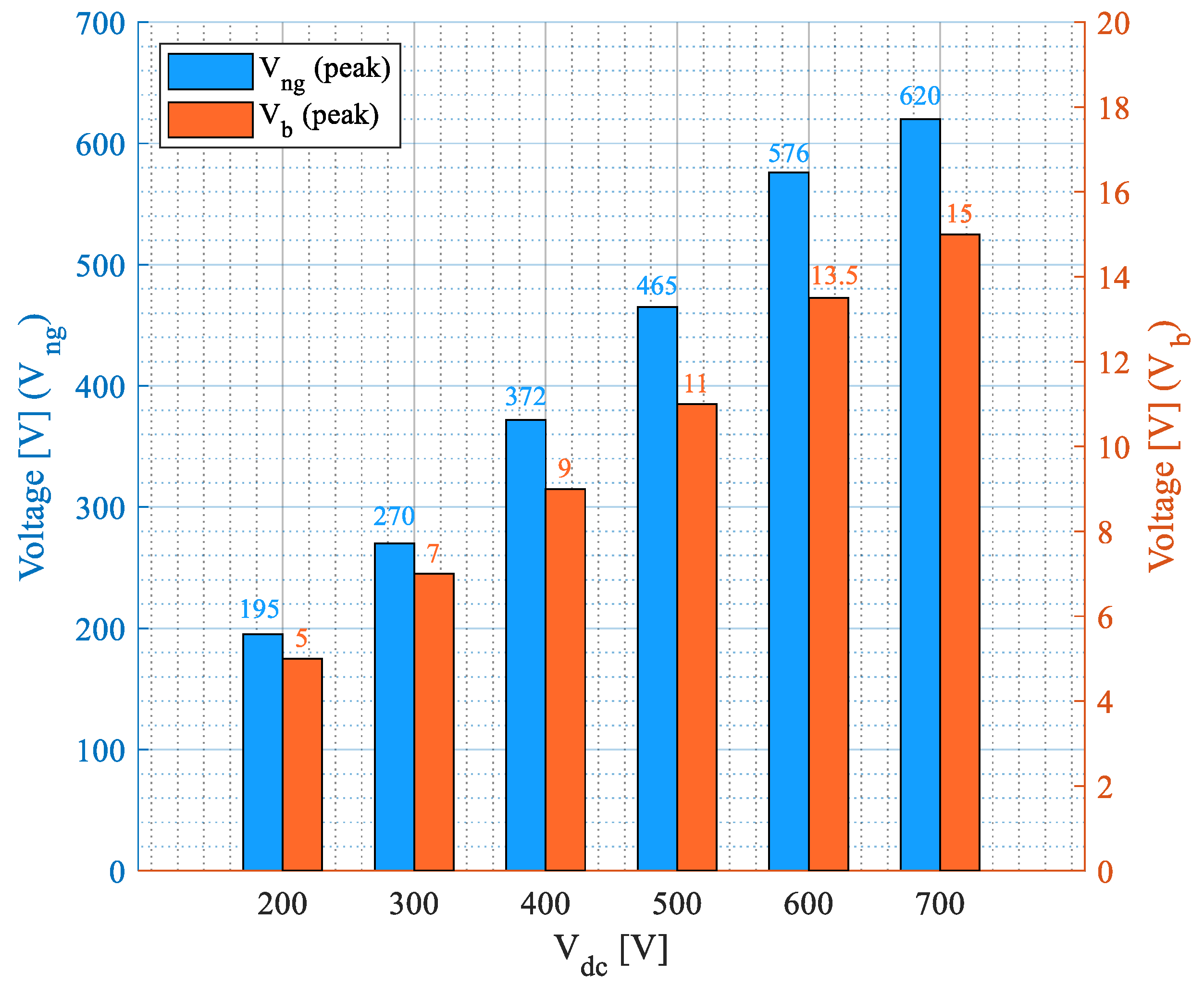
To evaluate the effect of dc-link voltage on bearing voltage, the motor drive is operated at a fixed switching frequency of 20 kHz and a modulation index of 0.3, while the dc-link voltage is varied from 200 V to 700 V. The motor neutral point voltage and bearing voltage are measured and illustrated in
Figure 12. Furthermore, the peak neutral point and bearing voltage values at different dc-link voltages are summarized in
Figure 13. As observed, both the neutral point voltage and bearing voltage are directly proportional to the dc-link voltage. This phenomenon is attributed to the neutral point voltage being derived from the CM voltage generated by the inverter. As the dc-link voltage increases, the CM voltage correspondingly rises, causing an increase in both the neutral point and bearing voltages. At a low dc-link voltage of 200 V (see
Figure 12a and
Figure 13), the peak neutral point voltage and peak bearing voltage are approximately 195 V and 5 V, respectively (i.e.,
= 1.95 pu). As the dc-link voltage is increased in the subsequent subplots in 100 V steps up to 700 V (see
Figure 12b–f and
Figure 13), the neutral point and bearing voltages are observed to increase almost linearly from 195 V to 620 V and 5 V to 15 V, respectively. Since the switching frequency, i.e., 20 kHz, is kept constant at a value far away from motor antiresonance frequency, i.e., 41.6 kHz, the ratio of peak neutral point voltage to peak CM voltage remains almost constant at approximately 1.8–1.9 pu across all dc-link voltages, whereas, in the case of switching frequency matching the machine antiresonance frequency, this ratio was observed as approximately 2.5 pu (see
Figure 10). Notably, even at the lowest dc-link voltage of 200 V (i.e., 100 V CM voltage) and a low switching frequency of 20 kHz (away from motor antiresonance frequency), the peak bearing voltage reaches 5 V, which is sufficient to compromise the bearing lubricant film and initiate EDM currents depending upon the bearing geometry and size. Therefore, any mitigation strategy must be designed to consider the influence of dc-link voltage alongside switching frequency to effectively reduce EDM bearing currents.
4. Electrostatic Discharge Machining Bearing Currents
Conventional CM choke designs primarily target the mitigation of CM grounding currents flowing from the stator winding to the grounded motor frame through parasitic capacitances. However, additional grounding currents, known as bearing currents, also exist within the motor. These currents flow from the stator winding to the rotor, and subsequently from the rotor shaft to the grounded motor frame via the motor bearings. In this research, the choke design is specifically focused on reducing bearing currents. An added benefit of the proposed design is its inherent ability to reduce CM grounding currents as well, achieved through the reduction of the motor neutral point voltage and bearing voltage, which acts as the primary driver of CM currents.
Various circulating and non-circulating bearing currents exist within the motor, as demonstrated in
Figure 7. High-frequency circulating and EDM bearing currents flow within a closed loop, whereas rotor grounding and dv/dt capacitive bearing currents originate from the motor windings and discharge to the grounded motor frame. The high-frequency circulating bearing current
circulates between the stator frame and rotor shaft through the bearings. Similarly, the EDM current
forms a loop beginning at the rotor shaft, traveling through the bearings to the stator frame, continuing to the stator core, and then reaching the rotor core via the capacitance
before completing its path back to the rotor shaft. Additionally, a portion of the total CM grounding current may be conducted as rotor ground current
, particularly when the rotor is grounded through the driven load. On the other hand, the dv/dt capacitive bearing current
flows from the winding to the rotor, then to the bearing, and finally to the grounded frame through the parasitic capacitances
and
. It is worth noting that the EDM bearing current directly penetrates the lubricating film within the bearing instead of flowing through the bearing capacitances. That is why the EDM current is a primary contributor to bearing degradation compared to the other types of bearing currents.
In the case of healthy lubrication, the bearings maintain lubricant film thickness ranging from 0.1 to 1.4 µm, capable of withstanding voltages between 1.5 and 21 V [
25]. However, when this voltage threshold is exceeded, EDM occurs within the motor bearings. This can be visualized by measuring the bearing current of the motor. There are different methods to measure bearing currents, such as direct intrusion measurement, the use of an additional bearing, or radio frequency antenna-based methods. In this paper, a direct intrusive measurement method is employed, as it allows accurate measurement of all types of bearing currents as compared to other methods.
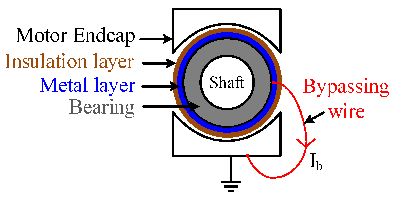
In this method, the motor’s endcap is modified to accommodate the measurement circuit, as shown in
Figure 14. The motor end cap is widened to incorporate a 1 mm thick metal layer and a 1 mm thick insulation layer. The metal layer is inserted around the bearing, and the insulation layer is positioned between the bearing and the motor frame afterwards to prevent the bearing current from flowing into the motor frame. A short wire is connected to the metal layer and taken out to allow the bearing current to bypass the original internal current flow path, thereby enabling direct measurement of the current passing through the wire. Due to the random occurrence of EDM currents, an “Edge count” function is utilized in the oscilloscope to count the number of EDM spikes. The threshold for EDM current detection is set as 100 mA which is significantly higher as compared to dv/dt bearing currents.
Figure 15 shows the bearing voltage along with the associated bearing current measured at 600 V dc-link voltage and 20 kHz switching frequency. As seen, during the EDM event, the voltage across the bearing drops to zero as the lubricant film ruptures. This rupture causes the energy stored in the rotor-to-frame capacitance to discharge through the bearings, resulting in an impulse current. The released energy generates an arc that can melt the surface of the bearing raceway. The molten material is subsequently rolled over by the rolling elements, forming a grey trace, and in severe cases, leading to a series of flutings. Some of this molten material may also mix with the bearing lubricant, impairing its insulating properties. Additionally, the rupture of the lubricant creates high temperatures that can cause the lubricant to evaporate. This transient breakdown process lasts only for a few hundred nanoseconds, before which the dielectric lubricant flows back into the gap created by the discharge, reforming a new insulating film. Consequently, the bearing capacitance recharges, and the EDM current ceases. This cycle of breakdown and recovery occurs repeatedly, impacting the bearing voltage waveform after each breakdown. Referring to
Figure 15, each time the bearing voltage drops to zero during a breakdown, the voltage waveform shifts upward or downward. A downward shift occurs if the EDM event takes place during the positive half-cycle of the bearing voltage, and vice versa. As a result of this shift, the voltage trajectory deviates from its original path during the subsequent switching event.
On the other hand, the capacitive dv/dt bearing current is generated with each switching event, as shown in
Figure 15. The frequency of occurrence of capacitive bearing current is significantly higher than that of EDM current. However, due to its relatively low amplitude (less than 100 mA), this dv/dt bearing current is generally not considered harmful to the bearing raceway. In contrast, EDM currents can range from 200 mA to 1.4 A [
26], posing a serious risk of damage to the bearing.
4.1. Impact of Switching Frequency on EDM Bearing Current
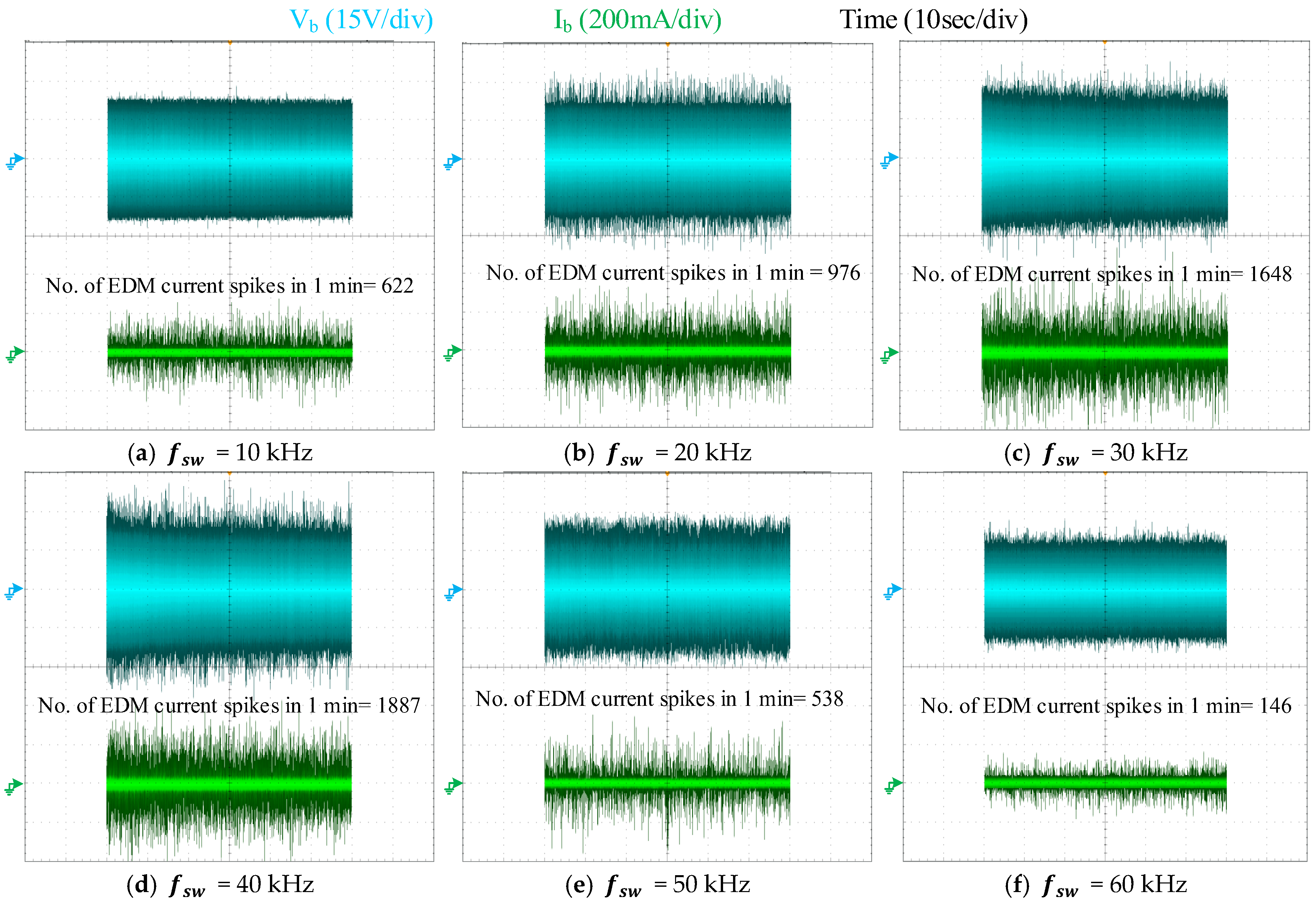
To observe the effect of switching frequency on EDM events, the motor under test is supplied by a fixed dc-link voltage of 600 V and a modulation index of 0.3, while the switching frequency is varied from 10 kHz to 60 kHz (10 kHz increment). This switching frequency range is selected to cover the antiresonance frequency of the motor under test (i.e., 41.6 kHz). The results presented in
Figure 16 demonstrate that the number of EDM current spikes, within 1 min, rises from 622 at 10 kHz to 1887 at 40 kHz, and then decreases to 146 at 60 kHz. This non-linearity can be explained by considering the machine antiresonance frequency and switching frequency of the drive.
As demonstrated in
Section 2 and
Section 3, the bearing voltage, which acts as the primary source of EDM current generation, exhibits a direct proportionality to the motor neutral point voltage, whereas the neutral point voltage itself depends on the relationship between the machine antiresonance frequency and switching frequency. Since the antiresonance frequency of the motor under test is measured as 41.6 kHz, the motor neutral point voltage increases when the switching frequency increases up to this antiresonance point.
However, when the switching frequency exceeds the machine antiresonance frequency, the neutral point voltage subsequently decreases. Since the bearing voltage directly reflects the behavior of the motor neutral point voltage, it follows a similar pattern, as demonstrated in
Figure 10. Given that EDM current occurrence is governed by the bearing voltage, the increase in switching frequency initially results in an increased EDM current count. Beyond the point where the switching frequency surpasses the machine antiresonance frequency (see
Figure 9e,f), the decrease in bearing voltage leads to a corresponding reduction in EDM current events.
4.2. Impact of Dc-Link Voltage on EDM Bearing Current
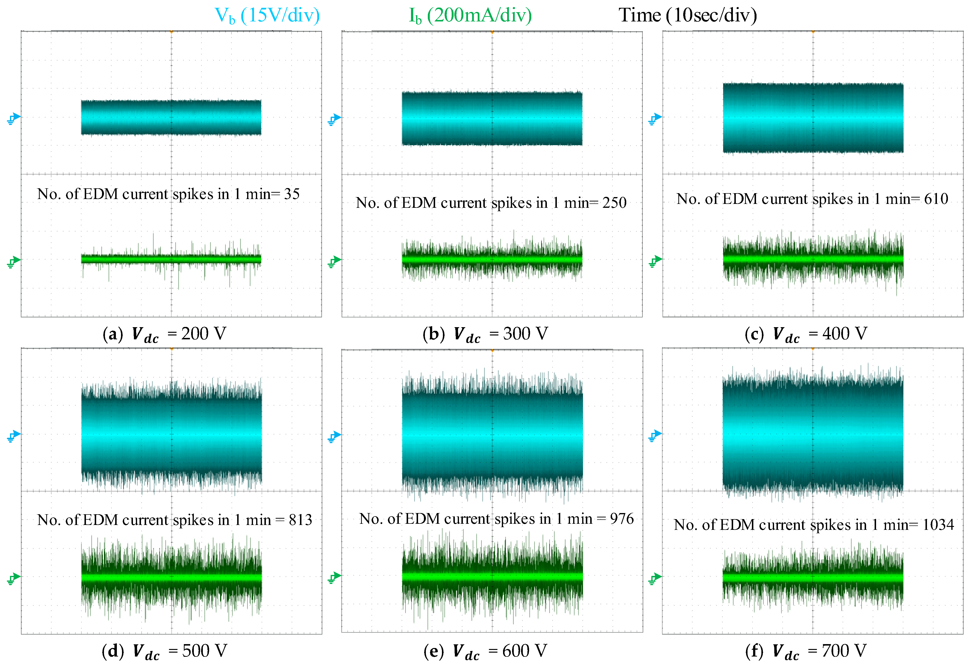
To evaluate the effect of the dc-link voltage on the EDM current, the motor is supplied at a fixed switching frequency and modulation index of 20 kHz and 0.3, respectively, while the dc-link voltage is varied from 200 V to 700 V in an increment of 100 V. The results presented in
Figure 17 show that the number of EDM events, within 1 min, increases from 35 counts at 200 V to 1034 counts at 700 V. This indicates that the increase in dc-link voltage significantly influences the EDM current events, where they increase linearly with increasing dc-link voltage even at low modulation index.
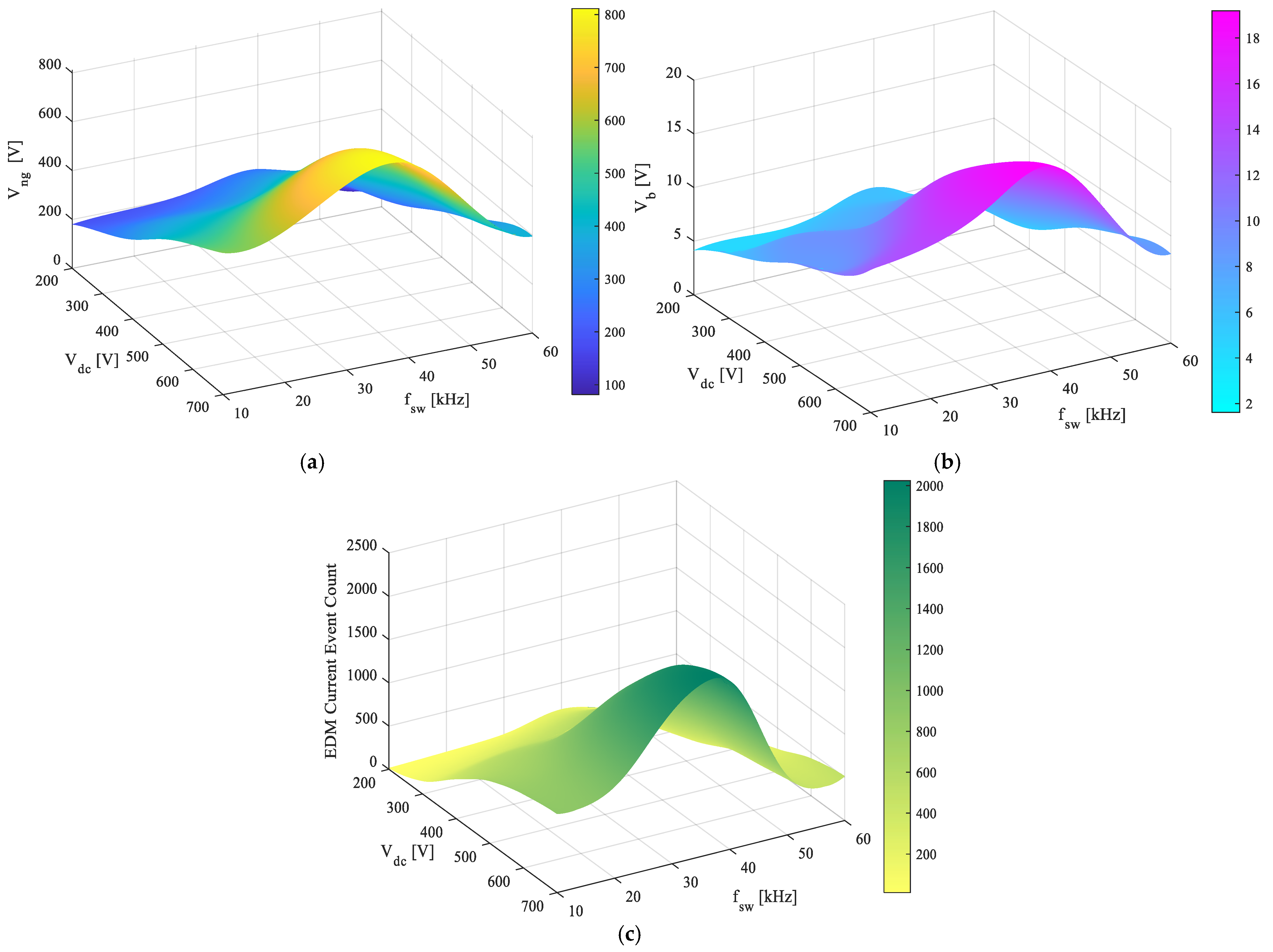
Figure 18 illustrates the combined effects of switching frequency and dc-link voltage on neutral point voltage, bearing voltage, and EDM event count. As shown, the neutral point voltage exhibits a nonlinear variation with switching frequency, attributed to its capacitive behavior, and a linear increase with dc-link voltage, owing to its dependence on the inverter CM voltage (see
Figure 18a). Since the bearing voltage and the corresponding EDM current event count depends on motor neutral point voltage, both follow a similar trend with switching frequency and dc-link voltage (see
Figure 18b,c), that is, with lower values of both observed at low switching frequencies and dc-link voltages. The values increase progressively and reach a maximum when the switching frequency equals the motor antiresonance frequency (i.e.,
= 40 kHz) at the highest applied voltage (i.e.,
= 700 V). Beyond this antiresonance frequency, a further increase in switching frequency results in a decrease in these values, although they remain comparatively high at elevated voltage levels.
5. Proposed CM Choke Design Approach
This paper employs a bearing voltage reduction approach to prevent EDM current events. As outlined in
Section 4, when the bearing voltage exceeds the breakdown voltage of the bearing lubricant, the lubricant insulation fails and allows the current to pass through the bearing, resulting in EDM current spikes. To eliminate these spikes, it is essential to reduce the bearing voltage below the lubricant breakdown voltage. As detailed in
Section 2, the bearing voltage is directly proportional to the motor neutral point voltage.
Therefore, reducing the neutral point voltage will inherently reduce the bearing voltage, which decreases the likelihood and magnitude of EDM current generation.
Since the practical switching frequency of IGBT inverters is limited to 20 kHz and motor antiresonance frequencies are typically higher than 40 kHz, the CM chokes conventionally designed for IGBT inverters typically operate under the condition of
, where
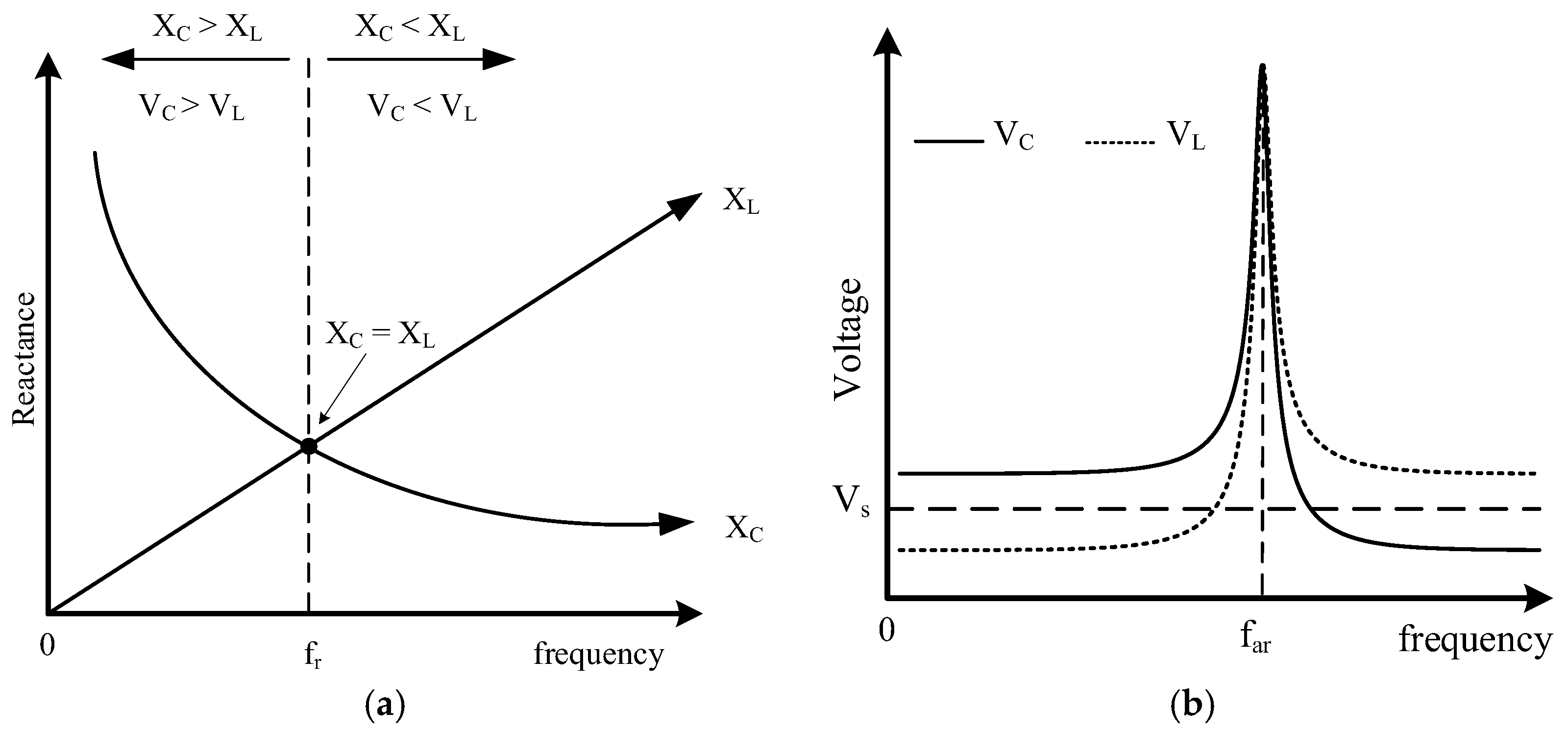
represents the motor antiresonance frequency shifted to lower values due to the inclusion of the CM choke. In this condition, motor neutral point voltage tends to be higher than inverter CM voltage (see
Figure 3a,b). Consequently, the conventional CM choke is ineffective at reducing the neutral point voltage and the corresponding bearing voltage. To effectively mitigate these voltages and, in turn, EDM current events, the shifted antiresonance frequency must be lower than the switching frequency, i.e.,
. Therefore, this paper proposes a CM choke design that optimally shifts the motor antiresonance frequency below the switching frequency, leading to negligible neutral point and bearing voltages, thereby eliminating the EDM bearing current spikes.
5.1. CM Choke Inductance Selection
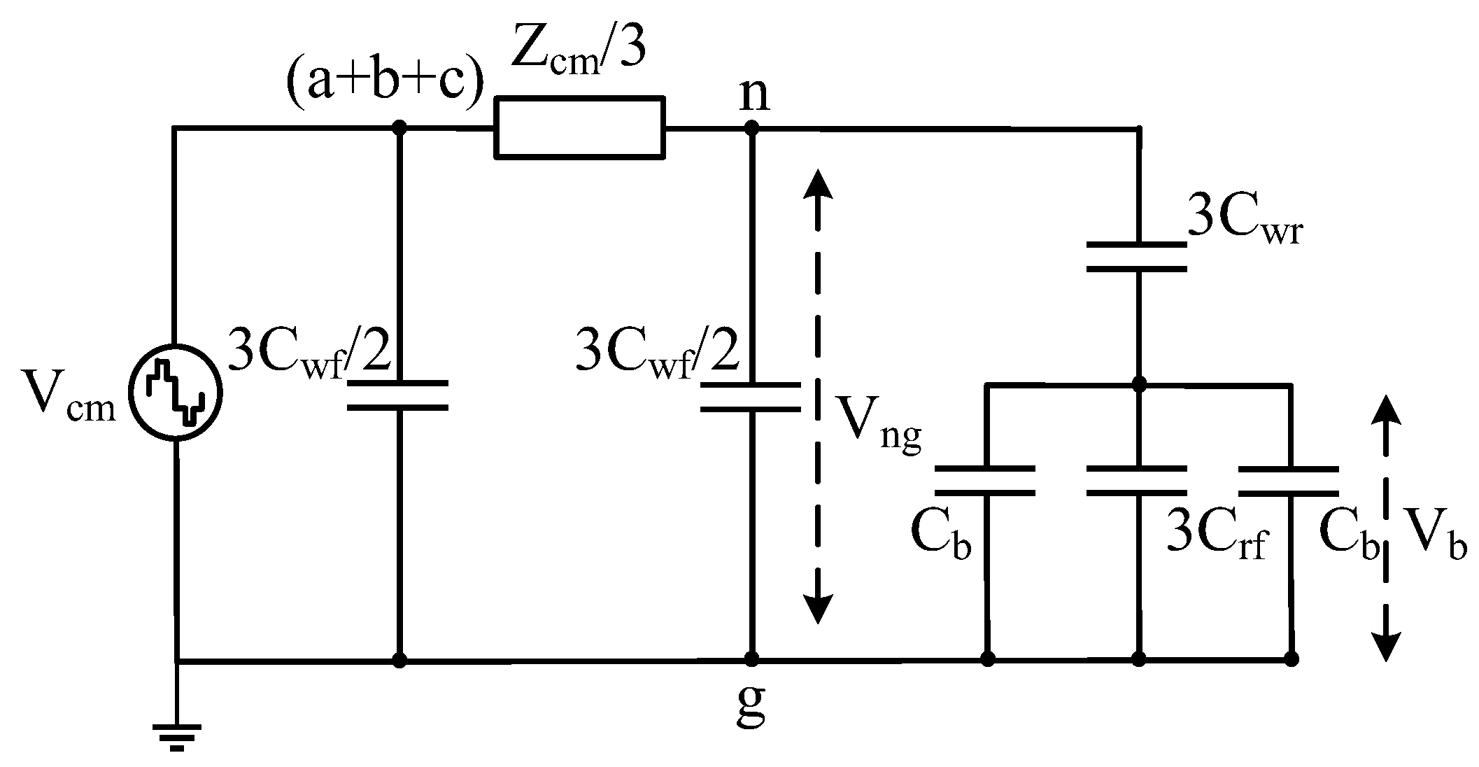
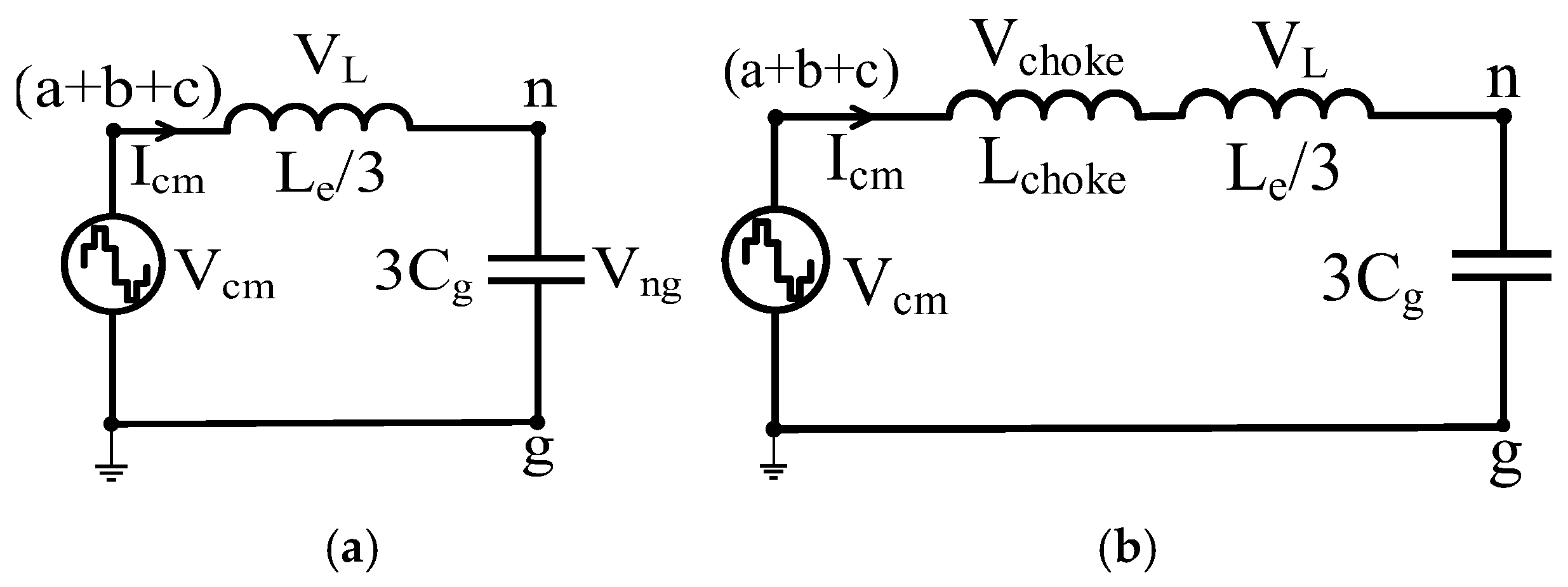
In this paper, CM choke inductance is determined based on the principle of shifting motor antiresonance frequency to a lower value relative to switching frequency. Referring to
Figure 2, the winding-to-frame capacitance is much higher than other parasitic capacitances; therefore, it acts as the dominant capacitance, and other capacitances can be neglected. As a result, the motor CM equivalent circuit shown in
Figure 2 can be simplified into a series LC circuit consisting of three-phase equivalent CM inductance
and equivalent capacitance between neutral point and grounded frame
(i.e.,
), as shown in
Figure 19a. According to
Figure 19a, the motor antiresonance frequency
is given by
By shifting
to a lower value than the switching frequency, the capacitive voltage of the motor CM equivalent circuit (i.e.,
) can be decreased. According to Equation (2), this can be achieved by increasing either
,
, or both. Due to the series connection of the CM choke with the motor, its inductance is added to the motor CM equivalent inductance, as shown in
Figure 19b. Hence, the total CM inductance increases, effectively shifting the motor antiresonance frequency to a lower value. According to
Figure 19b, the shifted antiresonance frequency
of the motor, influenced by the series addition of the CM choke inductance
, is
From Equations (2) and (3), the value of
can be calculated as
where per-phase winding inductance can be determined by rearranging Equation (2) as
Referring to
Figure 11, the antiresonance frequency of the utilized motor is observed as 41.6 kHz, whereas
can be calculated from the magnitude of CM impedance
in the low-frequency range (i.e., 1 kHz to 10 kHz), as
where
and
represent the selected frequency in the low-frequency range and the CM impedance value, respectively. By substituting the determined parameters in Equation (5), the value of
for the motor under test is determined as 10.8 mH.
From Equation (4), the value of CM choke inductance required to shift the motor antiresonance frequency to an arbitrary low value can be obtained. However, the optimum shift required in the antiresonance frequency to reduce the bearing voltage to a certain level and eliminate the EDM current spikes requires further calculations.
Motor neutral point can be calculated by applying a voltage divider rule on the CM choke-connected motor CM equivalent circuit shown in
Figure 16b. Since the CM choke is designed to reduce the motor antiresonance frequency below the switching frequency, the CM voltage as a function of inductive and capacitive voltage is given as
where (
). Using the voltage divider rule,
can be calculated as
Since the RMS value of CM voltage and the corresponding neutral point voltage varies inversely with the modulation index, the proposed approach is designed for the worst-case scenario where the modulation index is low (i.e., high
). In the case of lower modulation indices, the three phases switch almost simultaneously. As a result, the inverter CM voltage approximates a square wave, with its RMS value equal to its peak value. Therefore, Equation (8) can be rewritten in terms of peak values rather than RMS values, as
Rearranging Equation (9), the ratio of peak neutral point voltage and peak CM voltage is given by
Equation (10) indicates that the motor neutral point voltage can be reduced to any fraction
of the inverter CM voltage by adjusting the ratio of
and
. Substituting
and
into Equation (10) and the values of
from Equation (4) and
from Equation (2) afterwards, the ratio of the shifted antiresonance frequency and switching frequency can be expressed as
Incorporating Equation (11) into Equation (4), the CM choke inductance required to limit he neutral point voltage to any fraction
of the CM voltage is given by
Equation (12) provides the required choke inductance to reduce the peak neutral point voltage to any fraction “k” of the inverter CM voltage. To ensure the elimination of EDM current, the bearing voltage must be reduced below a critical threshold. Consequently, the value of “k” can be determined based on the required peak bearing voltage level.
From Equation (10), the peak neutral point voltage can be given as
The peak neutral point voltage can also be calculated using the BVR of the motor given in Equation (1) as
Equating Equations (13) and (14) yields
From Equation (15), the value of “k” can be calculated for any desired peak value of the bearing voltage. The “k” value directly impacts the choke core design and size, specifically the CM volt-seconds impressed on the choke core. The CM volt-seconds can be given as
where
is the switchinng period and
is the CM voltage drop across the CM choke, where the value of
can be determined by converting Equation (7) into peak values and substituting the value of
from Equation (13) afterwards, as
Assuming a negligible voltage drop across the motor CM winding to emulate the worst-case scenario, the entire CM voltage is dropped across the choke coil. Therefore,
, substituting the value
in Equation (16) and solving the integration yields
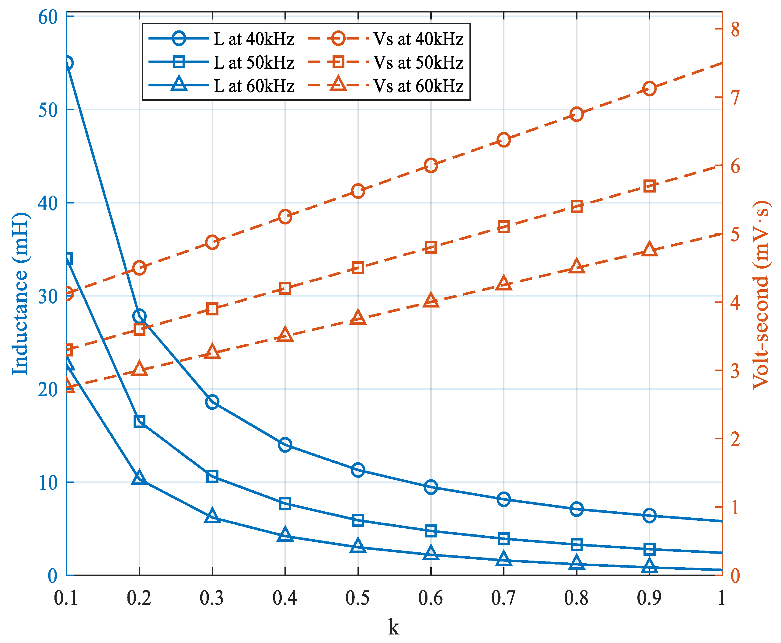
To analyze the impact of the fraction “k” on CM volt-seconds, different values of “k” ranging from 0.1 to 1 are substituted into Equation (18), considering switching frequencies of 40, 50, and 60 kHz and a constant dc-link voltage of 600 V. The corresponding CM choke inductances and volt-seconds experienced by the choke core for varying “k” values are shown in
Figure 20. As observed, both the required choke inductance and the core volt-seconds decrease as the switching frequency increases. Additionally, lower “k” values require larger choke inductances compared to higher “k” values; however, the volt-seconds across the core are reduced at lower “k” values. Since the volt-seconds are directly proportional to the maximum flux density
of the core, as expressed in Equation (19), higher “k” values may cause the choke core to saturate, leading to a loss of inductance capability.
where
is the number of turns and
is the effective cross-sectional area of the core.
Furthermore, at higher “k” values, the reduction in choke inductance corresponds to fewer turns, which again increases the maximum flux density and the risk of core saturation. Therefore, to ensure the practical feasibility of the choke size, the “k” value should be kept as low as possible. Although a higher choke inductance will be required at lower “k” values, the size of the choke will remain practical since the core volt-seconds will be lower.
For the motor under test, selecting a peak bearing voltage of 1 V to fully eliminate EDM currents results in a calculated “k” value of 0.15 using Equation (15), assuming a peak CM voltage of 300 V and the BVR of the motor as 2.2% (calculated based on the peak values of neutral point voltage and bearing voltage). Based on this “k” value, the required choke inductance at a switching frequency of 40 kHz is calculated as 37 mH using Equation (12).
5.2. CM Choke Core Selection
In this paper, the CM choke is designed to shift the motor antiresonance frequency below the switching frequency, resulting in nearly all the inverter CM voltage being dropped across the CM choke. Consequently, the primary concern is the core’s ability to withstand the source CM voltage for a period determined by switching frequency. Therefore, to select the appropriate CM choke core, it is important to first calculate the CM volt-seconds across it.
To ensure that the selected choke core is capable of withstanding maximum voltage stress, a worst-case operating condition is assumed. First, the CM voltage drop across the motor winding inductance is considered negligible (i.e., ≈ 0), such that the entire inductive CM voltage is imposed across the choke. Additionally, a low modulation index is assumed, representing a scenario in which an RMS CM voltage equal to its peak value (i.e., ) is continuously applied across the choke within a switching cycle. Under these assumptions, given a switching frequency of 40 kHz and dc-link voltage of 600 V, CM volt-seconds across the CM choke core can be calculated for k = 0.15 as Vs using Equation (18).
Furthermore, a nanocrystalline core material with a saturation flux density
of 1.2 T–1.3 T is selected. Therefore, the maximum flux density
in the core is selected to be less than 1.2 T. According to Equation (19), to prevent core saturation, the product of
and
must be greater than or equal to
. Therefore, by substituting the values for the maximum flux density and maximum volt-seconds into Equation (19), and considering the number of turns as 40, the cross-sectional area of the core should be larger than 0.89 cm
2. Furthermore, determining the inner and outer diameters of the core requires the calculation of the magnetic path length
, which can be derived from the CM choke inductance as
where
. For nanocrystalline materials, the relative permeability
is approximately 30,000, yielding a total permeability μ = 3.77 × 10
−2 H/m. Substituting the calculated values into Equation (20), the magnetic path length can be determined as 14.5 cm. Using the values of
and
and considering the height of the core as 20 mm (for practicality), the inner and outer diameters of the CM choke core are determined as 41 mm and 50 mm, respectively.
The calculated dimensions indicate that the CM choke can effectively withstand 115% of the inverter CM voltage at of 600 V and switching frequency matching machine antiresonance frequency, even at low modulation index. The resulting CM choke size is practical, and a suitable core can be readily selected from commercially available options.
In this paper, a nanocrystalline (Magnetec NANOPERM M-011, 50 × 40 × 20 mm
3) core is selected that achieves a volumetric power density of approximately 8–12 kW/L, which is within the same order of magnitude as advanced traction inverters that integrate planar EMI filters, where system-level power densities of 25–35 kW/L have been reported [
27,
28]. The high saturation flux density (≈1.3 T) and low-loss properties of the nanocrystalline material enable a 30–50% reduction in volume compared with ferrite equivalents while maintaining thermal stability and magnetic headroom. Although the material cost (≈USD 3–25 per core) is higher than that for ferrites, it is justified by the compactness, reliability, and EDM-current suppression that improve drivetrain durability. Therefore, the proposed CM choke offers a practical balance among performance, cost, and volume for WBG inverter-based applications.
5.3. Evaluation of Saturation Margin of the Selected CM Choke Core
The selected nanocrystalline core has a saturation flux density of 1.3 T. The proposed CM choke core is designed to tolerate up to 115% of the CM voltage, resulting in a maximum flux density of 1.18 T. This corresponds to a nominal saturation margin of approximately 9.23%. Although this margin appears narrow, it represents a highly conservative case established to capture worse-case operating conditions. Specifically, the flux density and volt-second stress are evaluated at an extremely low modulation index (≈0), where the CM voltage exhibits its highest magnitude. However, such low modulation indices are not encountered during normal inverter operation.
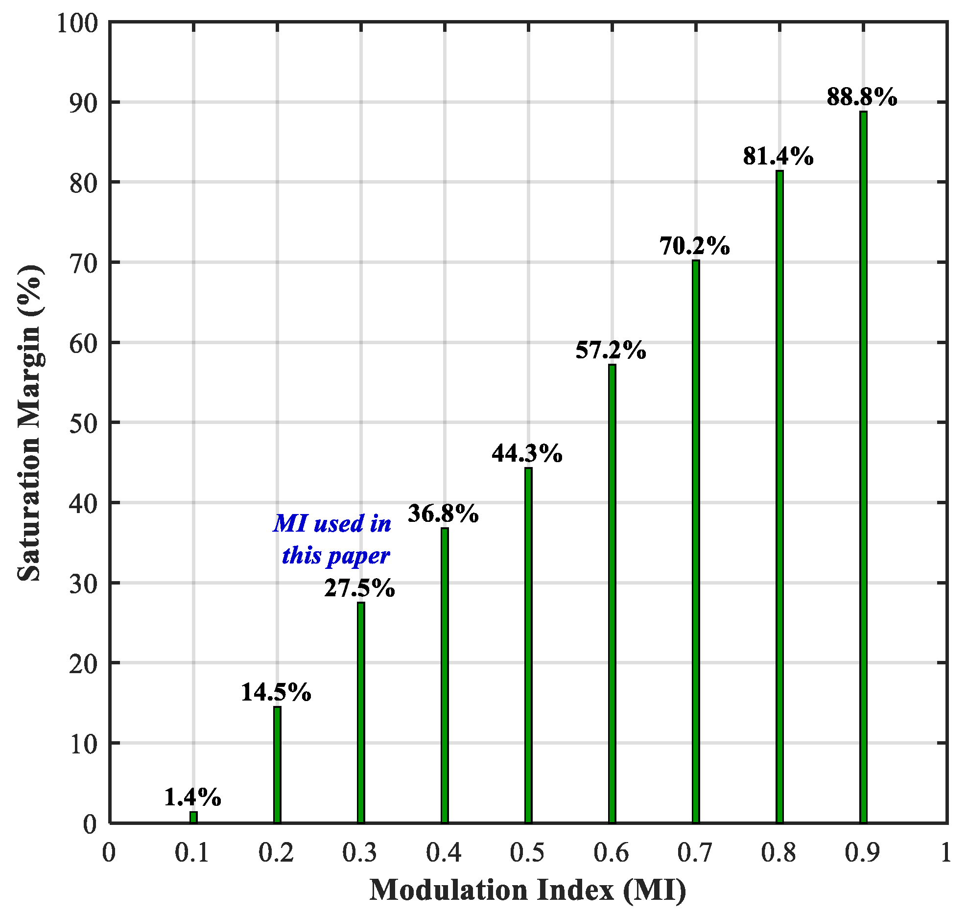
In practical operation, as the modulation index (MI) increases, the CM voltage transitions from a bipolar square wave to a quasi-square shape; therefore, its effective RMS value decreases, leading to a lower flux swing and greater magnetic headroom. Since no explicit analytical relationship between modulation index and CM voltage RMS is available in the literature, a rough estimation is obtained using MATLAB/Simulink R2022b for a two-level VSI ( = 600 V, = 40 kHz). The simulated CM voltage RMS values for modulation indices from 0.1 to 0.9 are then used to compute the corresponding flux linkage (λ), core flux density (), and saturation margins relative to the nanocrystalline core’s saturation flux density.
To emulate transient and surge conditions, a +20% increase in dc-link voltage is applied in all calculations, and the resulting margins are presented in
Figure 21. The results indicate that the lowest margin occurs near MI = 0.1, where
≈ 1.28 T (≈1.4% margin). At MI = 0.3, which is the operating point used in this paper, the saturation margin is approximately 27.5%, even with the 20% surge and 1.15 × V
cm stress considered. The margin increases progressively with modulation index, exceeding 80% at M = 0.9.
These results confirm that the choke remains well below the saturation limit under both nominal and transient high-voltage conditions. The corner-case evaluation thus validates that the design is conservative and possesses sufficient magnetic headroom for all expected inverter operating scenarios.
6. Experimental Validation
Experimental analysis is carried out on a 2.2 kW three-phase four-pole star-connected induction motor supplied by a three-phase SiC two-level VSI, as shown in the experimental setup in
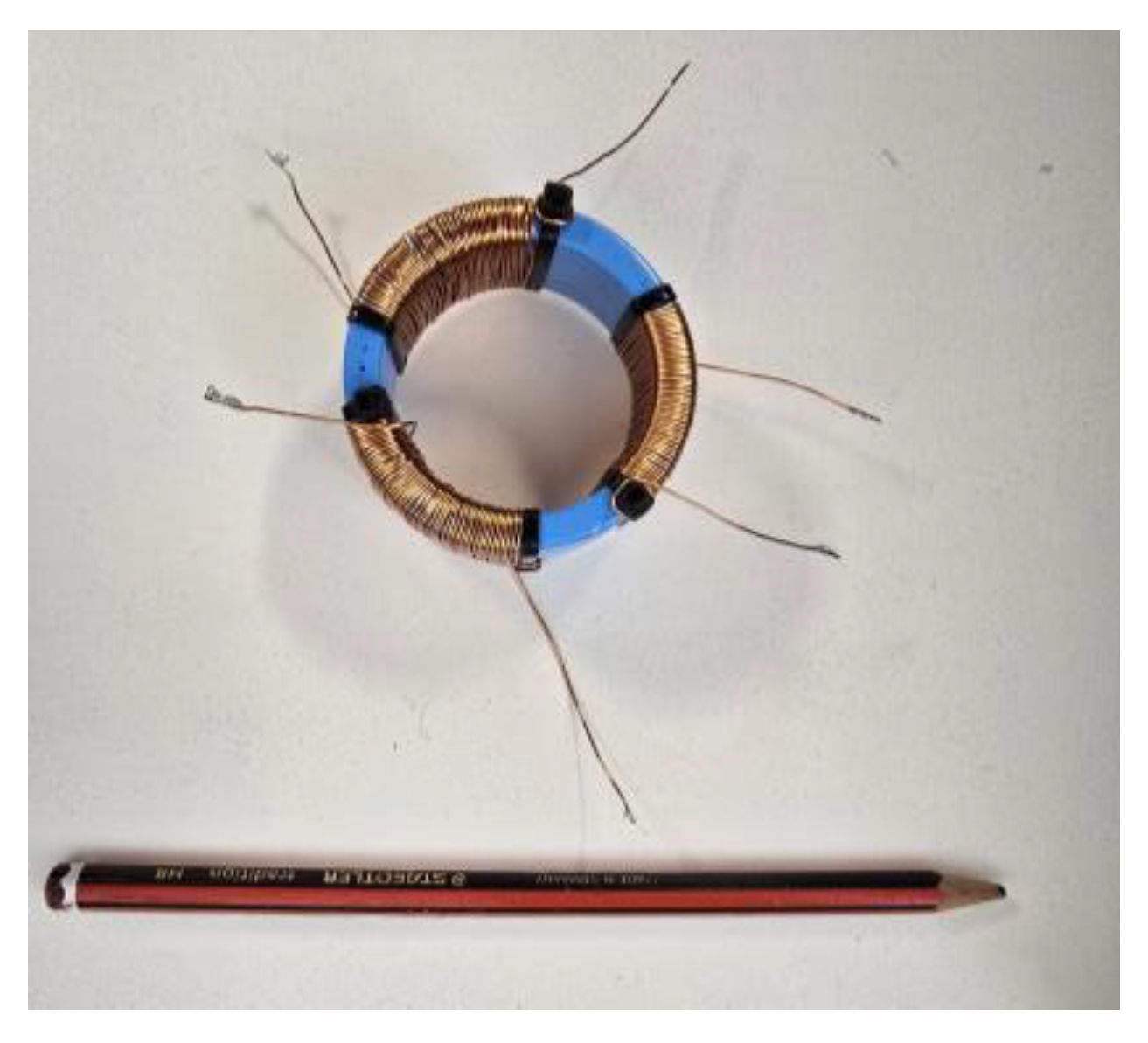
Figure 8. The designed choke and the selected choke core parameters used in the experiment are shown in
Figure 22 and
Table 3, respectively. The inverter is supplied with a constant dc-link voltage of 600 V at a modulation index of 0.3 and switching frequency of 40 kHz.
6.1. Impact of Proposed CM Choke Connection on Motor Bearing Voltage
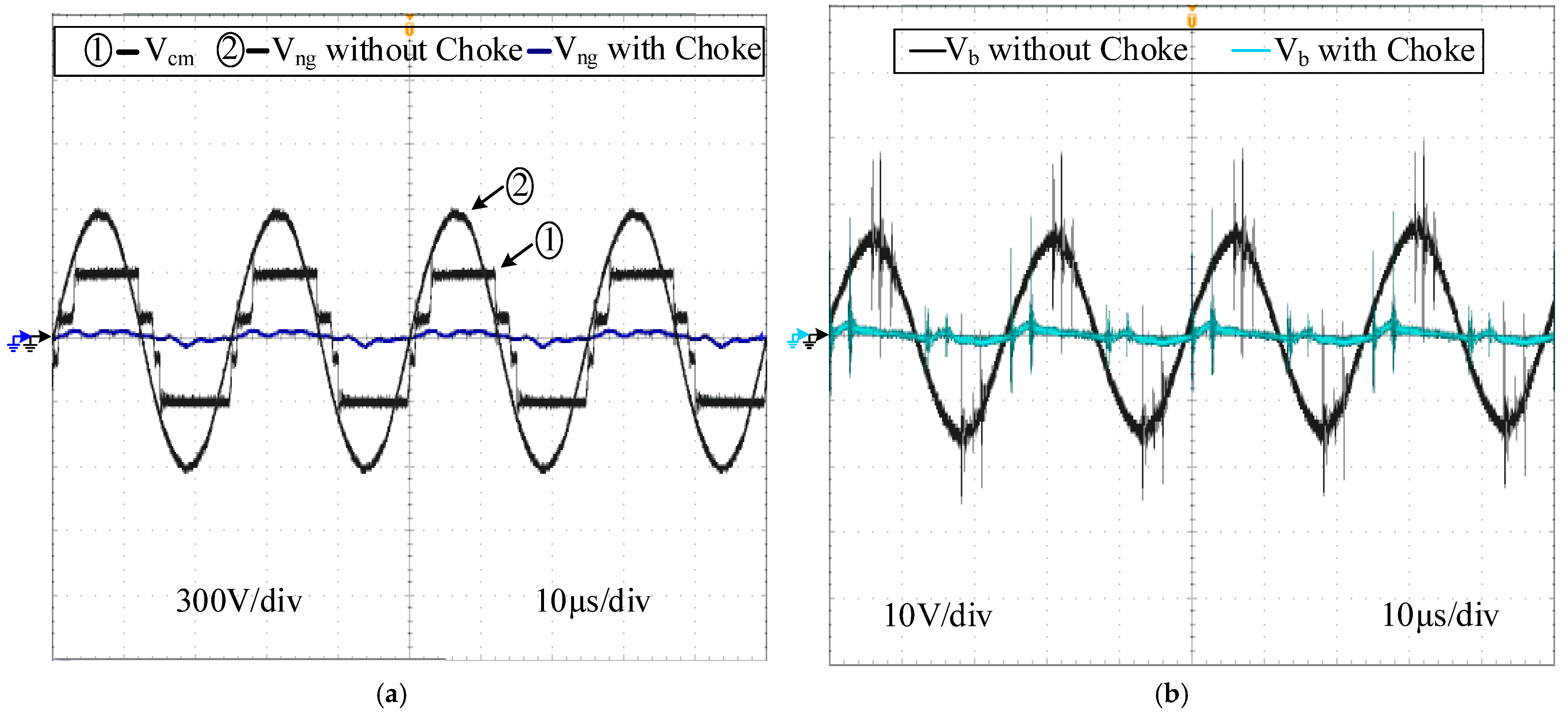
To evaluate the effectiveness of the proposed CM choke in mitigating motor neutral point voltage and resulting bearing voltage, measurements are conducted for both voltages with and without the proposed CM choke connection. On the other hand, the CM voltage is calculated by averaging the inverter pole voltages.
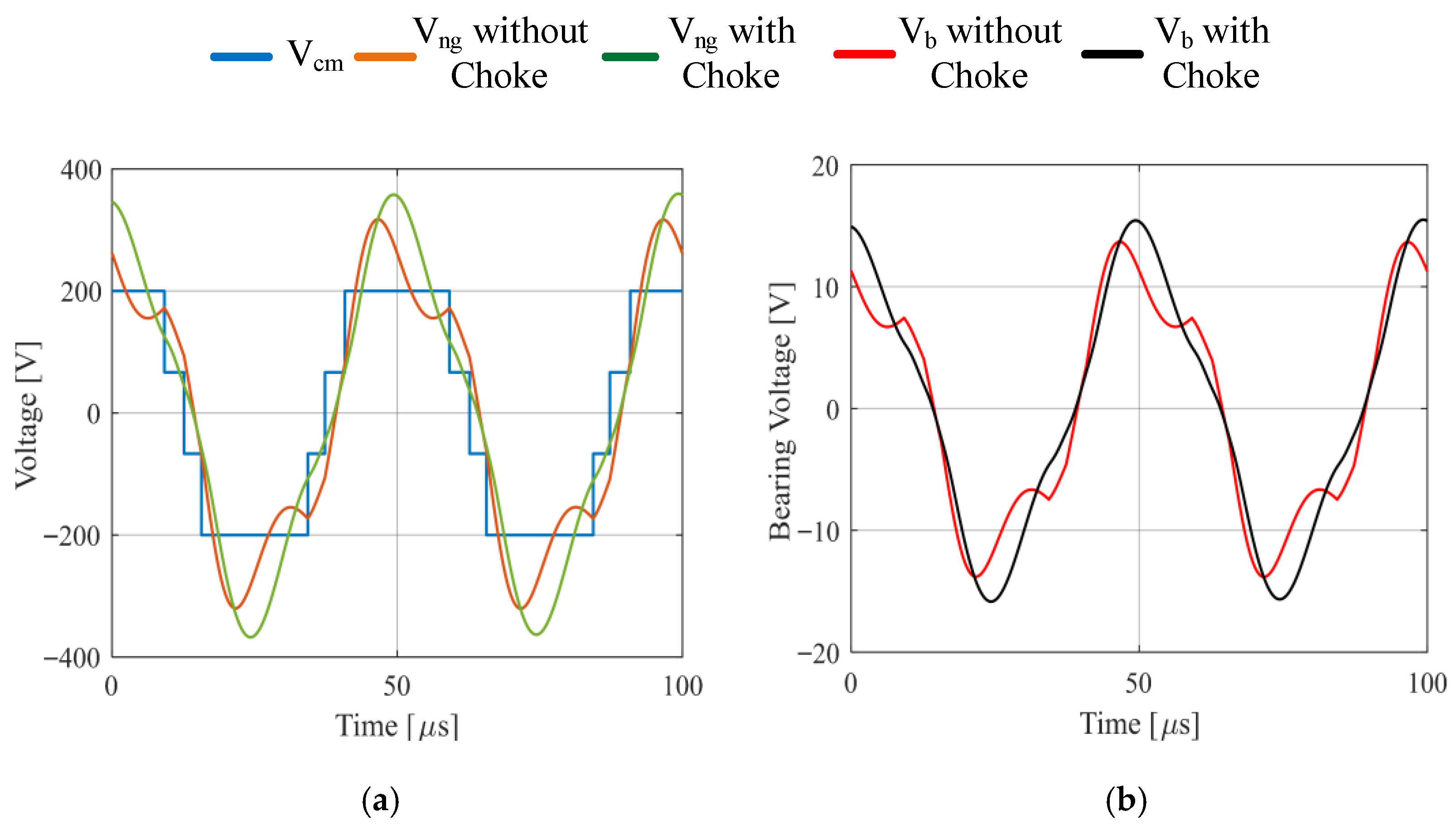
Figure 23 shows the results obtained. As shown, without the CM choke connection, the peak amplitude of the neutral point voltage
reaches 600 V (i.e., 2 pu) (
Figure 23a), while the peak bearing voltage is observed as 17 V (
Figure 23b). Such a high motor neutral point voltage and bearing voltage pose a significant risk to motor winding insulation and bearings. However, with the implementation of the proposed CM choke, the peak neutral point voltage drops to 35 V (i.e., 0.12pu), and the peak bearing voltage drops to 1 V. This substantial reduction in motor neutral point and bearing voltage minimizes electrical stress on motor windings and effectively suppresses the risk of EDM-induced damage to bearings.
6.2. Impact of Proposed CM Choke Connection on EDM Bearing Current
In the case of motor drive operation without any CM choke connected, the highest EDM current count occurred when the switching frequency matched the machine antiresonance frequency, particularly under the high dc-link voltage condition (i.e., at 40 kHz and 600 V) (see
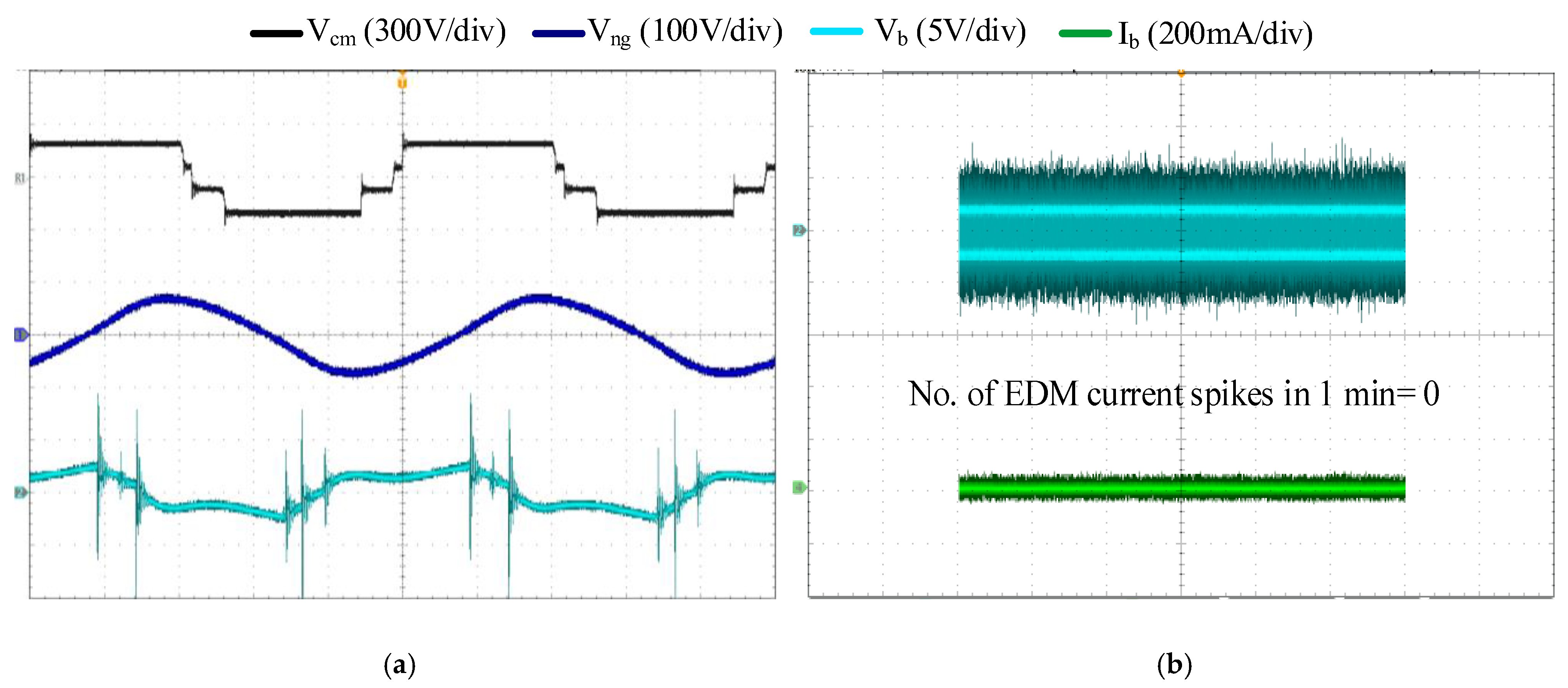
Figure 16d). To validate the effectiveness of the proposed approach under these conditions, the bearing current is measured at a switching frequency of 40 kHz, dc-link voltage of 600 V, and modulation index of 0.3 with connection of the proposed CM choke. The experimental results, presented in
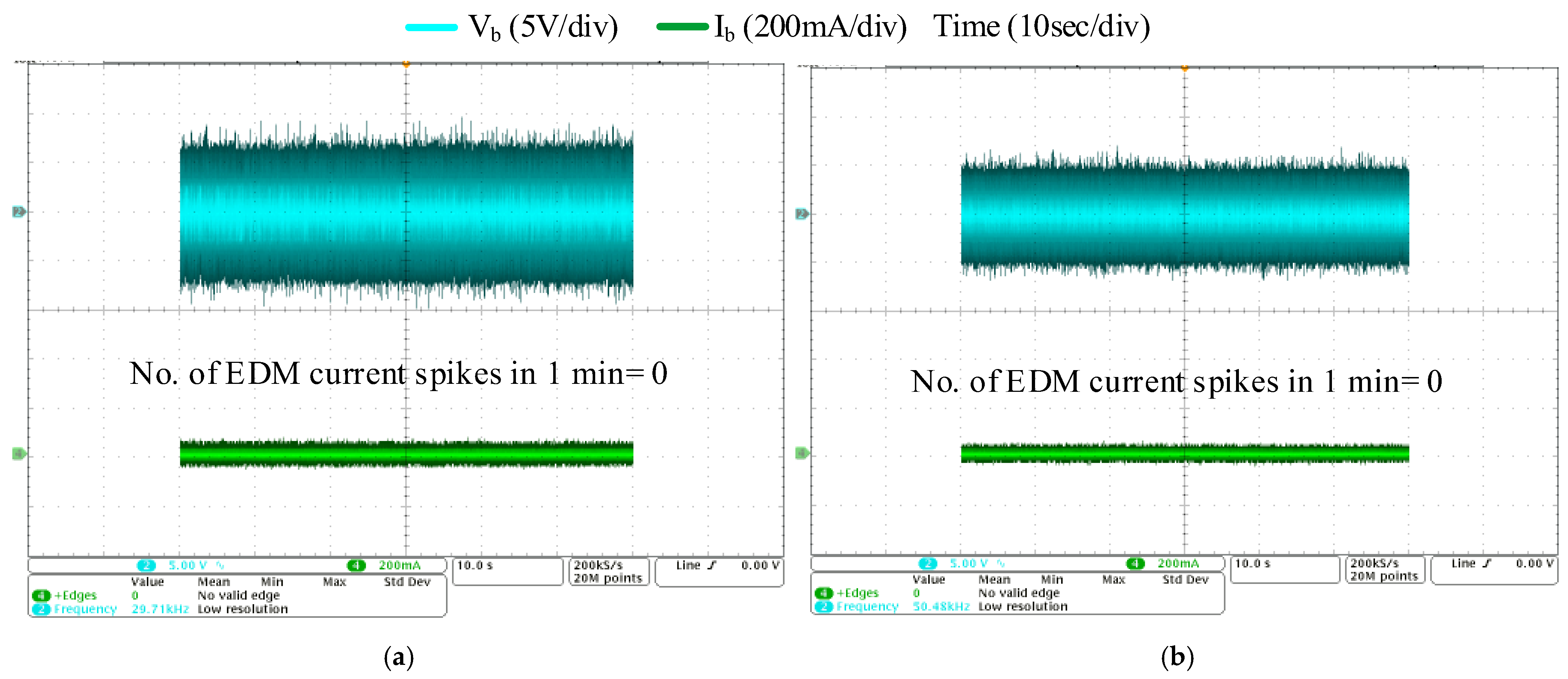
Figure 24a, show a complete elimination of EDM current spikes over the specified time frame, whereas 1887 EDM current spikes were recorded in the same time frame when no mitigation was considered.
To further validate the performance of the proposed CM choke, the bearing current is monitored over an extended duration of 10 min, as shown in
Figure 24b. It is observed that, with the proposed CM choke connected, no EDM current spikes > 100 mA occur even over the prolonged observation period.
6.3. Impact of Proposed CM Choke Connection on Motor Common-Mode and Line Current
To analyze and compare the CM current of the motor drive system with and without the proposed CM choke connection, measurements are taken using a current probe placed across the three lines of the motor (AC side) and around both positive and negative DC buses (DC side). The proposed CM choke lowers the motor’s antiresonance frequency relative to the switching frequency, thereby reducing the neutral point voltage, bearing voltage, and the associated EDM bearing current. As the neutral point voltage is the primary driver of CM current, this reduction decreases CM current flow from the motor winding-to-frame/ground (AC side). The CM current, however, circulates in a closed loop: Inverter → Motor windings/parasitics → Motor frame → Ground → DC source/AC mains → Inverter. Hence, any reduction on the AC side inherently leads to a corresponding reduction on the DC side. Thus, the implementation of the CM choke provides simultaneous suppression of CM current on both sides of the inverter.
The results, presented in
Figure 25a, show the CM current measured simultaneously on the AC and DC side of the inverter without the CM choke. As shown, the CM current is similar in magnitude as well as waveshape on both sides of the inverter. Furthermore, without the CM choke, CM current exhibits a sinusoidal waveform with high-frequency harmonics and a peak amplitude of 0.9 A, primarily due to the high neutral point voltage. However, with the optimally designed CM choke in place, the CM current is reduced by 83%, lowering the peak amplitude to 0.15 A while also minimizing harmonic content, as shown in
Figure 25b.
Figure 25c presents the frequency spectrum of the CM current. Notably, with the proposed CM choke, the overall CM current harmonics are attenuated as compared to the case of without the CM choke. Furthermore, in the higher frequency range (i.e., 10 MHz onwards), it remains around 50 dBµA. Although the proposed choke is designed to eliminate the EDM bearing current, it also attenuates the AC and DC side CM current peak and CM-EMI by reducing the neutral point voltage.
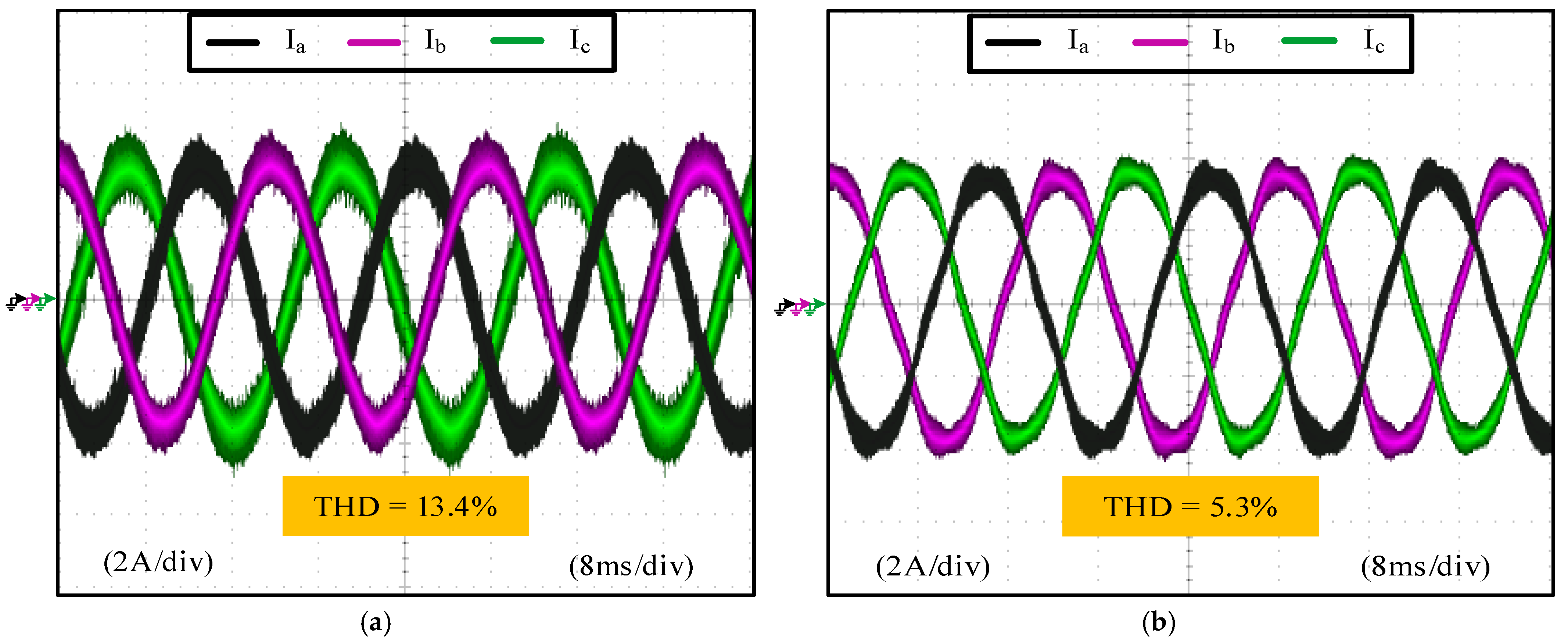
The line currents also benefit from the proposed CM choke connection, as shown in
Figure 26. Without the CM choke, line currents show a peak of approximately 4 A with a noticeable ripple. With the proposed CM choke installed, the peak line current remains almost the same; however, the ripple amplitude is effectively reduced, resulting in a smoother sinusoidal waveform with total harmonic distortion reduced from 13.4% to 5.3%. This demonstrates that the proposed CM choke not only suppresses CM disturbances on both the AC and DC sides but also improves line current quality, enhancing overall system performance.
Table 4 summarizes the measured impact of the proposed approach on motor parameters in the worst-case scenario. Significant reductions are achieved across all metrics, including a 94% decrease in peak bearing voltage, complete elimination of EDM current spikes, and an 83% reduction in peak CM current. The average EMI level is also lowered from approximately 85 dBµA to 75 dBµA, indicating improved compliance with EMC guidelines and reduced stress on motor bearings.
6.4. Robustness of the Proposed CM Choke Design Under Parasitic Element Variations
The accuracy of parasitic parameter estimation can be influenced by insulation aging, temperature, and variations among motor designs. Published studies report measured trends in stator insulation capacitance and winding inductance under these conditions, although explicit absolute percentage changes are limited. For example, the Electric Power Research Institute (EPRI) report on thermal aging of stator windings shows that winding-to-frame capacitance changes are typically below 2–3% under moderate deterioration [
29]. Thermal-aging experiments on enameled coils indicate similar gradual increases with aging [
30], while dielectric measurements on traction-motor winding insulation under thermal aging show a ±1–5% change, with typical operating temperature variations [
31]. For the magnetic components, manufacturer data show that permeability variations with temperature can lead to inductance changes of up to ±30%, with typical production tolerances of ±10–20% [
32].
Based on these reported trends, a winding-to-frame capacitance variation of up to ±30% and a common-mode winding inductance variation of ±50% is considered for robustness analysis.
Figure 27 shows the variation in bearing voltage with the variation in motor parasitic element values. These bearing voltage values are obtained when a fixed proposed CM choke of 37 mH is connected for the worst case of 600 V dc-link voltage and 40 kHz switching frequency. Using the design Equation (12), the “k” values are calculated for each parameter variation and then substituted in Equation (15) to estimate the bearing voltages. As observed in the chart, even with the widest ranges of parameter variations, the peak bearing voltage consistently remains below 3 V, and EDM spikes are unlikely at this small bearing voltage.
To further validate this claim, the motor operating points are adjusted such that, with the proposed 37 mH CM choke, the resulting bearing voltage reaches approximately 3 V (to emulate parameter variation). Under operating conditions of 25 kHz switching frequency, 400 V dc-link voltage, and a modulation index of 0.3, the measured bearing voltage is approximately 3 V, as shown in
Figure 28a.
Figure 28b shows the corresponding EDM bearing current. As seen, there are no EDM spikes observed even when the bearing voltage increases to 3 V. This confirms that the proposed CM choke design remains resilient to both manufacturing tolerances and operational variability.
6.5. Robustness of the Proposed CM Choke Design Across Different Operating Conditions
To confirm the robustness of the proposed 37 mH CM choke (designed for switching frequency of 40 kHz) across different converter operating points, additional evaluations are conducted using switching frequencies of 30 kHz and 50 kHz, while all other parameters remain constant. Since the CM voltage, neutral point, and the resulting bearing voltage scale with the dc-link voltage, a lower dc-link voltage inherently reduces these voltages. Therefore, the robustness assessment is carried out at the highest test dc-link voltage of 600 V to represent the most severe operating condition.
The proposed CM choke is analyzed using the design Equation (12) to compute the “k” value for each switching frequency while keeping fixed at 37 mH. The calculated “k” values of 0.29 and 0.09 for 30 kHz and 50 kHz, respectively, are used to estimate the bearing voltage from Equation (15) and the λ using Equation (18). With a worst-case CM voltage of 300 V and a BVR of 0.022, the resulting bearing voltages are 1.9 V and 0.6 V for 30 kHz and 50 kHz, respectively, while λ varies inversely, being 6.4 mVs at 30 kHz and 3.1 mVs at 50 kHz. Although λ increases slightly at the lower switching frequency, the experimental modulation index of 0.3 reduces the effective CM voltage below 300 V, which compensates for the rise in λ and ensures that both flux and remain within the non-saturating limits of the core.
Figure 29 presents the waveforms of the bearing voltage and EDM current measured at different switching frequencies. As shown, across all operating points, no EDM-related discharge spikes occur because the calculated bearing voltage remains below 2 V. These results demonstrate that the proposed single 37 mH CM choke, optimally designed for a switching frequency 40 kHz, exhibits strong robustness across different switching frequencies (higher and lower than 40 kHz). Even under high dc-link voltage, the magnetic stress and bearing voltage remain within safe limits, and no EDM discharge events are observed. Consequently, a single fixed-value CM choke can be confidently applied across a broad operating range, simplifying practical implementation in motor-drive systems.
6.6. Core-Loss Estimation and Thermal Validation of the Proposed CM Choke
This section presents the analytical estimation and experimental validation of core losses and thermal behavior for the nanocrystalline core employed in the proposed CM choke. The evaluation of the loss characteristics of the Magnetec NANOPERM M-011 material under high-frequency excitation and confirmation the thermal stability of the design under worst-case operating conditions are performed.
The nanocrystalline toroidal core used for the proposed CM choke (Magnetec NANOPERM M-011) is analyzed for core loss and thermal performance under high-frequency excitation. Core losses are estimated using the improved Generalized Steinmetz Equation (iGSE), which accounts for non-sinusoidal flux excitation. Based on the manufacturer’s material constants (k = 2.0 × 10⁻³, α = 1.45, and β = 1.95) at 100 °C, the equivalent coefficient kᵢ is derived and applied to evaluate the volumetric power loss.
For the applied ±300 V CM voltage (square wave) at 40 kHz and 44 turns per phase, the iGSE model predicts a total core loss of approximately 2.5 W, increasing to 4.9 W at 60 kHz for a flux swing of 2.4
. Thermal analysis based on natural convection (h = 10–20
) and the toroid surface area yielded a steady-state temperature rise of 24–48 K, corresponding to a core temperature of 44–68 °C at 40 kHz in a 20 °C ambient environment.
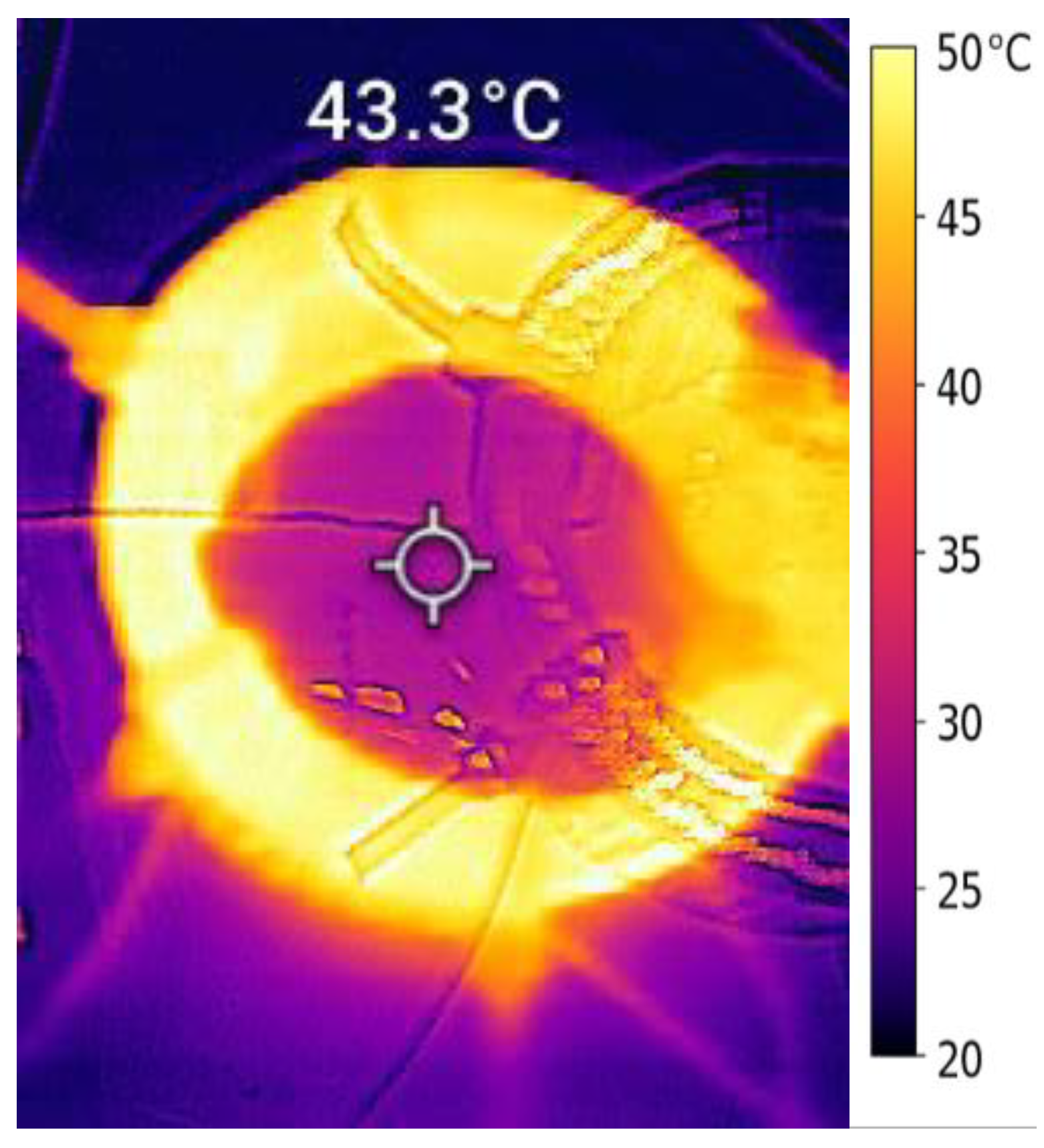
Figure 30 shows the experimental infrared thermography under
= 600 V and
= 40 kHz with a stabilized surface temperature of about 43.3 °C, indicating a loss of 1.2–2.3 W, which is less than the predicted value due to the reduced effective CM voltage (i.e., modulation index of 0.3) used during testing. Overall, the analytical and experimental results confirm low loss levels and thermally stable operation well below the 130 °C limit of the nanocrystalline material. All detailed calculation steps are provided in
Appendix A.
6.7. Experimental Evaluation of Proposed CM Choke Design Against Existing CM Voltage Reduction Methods for EDM Current Elimination
Several active CM voltage reduction methods have been proposed in the literature, as discussed in
Section 1. While each method employs a different technique, they all share a common limitation in that the maximum achievable CM voltage reduction is constrained to
. This reduced CM voltage is typically sufficient to eliminate EDM spikes at low switching frequencies. However, WBG inverters enable motor drives to operate at higher switching frequencies, increasing the possibility of switching frequency approaching the machine antiresonance frequency. This can excite machine resonance, resulting in a significant overvoltage at the machine neutral point. As the bearing voltage is directly proportional to the neutral point voltage, it can also increase and exceed the bearing lubrication breakdown threshold, even with the CM voltage being reduced to
. As a result, EDM current spikes can still be observed with reduced CM voltage approaches.
Among the CM voltage reduction methods, the modified PWM schemes, such as the AZSPWM, stand out as the most cost-effective solution. Therefore, the proposed approach is compared with the AZSPWM method to evaluate its effectiveness in eliminating EDM current spikes. For comparison, the motor drive under test is operated under the same proposed approach, effectively eliminating EDM current spikes at all switching frequencies. In contrast, under the AZSPWM1 operating conditions using the AZSPWM1 modulation technique instead of SPWM, measurements are recorded for the inverter CM voltage, motor neutral point voltage, bearing voltage, and bearing current.
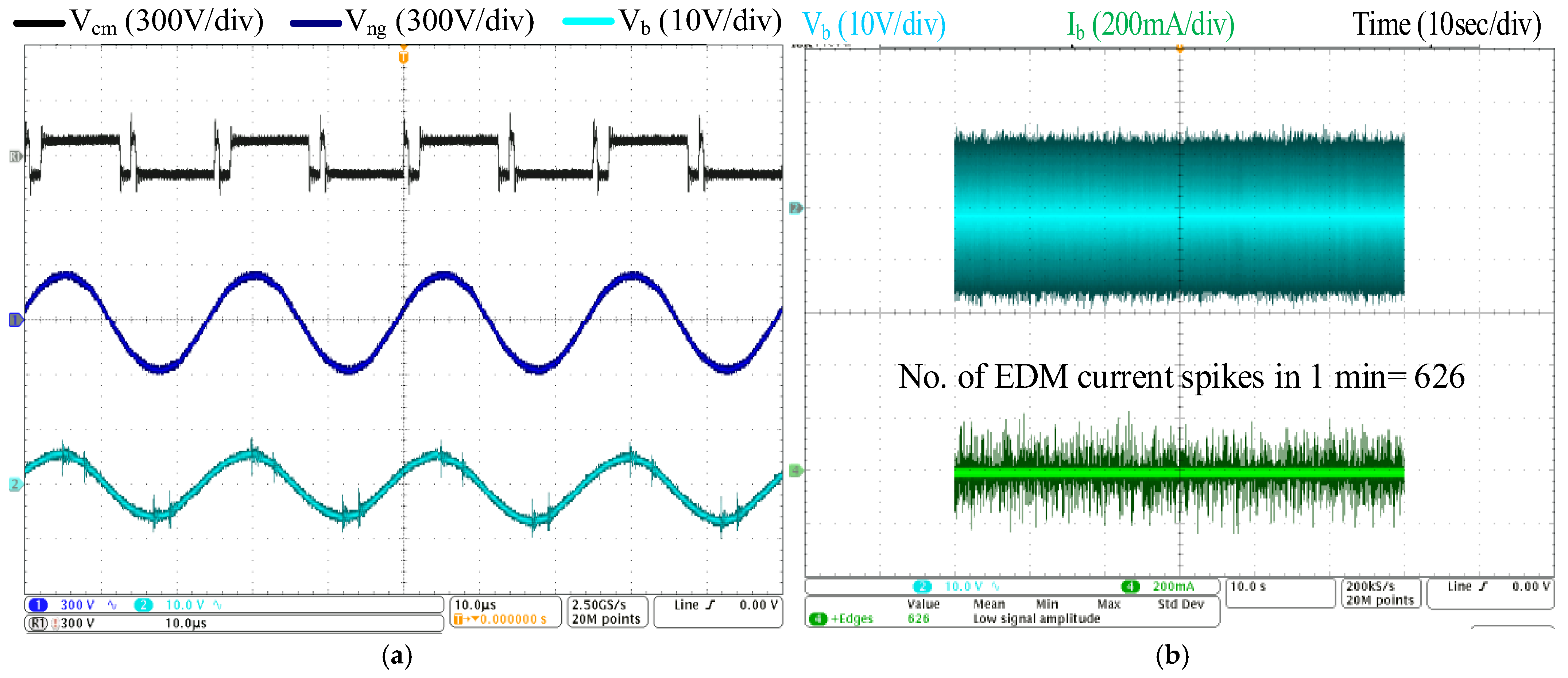
Figure 31 shows the experimental results under the AZPWM1 modulation method conducted at a dc-link voltage of 600 V and switching frequency of 40 kHz, while the modulation index is fixed at 0.3. From
Figure 31a, it can be observed that the peak CM voltage is limited to
100 V (i.e.,
). However, despite this reduction, a peak neutral point voltage of 290 V and a corresponding peak bearing voltage of 7 V can be observed. This bearing voltage is sufficiently high, exceeding the lubrication breakdown threshold, causing EDM current spikes (see
Figure 31b). As seen, there are 626 EDM current spikes occurring within a 1 min interval, which indicates persistent electrical stress on the motor bearing system. In contrast, the proposed approach demonstrates a complete elimination of EDM current spikes under identical operating conditions, as illustrated in
Figure 24.
