Article

A Graphical Tool for Predicting Class EF Inverter Behavior Including Non-Ideal Load Conditions

Universite Claude Bernard Lyon 1, Ampère, UMR5005, INSA Lyon, Ecole Centrale de Lyon, CNRS, F-69100 Villeurbanne, France
*
Author to whom correspondence should be addressed.
Energies 2025, 18(20), 5409; https://doi.org/10.3390/en18205409
Submission received: 17 September 2025 / Revised: 4 October 2025 / Accepted: 8 October 2025 / Published: 14 October 2025
(This article belongs to the Special Issue New Power System Planning and Scheduling)

Abstract

This paper presents a novel analytical framework for the design and understanding of class EF inverters under both optimal and non-optimal load conditions. Unlike conventional approaches that rely heavily on numerical simulations, the proposed method provides a fast, visual, and intuitive tool for analyzing inverter operation. Its effectiveness is demonstrated experimentally on a 15 MHz class EF inverter across three distinct load conditions, showing good agreement with theoretical predictions. To highlight the robustness and broad applicability of the approach, a class Φ 2 inverter—a lumped-element analog of the class EF inverter—is also implemented and successfully analyzed. By combining theoretical insight, experimental validation, and generalization to alternative topologies, the proposed framework offers an efficient, accessible, and versatile tool for high-frequency resonant inverter design.

1. Introduction

1.1. Generalities

Very-high-frequency (VHF) power converters have been extensively studied in recent years [1,2,3]. In comparison to conventional topologies, VHF power converters mitigate switching losses through the use of soft switching techniques, thereby significantly increasing the switching frequency to the tens of megahertz range. With a considerably reduced energy storage requirement, VHF techniques present substantial potential for enhanced power density and improved dynamic performance [3]. Among various VHF topologies, the class EF inverter employing a quarter-wave transmission line at the input of the circuit [4,5,6] is of particular interest (Figure 1a). This is especially true when the bulky transmission line is replaced with discrete reactive elements, resulting in what is referred to as a class Φ 2 inverter [7], as shown in Figure 1b. Today, this inverter topology is commonly used in VHF DC/DC power conversion applications [8,9,10] as well as in Wireless Power Transmission (WPT) systems [11,12,13]. Indeed, the relatively low voltage stress imposed to the switch compared to the class E inverter [14,15,16], combined with zero voltage switching (ZVS) and zero derivative voltage switching (ZdVS or ZDS) operations and simple driving requirements, makes this topology well-suited for high-power and high-frequency operations.

1.2. Challenges in Analytical Modeling and State of the Art

Although soft-switching class EF inverters and their lumped-element derivatives offer significant advantages, their development remains challenging, particularly when constructing accurate and structured models for systems with multiple resonant interactions. As rigorously detailed in [17], the analytical modeling of class EF inverter suffers from several major limitations.
First, an inherent trade-off exists between the complexity of the developed analytical model and its accuracy. Formulating the equations for the circuit depicted in Figure 1b requires handling a large number of interdependent variables [18,19,20,21]. High-order multivariable equation systems are difficult to solve analytically, and even numerical methods often struggle due to either excessive computation times [22] or challenges in determining suitable initial conditions that ensure algorithm convergence. To reduce the complexity of the resulting analytical model, it is common practice to neglect higher-order harmonics [23,24,25], which significantly impacts the accuracy of the developed model. Furthermore, some studies have proposed cascading resolution methods [26] aimed at gradually increasing the model complexity, thereby providing an adaptive, scalable framework tailored to specific accuracy requirements. Second, achieving ZVS and/or ZdVS operation introduces additional constraints. For instance, it is common to fix the duty ratio to a predefined value [19,20,27,28,29]. The resulting numerical solution, obtained under such constraints, does not represent the full set of achievable operating points. Investigating ZVS and/or ZdVS designs with novel characteristics thus requires repeating the entire analytical modeling process while applying constraints specific to the new operating conditions.
Today, the most common approaches for sizing the class EF inverter and its derivatives are the following:
  • Iterative circuit simulation, where parameters are manually tuned until a satisfactory operating point is found. This can take several days, depending on the designer’s experience [30,31].
  • Numerical resolution of time-domain equations, which is computationally heavy due to the high order of the circuit [18,19,20,21].
  • Machine learning models, trained on circuit simulation data to predict suitable operating points [17,22] or based on genetic algorithms [32].
In any case, to the best of our knowledge, there is currently no simple, systematic, and accurate design methodology that is both transparent and accounts for the specific soft-switching conditions of the class EF inverter and its lumped-element equivalents. Consequently, the development of complex topologies based on this specific inverter is severely hindered, significantly limiting the spread of HF/VHF power conversion through the field of power electronics.

1.3. Contribution of This Work

This paper introduces a comprehensive, systematic, and generalizable methodology for analytical design of class EF inverters and their lumped-element derivatives. Unlike iterative simulations or ML-based approaches, the proposed method provides closed-form equations and a practical design chart valid for any load condition.
The main contributions are the following:
  • Comprehensive analytical modeling: time-domain and harmonic analysis of the class EF inverter with a quarter-wave transmission line, capturing nonlinear voltage and current dynamics under arbitrary loads.
  • Practical design tool: a graphical design chart enabling rapid sizing and optimization without iterative simulations.
  • Experimental validation: measurements with a 15 MHz, 25 VDC class EF inverter confirm close agreement between theory and practice.
  • Applicability to lumped-element derivatives: the methodology is validated on the class Φ 2 inverter, showing its generality to discrete-element analogs of the class EF topology.

1.4. Paper Organization

The paper is organized as follows:
  • Section 2 introduces the comprehensive analytical modeling of the class EF inverter and presents two sizing equations derived from combined time-domain and frequency-domain approaches.
  • Section 3 applies constraints for ZVS and ZdVS operation, resulting in a set of nonlinear equations describing inverter behavior under soft-switching conditions. These equations are then gathered in a single user-friendly design chart, enabling fast and visual sizing of the class EF inverter for any load conditions.
  • Section 4 presents the experimental validation, first using a quarter-wave transmission line and then substituting it with discrete elements, confirming that waveform fidelity is maintained and demonstrating applicability to lumped-element equivalents (including class Φ 2 ).
  • Section 5 concludes the paper and discusses future perspectives in high-frequency power electronics.

2. Generalized Equations of Class EF Inverter

2.1. Starting Assumptions and Theoretical Background

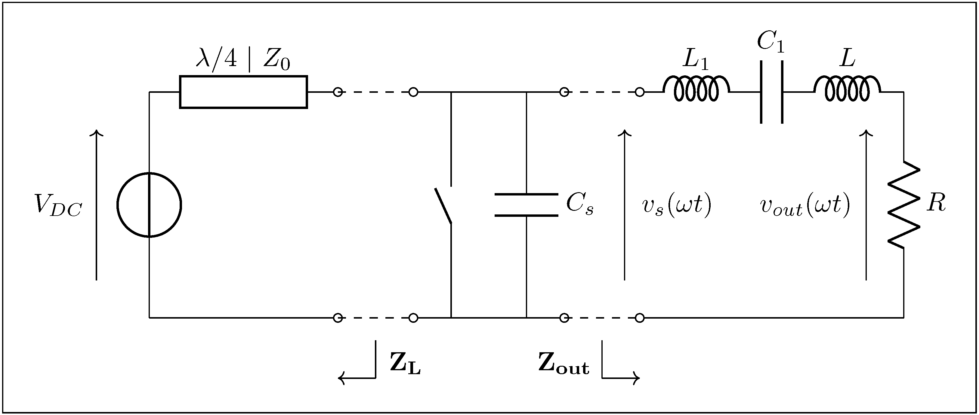
The basic form of the class EF inverter is depicted on Figure 2, it is composed of five main elements:
  • A single switch whose source is connected to the ground.
  • A capacitor C s placed in parallel with the switch, which in practice may include the switch’s output capacitance.
  • A quarter-wavelength transmission line that is short-circuited at its extremity by the input DC voltage source.
  • An output filter L 1 C 1 tuned to the switching frequency F of the inverter.
  • A load that presents a R + j X impedance at the switching frequency F of the inverter where X = L · ω = L · 2 π F .
In order to provide a theoretical analysis of class EF inverter under various load conditions, the following assumptions are set:
  • (H1): the quarter-wavelength input transmission line is lossless.
  • (H2): the input voltage V D C is constant.
  • (H3): the input DC voltage source presents an ideal short-circuit to the transmission line (ideal voltage source).
  • (H4): all passive and active components are assumed to be perfect.
  • (H5): the L 1 C 1 filter is tuned to the switching frequency F of the inverter.
  • (H6): the quality factor of the output filter L 1 C 1 is supposed to be infinite.
Additionally, the switch is turned on at ω t = 0 , which means that the phase of its control signal serves as the reference for all other phases. Utilizing (H4), (H5), and (H6), the output current i R ( ω t ) can be expressed as follows:
i R ( ω t ) = I · sin ( ω t + ϕ )

2.2. Defining Variables

We shall then introduce several variables that will simplify the analysis of the class EF inverter. First, we define two reduced impedances normalized with respect to the value of 1 / ( ω C s ) , denoted as r and x:
r = R · ω C s ( 2 ) x = X · ω C s ( 3 )
Next, we introduce a reduced current, denoted as i, which is normalized with respect to the values of ω C s · V D C :
i = I ω C s · V D C
Finally, we define a reduced power p as follows:
p = P ω C s · V D C 2
where P is the power delivered by the inverter. Consequently, it can be shown that the reduced power p satisfies
p = 1 2 · r · i 2
A glossary compiling all the introduced variables is available at the end of this article.

2.3. Frequency-Domain Analysis of the Impact of the Quarter-Wavelength Transmission Line on the Circuit
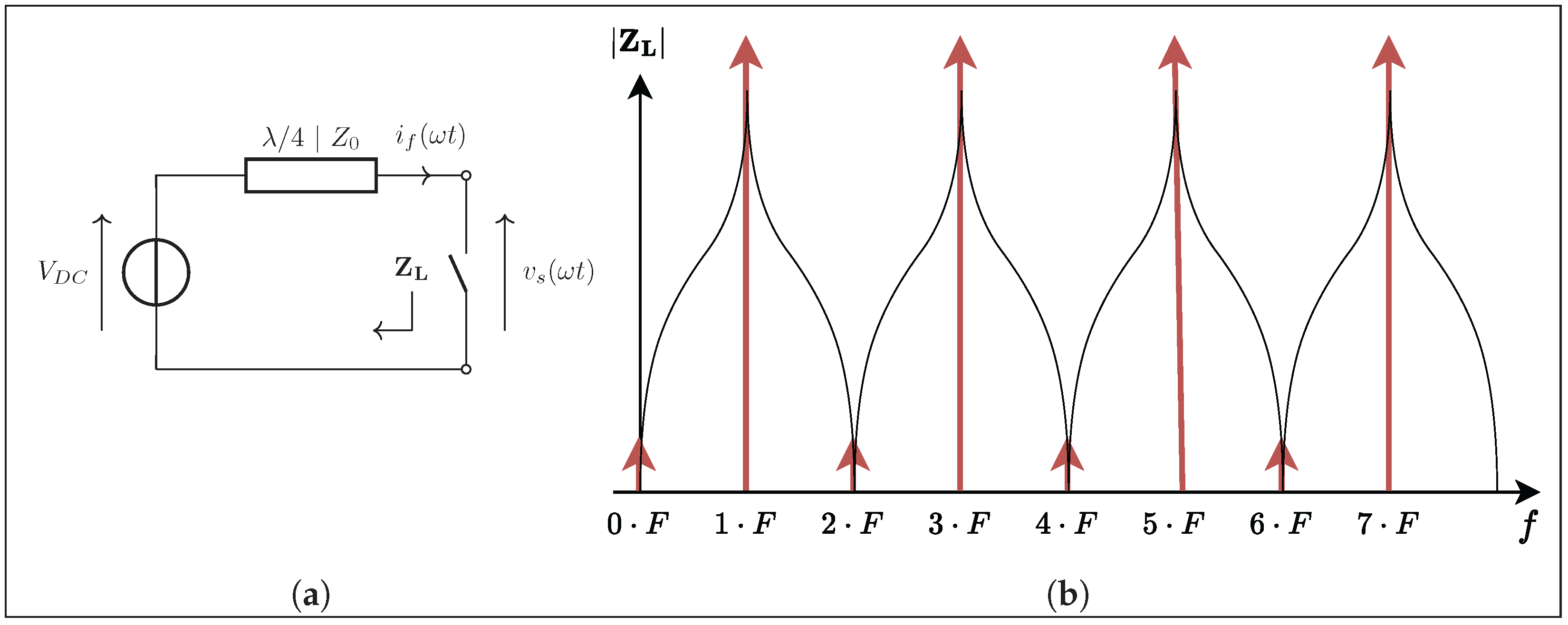
Transmission lines are structures used to convey high-frequency signals, and their input impedance plays a crucial role in determining how they interact with the rest of the circuit. In the case of a lossless transmission line terminated by an ideal voltage source (i.e., with zero internal impedance), the input impedance Z L is given by
Z L = j · Z 0 · tan k · f
where k is a constant that depends on the physical parameters of the line. In our case, and due to the periodic nature of the tangent function, this impedance exhibits resonant behavior: it becomes very large (open circuit) at odd multiples of the fundamental frequency F, and very small (short circuit) at its even harmonics. In such a configuration, the line is referred to as a quarter-wavelength line at frequency F. Figure 3 illustrates this frequency-dependent impedance behavior.
Figure 3. Frequency-dependent impedance behavior of the λ / 4 line. (a) A part of the class EF inverter; (b) theoretical impedance.
Energies 18 05409 g003
In this case, and since the switch operates at a frequency F, the voltage across its terminals v s ( ω t ) is equal to the sum of its odd harmonics:
v s ( ω t ) = V D C + k { 1 , 3 , 5 , 7 , } V s k · sin k · ω t + ϕ v s k
where V s k and ϕ v s k represent the amplitude and phase associated with the k-th harmonic. Hence, the expression of v s ( ω t + π ) can be expressed as follows:
v s ( ω t + π ) = V D C k { 1 , 3 , 5 , 7 , } V s k · sin ( k · ω t + ϕ v s k )
By combining Equations (8) and (9), we obtain
v s ( ω t ) + v s ( ω t + π ) = 2 · V D C
Similarly, the current i f ( ω t ) can only propagate at even harmonics:
i f ( ω t ) = k { 0 , 2 , 4 , 6 , } I f k · sin ( k · ω t + ϕ i f k )
Which directly leads to
i f ( ω t + π ) = i f ( ω t )

2.4. Operating Phases of the Inverter

In following sections, we consider that the switch is closed from 0 to π θ with 0 < θ < π . Table 1 depicts the used driving pattern.
Table 1. Driving pattern of the inverter.
ω t [ 0 , π θ ] [ π θ , π ] [ π , 2 π θ ] [ 2 π θ , 2 π ]
SONOFFOFFOFF
As a consequence, the expression for the duty cycle D, used to drive the switch, can be written as
D = 1 2 θ 2 π
According to this definition, the value of the duty cycle D of the driving signal applied to the switch ranges between 0% and 50%. To provide a clearer understanding of the operating principle of the class EF inverter, we will first analyze each operating phase of the converter in a non-chronological order. Initially, we consider the transistor being ON from 0 to π θ . During this phase, the voltage across the switch v s ( ω t ) can be expressed as:
v s ( ω t ) | 0 < ω t < π θ = 0
As a consequence of Equation (10), the voltage across the switch half a period later can be expressed as
v s ( ω t ) | π < ω t < 2 π θ = 2 · V D C
This preliminary result is essential to understand the following development.
From π to 2 π θ :
During this operating phase, the transistor is OFF so that the current i s ( ω t ) flowing through the switch can be expressed as
i s ( ω t ) = 0
As explained previously by Equation (15), the voltage across the switch v s ( ω t ) is constant and equal to 2 · V D C . As a consequence, the following equation is verified:
d v s ( ω t ) d t = 0
Leading to
i C ( ω t ) = 0
Because of Kirchhoff’s law, the in-line current i f ( ω t ) during this operating phase can be expressed as
i f ( ω t ) = i R ( ω t ) = I · sin ( ω t + ϕ )
From 0 to π θ :
Recall that the switch is ON during this operating phase. Consequently, the voltage v s ( ω t ) is zero, and so is the current i C ( ω t ) flowing through the capacitor:
v s ( ω t ) = 0 i C ( ω t ) = 0
Because of Equation (12), the in-line current must verify
i f ( ω t ) = i f ( ω t + π ) = I · sin ( ω t + ϕ )
Consequently, i s ( ω t ) can be expressed as
i s ( ω t ) = i f ( ω t ) + i R ( ω t ) = 2 · I · sin ( ω t + ϕ )
From π θ to π :
During this operating phase, the switch is OFF so that the i s ( ω t ) current is equal to zero:
i s ( ω t ) = 0
In addition, and in order to respect equations set by (10) and (12) and Kirchhoff’s laws, the in-line current i f ( ω t ) must be equal to zero:
i f ( ω t ) = 0
Since establishing this relation is not straightforward, a detailed proof is provided in the Appendix A. Thus, a differential current i C ( ω t ) circulates through the C s capacitor whose expression is
i C ( ω t ) = i R ( ω t ) = I · sin ( ω t + ϕ )
As a consequence, the v s ( ω t ) voltage must adopt the form described by
v s ( ω t ) = 1 ω C s π θ ω t i C ( ω t ) · d ω t = I ω C s cos ϕ θ + cos ( ω t + ϕ )
From 2 π θ to 2 π :
During this operating phase, the switch is OFF so that the i s ( ω t ) current is equal to zero:
i s ( ω t ) = 0
In addition, and in order to respect equations set by (10) and (12) and Kirchhoff’s laws, the in-line current i f ( ω t ) must be equal to zero:
i f ( ω t ) = 0
Thus, a differential current flows through the capacitor, which can be expressed as
i C ( ω t ) = i R ( ω t ) = I · sin ( ω t + ϕ )
Thus, the voltage across the switch v s ( ω t ) can be obtained by integrating the current i C ( ω t ) , while accounting for the integration constant (= 2 · V D C ):
v s ( ω t ) = 1 ω C s 2 π θ ω t i C ( ω t ) · d ω t + 2 · V D C = 2 · V D C + I ω C s cos ϕ θ cos ( ω t + ϕ )
Table 2 gathers the obtained temporal expressions of voltages and currents for all operating phases.

2.5. Soft-Switching Conditions

The class EF inverter can achieve both zero voltage switching (ZVS) and zero current switching (ZCS) at the switch’s turn-on ( ω t = 2 π ). The ZVS operation of the inverter is defined by the following condition:
v s ( ω t ) | ω t = 2 π = 0
Based on the time-domain evolution of v s ( ω t ) detailed in Table 2, this leads to the following condition, which is necessary to achieve ZVS:
i = I ω C s · V D C = 2 cos ( ϕ ) cos ( ϕ θ )
Similarly, ZCS, which is structurally equivalent to zero derivative voltage switching (ZdVS or ZDS) operation is defined by:
i s ( ω t ) | ω t = 2 π = 0 d v s ( ω t ) d ω t | ω t = 2 π = 0
Again, referring to the temporal waveform of v s ( ω t ) given in Table 2, this condition leads to the following requirement for ZCS operation:
ϕ = 0

2.6. Output Stage

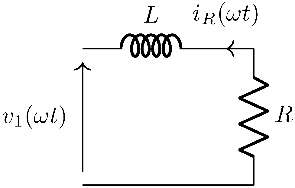
Since the L 1 C 1 filter functions as a bandpass filter tuned to the switching frequency of the inverter, a first-order equivalent circuit of the output stage can be established, where only the fundamental frequency of the v s ( ω t ) voltage is considered. This equivalent circuit is illustrated in Figure 4.
On the one hand, the fundamental voltage of the v s ( ω t ) voltage can be expressed thanks to the first-order equivalent model shown in Figure 4:
v 1 ( ω t ) = R · i R ( ω t ) L · d i R ( ω t ) d t = a 1 · sin ( ω t ) + b 1 · cos ( ω t )
With a 1 and b 1 being equal to
a 1 = L ω · sin ( ϕ ) R · cos ( ϕ ) · I ( 36 ) b 1 = R · sin ( ϕ ) + L ω · cos ( ϕ ) · I   ( 37 )
On the other hand, the a 1 and b 1 coefficients of the fundamental voltage v 1 ( ω t ) of the voltage across the switch v s ( ω t ) can be expressed thanks to Fourier’s theory:
a 1 = 1 π 0 2 π v s ( ω t ) · sin ( ω t ) · d ω t ( 38 ) b 1 = 1 π 0 2 π v s ( ω t ) · cos ( ω t ) · d ω t ( 39 )
Consequently, the obtained expressions for a 1 and b 1 can be equated with those derived from Equations (36) and (37). As a result, two fundamental relations set by Equations (40) and (41) are obtained. These equations connect the various parameters of the class EF inverter for any operating point, provided that assumptions (H1) to (H6) hold true.
r · i · cos ( ϕ ) x · i · sin ( ϕ ) = 4 π i π · [ 4 · sin 4 θ 2 · cos ( ϕ ) + sin ( ϕ ) · θ + sin ( θ ) · ( cos ( θ ) 2 ) ]   ( 40 ) r · sin ( ϕ ) + x · cos ( ϕ ) = 1 π · θ · cos ( ϕ ) sin ( θ ) · cos ( θ ϕ ) ( 41 )
At this stage of the study, four key equations have been established to describe the operation of the class EF inverter:
  • Two design equations, given by (40) and (41), which characterize the inverter’s behavior for a given load.
  • Two equations defining the necessary conditions for soft-switching operation (ZVS and ZCS), provided in (32) and (34).
The next objective of the study is to constrain the inverter design equations using the soft-switching conditions, thereby deriving the design equations specific to the class EF inverter operation under ZVS and/or ZCS. To this end, the approach consists primarily in substituting Equations (32) and/or (34) into Equations (40) and (41), followed by analytical simplification wherever possible.

3. Optimal and Non-Optimal Behavior of the Class EF Inverter

3.1. Optimally Loaded Class EF Inverter
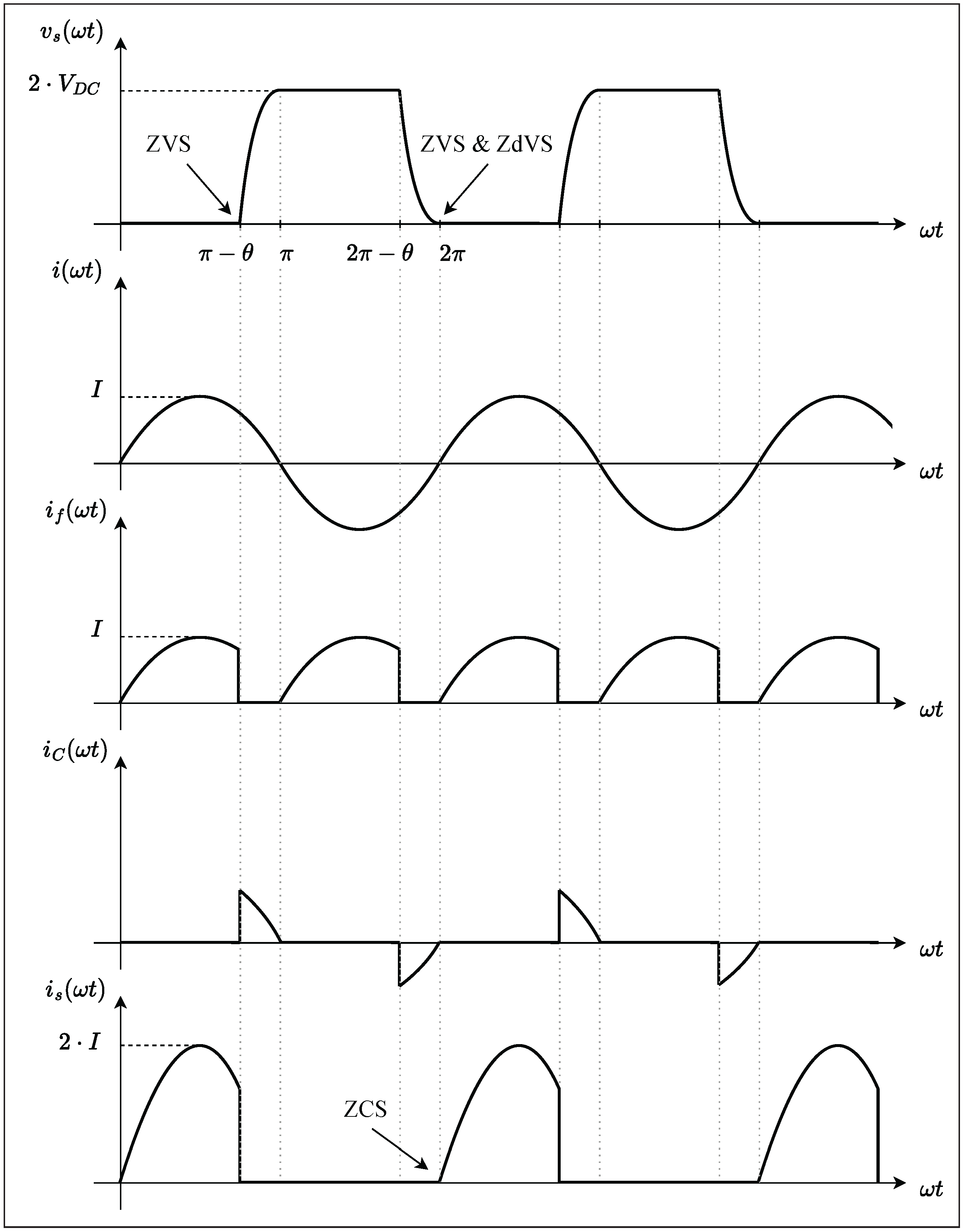
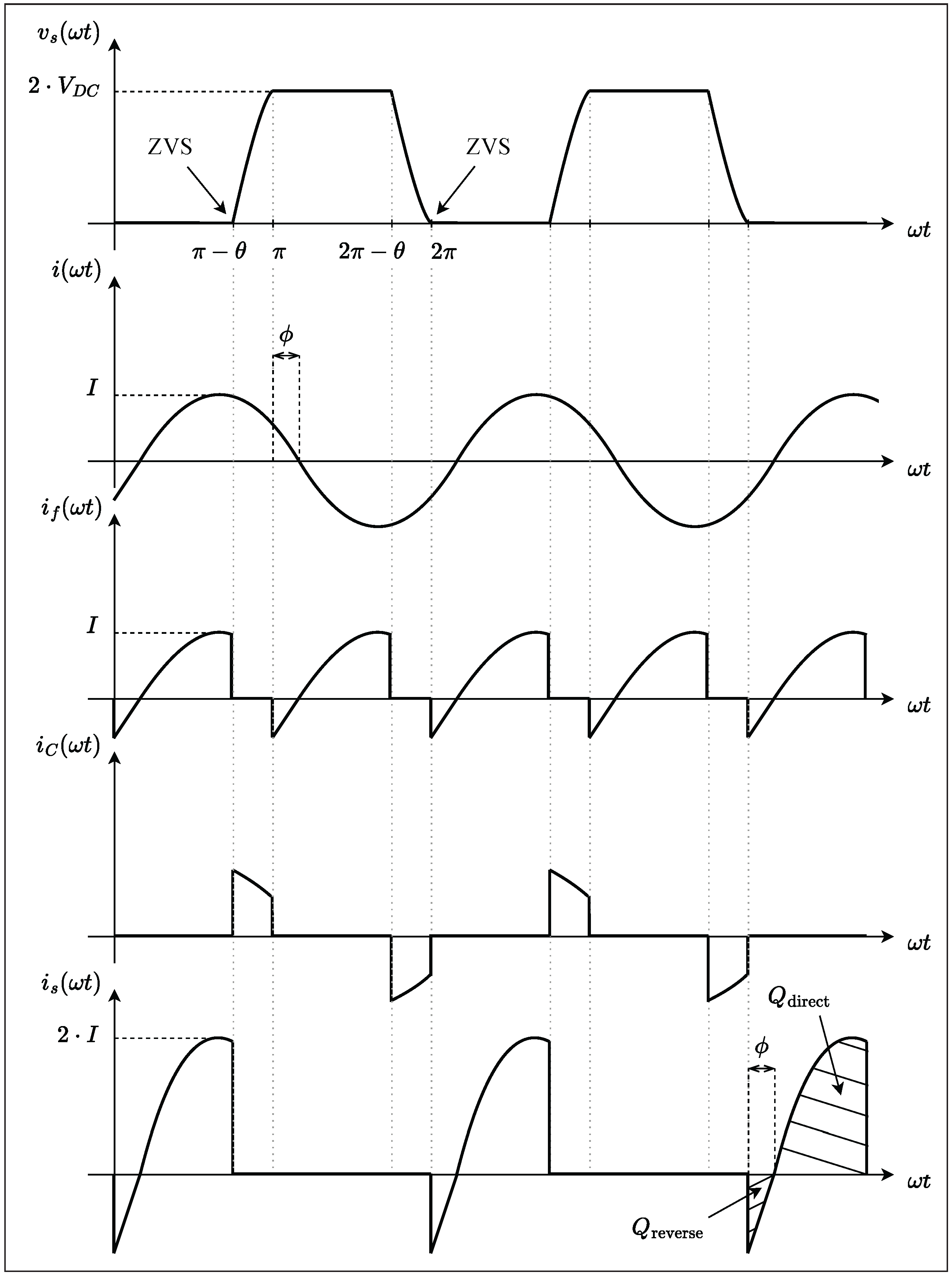
We begin by examining the specific case of a class EF inverter operating simultaneously under ZVS and ZCS, with the theoretical waveforms shown in Figure 5. Since both soft-switching conditions are simultaneously achieved in this scenario, it is referred to as the optimal case.
Figure 5. Theoretical waveforms at the optimal operating point.
Energies 18 05409 g005
In this case, since both ZVS and ZCS conditions are simultaneously satisfied, Equations (32) and (34) can be combined to express i as follows:
i = 2 1 cos ( θ )
Consequently, combining Equations (34) and (40)–(42) allows us to write both following equations, where θ can be related to the duty cycle D using Equation (13):
r = 1 π · sin 2 ( θ )   ( 43 ) x = 1 π · θ sin ( θ ) · cos ( θ ) ( 44 )
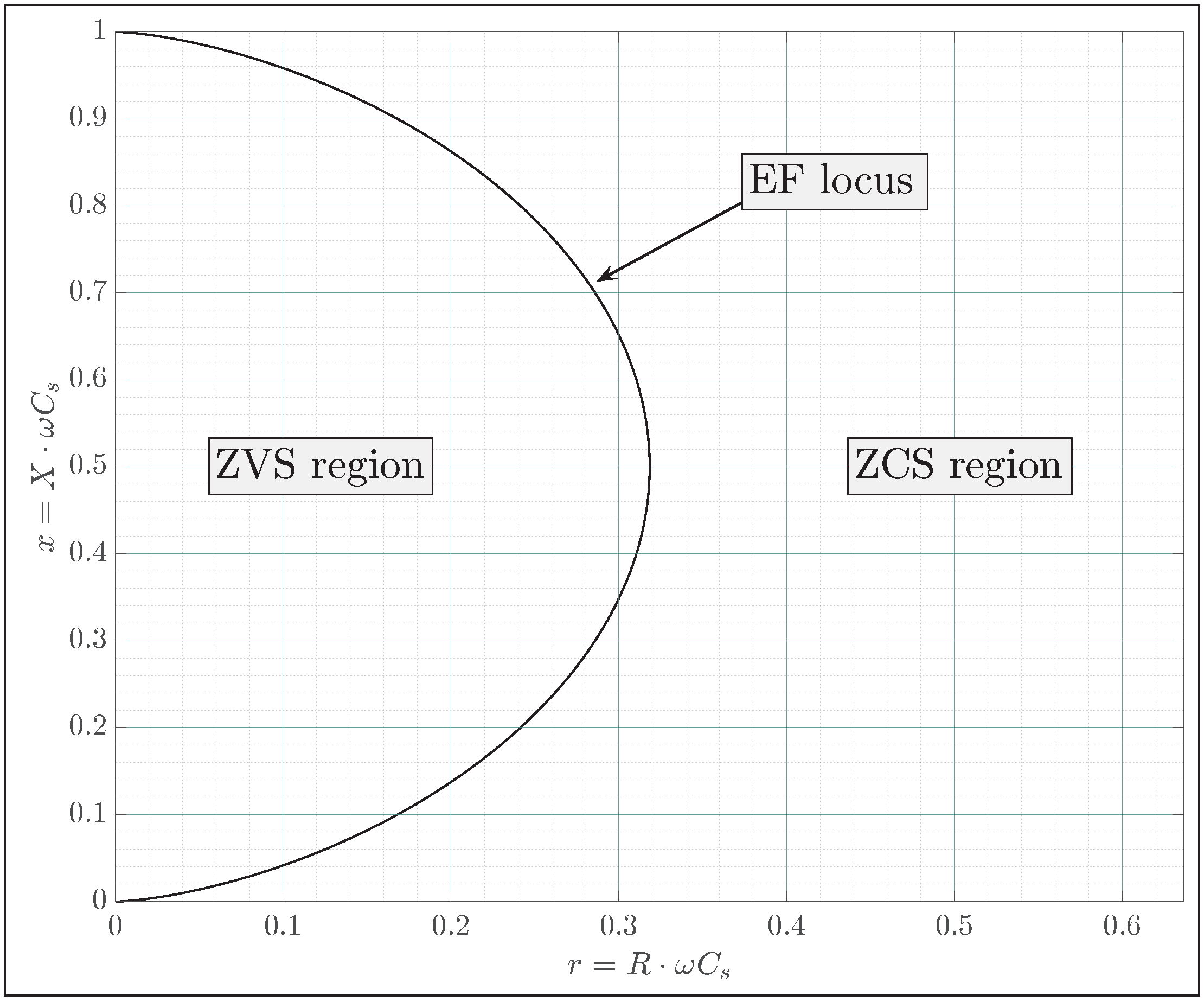
This means that the class EF inverter will operate in both ZVS and ZCS if the conditions specified by Equations (43) and (44) are both satisfied. Since these two equations are parametrized with the value of θ , it is possible to plot them in a single ( r , x ) plan. The resulting curve, which has been named the EF locus, is plotted on Figure 6.
Figure 6. Required value of x as a function of r to allow optimal ZVS and ZCS soft-switching operations.
Energies 18 05409 g006
In addition, the value of p in an ideally tuned class EF inverter can be determined using the expression for i, which is given by Equation (42):
p = 1 2 · r · i 2 = 2 π · 1 tan 2 θ 2
Optimal load conditions correspond to the design point where the switch operates under ideal ZVS/ZdVS conditions (EF locus). In practical applications, it may be necessary to design a class EF inverter whose operating point does not lie exactly on the EF locus defined in Figure 6. Such scenarios are referred to as non-optimal operating points, which can be categorized into two distinct regions:
  • ZCS region: occurs when the R · ω C s product exceeds the optimal value.
  • ZVS region: occurs when the R · ω C s product is below the optimal value.
The primary goal of the following subsections is to derive analytical expressions that characterize the behavior of the class EF inverter in these two regions as a function of the operating point’s location in the ( r , x ) plane, i.e., based on the load impedance. As previously outlined, this will be achieved by substituting one of the two soft-switching conditions—Equations (32) or (34), depending on the considered region of the plane—into the inverter design Equations (40) and (41).

3.2. ZCS Region

In the ZCS region, where the product R · ω C s exceeds the optimal value, there is a reduction in the circulating currents within the inverter. This results in an inability to maintain ZVS at the turn-on of the switch. However, ZCS can still be maintained in this region, as the derivative of v s ( ω t ) does reach zero. Figure 7 shows the theoretical waveforms of a class EF inverter operating in the ZCS region. Note the presence of a discontinuity in the voltage v s ( ω t ) in this figure. This discontinuity arises from the analysis of piecewise continuous functions that are not defined at ω t = π θ , ω t = π , ω t = 2 π θ , and ω t = 2 π .
In this work, we denote the voltage across the switch just before it turns on as V 0 (see Figure 7):
V 0 = v s ( ω t ) | ω t = 2 π
Note that, in the specific case of an inductive load impedance ( X = L · ω > 0 ) , V 0 is lower than the maximum voltage across the switch. Since ZCS is maintained, Equation (34) remains true. However, Equation (32) is no longer valid because it reflects the ZVS condition of the class EF inverter, which is not achieved in this scenario. As a result, Equations (40) and (41) are revised to
r = 4 π · 1 i sin 4 θ 2 ( 47 ) x = 1 π · θ sin ( θ ) · cos ( θ ) ( 48 )
Then, the expression of i can be found using Equation (47):
i = 4 π · r + 4 · sin 4 θ 2
Using the new expression of i for a class EF inverter operating under ZCS conditions only, the normalized output power p delivered by the inverter can be expressed as
p = 1 2 · r · i 2 = 8 · r π · r + 4 · sin 4 θ 2 2
Regarding the value V 0 as defined by Equation (46), it can be expressed using the following relationship derived from Equation (30):
V 0 = 2 · V D C + I ω C s · cos ( θ ) 1
Using the expression of i obtained in Equation (49) leads to
v = V 0 2 · V D C = 1 + 2 · cos ( θ ) 1 π · r + 4 · sin 4 θ 2
Thus, this v index, which again depends only on the values of r and x, quantifies the deviation between the optimal switching condition—where both ZVS and ZCS are achieved—and the suboptimal condition realized by the class EF inverter operating under ZCS only. Since the variables p, D, and v in the ZCS region, which are provided by Equations (13), (50) and (52), respectively, are functions of r and θ only, and since θ depends solely on x in the ZCS region according to Equation (48), it follows that p, D, and v depend exclusively on r and x in the ZCS region.

3.3. ZVS Region

In the ZVS region, where the R · ω C s product is lower than its optimal value, the circulating currents within the inverter increase. This rise in current leads to a scenario where ZCS would theoretically occur when v s ( ω t ) should be negative. However, this situation is not possible due to reverse conduction in the actual switch. As a result, only ZVS can be maintained in this region. Theoretical waveforms for a class EF inverter operating in the ZVS region are depicted in Figure 8. Because ZCS is no longer achievable, the value of ϕ cannot be set to zero using Equation (34), as it was previously. However, the ZVS condition, given by (32), is still valid. Consequently, the design equations of the inverter, which were previously expressed by Equations (40) and (41), can now be adjusted to account for the ZVS condition only:
r = 1 π · sin ( θ ) · sin ( θ 2 · ϕ ) ( 53 ) x = 1 π · θ sin ( θ ) · cos ( θ 2 · ϕ ) ( 54 )
Therefore, the normalized output power p can be expressed as a function of ϕ and θ based on the expressions for r and i, given by Equations (53) and (32), respectively:
p = 1 2 · r · i 2 = 2 π · sin ( θ ) · sin ( θ 2 · ϕ ) ( cos ( ϕ ) cos ( ϕ θ ) ) 2
Figure 8. Theoretical waveforms in the ZVS region.
Energies 18 05409 g008
In addition, the amount of electrical charge conducted in the reverse direction through the switch—see Figure 8—can be expressed as
Q reverse = 1 ω 0 ϕ i s ( ω t ) · d ω t = 2 · I ω cos ( ϕ ) 1
Additionally, the amount of electrical charge conducted directly through the switch can be expressed as follows:
Q direct = 1 ω ϕ π θ i s ( ω t ) · d ω t = 2 · I ω 1 + cos ( ϕ θ )
Finally, we define a q factor as the ratio of the electrical charge conducted in the reverse direction to the charge conducted directly through the switch. By analyzing the value of this q factor, one can rapidly identify the difference between the optimal switching condition, where only direct electrical charges flow through the switch, and the ZVS switching condition:
q = | Q reverse | Q direct = 1 cos ( ϕ ) 1 + cos ( ϕ θ )
Consequently, since the variables p, D, and q in the ZVS region, as provided by Equations (13), (55) and (58), respectively, are functions of θ and ϕ only—two variables which themselves are functions of r and x in the ZVS region according to the system of equations formed by (53) and (54)—it follows that p, D, and q depend exclusively on r and x in the ZVS region.
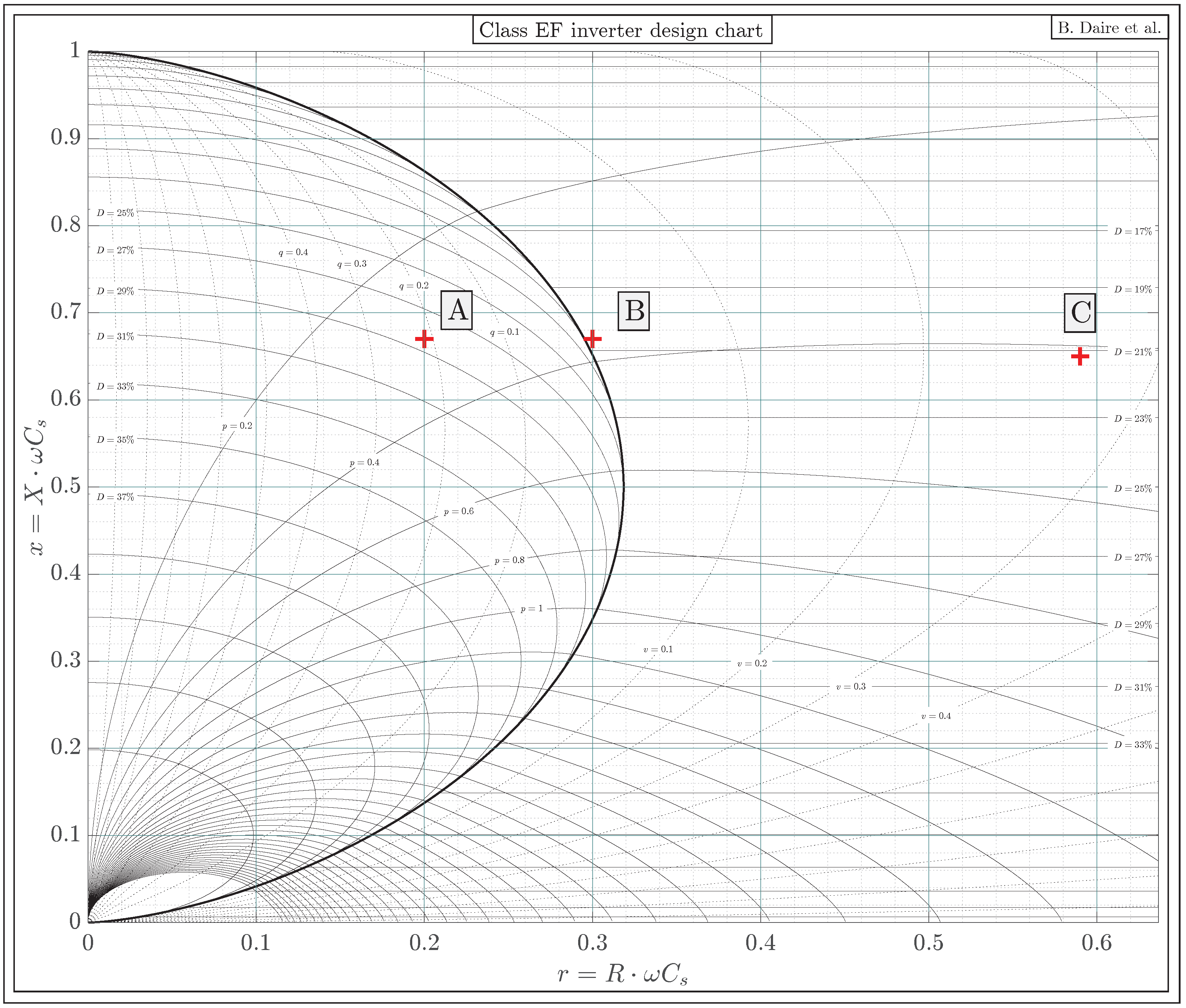
Since all calculated parameters for each region of the ( r , x ) plan shown on Figure 6 are nonlinear functions of r and x only, they can be consolidated into a single plot to create a design chart for analyzing the behavior of the class EF inverter whether it is loaded with its optimal impedance or not. This chart links the values of D, p, v and q in the class EF inverter for any value of r and x, facilitating rapid design and load variation analysis (Additional resources, including an interactive version of the chart and download links, are available online at bdaire.github.io (https://bdaire.github.io/research_chart_svg-interactif.html), accessed on 16 September 2025).

4. Experimental Validation

This section aims to demonstrate the applicability of the proposed analytical development to real-world converter through the implementation of a 15 MHz—25 VDC input voltage class EF inverter. Three different operating points are tested, each one being located in a different region of the chart:
  • Operating point ‘A’: located in the ZVS region
  • Operating point ‘B’: located on the EF locus
  • Operating point ‘C’: located in the ZCS region

4.1. Implementation of the Class EF Inverter

Sizing of class EF inverter comprises two steps namely the sizing of the input network which is composed of the quarter-wavelength transmission line and the sizing of the output network which is composed of L 1 , C 1 , L and R. Figure 9 shows the two networks, as well as impedances associated with each of them.
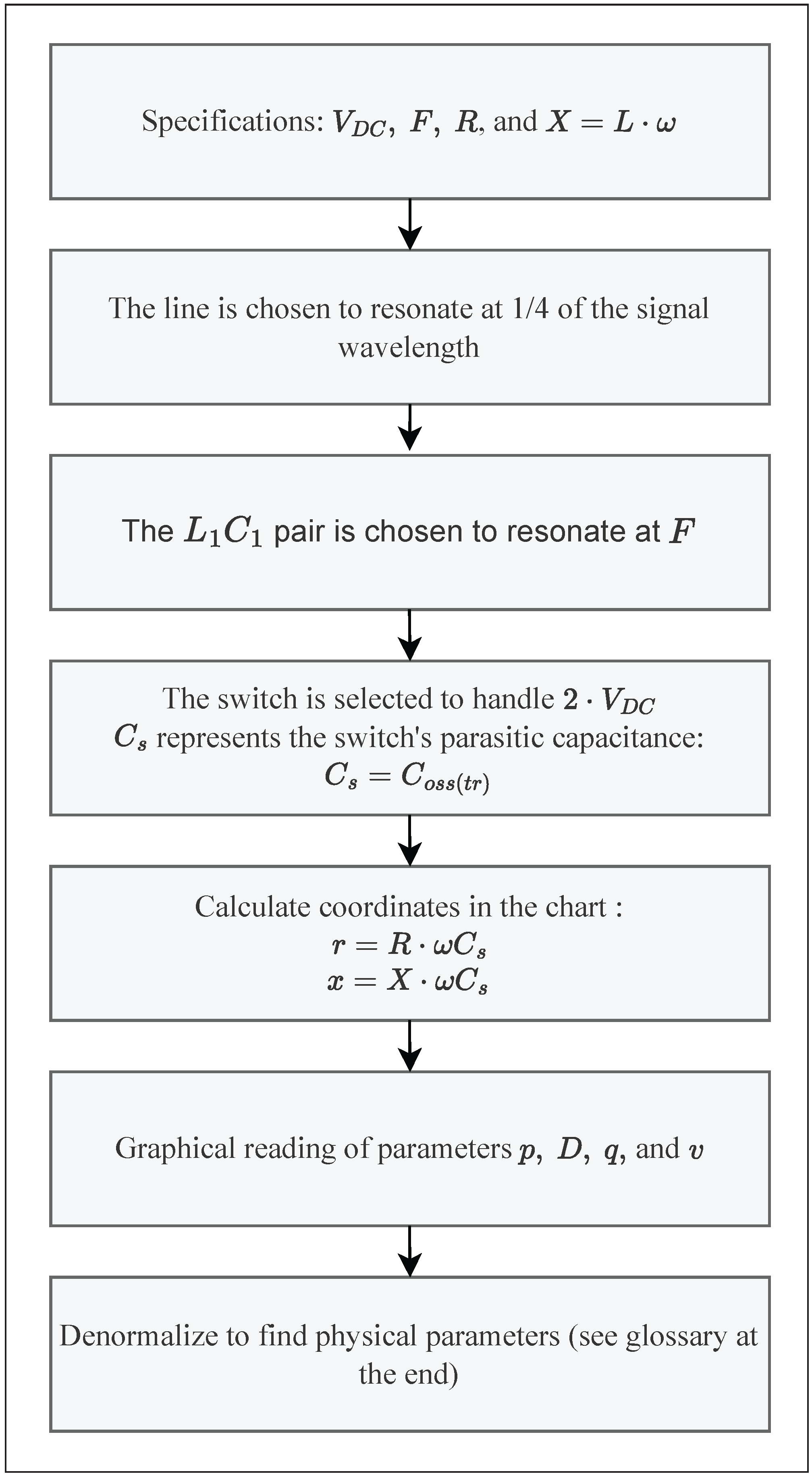
The flowchart shown in Figure 10 provides a concise overview of the key steps in the design of the class-EF inverter that we will follow.
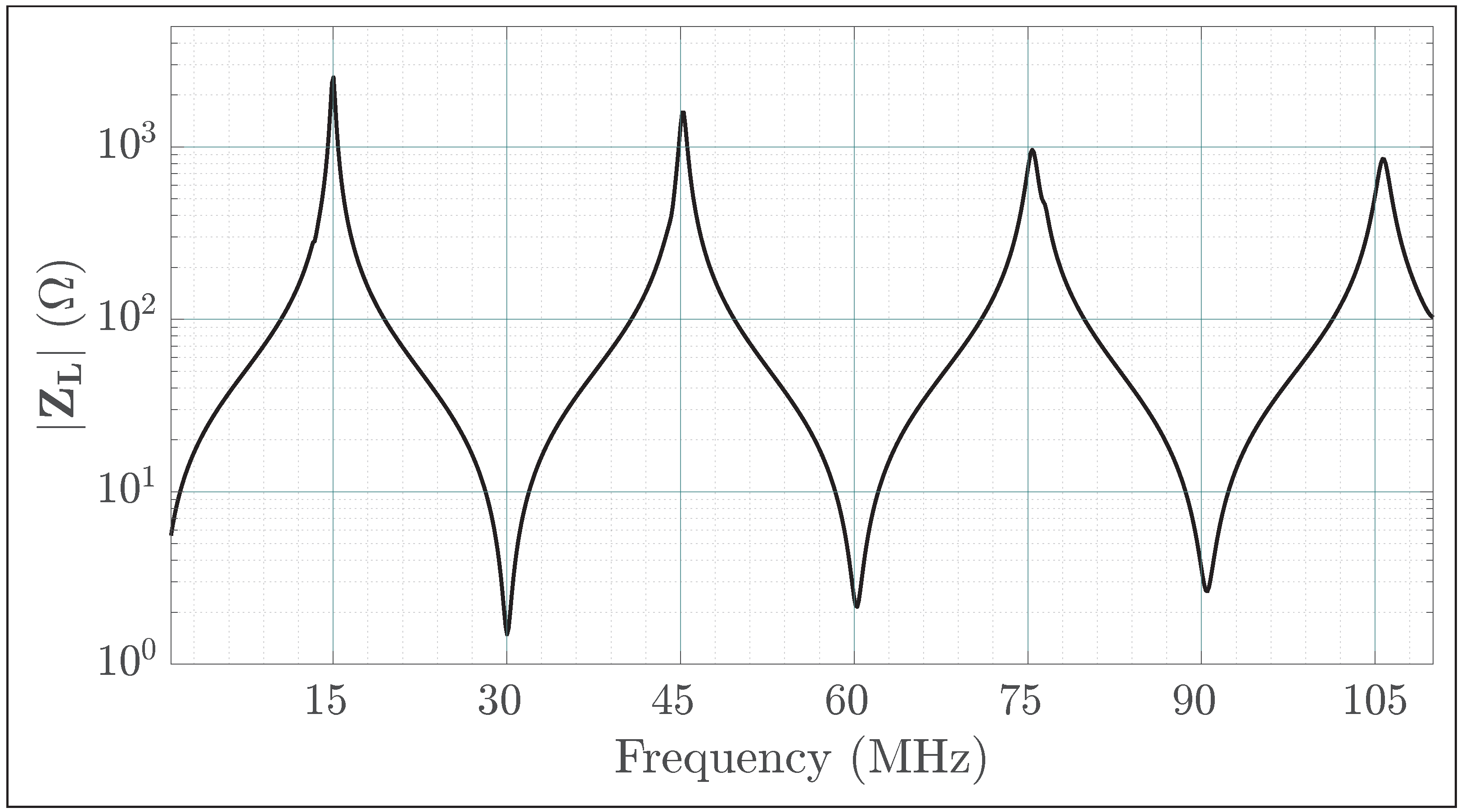
The choice has been made to use a 3.5 m RG303/U PTFE coaxial cable from QAXIAL short-circuited at input DC voltage side with two CKG57NX7R2E105M500JH from TDK and two CB037E0104KBA capacitors from KYOCERA AVX in order to implement the quarter-wavelength transmission line. The measured magnitude of Z L is plotted in Figure 11. All impedances were measured using a 4294A impedance meter from Agilent. Admittedly, the use of a 3.5 m coaxial cable to implement a quarter-wavelength line at 15 MHz is impractical and bulky for real applications. However, this unconventional choice was motivated for three reasons:
  • The need to validate the analytical derivation under quarter-wavelength conditions, while staying within the bandwidth of our oscilloscope.
  • The opportunity to present, to the best of our knowledge, unprecedented experimental waveforms of this type
  • Providing a direct justification for the substitution with discrete reactive components: the line is often replaced by an equivalent network made of lumped-elements, as detailed in Section 4.4.
This original observation constitutes a key contribution of the present work.
Since the maximum voltage across the switch is expected to reach 2 · V D C = 50 V, the choice has been made to use a 100 V, 90 A transistor (GS61008P from Infineon). The C s capacitor is only composed of the time-related parasitic capacitance of the switch [33]. According to the datasheet of the device, the value of this capacitance from 0 to 50 V is equal to 385 pF. In addition, the choice has been made to reach three different operating points namely ‘A’, ‘B’ and ‘C’, each one being located in a different region of the chart. To achieve this, the load resistor was modified (while remaining within the Caddock MP9100 series), whereas all other components were kept unchanged. Table 3 lists the components used in order to implement each operating points.
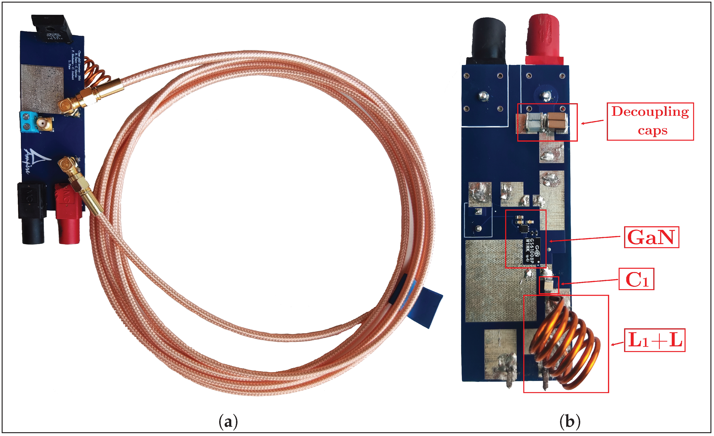
Figure 12 shows the measured impedance Z out for the three operating points. Note that the load offers a high absolute value of | Z out | impedance to high-order harmonics as desired (see assumption (H6)). Figure 13 shows the realized class EF inverter.

4.2. Extraction of Key Parameters Using the Design Chart

Using Figure 12, it is possible to read the corresponding values of | Z out | and arg ( Z out ) for each operating point and to calculate the corresponding values of R and X at the switching frequency (15 MHz). Table 4 shows the results of this identification, as well as the corresponding values of r = R · ω C s and x = X · ω C s .
Then, each operating point can be placed on the design chart knowing their respective coordinates (i.e., values of r and x). The results of this process are shown in Figure 14.
As a consequence, several parameters can be read directly on the chart:
  • The value of the duty cycle D, using the D-curves, that must be used in order to maintain soft switching;
  • The value of p, using p-curves, from which can be deduced the corresponding power delivered to the load using Equation (5);
  • The value of v or q, using the v-curves or q-curves whether the operating point is located in the ZVS region or in the ZCS region. These values can be used in order to calculate the value of the V 0 voltage at which the switch is turned on or the amount of electrical charges that are reverse-conducted through the switch using Equations (52) or (58).
Table 5 shows the resulting parameters for each operating point.

4.3. Experimental Results

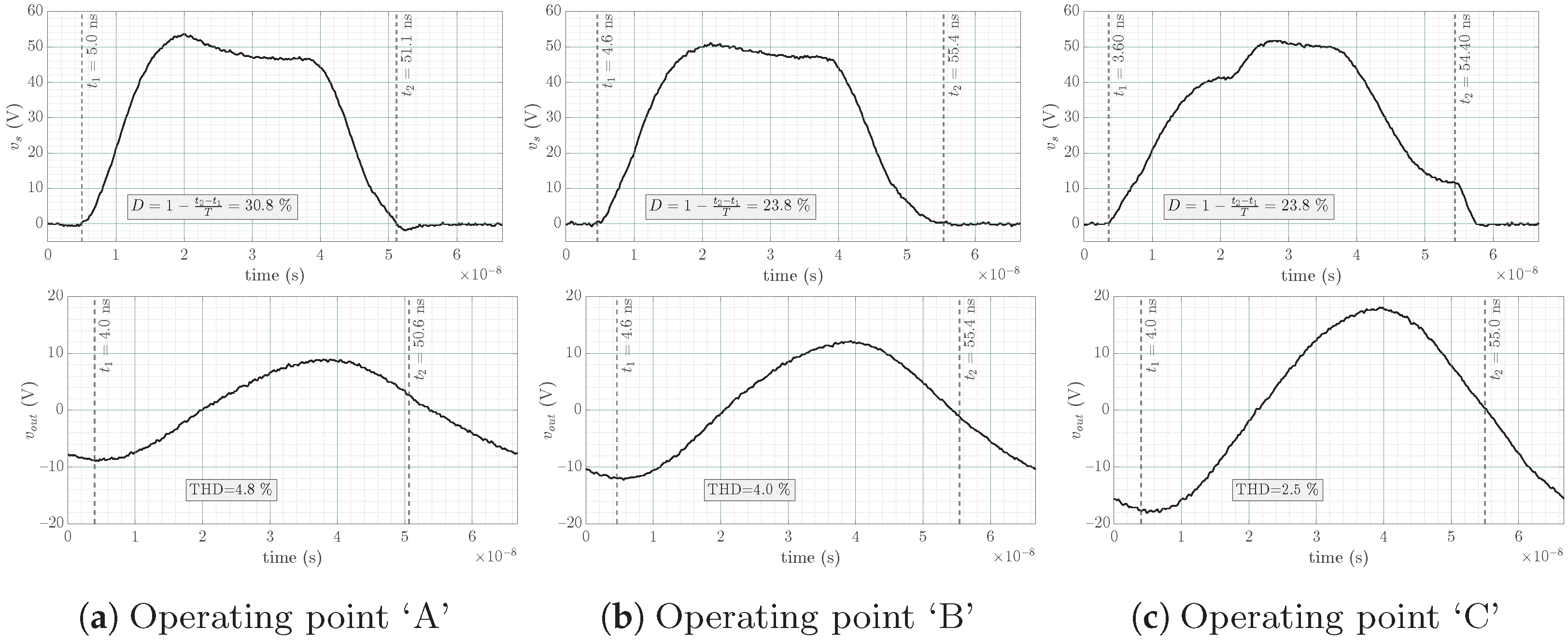
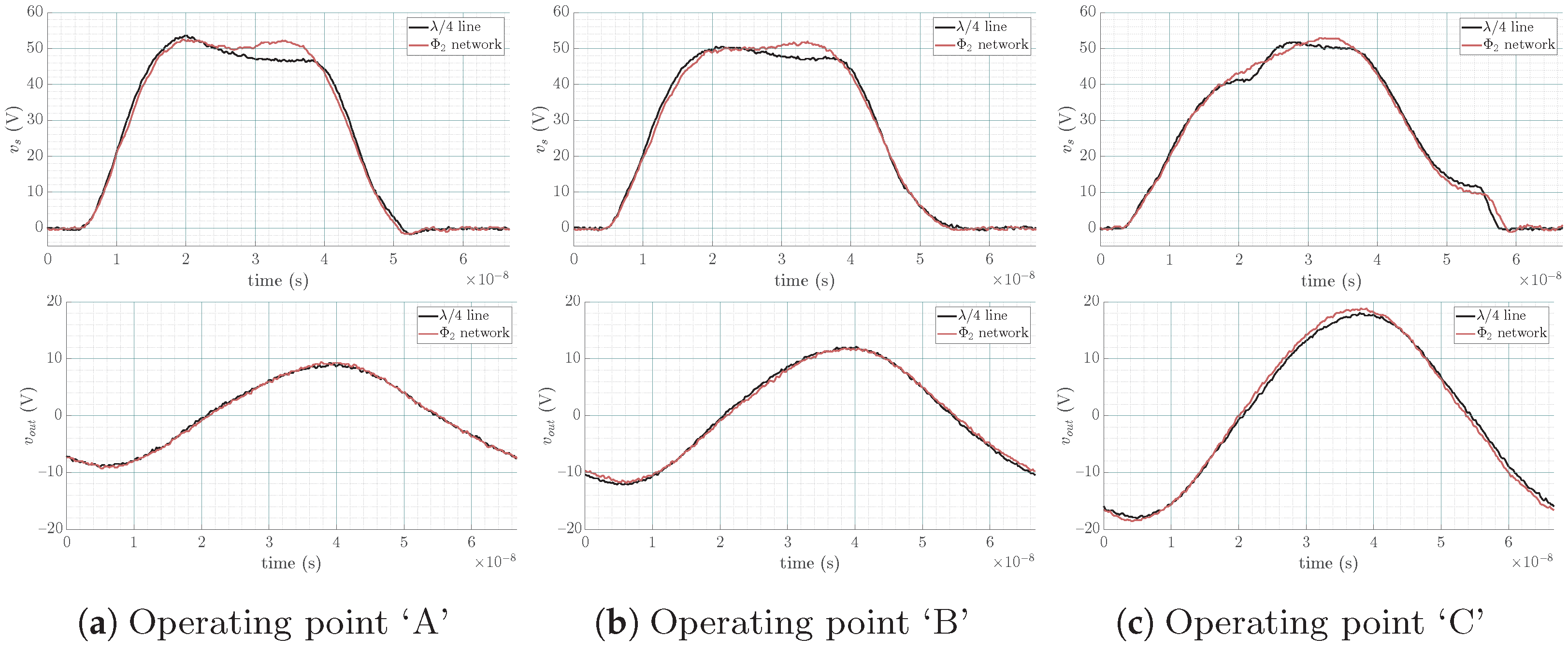
All waveforms were recorded by using a 1 GHz—3.9 pF passive probe (TPP1000 by Tektronix) in conjunction with a 1 GHz Tektronix MSO 5104 Mixed Signal Oscilloscope. Figure 15 illustrates the experimentally measured switch voltage v s ( ω t ) and output voltage v o u t ( ω t ) (with Total Harmonic Distortion, THD, annotated) corresponding to the three operating points. The following key observations were made:
  • Only ZVS is performed at operating point ‘A’ as predicted using the chart since this operating point is located in the ZVS region.
  • Only ZCS, which is structurally equivalent to zero derivative voltage switching (ZdVS or ZDS) operation, is performed at operating point ‘C’ as predicted using the chart since this operating point is located in the ZCS region.
  • Both ZVS and ZCS (⇔ZdVS) are performed at operating point ‘B’ as predicted using the chart, since this operating point is located on the EF locus.
Table 6 presents a comparison between the predicted duty cycle required to maintain soft switching, as derived from the design chart, and the actual duty cycle extracted from the measured switch voltage. In addition, this table gathers the actual output power delivered by the converter that was measured following the procedure outlined in [34], and the predicted one, as derived from the chart.
In addition, the V 0 voltage at operating point ‘C’ was measured to be 12 V, which is 7.7% lower than the predicted value of 13 V based on the design chart. It should be noted that measuring the current through the switch, i s ( ω t ) , was not feasible due to the high fundamental frequency, which exceeds the capabilities of available measurement systems. Moreover, current sensor could add some parasitics that deteriorate the operation of the converter. Consequently, the q factor for operating point ‘A’ cannot be directly determined through measurement.

4.4. Lumped Analogs

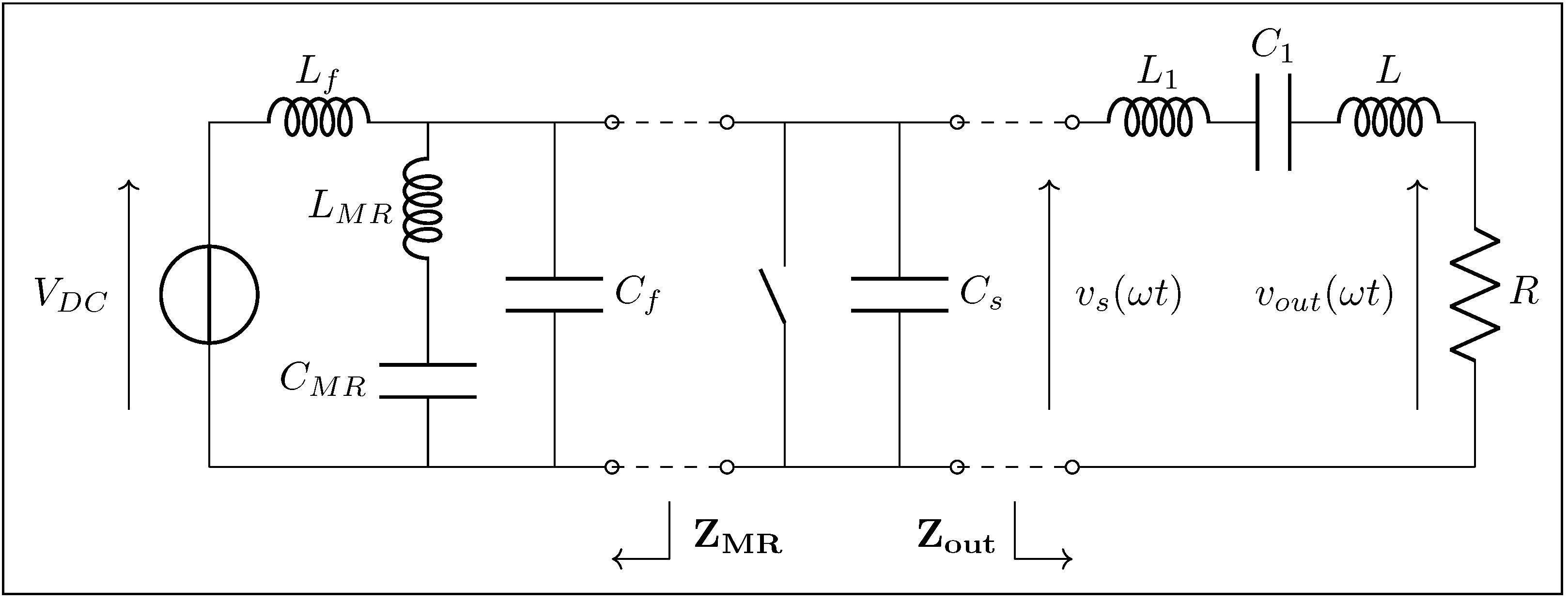
Due to the impracticality of using bulky quarter-wavelength transmission lines in real-world power conversion applications, it is common to replace them with a lumped-element equivalent network that approximates the line’s impedance for a limited number of harmonics [35,36]. Figure 16 presents a specific implementation of the quarter-wavelength transmission line using lumped-elements only.
Figure 16. A lumped transmission line analog.
Energies 18 05409 g016
This network can effectively replicate the behavior of the transmission line if the following requirements are satisfied [36]:
C M R = 15 16 · C f ( 59 ) L M R = 1 15 · π 2 · F 2 · C f ( 60 ) L f = 1 9 · π 2 · F 2 · C f ( 61 )
Note that the corresponding class EF inverter implemented with this type of input network is most commonly known as class Φ 2 inverter in the literature [7]:
Figure 3 shows the proposed switched-mode resonant inverter, which we term the Φ 2 inverter. It is closely related to the class Φ [EF in this work] inverter of [5], [25] [respectively [4,35] in this work], but has the high-order transmission-line network replaced by the low-order resonant network illustrated in Figure 4 [Figure 16 in this work] (or an equivalent network).”
J. Rivas in [7]
Figure 17 depicts the overall circuit of the class Φ 2 inverter, with its key impedances annotated.
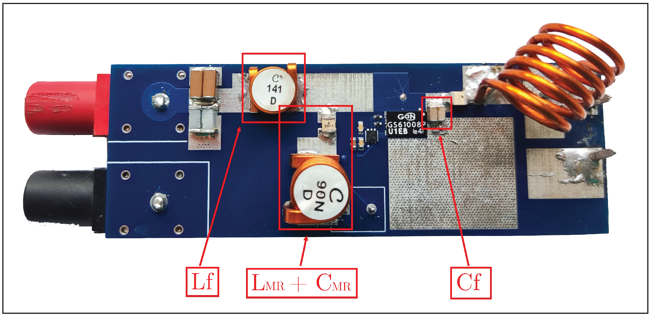
In this section, we aim to briefly demonstrate the applicability of the proposed analysis to the class Φ 2 inverter by replacing the quarter-wavelength transmission line with a Φ 2 -type input network, as illustrated in Figure 18. Note that the used printed circuit board was designed to handle both inverters so that apart from the input network, the other components of the PCB remain unchanged compared to the previous section, as shown in Figure 13b and Figure 18. The used components C M R , L M R , C f , and L f are detailed in the accompanying Table 7.
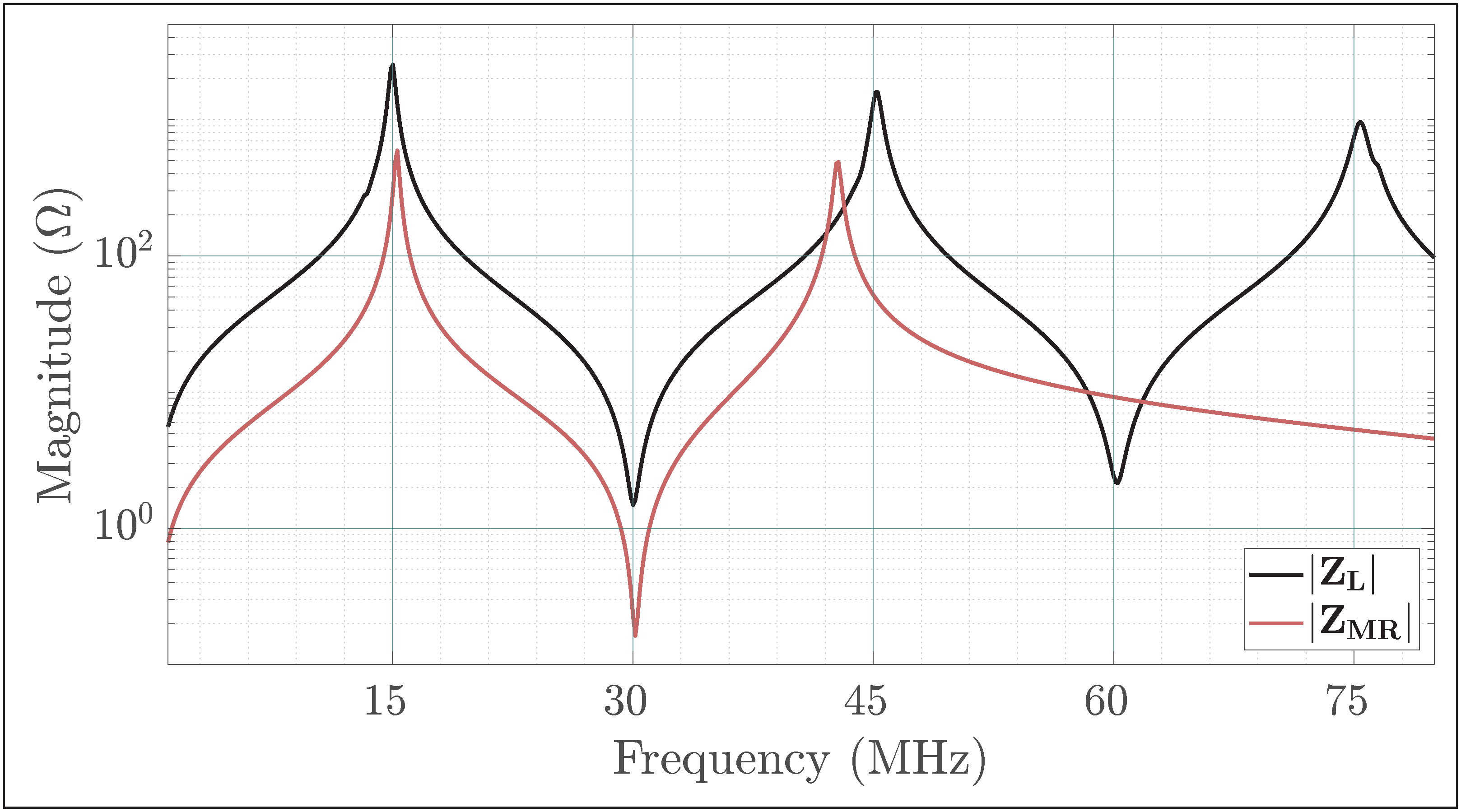
The measured impedance Z MR is depicted in Figure 19, where it is superimposed with the previously characterized transmission line impedance Z L for comparison purposes. A slight misalignment occurs between the two networks at the third impedance peak (45 MHz). This phenomenon is attributed to the challenging implementation of the Φ 2 -type input network. Nevertheless, the absolute value of the impedance of the lumped-element network remains sufficiently high at 45 MHz to ensure an open-circuit for the third harmonic.
Finally, Figure 20 shows the measured voltages v s ( ω t ) and v o u t ( ω t ) for the three operating points under consideration. The waveforms obtained using a class Φ 2 lumped analog network are consistent with those produced by a transmission line, aside from several high-frequency harmonics, as the lumped network accurately reproduces the line’s behavior for the first three harmonics only.

5. Discussion

5.1. Limitations

5.1.1. Sensitivity to Parasitic Elements and Component Tolerances

A key limitation of the proposed analytical models arises from the following idealized assumptions:
  • Negligible parasitic elements (e.g., stray inductance, ON-state resistance).
  • Fixed transistor capacitance C s , representing the full switching range from 0 to 2 · V D C .
  • Infinite quality factor for the L 1 C 1 output filter.
While standard in resonant converter analysis, these assumptions can affect real-world performance. Parasitic inductances near the switch may introduce waveform distortions or even cause device failure [37]. Component tolerances can also lead to deviations from predicted performance. Achieving results consistent with the design chart requires careful impedance characterization and experimental validation, as demonstrated in Section 4. These considerations apply to any methodology based on analytical modeling.

5.1.2. Generality of the Design Chart

Although several operating points were tested experimentally, the range of conditions explored is limited:
  • Restricted coverage of the design chart: extreme regions of the chart were not experimentally validated. However, the tested conditions reflect realistic operating scenarios.
  • Fixed design parameters: experiments were conducted at a single input voltage ( V D C = 25 V), transistor capacitance ( C s = 385 pF ), and switching frequency (15 MHz). Accuracy outside this parameter set is not guaranteed.
Nevertheless, we also implemented a 30 MHz, 80 W converter, demonstrating that the design chart remains predictive even at higher frequency and power levels, with limited sensitivity to parasitic elements. Complementary ideal-circuit simulations under varied conditions consistently align with the chart, suggesting scalability within the theoretical assumptions.

5.2. Expected Benefits and Perspectives

5.2.1. Comparison with Existing Design Methodologies

The design chart provides a fast, visual alternative to conventional approaches such as iterative simulations, numerical time-domain analysis, or machine-learning-based prediction, while based on ideal assumptions, the chart’s predictions closely match experimental measurements, validating the proposed analytical framework.
A practical strategy involves using the chart for an initial design estimate, followed by refinement using numerical methods or simulations that account for parasitic effects. This hybrid approach combines the simplicity and speed of the chart with the accuracy required for practical applications.

5.2.2. Design of Novel Conversion Architectures

The user-friendly format of the design chart enables the straightforward visualization of operating conditions, supporting the development of load-independent class EF inverter-based converters and their lumped-element analogs. By plotting the operating point as the load varies, designers can:
  • Align with a D -curve in the ZVS or ZCS region, enabling soft switching over a wide load range without modifying the duty cycle.
  • Align with the EF locus to maintain simultaneous ZVS and ZCS, with duty cycle adjustment per load as needed.
The chart also aids resonant DC/DC converter design by mapping rectifier input impedance at the switching frequency. These capabilities highlight promising directions for future research and applications in high-frequency power electronics.

6. Conclusions

This paper presents a systematic analytical methodology for class EF inverters and their lumped-element derivatives, consolidated in a single, user-friendly design chart. The proposed approach enables rapid and intuitive sizing of inverters under a wide range of load conditions.
Experimental validation was conducted on both a 15 MHz inverter with a quarter-wavelength transmission line and a Φ 2 inverter using discrete reactive elements. Measured parameters closely match predictions from the design chart, confirming its accuracy and generality.
The design chart provides several practical benefits: reduced design iteration time, fast evaluation of operating points under soft-switching constraints, and support for the development of novel high-frequency power conversion architectures.
Looking forward, this methodology can accelerate the design of high-power, high-frequency converters in both research and industry, while serving as an effective tool for understanding complex resonant behaviors and soft-switching phenomena.

Author Contributions

Conceptualization, B.D., C.M., F.S., C.J. and L.P.; Methodology, B.D., C.M., F.S., C.J. and L.P.; Validation, B.D., C.M., F.S., C.J. and L.P.; Formal analysis, B.D., C.M., F.S., C.J. and L.P.; Writing—original draft, B.D., C.M., F.S., C.J. and L.P.; Writing—review & editing, B.D., C.M., F.S., C.J. and L.P. All authors have read and agreed to the published version of the manuscript.

Funding

This research received no external funding.

Data Availability Statement

The original contributions presented in this study are included in the article. Further inquiries can be directed to the corresponding author.

Conflicts of Interest

The authors declare no conflicts of interest.

Appendix A

Table A1. Glossary of used variables.
NameDefinitionExpression
rNormalized resistance r = R · ω C s
xNormalized reactance x = X · ω C s
iNormalized output current i = I ω C s · V D C
pNormalized output power p = P ω C s · V D C 2
vNormalized V 0 voltage v = V 0 2 · V D C
qNormalized reverse charge q = | Q reverse | Q direct
Analytical derivation of Equations (24) and (28)
Let us first recall that the operation of the class EF inverter is governed by the following three equations:
v s ( ω t ) + v s ( ω t + π ) = 2 · V D C ( A 1 ) i f ( ω t ) = i f ( ω t + π ) ( A 2 ) i f ( ω t ) + i ( ω t ) = i s ( ω t ) + i C ( ω t ) ( KCL )     ( A 3 )
We begin by differentiating Equation (A1) with respect to t:
d v s ( ω t ) d t + d v s ( ω t + π ) d t = 0
which naturally leads to the following result:
C s · d v s ( ω t ) d t + C s · d v s ( ω t + π ) d t = 0
Alternatively:
i C ( ω t ) + i C ( ω t + π ) = 0
Let us now turn our attention to Equation (A3) and apply a phase shift of π :
i f ( ω t + π ) + i ( ω t + π ) = i s ( ω t + π ) + i C ( ω t + π )
Now, by reusing the results from Equations (A2) and (A6), and noting that the current i ( ω t ) is sinusoidal—hence i ( ω t + π ) = i ( ω t ) —it is straightforward to show that
i f ( ω t ) i ( ω t ) = i s ( ω t + π ) i C ( ω t )
By summing Equations (A3) and (A8), we obtain
2 · i f ( ω t ) = i s ( ω t ) + i s ( ω t + π )
Now, since i s ( ω t ) = 0 over the interval [ π θ , 2 π ] due to the switch being open during this time (see Table 1), the following two equations are therefore satisfied:
i f ( ω t ) = 0 from π θ to π ( A 10 ) i f ( ω t ) = 0 from 2 π θ to 2 π ( A 11 )

References

  1. Perreault, D.J.; Hu, J.; Rivas, J.M.; Han, Y.; Leitermann, O.; Pilawa-Podgurski, R.C.; Sagneri, A.; Sullivan, C.R. Opportunities and Challenges in Very High Frequency Power Conversion. In Proceedings of the 2009 Twenty-Fourth Annual IEEE Applied Power Electronics Conference and Exposition, Washington, DC, USA, 15–19 February 2009; pp. 1–14. [Google Scholar] [CrossRef]
  2. Wang, Y.; Lucia, O.; Zhang, Z.; Gao, S.; Guan, Y.; Xu, D. A Review of High Frequency Power Converters and Related Technologies. IEEE Open J. Ind. Electron. Soc. 2020, 1, 247–260. [Google Scholar] [CrossRef]
  3. Xu, D.; Guan, Y.; Wang, Y.; Wang, W. Topologies and control strategies of very high frequency converters: A survey. CPSS Trans. Power Electron. Appl. 2017, 2, 28–38. [Google Scholar] [CrossRef]
  4. Phinney, J.W.; Perreault, D.J.; Lang, J.H. Radio-Frequency Inverters with Transmission-Line Input Networks. IEEE Trans. Power Electron. 2007, 22, 1154–1161. [Google Scholar] [CrossRef]
  5. Grebennikov, A. High-Efficiency Class-FE Tuned Power Amplifiers. IEEE Trans. Circuits Syst. I Regul. Pap. 2008, 55, 3284–3292. [Google Scholar] [CrossRef]
  6. Thian, M.; Barakat, A.; Fusco, V. High-efficiency harmonic-peaking class-EF power amplifiers with enhanced maximum operating frequency. IEEE Trans. Microw. Theory Tech. 2015, 63, 659–671. [Google Scholar] [CrossRef]
  7. Rivas, J.M.; Han, Y.; Leitermann, O.; Sagneri, A.; Perreault, D.J. A High-Frequency Resonant Inverter Topology with Low Voltage Stress. In Proceedings of the 2007 IEEE Power Electronics Specialists Conference, Orlando, FL, USA, 17–21 June 2007; pp. 2705–2717. [Google Scholar] [CrossRef]
  8. Yanagisawa, Y.; Miura, Y.; Handa, H.; Ueda, T.; Ise, T. Characteristics of Isolated DC–DC Converter with Class Phi-2 Inverter Under Various Load Conditions. IEEE Trans. Power Electron. 2019, 34, 10887–10897. [Google Scholar] [CrossRef]
  9. Lin, M.; Hirokawa, M. A Class Φ2 Resonant Buck Converter with Ripple Injection Burst Control Method. In Proceedings of the 2018 International Power Electronics Conference (IPEC-Niigata 2018 -ECCE Asia), Niigata, Japan, 20–24 May 2018; pp. 4133–4138. [Google Scholar] [CrossRef]
  10. Cai, S.-Y.; He, J.-P.; Li, Z.-F. Resonant DC/DC converter with Class Φ2 inverter and Class DE rectifier based on GaN HEMT. In Proceedings of the 2020 22nd European Conference on Power Electronics and Applications (EPE’20 ECCE Europe), Lyon, France, 7–11 September 2020; pp. 1–6. [Google Scholar] [CrossRef]
  11. Laha, A.; Kalathy, A.; Pahlevani, M.; Jain, P. A comprehensive review on wireless power transfer systems for charging portable electronics. Eng 2023, 4, 1023–1057. [Google Scholar] [CrossRef]
  12. Kaechele, K.D.; Kocher, K.; Ulmer, S.; Soenmez, E.; Schullerus, G. Class Phi2 Amplifier using GaN HEMTs at 13.56MHz with Tuned Transformer for Wireless Power Transfer. In Proceedings of the PCIM Europe 2022—International Exhibition and Conference for Power Electronics, Intelligent Motion, Renewable Energy and Energy Management, Nürnberg, Germany, 10–12 May 2022; pp. 1–8. [Google Scholar] [CrossRef]
  13. Choi, J.; Xu, J.; Makhoul, R.; Davila, J.M.R. Implementing an impedance compression network to compensate for misalignments in a wireless power transfer system. IEEE Trans. Power Electron. 2018, 34, 4173–4184. [Google Scholar] [CrossRef]
  14. Kazimierczuk, M.K.; Czarkowski, D. Resonant Power Converters, 2nd ed.; Wiley: Hoboken, NJ, USA, 2011. [Google Scholar]
  15. Corti, F.; Grasso, F.; Reatti, A.; Ayachit, A.; Saini, D.K.; Kazimierczuk, M.K. Design of class-E ZVS inverter with loosely-coupled transformer at fixed coupling coefficient. In Proceedings of the IECON 2016—42nd Annual Conference of the IEEE Industrial Electronics Society, Florence, Italy, 23–26 October 2016; pp. 5627–5632. [Google Scholar] [CrossRef]
  16. Surakitbovorn, K.N.; Rivas-Davila, J.M. On the Optimization of a Class-E Power Amplifier with GaN HEMTs at Megahertz Operation. IEEE Trans. Power Electron. 2020, 35, 4009–4023. [Google Scholar] [CrossRef]
  17. Liu, Y.; Jayathurathnage, P.; Kyyrä, J.; Zhang, Y. Data-Driven Design of MHz Resonant Converters for Full-Freedom Soft-Switching Optimization. IEEE Trans. Power Electron. 2025; early access. [Google Scholar] [CrossRef]
  18. Liu, Y.; Jayathurathnage, P.; Kyyrä, J. A New Simplified Method and Design Guidelines for the Optimization of Push–Pull Class Φ2 Converters for Wireless Power Transfer Applications. IEEE Trans. Power Electron. 2023, 38, 10442–10459. [Google Scholar] [CrossRef]
  19. Cheng, Y.; Guan, Y.; Yao, T.; Zong, J.; Wang, Y.; Xu, D. A Family of Class EF Resonant Inverters with Constant AC Voltage Output and Load-Independent Characteristics. IEEE Trans. Power Electron. 2025, 40, 7029–7041. [Google Scholar] [CrossRef]
  20. Guan, Y.; Liu, C.; Wang, Y.; Wang, W.; Xu, D. Analytical Derivation and Design of 20-MHz DC–DC Soft-Switching Resonant Converter. IEEE Trans. Ind. Electron. 2021, 68, 210–221. [Google Scholar] [CrossRef]
  21. Ma, J.; Asiya; Wei, X.; Nguyen, K.; Sekiya, H. Analysis and Design of Generalized Class-E/F2 and Class-E/F3 Inverters. IEEE Access 2020, 8, 61277–61288. [Google Scholar] [CrossRef]
  22. Liu, Y.; Zhang, Y.; Kyyrä, J.; Blaabjerg, F. Data-Based Circuit Design Method for Class Φ Resonate Converters. In Proceedings of the 2024 IEEE Design Methodologies Conference (DMC), Grenoble, France, 18–20 November 2024; pp. 1–7. [Google Scholar]
  23. Zhang, D.; Lyu, D.; Zhang, M.; Dong, M.; Min, R.; Zhang, Q.; Tong, Q.; Zou, X. Linear Equivalent Model for VHF Class Φ2 Inverter Based on Spectrum Quantification Method to Reduce GaN Reverse Conduction Loss. IEEE Access 2021, 9, 61635–61645. [Google Scholar] [CrossRef]
  24. Zhang, D.; Lu, L.; Tong, Q.; Zhang, Q.; Min, R.; Peng, H.; Zou, X. Harmonic Weighting and Target Function Design Strategy to Minimize Switch Voltage Stress of Class Φ2 Inverter. IEEE Trans. Power Electron. 2022, 37, 12289–12300. [Google Scholar] [CrossRef]
  25. Zhu, X.; Jin, K.; Tan, R. Resonant-Linear Hybrid Structure for Power Amplifier at Radio Frequency Band. IEEE J. Emerg. Sel. Top. Power Electron. 2021, 9, 5113–5124. [Google Scholar] [CrossRef]
  26. Nikiforidis, I.; Arteaga, J.M.; Kwan, C.H.; Pucci, N.; Yates, D.C.; Mitcheson, P.D. Generalized Multistage Modeling and Tuning Algorithm for Class EF and Class Φ Inverters to Eliminate Iterative Retuning. IEEE Trans. Power Electron. 2022, 37, 12877–12900. [Google Scholar] [CrossRef]
  27. Gu, L.; Zulauf, G.; Zhang, Z.; Chakraborty, S.; Rivas-Davila, J. Push–Pull Class Φ2 RF Power Amplifier. IEEE Trans. Power Electron. 2020, 35, 10515–10531. [Google Scholar] [CrossRef]
  28. Roslaniec, L.; Jurkov, A.S.; Bastami, A.A.; Perreault, D.J. Design of Single-Switch Inverters for Variable Resistance/Load Modulation Operation. IEEE Trans. Power Electron. 2015, 30, 3200–3214. [Google Scholar] [CrossRef]
  29. Liu, Z.; Zhao, Z.; Kai, Y.; Lao, Y.; Wang, J.; Meng, F. Demonstration of Low DV/DT Class-Φ2 DC-DC Converter with 50% Duty Cycle. IEEE Trans. Power Electron. 2023, 38, 15759–15767. [Google Scholar] [CrossRef]
  30. Glaser, J.S.; Rivas, J.M. A 500 W push-pull dc-dc power converter with a 30 MHz switching frequency. In Proceedings of the 2010 Twenty-Fifth Annual IEEE Applied Power Electronics Conference and Exposition (APEC), Palm Springs, CA, USA, 21–25 February 2010; pp. 654–661. [Google Scholar] [CrossRef]
  31. Panov, Y.; Huber, L.; Jovanović, M.M. Design Optimization and Performance Evaluation of Class Φ2 VHF DC/DC Converter. In Proceedings of the 2020 IEEE Applied Power Electronics Conference and Exposition (APEC), New Orleans, LA, USA, 15–19 March 2020; pp. 2170–2177. [Google Scholar] [CrossRef]
  32. Fukuda, N.; Komiyama, Y.; Zhu, W.; Xie, Y.; Komanaka, A.; Konishi, A.; Nguyen, K.; Sekiya, H. ML-Based Fully-Numerical Design Method for Load-Independent Class-EF WPT Systems. IEEE Trans. Circuits Syst. I Regul. Pap. 2025; early access. [Google Scholar] [CrossRef]
  33. Kasper, M.; Burkart, R.M.; Deboy, G.; Kolar, J.W. ZVS of Power MOSFETs Revisited. IEEE Trans. Power Electron. 2016, 31, 8063–8067. [Google Scholar] [CrossRef]
  34. Daire, B.; Martin, C.; Sixdenier, F.; Joubert, C.; Pace, L. Experimental Investigation of Class Phi Inverter Under Various Load Conditions. In Proceedings of the PCIM Europe 2024—International Exhibition and Conference for Power Electronics, Intelligent Motion, Renewable Energy and Energy Management, Nürnberg, Germany, 11–13 June 2024; pp. 3105–3112. [Google Scholar] [CrossRef]
  35. Phinney, J.W. Multi-Resonant Passive Components for Power Conversion. Ph.D. Thesis, Massachusetts Institute of Technology, Cambridge, MA, USA, 2005. [Google Scholar]
  36. Grebennikov, A. Circuit design technique for high efficiency Class F amplifiers. In Proceedings of the 2000 IEEE MTT-S International Microwave Symposium Digest (Cat. No.00CH37017), Boston, MA, USA, 11–16 June 2000; Volume 2, pp. 771–774. [Google Scholar] [CrossRef]
  37. Makhoul, R.; Maynard, X.; Perichon, P.; Frey, D.; Jeannin, P.O.; Lembeye, Y. A Comprehensive Sensitivity Evaluation of a GaN Based Class Φ2 Inverter at Very High Frequency (VHF). In Proceedings of the 2019 IEEE International Conference on Industrial Technology (ICIT), Melbourne, Australia, 13–15 February 2019; pp. 331–337. [Google Scholar] [CrossRef]
Figure 1. The class EF inverter: (a) with a λ / 4 line (b), with lumped-elements (known as the class Φ 2 inverter); the L M R , C M R , L f , C f network mimics the behavior of the line.
Energies 18 05409 g001
Figure 2. The class EF inverter.
Energies 18 05409 g002
Figure 4. Equivalent first order circuit of the output stage.
Energies 18 05409 g004
Figure 7. Theoretical waveforms in the ZCS region.
Energies 18 05409 g007
Figure 9. Split EF inverter with key impedances annotated.
Energies 18 05409 g009
Figure 10. Flowchart detailing the various steps followed in the design of the class-EF inverter.
Energies 18 05409 g010
Figure 11. Measured magnitude of Z L .
Energies 18 05409 g011
Figure 12. Measured impedance Z out for the three operating points.
Energies 18 05409 g012
Figure 13. Pictures of the converter: (a) top, with the λ / 4 line; (b) bottom face.
Energies 18 05409 g013
Figure 14. Location of the operating points ‘A’, ‘B’ and ‘C’ in the design chart.
Energies 18 05409 g014
Figure 15. Measured voltage across the switch v s ( ω t ) and output voltage v o u t ( ω t ) for each operating point.
Energies 18 05409 g015
Figure 17. Electrical circuit of a class Φ 2 inverter with key impedances annotated.
Energies 18 05409 g017
Figure 18. Picture of the realized class Φ 2 inverter.
Energies 18 05409 g018
Figure 19. Measured impedance of the quarter-wavelength transmission line and the Φ 2 -type lumped-equivalent network.
Energies 18 05409 g019
Figure 20. Measured voltage across the switch v s ( ω t ) and output voltage v o u t ( ω t ) for each operating point using a λ / 4 transmission line (black) or a Φ 2 -type input network (red).
Energies 18 05409 g020
Table 2. Detailed operating phases of the inverter.
ω t [ 0 , π θ ] [ π θ , π ] [ π , 2 π θ ] [ 2 π θ , 2 π ]
SONOFFOFFOFF
i R ( ω t ) I · sin ( ω t + ϕ )
i f ( ω t ) I · sin ( ω t + ϕ ) 0 I · sin ( ω t + ϕ ) 0
i C ( ω t ) 0 I · sin ( ω t + ϕ ) 0 I · sin ( ω t + ϕ )
i s ( ω t ) 2 · I · sin ( ω t + ϕ ) 000
v s ( ω t ) 0 I ω C s cos ϕ θ + cos ( ω t + ϕ ) 2 · V D C 2 · V D C + I ω C s cos ϕ θ cos ( ω t + ϕ )
Table 3. Components used to implement to reach the three operating points.
PointABC
L 1 + L Homemade AWG16 inductance
C 1 100B471JT300XT (KYOCERA AVX) (470 pF—300 V)
RMP9100-5.00-1%MP9100-7.50-1%MP9100-15.0-1%
Table 4. Measured values of r and x for each operating point.
| Z out | ( Ω ) arg ( Z out ) ( ° )R ( Ω )X ( Ω )rx
A19.3373.365.5318.520.200.67
B20.1465.988.2018.400.300.67
C24.1747.9816.1817.960.590.65
Table 5. Key parameters predicted by reading the chart.
D (%)pP (W)v V 0 (V) q = | Q rev . | / Q dir .
A28.40.36.800 (ZVS)0.22
B20.70.388.620 (ZVS & ZCS)
C21.10.419.300.26130 (ZCS)
Table 6. Comparison between predicted and measured values of P and D with the relative error annotated.
DP
PredictedMeasuredErrorPredictedMeasuredError
A28.4%30.8%7.8%6.80 W7.29 W7.2%
B20.7%23.8%15.0%8.62 W9.21 W6.8%
C21.1%23.8%12.8%9.30 W10.34 W11.2%
Table 7. Components used to implement the Φ 2 -type input network.
NameReferenceValueManufacturer
C f VJ1111D181JXLAJ2 × 180 pFVishay
L f 1010VS-141146 nHCoilcraft
C M R 100B331JW600XC100330 pFKYOCERA AVX
L M R 1212VS-90N90 nHCoilcraft
Disclaimer/Publisher’s Note: The statements, opinions and data contained in all publications are solely those of the individual author(s) and contributor(s) and not of MDPI and/or the editor(s). MDPI and/or the editor(s) disclaim responsibility for any injury to people or property resulting from any ideas, methods, instructions or products referred to in the content.