Abstract
This paper describes a mathematical model of the AC/DC converter. The analytic expressions define fundamental physical variables of the converter and their relations: phase current and voltage, shift angle between these quantities, power factor, and supply voltage UD. The mains voltage is defined as a digitalized sine wave while the current’s wave takes the form of a line segment defined in an appropriate time interval. The model permits the description of two modes of operation: inverter and rectifier. The assumed control method of the converter depends on the successive switching of selected vectors. They are qualified according to the principle of the lowest error between the reference and measured phase current value. The control method is realized by using hysteresis algorithms. Five different algorithm solutions and comparative results are implemented. Several examples of current, voltage, and vectors taken during the simulation and experimental works are executed.
1. Introduction
Power consumption in many countries seems to overtake the power generation capabilities. To bypass this challenge many individual households or even entire communities are going to recover and utilize independence and renewable energy sources. The most ever-present alternative energy sources are from wind- and solar-generated power. From the consumer’s point of view, the biggest challenge to taking advantage of these resources was usually with the installation of the off-grid system, but nowadays the on-grid applications are going to progress for two main reasons. The first one is related to a great lack of energy storage installations and the second one results from the fact that on-grid systems make it possible to transfer the potential surplus of electrical energy to the grid as well as to refill its lack.
Power electronics plays a crucial role in the control and regulation of the power flow from renewable and alternative energy sources to the consumers. Various static converter topologies have been suggested for photovoltaic systems over time. The topologies in photovoltaic applications such as voltage source inverters (VSIs) and DC-DC converters are still developed and reviewed [1,2]. Interesting and promising solutions of micro-VSIs and single-phase, single-stage converters connected directly to the grid are presented in numerous papers [3,4,5,6,7]. This assortment of isolated and non-isolated simple converters such as micro-inverters, buck or boost converters, and more complex ones are constructed with newer technologies and designed to efficiently execute required operations.
Another field of converters’ application concerns electric vehicles or even electric tugboats where VSIs and CSIs are generally applied as indispensable interfaces between the electric energy DC source, e.g., battery and the electric machine [8,9]. Furthermore, the converters with configurable DC sources are especially suitable for cooperating with PV systems. An example of such a cascaded converter generating multilevel AC voltage is presented in [10]. Its original control method is very suitable to use with few galvanically separated DC sources.
Most studies on the stability of power generation ignore the dynamics of PV arrays. Nevertheless, large-scale PV and wind turbine assemblies connected to power systems may cause stability problems. There are a lot of contributions dealing with this problem [11,12,13]. Large-scale PV penetration under off-grid operation may cause unstable processes in a distribution network. Another condition occurs if numerous inverters are simultaneously connected parallel to the grid because they are coupled through the grid internal impedance. Several parallel inverters of a PV system significantly affect the distribution line; therefore, the stability of the inverters should be enhanced. The stability of the inverter’s performance depends on the parameters of the filters built from reactance element capacitors and inductors. Such components may cause oscillations in the system. Additionally, the different parameters of successive converters, such as power, supply voltage, and control method, may lower the system immunity. Several works of the team Fu Q., Du W., and Wang H.F. are dealing with this issue [14,15,16].
There are also important works discussing the problem of modeling and control of converters for PV applications. In [17] the modelling of the SiC 10 kV modules converter is presented, and in [18] dynamic problems of the flyback converter applied in the PV environment are considered. An original single-phase grid-tied quasi-Z-source inverter and a model based on its current control are studied in [19]. Research works on current-controlled voltage source inverters have explored various control strategies to enhance their performance in applications like AC drives, microgrids, and renewable energy systems. In the very beginning, the method of current control was largely widespread and applied in many controllers. In particular, hysteresis and predictive control algorithms were documented in numerous works. An excellent and one of the first examples of the modified hysteresis current controller was presented during the sixth PEMC Conference [20]. Further studies concerned predictive hysteresis control algorithms and the adaptive tolerance band PWM method [21,22]. These cited papers represent a wide range of approaches to the current control of VSIs (voltage source inverters).
Recently, the current control of VSIs has been frequently employed thanks to its good properties and usefulness in PV application areas as well as in active filters. An interesting proposition of a single-phase current source inverter working as an interface between the grid and PV installation is presented in [23]. Furthermore, current controllers besides the PV application area are also suitable in active power filters [24,25].
Recent technological advances have renewed research interest in current-source inverters (CSIs). However, CSI research still lags behind its voltage counterparts in terms of topology, modulation, and control. Converter topologies can be broadly divided into two groups: namely, voltage-source inverters (VSIs) and current-source inverters (CSIs) [26,27]. Traditionally, higher efficiency and design simplicity have tipped the research balance in favor of voltage-source inverters and made CSIs lag behind in terms of topology, control methods, modulation strategies, and modeling [28]. The wide adoption of VSIs by the industry has in turn affected the semiconductor market, resulting in enhanced-mode devices that lack reverse blocking (RB) capabilities. This has further consolidated the role of VSIs in the power conversion area and limited the applications of CSIs to high-power conversion and low switching frequency [29,30,31]. With the above in mind, the paper [32] presents a novel single-phase five-level CSI topology. The proposed circuit uses eight switches and two inductors to generate five distinct output levels while maintaining low THD of the output voltage and dv/dt.
It is easy to implement conventional current control using a proportional-integral (PI) controller. However, the system stability and dynamic performance are then not ideal, especially when operating under adverse conditions. The paper [33] proposes an improved control method by introducing a compensation unit. The compensation unit can effectively compensate the phase of the system around the division frequency, greatly increasing the phase margin and stability of the system. The article [33] first explained the concept of the proposed compensation unit. Then the corresponding mathematical model for the current control loop was built and the Bode diagrams of the system for the conventional and proposed methods were compared.
Unlike the voltage source inverter (VSI), the current source inverter (CSI) can increase the voltage and eliminate the additional passive filter and dead time. However, the DC coil current is not the actual current source and is generated by the DC voltage supply and the coil. In different switching states, the DC coil will be charged or discharged, which leads to the DC coil current being discontinuous or increasing. To solve the problem of controlling the DC coil current of CSI, a new single-phase CSI topology was proposed in [34].
This paper presents a mathematical model of the converter operating as a current controlled voltage source inverter (VSI). All fundamental physical variables of the VSI and their mutual relations, phase current and voltage, shift angle between them, power factor and supply voltage , are defined and expressed in simplified formulas. The model permits the description of two modes of electrical energy conversion: DC/AC and AC/DC. The control technique of the converter is created by use of hysteresis algorithms. Five different solutions and comparative results of the algorithms are implemented. The predictive hysteresis algorithm was selected and applied to perform simulation and experimental works. A number of examples of current and voltage wave forms as well as controlling vectors taken during the simulation and experimental works are executed.
2. Mains Converter
2.1. Model of Mains Converter
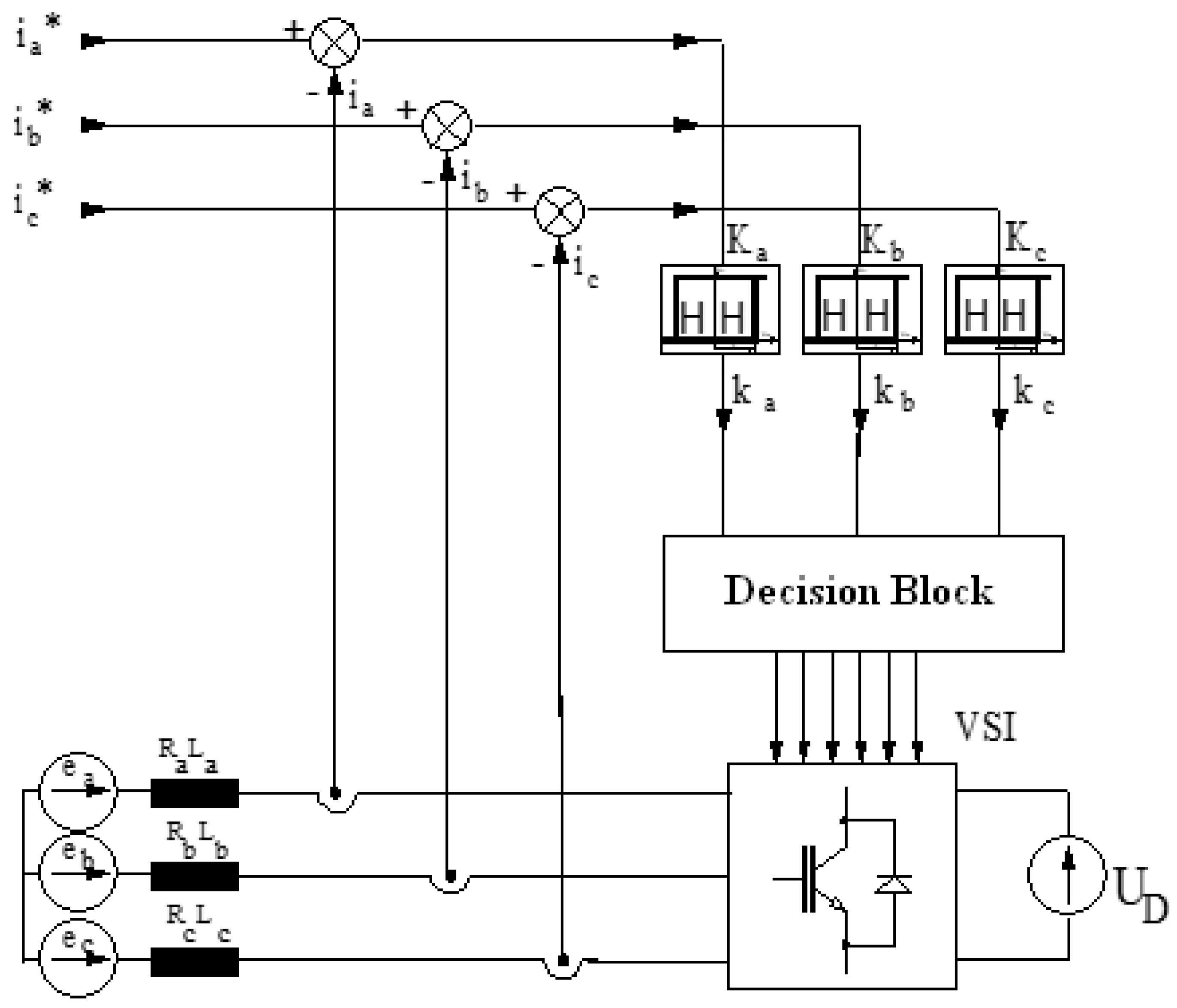
The analytical and simulation tests of the selected hysteresis algorithm used for controlling the mains converter have been carried out based on the mains converter model shown in Figure 1. Compared to the standard model of a DC/AC inverter, it differs in the structure of the intermediate circuit, in which the ideal supply voltage source is replaced by capacitance C and the current generator G is the source of current with the value and direction determined by the converter load. The internal conductivity of the generator is assumed to be equal to zero. The intermediate circuit voltage is equal to the voltage on the condenser. The switching states in individual phase branches of the converter are changed by three ideal keys .
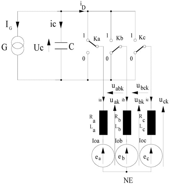
Figure 1.
Model of PWM mains converter.
On the supply network side, there are three phase chokes with inductances and resistances . The voltages are the phase voltages of the network, while the voltages stand for the interphase voltages. Then, the voltages and are, respectively, the phase and interphase voltages at output terminals of the converter. The symbols represent the values of phase currents at a selected time . The directions of the currents and voltages shown in the figure are considered positive. The indexes a, b, and c refer to phases A, B, and C, respectively, while the index k is the number of the activated vector. For the switching status shown in Figure 1, the index k is equal to 4 in the decimal number system or to 100 in the binary number system. In accordance with the adopted model, the index k can take 8 values, 0, 1, 2, 3, 4, 5, 6, and 7, in the decimal number system, which correspond to subsequent switching states of the converter, referred to as vectors and marked .
In the adopted model of the converter, the equation for phase a has the form (1).
Then, the equation describing the model of an ideal converter can be written as a matrix equation in the form corresponding to the notation of phase Equations (2) and (3).
The matrix I in Equation (3) is the transposed matrix of phase currents (4).
ZL is the inductance matrix (5).
R is the resistance matrix (6),
and E is the transposed voltage matrix (7).
The interphase voltages uabk and ubck and phase voltages uak, ubk, and uck of the converter are calculated from voltage UD = UC and take the values shown in Table 1 and Table 2.

Table 1.
Interphase voltages for individual vectors .
Table 2.
Converter output voltages for individual vectors .
The voltage is calculated from the intermediate circuit Equation (8).
The intermediate circuit current depending on the activated vector, , is calculated from the measured phase currents and and take the values shown in Table 3.
Table 3.
Interphase voltages for individual vectors .
The R, L, and RMF circuit of the converter model is described by the system of Equations (9).
The time interval between the activation times of subsequent vectors and is considered. It is assumed that during the action of vector , the electromotive forces are constant and equal to , respectively. Solving the equation system leads to the analytical expression describing the phase current waveforms (10).
The initial phase currents are given in the form (11),
while the electromotive forces have the values (12),
where means the phase shift angle between the set current and the electromotive force of the given phase.
Equation (10) remains valid in the time interval in which the vector is activated. This time is not constant, in general, and after activating the next vector at time , new values of electromotive forces and initial currents (13)
should be introduced to the current waveform formulas.
The interphase voltages and appearing in Equations (9) and (10) and the resulting phase voltages , , and at converter output are given in Table 1 and Table 2. The values of these voltages depend directly on the supply voltage . Table 2 also includes the zero-point potential related to the negative-pole potential () of the power rail.
The recursive procedure for determining the phase current waveforms in the converter model is reduced to attributing phase voltages given in Table 2 to subsequent vectors . According to (10), for the sequence of vectors activated at times , respectively, the formula describing the current waveform for phase a has the form (14),
where the voltage , the electromotive force , and the initial current have values depending on the activated vector For instance, at time , the initial current and the electromotive force of phase a reach the values given by (12) and (14), respectively.
The formulas describing the waveforms of phase currents are valid for the presented model of the mains converter. In particular, provided that the adopted assumptions are maintained, they are valid after activating one vector assuming that in the set time interval the source voltages of the supply line are constant. Adopting the above assumptions results from the fact that the time interval is shorter by at least two orders of magnitude than the time constant of the load circuit and the period of the power supply network. Therefore, we can assume that the phase current waveform in the assumed time interval is linear, and that Equation (10) describing these waveforms can be simplified, thus accelerating their digital processing. The time derivative of phase current (10) has the form (15)
and its value at time is equal to (16).
Therefore, the instantaneous phase current waveform can be approximated by Equation (17),
and Equation (10) can be replaced by linearised expression (18).
During the simulation and experimental tests conducted in the Institute of Electrical Engineering, the results were compared for the cases in which control algorithms were based on Equation (10) with those making use of the linearised Equation (14). The obtained results turned out to be very close to each other, and the differences between the waveforms of corresponding currents and voltages were negligibly small.
2.2. Converter Control Algorithm
Based on the adopted model of the converter, simulation tests were carried out for five selected control algorithms, labelled as A1, A2, A3, A4, and A5.
The properties of individual algorithms were compared using the following parameters:
| h | content factor of output current harmonics |
| minimal time between switches of inverter terminals | |
| maximal time between switches of inverter terminals | |
| Tśr | average time between switches |
| vnum | number of vector switches in one period of current |
| average value of the DC voltage source current | |
| amplitude of the set current value | |
| I | RMS value of the phase current |
| H | width of the current control error hysteresis zone |
| SH | width of the auxiliary current control hysteresis zone |
| frequency of the fundamental harmonic of the set inverter current | |
| period of the fundamental harmonic of the set inverter output current | |
| frequency of digital sampling of the inverter control system | |
| period of digital sampling of the inverter control system | |
| intermediate circuit voltage | |
| load circuit reactance | |
| load circuit resistance | |
| phase shift between the current waveform and the electromotive force |
The comparison tests were carried out for the converter load in the form of the rotor circuit model of an asynchronous ring machine with a double-sided power supply.
The parameters of the equivalent diagram of the machine are as follows:
- -
- The machine rotor circuit: ,
- -
- The set waveform of rotor current
- -
- -
- The electromotive force
The following assumptions were made for the simulation tests:
- -
- Converter supply voltage
- -
- cos;
- -
- Current waveform hysteresis zone: H = 20 A;
- -
- Auxiliary hysteresis zone: SH = 10 A.
2.2.1. Structure of Control Systems
Given below is a brief description of the studied control algorithms and block diagrams of systems implementing them.
A1. Hysteresis algorithm with analog comparators
The object of tests was the control system shown in Figure 2. The error is defined as the difference between the set current and the measured current (19).

Figure 2.
Control system with three analog error comparators.
The phase error signals are given to the inputs of the analog comparators with hysteresis characteristics. In all three phases, the hysteresis zone has the identical value H. At the outputs of the comparators, digital signals are obtained, to whom state 1 or state 0 is attributed depending on their level. A control variable in the form of a binary number is constructed from these signals. Based on this variable, the decision block selects an inverter vector according to principle , where k is a decimal number with the value corresponding to the binary number . In the stationary coordinate system α-jβ, the 3D inverter output voltage vector assigned to this number has the form (20),
where is the position angle coefficient of vector relative to the coordinate system α-jβ. It is usually assumed that the direction of vector is consistent with the axis of real component, and then the coefficient is assigned to the next vector k according to Table 4.
Table 4.
Coefficients of vectors .
Thus, the selection of vector depends on the location of the current error vector in the complex plane sector determined by the control variable. For two control variable states, (000) and (111), the zero output voltage vector is activated.
Algorithm A1 does not introduce restrictions on the inverter switching speed. However, taking into account the capabilities of the simulation program, discretisation of the control process was introduced, which consisted in sampling the current with a maximum frequency of 1 MHz. In real systems, analog comparators can change the initial state in the time below 1 µs, and the applied simulation model does not reproduce this property well. However, compared to object parameters, the assumed sampling period can be considered sufficiently short and the results obtained in this way reliable.
A2. Hysteresis algorithm with comparators activated periodically
The object of the simulation was the control system shown in Figure 3. The converter is controlled according to the hysteresis algorithm based on the solution of Algorithm A1. However, the error signals are activated here with constant frequency at the inputs of the analog comparators. The sampling period is selected taking into account dynamic properties of the object to avoid excessively high inverter switching frequencies. The algorithm was tested for the time = 100 µs. In the other solution, the control variable can be activated periodically at the decision block input, as shown in Figure 3, while the phase currents are measured continuously. This model was selected for further studies. Vector is selected following the same principle as for Algorithm A1.
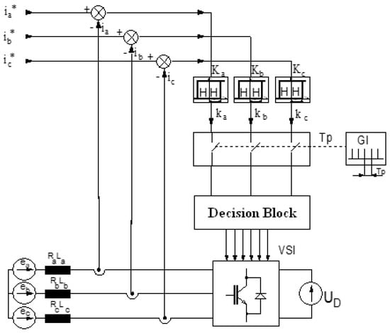
Figure 3.
Control system with three error comparators activated periodically.
It is noteworthy that for the assumed sampling frequency, there is a limit to hysteresis zone reduction. Exceeding this limit worsens, not improves, the inverter operation, as the load current is changing too fast and exceeds the error zone boundary before inverter switching is allowed. The rate of current changes is determined by the time constant of the load circuit. It is obvious that the hysteresis zone width should be properly correlated with the sampling frequency and load circuit parameters to obtain correct operation of this algorithm.
A3. Hysteresis algorithm with two error comparators
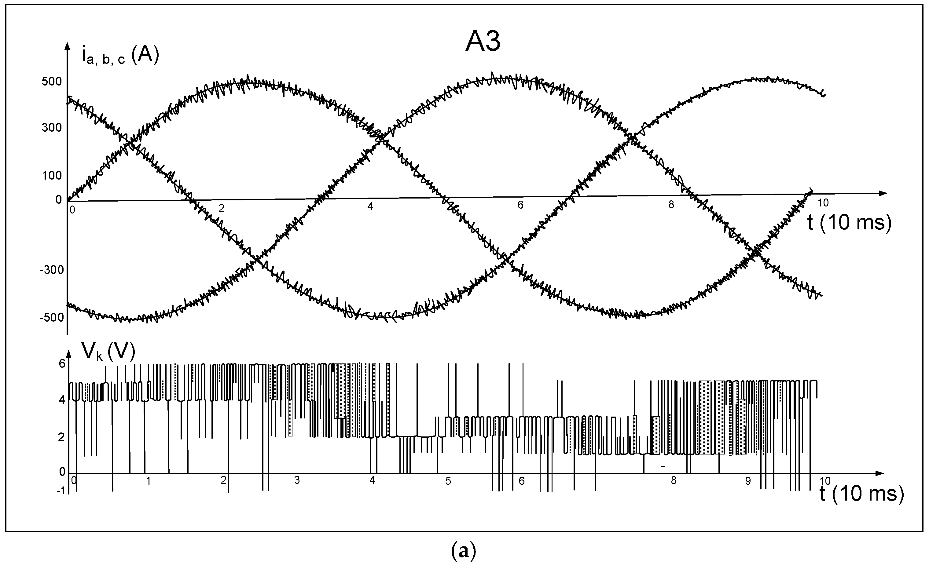
An example of the implementation of the hysteresis algorithm with two error comparators in each phase is the solution presented in [20]. The decision algorithm is saved in EPROM memory as a set of numbers corresponding to individual inverter vectors. Selecting a specific vector consists in reading the selected memory cell, i.e., passing the address of this cell. This address is constructed from standard output signals from analog comparators.
Compared to the control system operating according to Algorithm A1, the system implementing the algorithm with two comparators was expanded to include a group of additional auxiliary comparators SKa, SKb, and SKc. The decision block receives six digital control signals, based on which it determines the required states of inverter switches. Introducing these additional comparators, with smaller hysteresis zone SH, makes the information about the status of errors in all three phases become more complete. The basic comparators control the activation of active vectors, while the auxiliary comparators are used for the activation of zero vectors. This principle was used in tests of Algorithm A3, the operation of which is shown in Figure 4. Compared to the algorithm presented in [20], there is an important modification here—periodic activation of comparators has been introduced to Algorithm A3. It was assumed that the hysteresis zone SH of auxiliary comparators is equal to 50% of zone H.
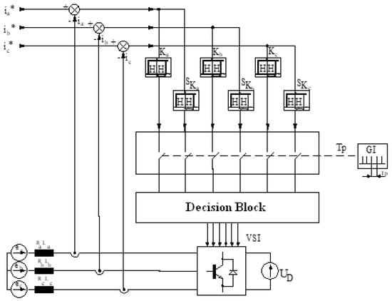
Figure 4.
Control system for Algorithm A3 implementation.
A4. Hysteresis algorithm with sampling
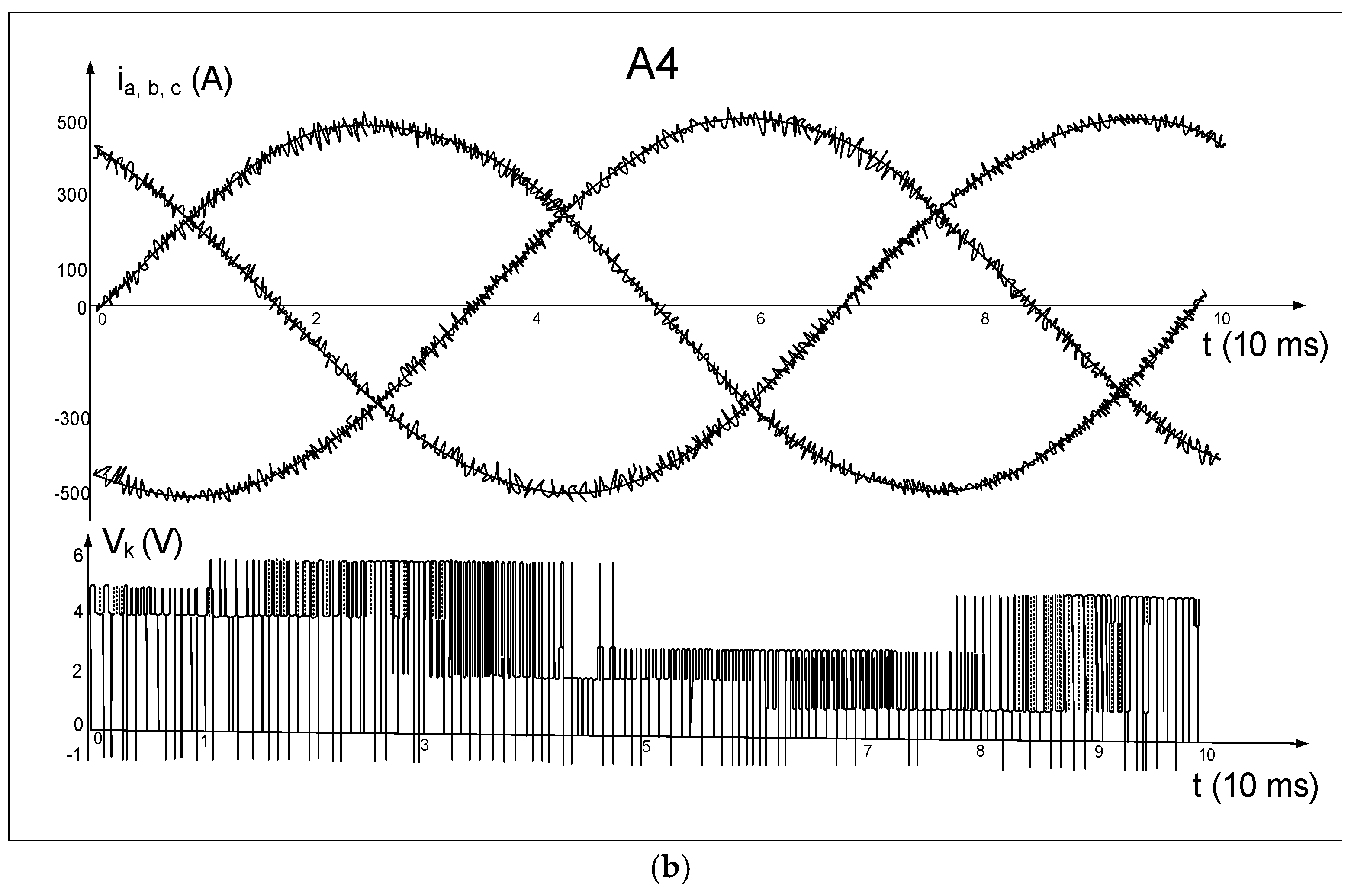
This algorithm is a variation of a type of control algorithm called delta modulation algorithms. The principle of operation of this algorithm is based on a concept proposed in [35]. This algorithm has two important features. The first of them is the principle of periodic sampling of phase currents, and the second is the tendency to activate zero vectors as often as possible.
The phase current error is compared with the set error zone H, after which the following decision-making procedure is executed:
- -
- If > H then the non-zero vector is activated;
- -
- If < H then the zero vector is activated.
Non-zero vectors are activated when the error signal exceeds the set zone corresponding to the activation of zero vectors. This means that as soon as the error returns to this zone, the zero vector is activated in the first subsequent sampling cycle. The algorithm selects a zero vector whose activation requires a smaller number of switches.
A5. Hysteresis algorithm selecting a vector with the longest operation
This algorithm was based on the concept of selecting the inverter output voltage vector with the longest operating time [36]. In this algorithm, the selection of vectors takes place first to reject vectors useless for control at a given phase current error status. Then, after calculating the operating times of the pre-selected vectors with “good direction”, the best of them is chosen. The criterion here is the maximum time of staying of the current error vector within the permissible error area. This area has a form of a regular hexagon with a side’s length equal to H.
Preliminary selection of vectors consists in determining the vector corresponding to the location of the current error vector in a specific sector of the complex plane (as for Algorithm A1), with further qualification of the neighbouring vectors and the zero vector.
In the phase of operating time calculation for the qualified vectors, the load model described by the equations presented above is used.
2.2.2. Results of Simulation Tests of Selected Hysteresis Algorithms
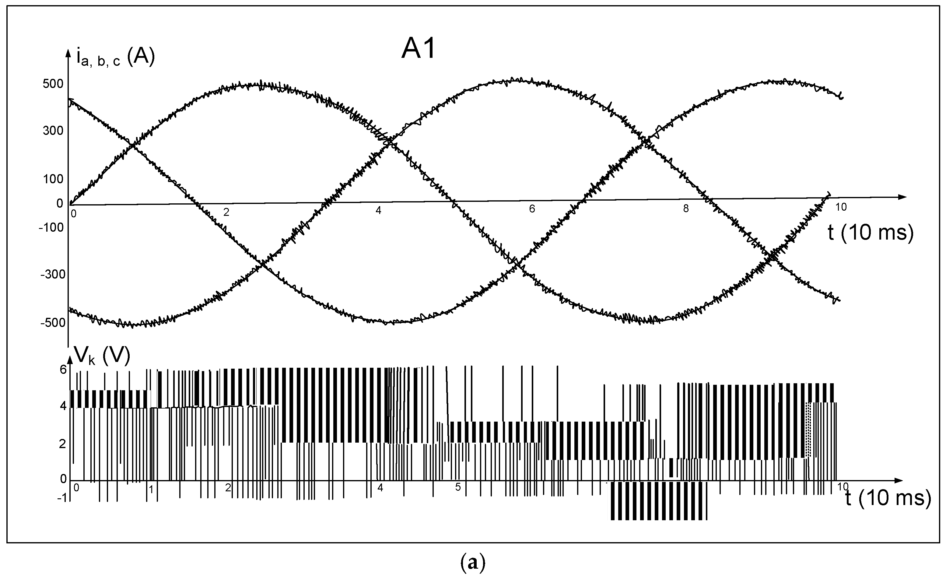
Figure 5, Figure 6 and Figure 7 show printed waveforms of inverter phase currents and voltage vectors obtained in simulation tests of individual algorithms. The simulation runs of hysteresis Algorithms A1 and A2 are shown in Figure 5, Algorithms A3 and A4 in Figure 6, and Algorithm A5 in Figure 7. These simulations were obtained for the following assumed values of simulation model parameters:
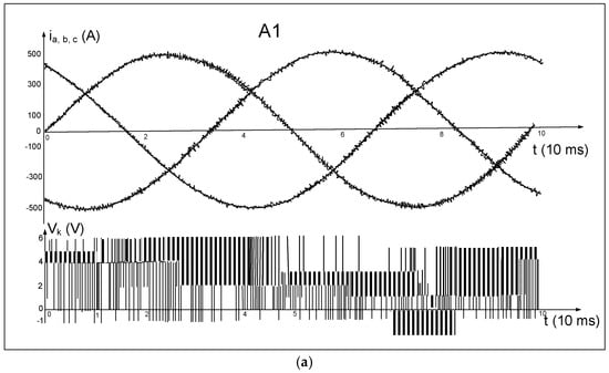
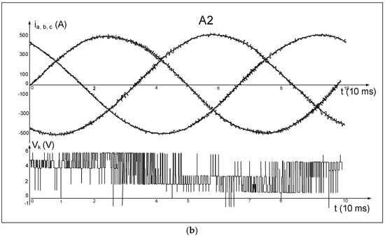
Figure 5.
Waveforms of inverter phase currents and voltage vectors for hysteresis Algorithms A1 (a) and A2 (b).


Figure 6.
Waveforms of inverter phase currents and voltage vectors for hysteresis Algorithms A3 (a) and A4 (b).
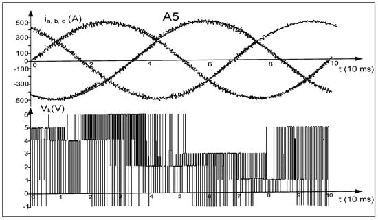
Figure 7.
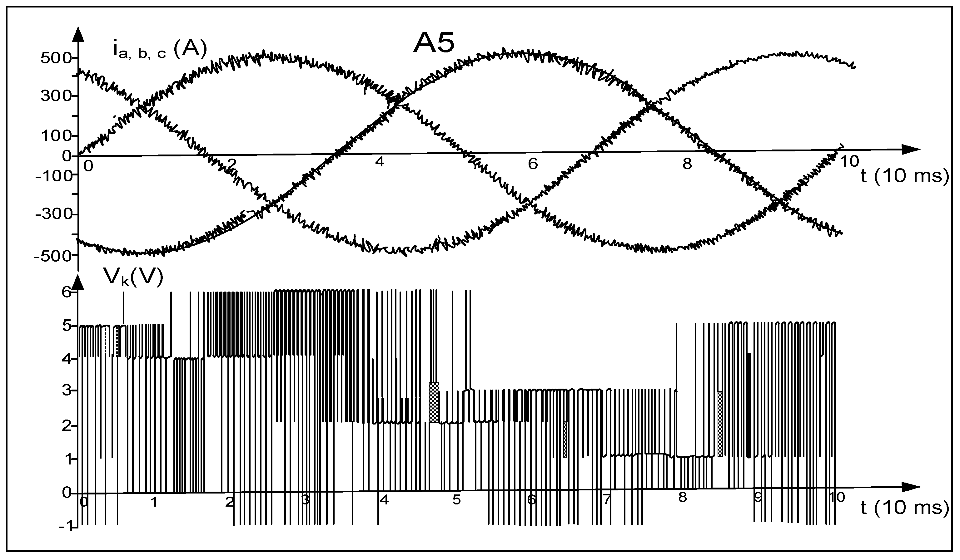
Waveforms of inverter phase currents and voltage vectors for hysteresis Algorithm A5.
The three next figures, Figure 8, Figure 9 and Figure 10, show selected examples characterising the properties of the hysteresis algorithms. These results were obtained for different parameters of the control model.
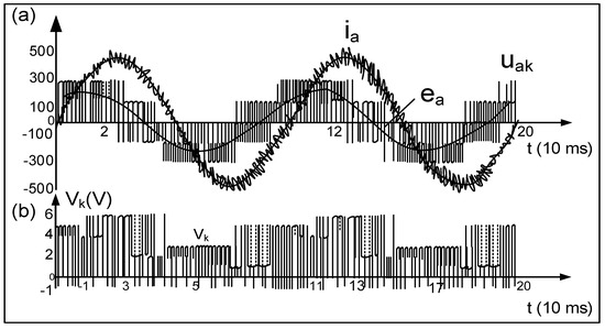
Figure 8.
Phase current ia, electromotive force ea, inverter output phase voltage Uak (a), and inverter voltage vectors Vk, (b) obtained for the control model according to the discretized Algorithm A5; the assumed sampling period Tp = 100 µs. (Zero vectors Vk = 7(111) marked with number −1).

Figure 9.
Illustration of dynamic properties of the inverter controlled according to the hysteresis Algorithm A1 based on the phase current waveforms obtained at step change of the set value of the current (a), inverter voltage vectors Vk, (b) (zero vectors Vk = 7(111) marked with number −1).
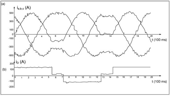
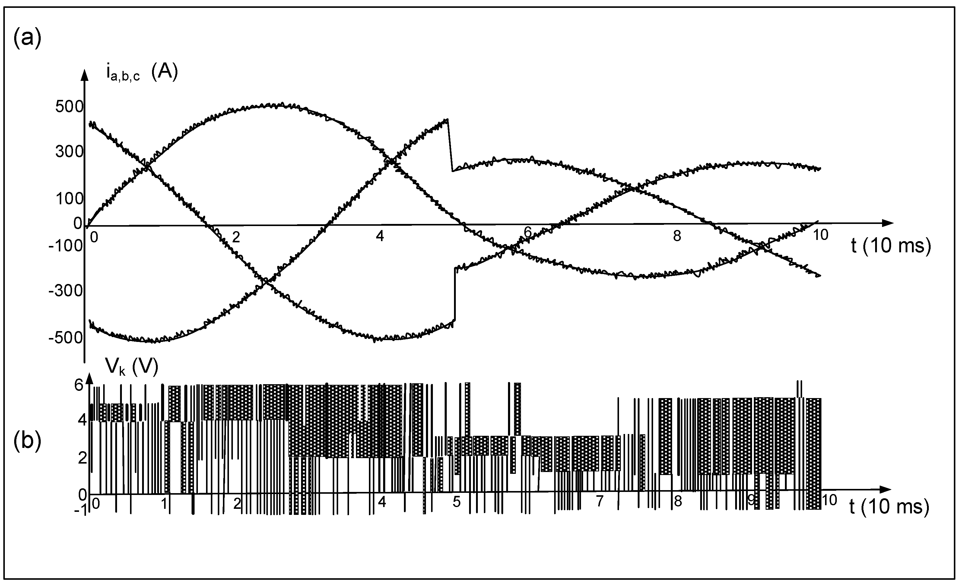
Figure 10.
Three modes of converter operation are controlled according to Algorithm A5: inverter operation, synchronous operation (the set current frequency f = 0), and rectifier operation: (a) three-phase currents, (b) average current value iD.
Figure 10 shows the situation simulated during the tests of the shaft generator control system. The curves shown represent the machine converter phase current waveforms. The set current frequency was equal to f = 1 Hz. Initially, the generator operates at sub-synchronous speed, which makes the converter work as an inverter, supplying AC power to the machine rotor. The average current value is positive, as the energy is taken from the intermediate circuit. Then, the printout shows the synchronous operation mode and transition to the mode of super synchronous operation of the generator. In the synchronous mode, the converter continues to operate as an inverter, providing energy to cover resistive losses, while the super synchronous operation of the generator is characterized by transferring part of the energy to the rotor circuit, as a result of which the converter switches to the rectifier operation mode. The next operation modes shown on the printout represent (again) the synchronous operation and return to the sub-synchronous operation. The visible irregularities in the waveform of the average current iD result from the low accuracy of software averaging.
2.2.3. Evaluating Results of Simulation Tests
The results obtained in the simulation tests are summarised in Table 5. It is noteworthy that the parameter vnum included in the table determines the number of converter vector switches. The simulation programincreases this number at each vector change. This number is not equal to the number of terminal switches, as converter switches many occur in which more than one terminal changes state.
Table 5.
Results of simulation tests of algorithms.
The obtained simulation results allow the determination of basic properties of the control making use of hysteresis algorithms.
The simplicity in implementation of Algorithm A1 is accompanied by good control properties. The algorithm ensures that the current flow is kept within the set limits. It also provides high-speed response to the step change of the set current value. The basic disadvantage of Algorithm A1, which eliminates the possibility of its use for controlling the operation of higher-power converters, is the instability of the inverter switching frequency. Very short time intervals between switches may occur, which are beyond physical switching capabilities of the presently used power semiconductor elements. Moreover, quick switches contribute to the increase in the content of higher harmonics in the output current.
The other way to protect against the high switching frequency of converter terminals consists of periodic testing of phase current errors. This method was applied in Algorithm A2. As a result, this algorithm does not allow such quick switches as Algorithm 1. The converter switching becomes more uniform, and the value of the coefficient vnum decreases. Compared to Algorithm A1, all remaining algorithms have a much smaller Tmax/Tmin ratio. In this respect, Algorithms A3 and A5 look most beneficial. However, Algorithm A3 requires a relatively large number of switches, which is most likely related to the obligatory zero vector activation in the zone of auxiliary comparators, without checking the direction of RMF.
In all three Algorithms, A2, A3, and A4, the assumed current sampling frequency fp = 10 kHz determines the minimum time Tmin = 100 s between switches.
For Algorithm A5, which, similarly to algorithm A1, allows switching with maximum frequency fp = 1 MHz, the ratio = Tmax/Tmin takes a value close to that obtained for periodic Algorithms A2 and A4. At the same time, with relatively little variation in switching times, the total number of all switches is larger than for Algorithms A2 and A4, which results from allowing for the appearance of switches not synchronized by the sampling frequency.
Comparing the currents ID taken from the power source we can see that they do not differ significantly for individual algorithms. The smallest current ID occurs during control according to Algorithms A5 and A1, while the largest is taken during control according to Algorithm A2.
The uniformity of phase currents, determined by comparing their RMS values, is similar for all algorithms. The lowest value of the higher harmonic content coefficient h in output currents occurs during control according to Algorithms A1 and A5, which results from the fact that these algorithms are aperiodic, with the ability to switch with an accuracy of up to 1 s.
Only the two aperiodic algorithms ensure keeping the current accurately within the set error zone. If a switching speed limit is introduced to Algorithm A5, then achieving such an accuracy becomes impossible. The performed tests have also shown that Algorithm A5, at a relatively small number of switches, improves the regularity of converter switching, which is confirmed by the uniformity of loads of individual semiconductor switches, at a much smaller ratio ϑ = / compared to Algorithm A1.
2.2.4. Experimental Tests of Hysteresis Algorithms
The results obtained in simulation tests have been verified practically. The experimental tests were performed on a laboratory model of the system shown in Figure 11. In the first stage, the object of control was the squirrel cage motor SZJCe 563 6.1 kW and then an asynchronous ring motor with a power of 50 kW.
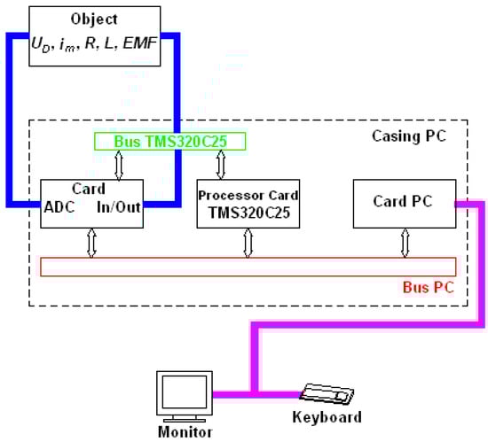
Figure 11.
System for experimental tests.
The tested object was equipped with 7 measuring transducers with analog output signals. Two of them were used to measure currents in the rotor, two for currents in the stator, two for stator voltage, and one for voltage on the DC circuit capacitor. Additionally, digital signals were obtained from the rotational speed encoder installed on the object.
The algorithms to be tested were implemented into the control system, the central unit of which was a fixed-point signal processor. For this purpose, the Texas Instruments processor TMS320C25 was selected. The control system consisted of the DSPrime 25/32 (APRO SA) card with a signal processor and a card with analog-to-digital converters and input–output systems placed in the IBM PC station. The access to these two cards was via the computer bus. The communication between the converter cart and the processor card was via a high-speed signal processor bus. The current waveforms were read online and displayed on the monitor screen using a specially developed monitoring program which processed the data from the analog-to-digital converters.
The tests were performed with four hysteresis Algorithms: A1, A2, A3, and A4. The results of these tests, in the form of real waveforms of phase currents and inverter voltage vectors, are presented further down.
3. Rectifier and Inverter Operation of Mains Converter
In the mains converter, the energy flow is controlled by setting the phase shift angle between the network voltage and the set current waveform . The level of active and reactive power can be controlled in this way depending on needs. If work with = ±1 is required, then the angle should be adjusted accordingly to 0 or 180°, depending on the selected operating mode.
3.1. Simulation Tests of the Converter
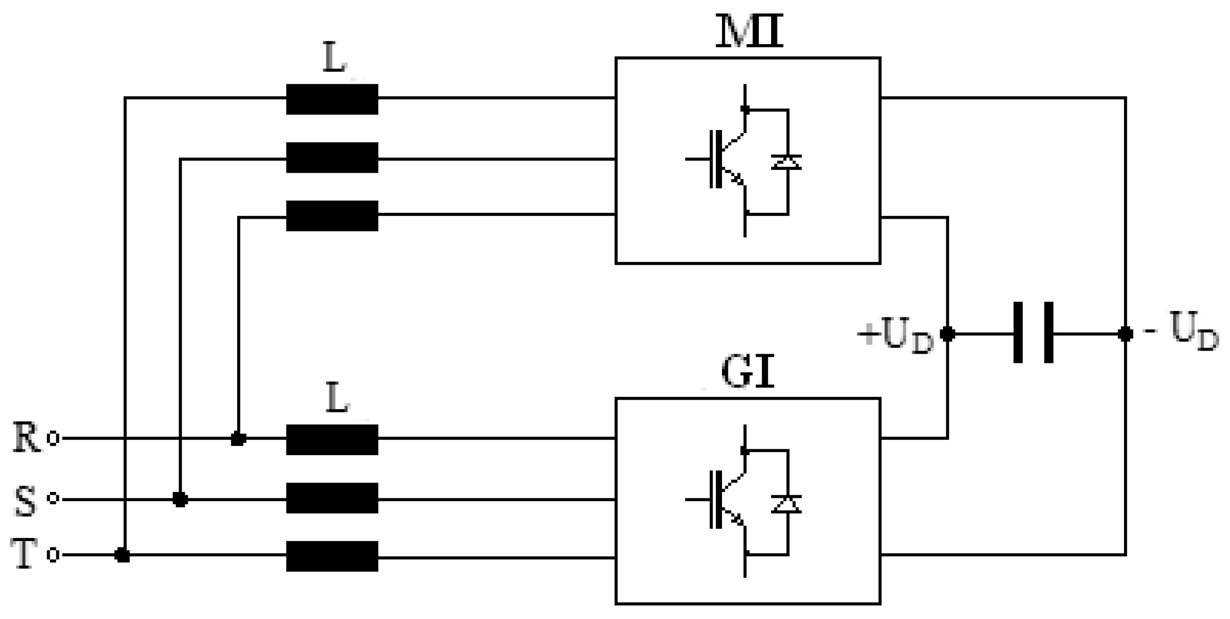
The simulation tests were performed with the model of an indirect AC-DC-AC converter, the two-component converters of which were connected to the network in the way shown in Figure 12. The AC-DC mains converter supplies energy to the load in the form of a DC-AC machine converter with three phase chokes connected to the network. The AC-DC-AC converter configured in this way could be used, for instance, as a reactive power compensator (1).

Figure 12.
AC-DC-AC converter connected to the network.
Figure 13 and Figure 14 show the results of the simulation of the two operating modes of the mains converter. It was assumed that the supply voltage on the DC side is constant. This converter, working as a voltage inverter, was controlled using the algorithm for maintaining the set current in the following form: .
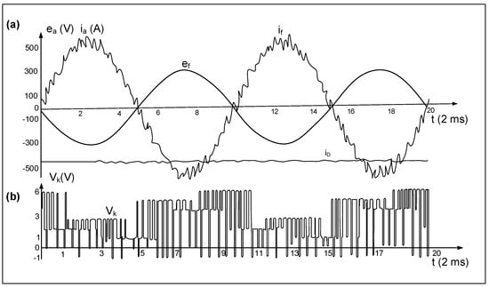
Figure 13.
Illustration of rectifier operation of the mains converter controlled according to the hysteresis algorithm: waveforms of phase currents if, the average value of intermediate circuit current iD, network voltage ef (a), and vector Vk (b).
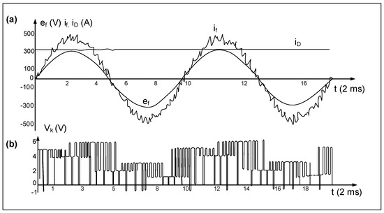
Figure 14.
Illustration of inverter operation of the mains converter controlled according to the hysteresis algorithm: waveforms of phase currents if, average value of intermediate circuit current iD, network voltage (a), and vector (b).
The next figures, Figure 15 and Figure 16, show the results of simulation control tests for the model of the intermediate AC-DC-AC converter according to Figure 14. The tests were performed based on the mains converter model shown in Figure 1.
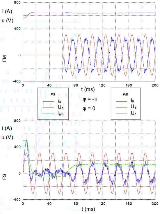
Figure 15.
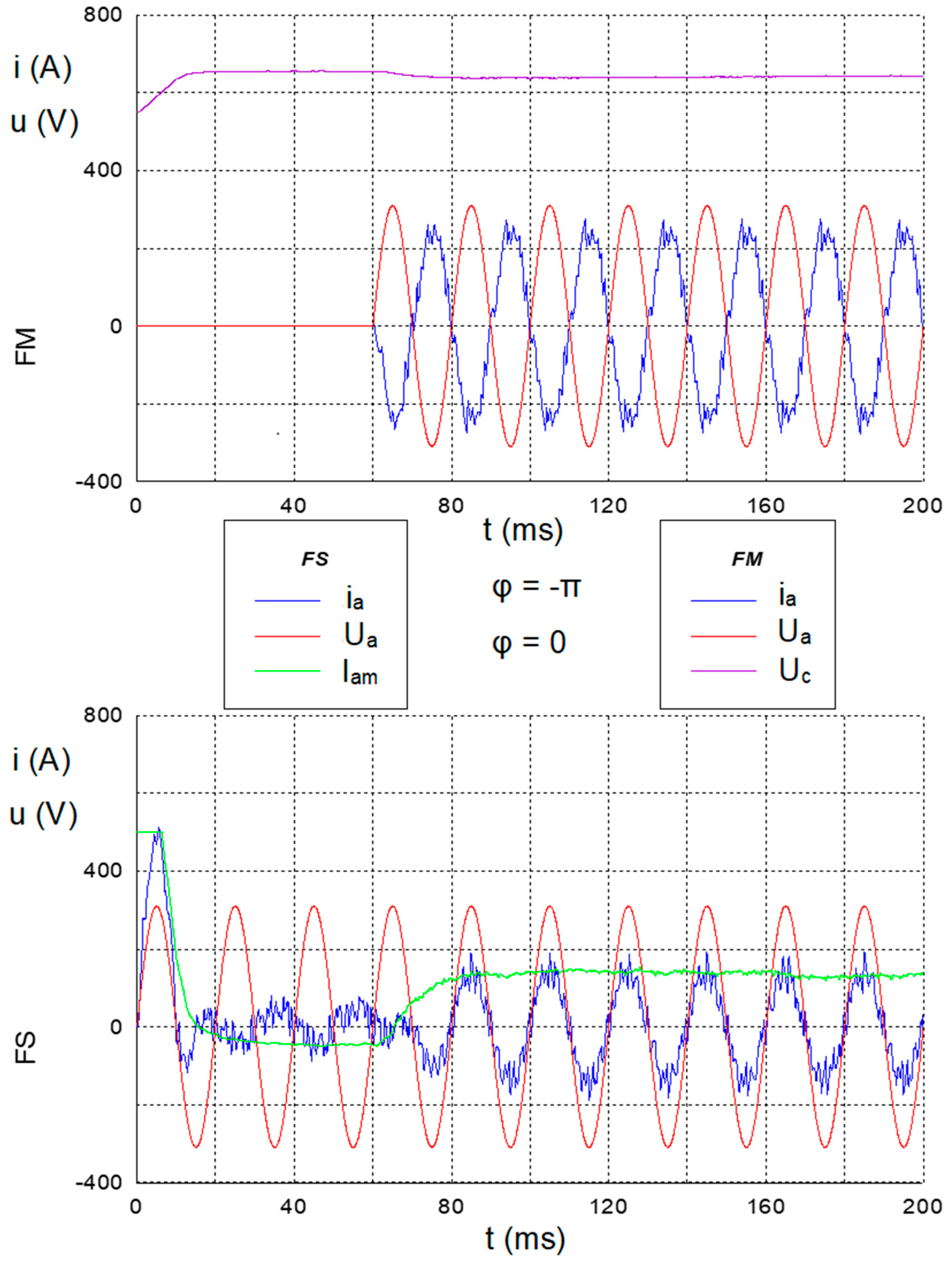
Simulated waveforms of AC-DC-AC converter: MR converter works as a rectifier, while MI converter as an inverter. For both converters, the power factor |cosφ| = 1.
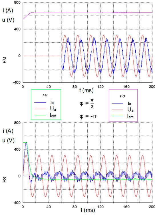
Figure 16.
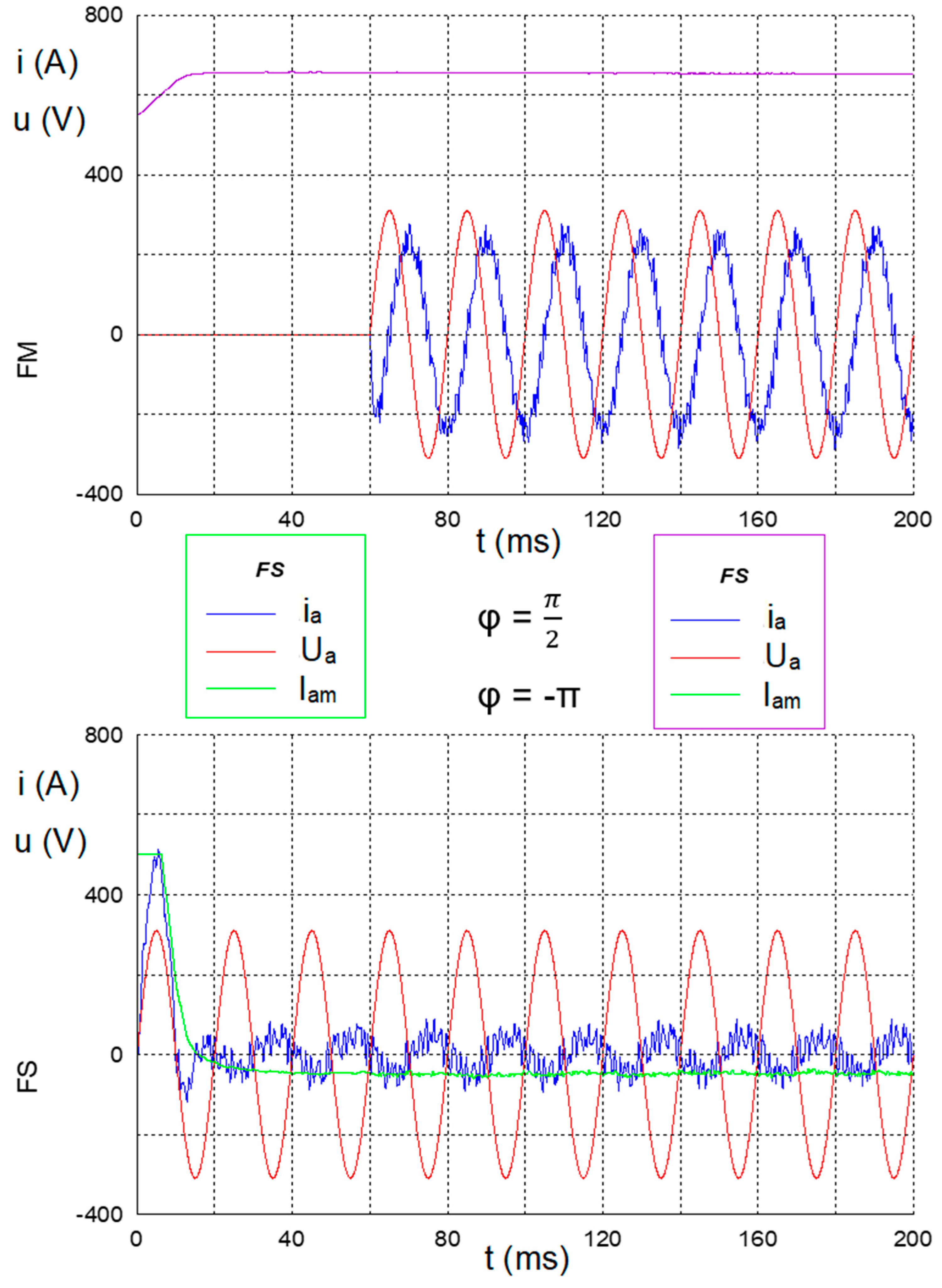
Simulated waveforms of AC-DC-AC converter in situation when the machine converter FM works as an inverter with phase shift ϕ = π/2.
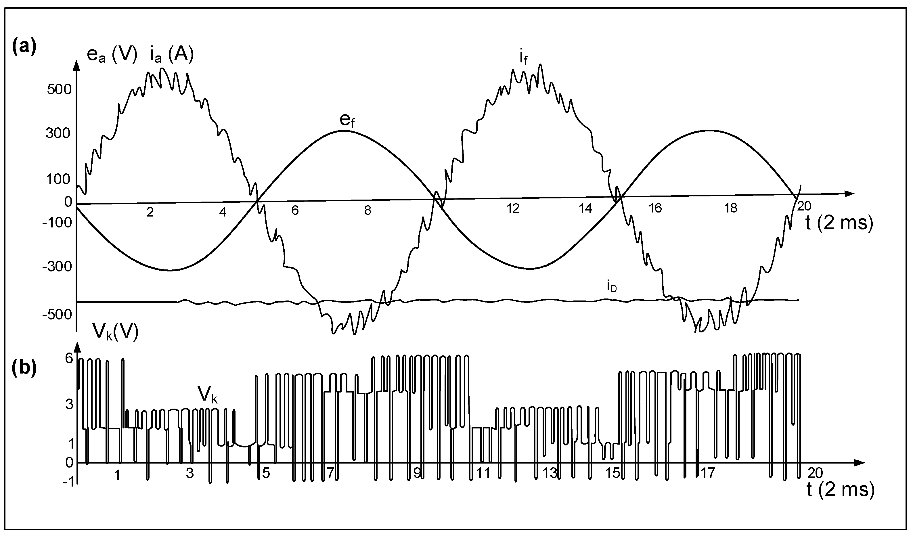
Figure 15 shows three waveforms of the motor inverter MI, intermediate circuit voltage , phase voltage , and phase current , as well as three waveforms of the mains rectifier MR, phase voltage , phase current , and intermediate circuit current. After connecting the AC-DC-AC converter to the network, the voltage on the intermediate circuit capacitor is established and both converters are ready for operation. At time , the control of the MI converter is activated, and the converter switches to the inverter operation mode. The electricity is transferred to the network, the voltage decreases due to the load on the intermediate circuit, and the shape of the phase current waveform results from the action of the applied hysteresis algorithm. The fundamental harmonic of the current is in phase with the network: . The next three runs illustrate the operation of the MR converter, which works in rectifier mode. Activated at time , the converter takes the energy from the network to charge the intermediate circuit capacitor unit to the set voltage . The charging process is very fast, and after several milliseconds the voltage reaches the set value. However, the current taken from the network during this process reaches a high value. After charging the intermediate circuit, the current decreases significantly to reach the level corresponding to the load introduced by the AC-DC-AC converter in idle condition. After activating the MI converter, the value of the current taken from the network increases as a function of the given load. According to the direction adopted in the model, the waveform of the intermediate circuit current (green graph), shows the maximum value of the direct current delivered to the intermediate circuit of the AC-DC-AC converter by the MR converter working in rectifier mode.
Figure 16 shows the same three waveforms of the motor inverter MI, , , and three waveforms of the mains rectifier MR, , , but in a situation when the machine converter does not load the intermediate circuit. Like in the previous case, the MR converter activated at time quickly increases the voltage on the intermediate circuit to the value set in the control system. At time , the MI converter is activated. In this converter, the current is delayed with respect to voltage by the angle (). This control means that the MI converter does not take active power.
3.2. Experimental Tests of Converters
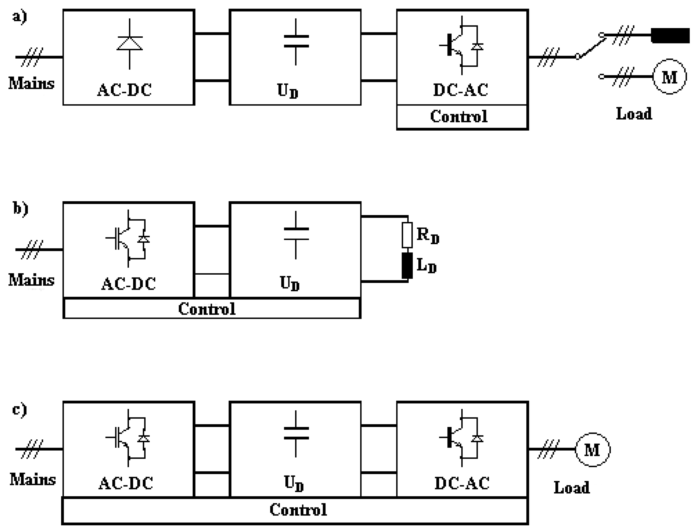
The objects of the tests were the AC-DC and DC-AC converters controlled separately. The tests were performed in the power electronics laboratory of the Institute of Electrical Engineering in Gdansk. The used laboratory model made it possible to conduct tests with converters with different structure and power not exceeding 15 kW. Three possible applications in the form of typical converter topologies, AC-DC, DC-AC, and AC-DC-AC are shown in Figure 17. The system in Figure 17a is a conventional frequency converter. In this system, only the machine converter is controlled, and the supply voltage , supplied from the rectifier, is declared as a constant parameter in the control system. Figure 17b shows the mains converter with load on the DC side, useful for rectifier work tests. Here, the control system can be equipped with the controller of the intermediate circuit voltage . The structure shown in Figure 17c is a complete intermediate AC-DC-AC converter. In this case, each converter is controlled by its own control card.
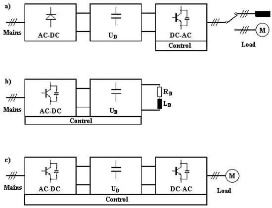
Figure 17.
Three converter structures of the laboratory model used for experimental tests: (a) frequency converter, (b) mains converter, (c) intermediate converter.
The tests were first performed with the mains converter. The following parameters of the tests were assumed:
Phase current and voltage:
- ;
- ;
- ;
- ;
- ;
- ;
- .
Load parameters:
- ;
- .
Hysteresis zone of the control algorithm:
- .
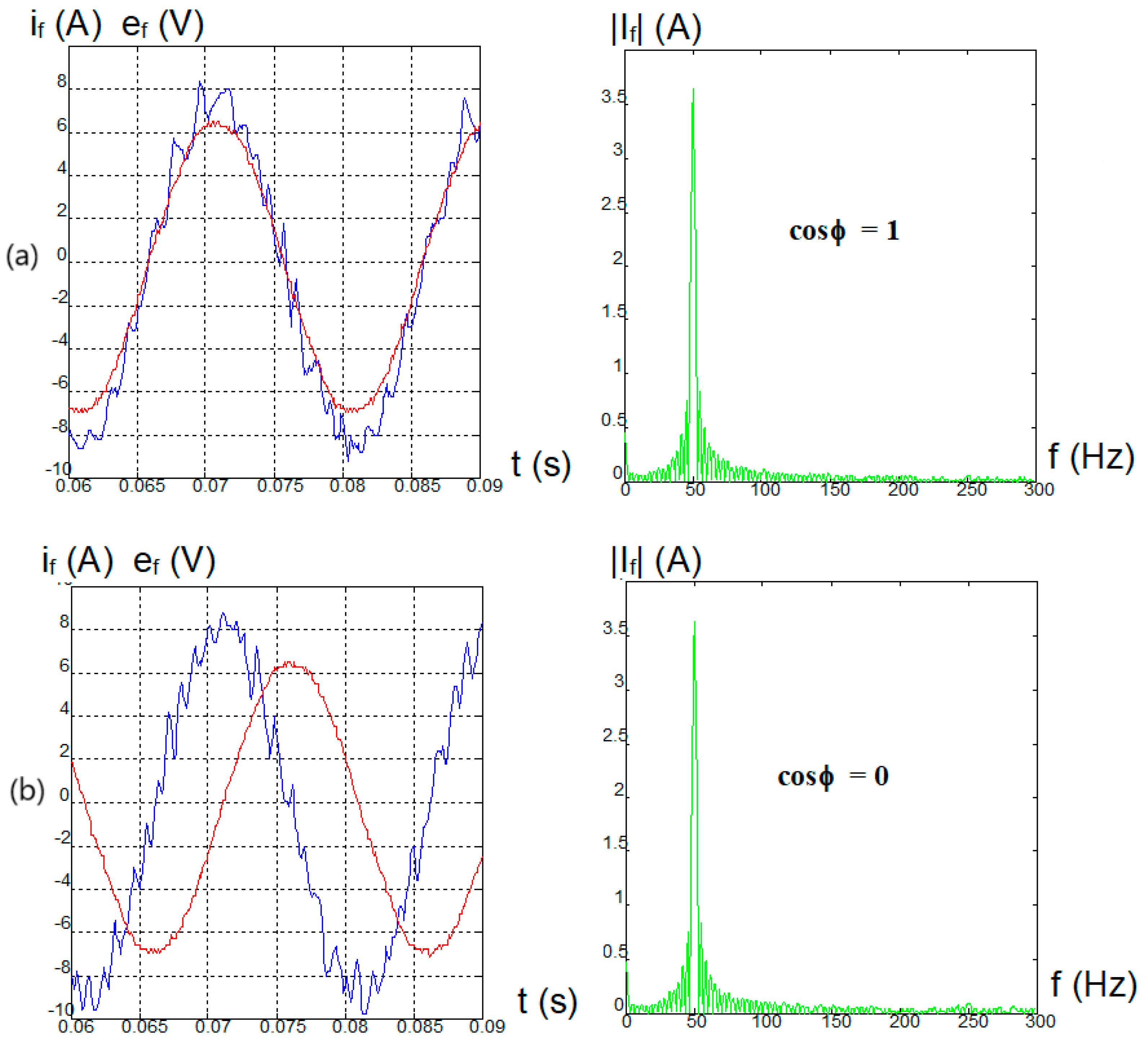
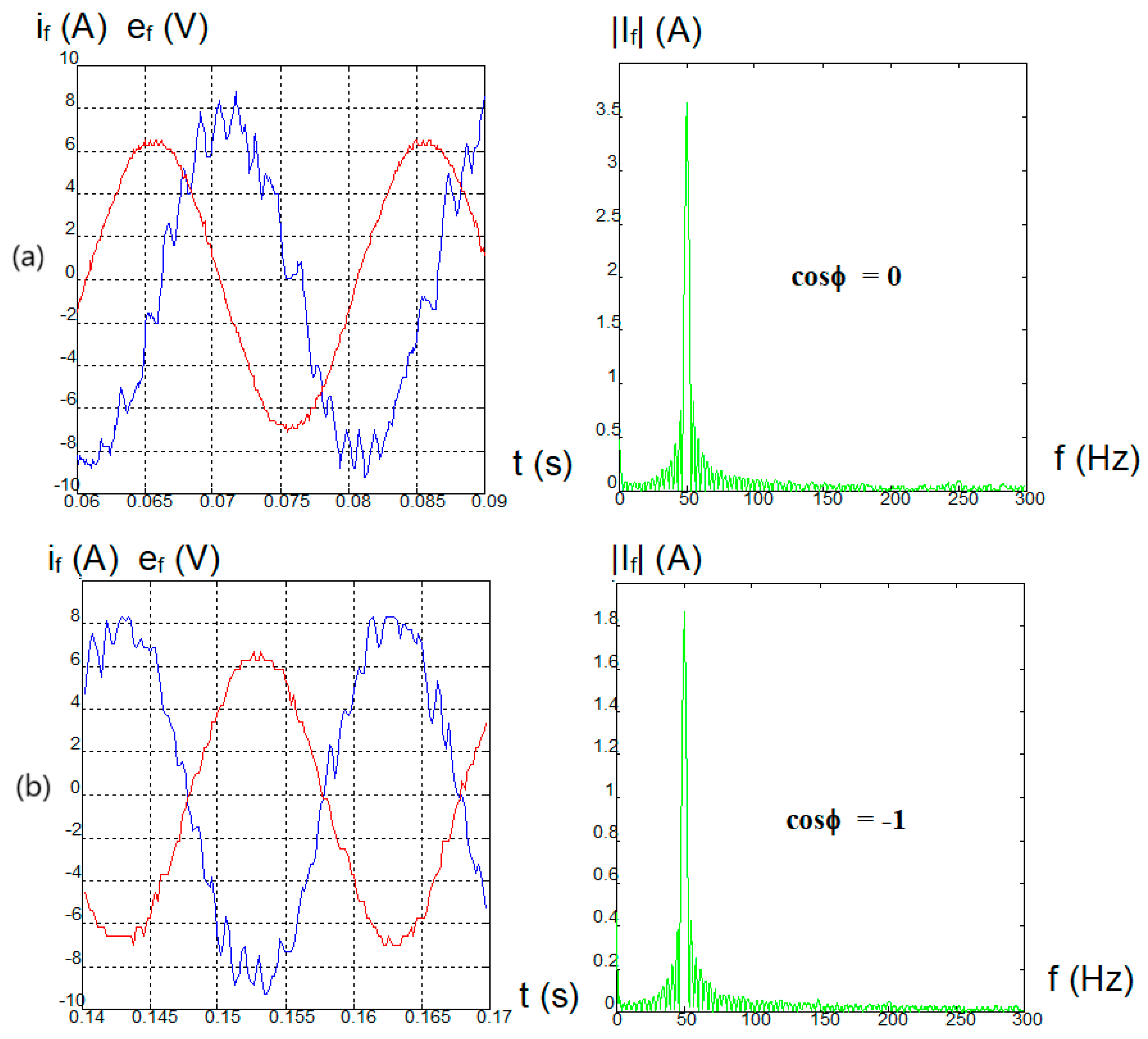
The converter was controlled using the dSpace1102 card. Control synchronization was achieved by the procedures: ds1102_p14_freq and ds1102_p14_phase. The former procedure continuously sends the period value, while the latter one ensures setting the required phase. The number of 31,250 pulses is assigned to the network period. Phase setting consists in attributing a number from the range 0 ÷ 31,250 to the variable “ϕ“. If the network frequency is 50 Hz, the phase setting accuracy is equal to 0.011°. Figure 18 and Figure 19 show characteristic waveforms of phase currents and voltages in the AC-DC converter (MR) obtained in the experimental tests. The current waveforms are accompanied by the corresponding harmonic spectrum. The values of the phase shift angle φ were set successively as equal to: 0, π/2, −π/2, π.
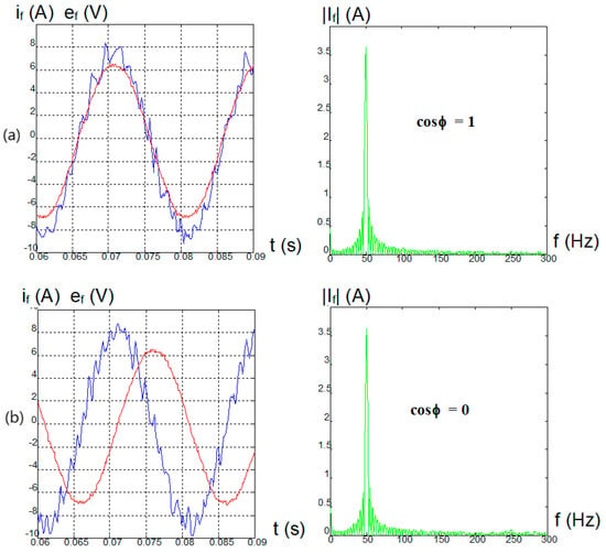
Figure 18.
Mains converter phase currents and voltages and spectrum of current harmonics for phase shift angle (a) and 0 (b).
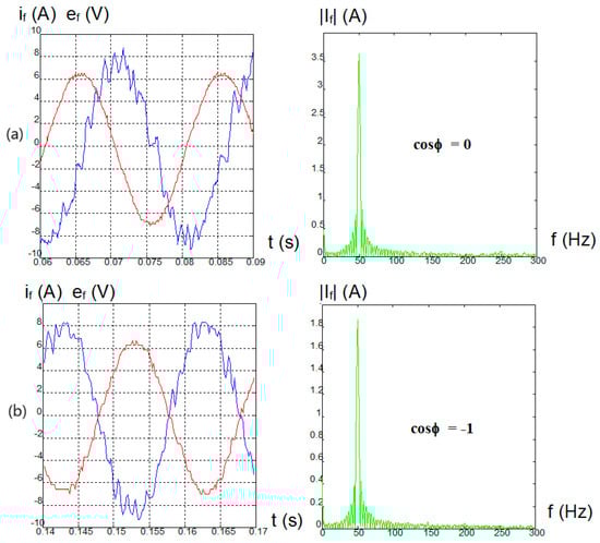
Figure 19.
Mains converter phase currents and voltages and spectrum of current harmonics for phase shift angle (a) and π (b).
In the spectra of phase current harmonics, the values of the third harmonic and the fifth harmonic are negligibly small. It can be estimated that their level does not exceed 2% of the fundamental harmonic value. For comparison, in the waveform of the input current of an inverter powered in the classic way, the third, fifth, and seventh harmonics in the spectrum can reach as much as several dozen percent of the fundamental harmonic.
The experiments were conducted with model-based control in the natural coordinate system of the hysteresis algorithm. The algorithm worked with the shortest possible processing time of the main program loop. The time interruption was set to 65 μs. In object calculations, the algorithm used a linear model, according to the equations presented in Section 2.1. For the adopted parameters of the experimental model, the number of converter switches did not exceed vnum = 50 per one period.
4. Conclusions
The AC/DC converter is capable of operating either a valuable voltage or current source of electrical energy. It depends on the applied control method. This paper presents the mathematical model of the AC/DC converter formed as a current controlled VSI. The control method makes the discussed converter operate as the current source device. The mathematical model makes it possible to define essential important physical quantity properties of the converter operating in two general modes of conversion. The analytic expressions define fundamental physical variables of the converter and their relations: phase current, voltage and reciprocal shift angle, power factor, and supply voltage. The current wave is defined as a form of short line segments while the line voltage wave is assembled from horizontal line segments forming a stepped wave in order to approximate a mathematical sine wave defining the line voltage. The lengths of steps are precisely corelated with current line segments. The use of simplified analytic expressions assures fast computer processing during simulation work.
The assumed current control method of the converter is created on the hysteresis algorithms. Five different algorithms and comparative results of their performance allow for the selection of an optimal control method depending on applications. A novel solution consisting in periodic activation of comparators has been introduced to Algorithms A2 and A3 in order to avoid excessively high inverter switching frequencies. A sampling period was selected, taking into account dynamic properties of the controlled object.
During simulation and experimental research works, the hysteresis algorithms were implemented into the control card with the digital signal processor TMS C25 Texas Instruments. A number of examples of current and voltage wave forms as well as acting vectors taken during the simulation and experimental works are executed. They proved the appropriateness and usefulness of the converter mathematical model. The proposed model seems to be a very valuable and useful mathematical tool during research works on energy conversion by use of VSIs.
Author Contributions
Conceptualization, J.I. and A.M.; methodology, J.I., A.M. and P.M.; formal analysis, J.I. and A.M.; investigation, J.I. and A.M.; writing—original draft preparation, J.I., A.M. and P.M.; supervision, J.I. All authors have read and agreed to the published version of the manuscript.
Funding
This research received no external funding.
Data Availability Statement
The original contributions presented in the study are included in the article, further inquiries can be directed to the corresponding author.
Conflicts of Interest
The authors declare no conflicts of interest.
References
- Gopi, R.R.; Sreejith, S. Converter topologies in photovoltaic applications—A review. Renew. Sustain. Energy Rev. 2018, 94, 1–14. [Google Scholar] [CrossRef]
- Donadi, A.K.; Jahnavi, W. Review of dc-dc converters in photovoltaic systems for mppt systems. Int. J. Res. Eng. Technol. 2019, 6, 1914–1918. [Google Scholar]
- Sher, H.A.; Addoweesh, K.E. Micro-inverters promising solutions in solar photovoltaics. Energy Sustain. Develop. 2012, 16, 389–400. [Google Scholar] [CrossRef]
- Alajmi, B.N.; Ahmed, K.H.; Adam, G.P.; Williams, B.W. Single-phase single-stage transformerless grid- connected PV system. IEEE Trans. Power Electron 2013, 28, 2664–2676. [Google Scholar] [CrossRef]
- Aganah, K.; Chukwuma, J.; Ndoye, M. A Review of Off-Grid Plug-and-Play Solar Power Systems: Toward a New “I Better Pass My Neighbour” Generator. In Proceedings of the 2019 IEEE PES/IAS PowerAfrica, Abuja, Nigeria, 20–23 August 2019. [Google Scholar] [CrossRef]
- Kwon, O.; Kim, K.-S.; Kwon, B.-H. Highly efficient single-stage DAB microinverter using a novel modulation strategy to minimize reactive power. IEEE J. Emerg. Sel. Top. Power Electron. 2021, 10, 544–552. [Google Scholar] [CrossRef]
- Pal, A.; Basu, K. A single-stage soft-switched isolated three-phase DC–AC converter with three-phase unfolder. IEEE Trans. Power Electron. 2020, 35, 3601–3615. [Google Scholar] [CrossRef]
- Koznowski, W.; Łebkowski, A. Analysis of Hull Shape Impact on Energy Consumption in an Electric Port Tugboat. Energies 2022, 15, 339. [Google Scholar] [CrossRef]
- Szewczyk, P.; Łebkowski, A. Studies on Energy Consumption of Electric Light Commercial Vehicle Powered by In-Wheel Drive Modules. Energies 2021, 14, 7524. [Google Scholar] [CrossRef]
- Muc, A. The three-Phase Converter with Configurable DC Input and Multilevel AC Output. In Proceedings of the 2024 IEEE 18th International Conference on Compatibility, Power Electronics and Power Engineering (CPE-POWERENG), Gdynia, Poland, 24–26 June 2024. [Google Scholar] [CrossRef]
- Liu, K.; Sheng, W.; Wang, S.; Ding, H.; Huang, J. Stability of distribution network with large-scale PV penetration under off-grid operation. In Proceedings of the International Conference on Frontiers of Energy and Environment Engineering, CFEEE 2022, Beihai, China, 16–18 December 2022. [Google Scholar]
- Xie, B.; Zhou, L.; Zheng, C.; Zhang, Q. Stability and resonance analysis and improved design of N-paralleled grid-connected PV inverters coupled due to grid impedance. In Proceedings of the 2018 IEEE Applied Power Electronics Conference and Exposition. (APEC), San Antonio, TX, USA, 4–8 March 2018; pp. 362–367. [Google Scholar]
- Fu, Q.; Du, W.; Wang, H.; Zheng, Z.; Xiao, X. Impact of the differences in VSC average model parameters on the DC voltage critical stability of an MTDC power system. IEEE Trans. Power Syst. 2022, 38, 2805–2819. [Google Scholar] [CrossRef]
- Fu, Q.; Du, W.; Wang, H.; Xiao, X. Effect of the dynamics of the MTDC power system on DC voltage oscillation stability. IEEE Trans. Power Syst. 2022, 37, 3482–3494. [Google Scholar] [CrossRef]
- Fu, Q.; Du, W.; Wang, H. Analysis of harmonic oscillations caused by grid-connected VSCs. IEEE Trans. Power Deliv. 2021, 36, 1202–1210. [Google Scholar] [CrossRef]
- Fu, Q.; Du, W.; Wang, H.; Ma, X.; Xiao, X. DC voltage oscillation stability analysis of DC-voltage-droop-controlled multi-terminal DC distribution system using reduced-order modal calculation. IEEE Trans. Smart Grid. 2022, 13, 4327–4339. [Google Scholar] [CrossRef]
- Oggier, G.G.; Jimenez, R.G.; Zhao, Y.; Balda, J.C. Modeling and characterization of 10-kV SiC Mosfet modules for medium-voltage distribution systems. In Proceedings of the 2020 IEEE 11th International Symposium on Power Electronics for Distributed Generation Systems (PEDG) (2020), Dubrovnik, Croatia, 28 September–1 October 2020; pp. 583–590. [Google Scholar]
- Edwin, F.F.; Xiao, W.; Khadkikar, V. Dynamic modeling and control of interleaved flyback module-integrated converter for PV power applications. IEEE Trans. Ind. Electron. 2013, 61, 1377–1388. [Google Scholar] [CrossRef]
- Komurcugil, H.; Bayhan, S.; Bagheri, F.; Kukrer, O.; Abu-Rub, H. Model-based current control for single-phase grid-tied quasi-Z-source inverters with virtual time constant. IEEE Trans. Ind. Electron. 2018, 65, 8277–8286. [Google Scholar] [CrossRef]
- Sulkowski, W. Modified Hysteresis Current Regulator for 3-Phase PWM-VSI. In Proceedings of the 6th Global Power, Energy and Communication Conference, Budapest, Hungary, 4–7 June 2024; 1990; Volume 2, pp. 474–478. [Google Scholar]
- Iwaszkiewicz, J. A predictive algorithm for current controlled voltage source inverter. In Proceedings of the ISIE ’93—Budapest: IEEE International Symposium on Industrial Electronics Conference, Budapest, Hungary, 1–3 June 1993; pp. 514–518. [Google Scholar]
- Nagy, I. Novel Adaptive Tolerane Band PWM for Field-Oriented Control of Induction Machines. IEEE Trans. Ind. Electron. 1994, 41, 406–417. [Google Scholar] [CrossRef]
- Rajeev, M.; Agarwal, V. Single phase current source inverter with multiloop control for transformerless grid–PV interface. IEEE Trans. Ind. Appl. 2018, 54, 2416–2424. [Google Scholar] [CrossRef]
- Mohomad, H.; Saleh, S.A.; Chang, L. Disturbance estimator-based predictive current controller for single-phase interconnected PV systems. IEEE Trans. Ind. Appl. 2017, 53, 4201–4209. [Google Scholar] [CrossRef]
- Dumitrescu, A.-M.; Griva, G.; Bojoi, R.; Bostan, V.; Magureanu, R. Design of current controllers for active power filters using naslin polynomial technique. In Proceedings of the 2007 European Conference on Power Electronics and Applications, Aalborg, Denmark, 2–5 September 2007; pp. 1–7. [Google Scholar]
- Akbar, F.; Cha, H.; Do, D.-T. CSI7: Novel Three-Phase Current-Source Inverter With Improved Reliability. IEEE Trans. Power Electron. 2021, 36, 9170–9182. [Google Scholar] [CrossRef]
- Estévez-Bén, A.A.; Tapia, H.J.C.L.; Carrillo-Serrano, R.V.; Rodríguez-Reséndiz, J.; Nava, N.V. A New Predictive Control Strategy for Multilevel Current-Source Inverter Grid-Connected. Electronics 2019, 8, 902. [Google Scholar] [CrossRef]
- Nguyen, T.-T.; Cha, H. Five-Level Current Source Inverter with Inductor Cell Using Switching-Cell Structure. IEEE Trans. Ind. Electron. 2022, 69, 6859–6869. [Google Scholar] [CrossRef]
- Senthilnathan, K.; Annapoorani, I. Multi-Port Current Source Inverter for Smart Microgrid Applications: A Cyber Physical Paradigm. Electronics 2019, 8, 1. [Google Scholar] [CrossRef]
- Dai, H.; Torres, R.A.; Gossmann, J.; Lee, W.; Jahns, T.M.; Sarlioglu, B. A Seven-Switch Current-Source Inverter Using Wide Bandgap Dual-Gate Bidirectional Switches. IEEE Trans. Ind. Appl. 2022, 58, 3721–3737. [Google Scholar] [CrossRef]
- He, J.; Lyu, Y.; Han, J.; Wang, C. An SVM Approach for Five-Phase Current Source Converters Output Current Harmonics and Common-Mode Voltage Mitigation. IEEE Trans. Ind. Electron. 2020, 67, 5232–5245. [Google Scholar] [CrossRef]
- Aldin, M.F.; Dagan, K.J. A Novel Single-Phase Five-Level Current-Source Inverter Topology. Electronics 2024, 13, 1213. [Google Scholar] [CrossRef]
- Zhang, W.; Wang, Y.; Xu, P.; Li, D.; Liu, B. A Current Control Method for Grid-Connected Inverters. Energies 2023, 16, 6558. [Google Scholar] [CrossRef]
- Fu, T.; Gao, J.; Liu, H.; Xia, B. Research on the Control and Modulation Scheme for a Novel Five-Switch Current Source Inverter. Energies 2024, 17, 3640. [Google Scholar] [CrossRef]
- Roth-Stielow, J.; Zimmermann, W.; Boehringer, A.; Schwarz, B. Zwei zeitdiskrete Steuer-verfahren fur Pulsumrichter im Vergleich. Etz-Archiv. 1989, 11, 389–396. [Google Scholar]
- Holz, J. Pulsewidth modulation—A Survey. In Proceedings of the PESC ‘92 Record. 23rd Annual IEEE Power Electronics Specialists Conference, Toledo, Spain, 29 June–3 July 1992; pp. 11–18. [Google Scholar]


Disclaimer/Publisher’s Note: The statements, opinions and data contained in all publications are solely those of the individual author(s) and contributor(s) and not of MDPI and/or the editor(s). MDPI and/or the editor(s) disclaim responsibility for any injury to people or property resulting from any ideas, methods, instructions or products referred to in the content. |
© 2025 by the authors. Licensee MDPI, Basel, Switzerland. This article is an open access article distributed under the terms and conditions of the Creative Commons Attribution (CC BY) license (https://creativecommons.org/licenses/by/4.0/).