Article

Modeling and Characteristic Analysis of Mistuned Series–Series-Compensated Wireless Charging System for EVs

Department of Vehicle Engineering, Hefei University of Technology, Hefei 230009, China
*
Author to whom correspondence should be addressed.
Energies 2025, 18(15), 4091; https://doi.org/10.3390/en18154091
Submission received: 3 July 2025 / Revised: 24 July 2025 / Accepted: 31 July 2025 / Published: 1 August 2025
(This article belongs to the Special Issue Wireless Charging Technologies for Electric Vehicles)

Abstract

Cumulative mistuning effects in electric vehicle wireless charging systems, arising from component tolerances, coil misalignments, and aging-induced drifts, can significantly degrade system performance. To mitigate this issue, this work establishes an analysis model for mistuned series–series-compensated wireless power transfer (WPT) systems. Through equivalent simplification of mistuned parameters, we systematically examine the effects of compensation capacitances and coil inductances on input impedance, output power, and efficiency in SS-compensated topologies across wide load ranges and different coupling coefficients. Results reveal that transmitter-side parameter deviations exert more pronounced impacts on input impedance and power gain than receiver-side variations. Remarkably, under receiver-side inductance mistuning of −20%, a significant 32° shift in the input impedance angle was observed. Experimental validation on a 500 W prototype confirms ≤5% maximum deviation between calculated and measured values for efficiency, input impedance angle, and power gain.

1. Introduction

As a method of contactless energy transfer, inductive wireless charging demonstrates numerous advantages over traditional wired charging, including a high degree of automation, ease of operation, strong weather resistance, enhanced safety features, and potential applicability in harsh environments [1,2]. Inductive wireless charging technology has been extensively applied in various fields, including mobile phones, household appliances [3], wearable devices, implantable medical devices [4], industrial mobile equipment [5,6], and underwater devices [7], significantly enhancing the convenience of people’s lives. In applications about mobile phones, wearable devices, and household appliances, stringent requirements are imposed on the charging distance and alignment accuracy. In such scenarios, the coupling coefficient between the receiving and transmitting coils usually lies within the range of 0.3 to 0.6, falling into the category of tight coupling.
In the field of electric vehicles (EVs), inductive wireless charging technology with high power and high efficiency has also attracted considerable attention [8,9,10,11]. A typical inductive wireless charging system for EVs comprises an AC/DC converter with power factor correction, a high-frequency DC/AC inverter, a magnetic coupler consisting of transmitting and receiving coils with compensation circuits, and a rectifier or power regulator with a filter. In the realm of EV wireless charging, the magnetic coupler faces several challenges stemming from the large gap and potential large misalignment between its transmitting and receiving coils. These factors contribute to several consequences: a significant increase in leakage inductance, a decrease in magnetic flux, and a notably low coupling coefficient. It is widely observed that the coupling coefficient of magnetic couplers in EV wireless charging systems generally falls below 0.3 [12,13].
Multiple factors, including different spacing and alignment deviation of transmitting and receiving coils during static charging, real-time variations in the relative position of transmitting and receiving coils during dynamic charging, and inherent accuracy errors of inductors and capacitors in the manufacturing process, all contribute to variations in self-inductance, mutual inductance, and compensation capacitance of the transmitting and receiving coils [14]. Consequently, these variations induce the deviation of the system from its resonant state, resulting in system mistuning [15,16]. The output power decreases as the lateral misalignment between the transmitter and receiver coils increases. The 3 kW wireless charging system investigated in [17] exhibits a variation in the self-inductance of the receiving coil up to 12% under lateral and vertical offsets. In [18], the designed wireless charging system demonstrates a 9.5% variation in self-inductance due to gap changes. The results in [13] indicate that the self-inductance of the transmitting coil in a wireless charging system can vary by up to 7%, with changes in the coupling coefficient. Finite element simulation results in [19] show that the self-inductance of both the transmitter and receiver coils in a designed 300 W prototype varies by 1.43% to 2.4% as the relative position of the coils changes. Additionally, Reference [20] points out that the metal shielding commonly used in EV wireless chargers can also lead to variations in circuit parameters.
Previous studies have discussed the sensitivity of wireless charging systems to variations in parameters. As mentioned in [21], the performance of wireless charging systems is highly sensitive to the relative position of the magnetic couplers. Even a slight misalignment between the transmitting and receiving coils can result in a significant reduction in efficiency and a decline in system performance. Reference [22] points out that even if the parameter variations between the different resonant inductor integrated-transformer (RIIT)-based receivers are small, they can lead to voltage imbalance at the receiver side of the proposed wireless charging system for 800 V batteries, which affects the performance of the system. As noted in [23], the control of wireless charging systems is also susceptible to parameter errors, parameter variations, and rapid load changes. The impedance characteristics of the wireless charging system with multiple compensation structures over the entire frequency domain with a 10% deviation in the coil parameters are simulated and analyzed in [24]. The sensitivity of a wireless charging system with LCL compensation at the receiver side has been analyzed in [25]. According to the conclusion of this research, it can be known that minor mistuning at the receiver side will lead to fluctuations in both the output power of the wireless charging system with LCL compensation and the phase difference between the currents at the receiver and transmitter sides. Furthermore, it can be inferred that when the consistency of the component parameters in the wireless charging system with LCL compensation at the receiver side is suboptimal and the deviation is greater than 2%, the system output power deviation will exceed 5%.
Numerous studies have exploited the sensitivity of compensation topologies to passive component parameters for ZVS realization, power control, and efficiency optimization in wireless charging systems. The influence of self-inductance parameter variations in both primary and secondary coils on the input impedance of SS-compensated wireless charging systems was investigated in [16]. The analysis demonstrates that the ZVS can be attained by adjusting the compensation capacitance value of the receiving coil. Consistent with these findings, Reference [26] similarly reports significant parameter sensitivity in wireless charging systems, proposing comparable compensation capacitance adjustment at the receiver coil to attain ZVS. The publication, however, lacks elaboration on concrete implementation steps or technical methodologies. Capacitor matrices are employed to realize discrete impedance matching in wireless charging systems, as demonstrated in [27,28]. In contrast, works in [29,30,31] propose switched-capacitor-based solutions that facilitate continuous impedance adaptation while simultaneously enabling precise power control and efficiency optimization. In [32], a novel power control strategy is proposed through dynamically adjusting both the series inductor and parallel capacitor at the transmitter side in a double-sided inductor–capacitor–capacitor compensation structure. In [33], it is pointed out that the use of ferrite cores on the receiver side to improve efficiency and shielding effect leads to an increase in self-inductance of the receiver coil when it approaches the transmitter. Ingeniously, the authors utilize this ferrite-induced inductance variation in the resonant circuit, proposing an autotuning control system (ACS). An active impedance control method for tuning and controlling wireless charging systems is proposed in [34]. This technique employs intentional mistuning of the receiver-side compensation network coordinated with relative phase angle control to achieve constant power output while minimizing converter electrical stress under significant positional misalignment. It is evident that the analysis of mistuning characteristics is critically important for wireless charging systems. However, systematic investigations into the influence of parameter variations on system performance remain scarce in the literature.
This study proposes a modeling and analysis method for mistuned SS-compensated wireless charging system based on the deviation rate of system parameters, guided by the principle of normalization. By performing equivalent transformation of mistuned system parameters, this study comprehensively analyzes the influence patterns of circuit parameter variations, such as compensation capacitance, coil self-inductance, mutual inductance, and load, on key characteristics of SS-compensated wireless charging systems, particularly input impedance, power transfer performance, and system efficiency. To further demonstrate the innovative contributions of this work, Table 1 has been incorporated to systematically contrast our methodology with prior literature.
The organization of the remaining sections is as follows. Section 2 undertakes the analysis and modeling of the SS-compensated wireless charging system. Section 3 establishes a mistuned SS-compensated wireless charging system model based on equivalent transformation of mistuned system parameters, with focused discussions on the effects of parameter variations on the system output characteristics, output impedance angle, system efficiency, and output power under the mistuned model. Section 4 constructs a simulation model based on Simulink to verify the impact of parameter mistuning on the characteristics of the SS-compensated wireless charging system. Section 5 demonstrates a 500 W wireless charging prototype that experimentally validates the theoretical findings. Finally, concluding remarks are summarized in Section 6.

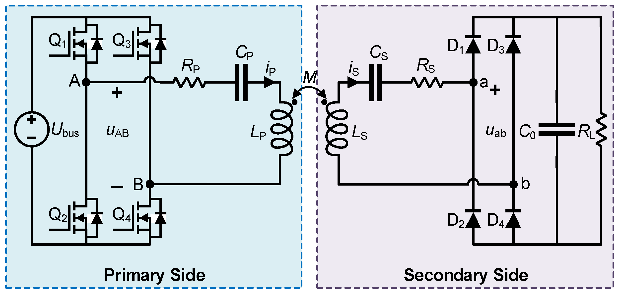
2. Modeling of SS-Compensated Wireless Charging System

Figure 1 shows the schematic diagram of the wireless charging system with SS compensation. Where U b u s is the DC bus voltage on the transmitter side; u A B is the AC voltage after the high-frequency inverter; u a b is the AC voltage before the rectifier bridge on the receiver side; i P is the current on the transmitter side; i S is the current on the receiver side; R P is the equivalent series resistance of the transmitter; R S is the equivalent series resistance of the receiver; R L is the load resistance; Q1–Q4 are the four MOSFETs of the inverter on the transmitter side; D1–D4 are the four diodes of the rectifier bridge on the receiver side; L P and L S are the self-inductances of the transmitting and receiving coils, respectively; C P and C S are the compensation capacitors on the transmitter and receiver sides, respectively; M is the mutual inductance between the transmitting and receiving coils; and C 0 is the filter capacitor.
Both u A B and u a b are square-wave voltages at angular frequency ω , whose Fourier series expansions are given in Equation (1). Neglecting higher-order harmonics, the SS-compensated wireless charging system can be represented by the simplified equivalent circuit shown in Figure 2, where the fundamental voltage component u A B _ 1 s t and the equivalent load resistance R eq are determined by Equations (2) and (3), respectively.
u A B = 4 U b u s π s i n ω t + 1 3 s i n 3 ω t + 1 5 s i n 5 ω t + + 1 n s i n n ω t +
u A B 1 s t t = 4 U bus π s i n ω t
R eq = 8 π 2 R L
This system is mathematically described by the following phasor-domain equation set:
U A B 1 s t = R P + j X P I P j ω M I S j ω M I P = j X S + R S + R L I S              
where U A B _ 1 s t , I P , and I S are the phasor representations of the input voltage fundamental component, transmitter current, and receiver current, respectively; X P and X S denote the reactances of the compensation networks on the transmitter and receiver sides, respectively, where X P = ω L P 1 / ω C P and X S = ω L S 1 / ω C S .
Figure 2 can be further simplified into a mutual inductance model of the wireless charging system, as illustrated in Figure 3. According to the circuit theory analysis, the expressions for key parameters of the SS-compensated wireless charging system can be derived, including input impedance, input impedance angle, input voltage/current, and output voltage/current.
The input impedance Z i n of the SS-compensated wireless charging system is given by
Z i n = R P + ω M 2 R S + R e q R S + R e q 2 + X S 2 + j X P ω M 2 X S R S + R e q 2 + X S 2
The magnitude of the input impedance | Z i n | is expressed in Equation (6).
| Z i n | = R S + R e q 2 R S + R e q 2 + X S 2 R P + ω M 2 R S + R e q X P X S R S + R e q 2 + X P + R P R S + R eq X S 2
The phase angle θ of the input impedance is given by
tan θ = I m Z in R e Z in = 1 R e Z in X P 1 R S + R e q 1 R P R e Z in X S
where R e Z in is the real part and I m Z in the imaginary part of the input impedance Z in , respectively. Furthermore, the expressions for output power and transmission efficiency are given as follows:
P out = ω M U AB _ 1 st 2 R eq ω M 2 + R S + R eq R P X P X S 2 + R S + R eq X P + R P X S 2
η = P out P in = 1 1 + R S R eq + R P R eq R eq + R S 2 ω M 2 + R P R eq X S 2 ω M 2
Particularly, numerous studies neglect system mistuning and equivalent internal resistance, focusing solely on the characteristics of the SS-compensated wireless charging system operating at the resonant angular frequency ω 0 , as shown in Equation (10).
Z i n = ω 0 M 2 R e q tan θ = 0 P out = U AB _ 1 st ω 0 M 2 R eq η = 1 1 + R S R eq + R P R eq R eq + R S 2 ω 0 M 2

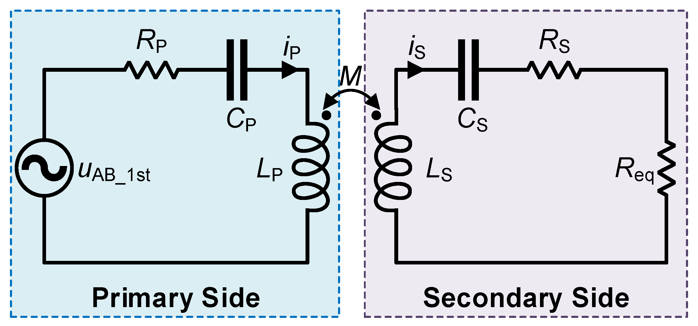
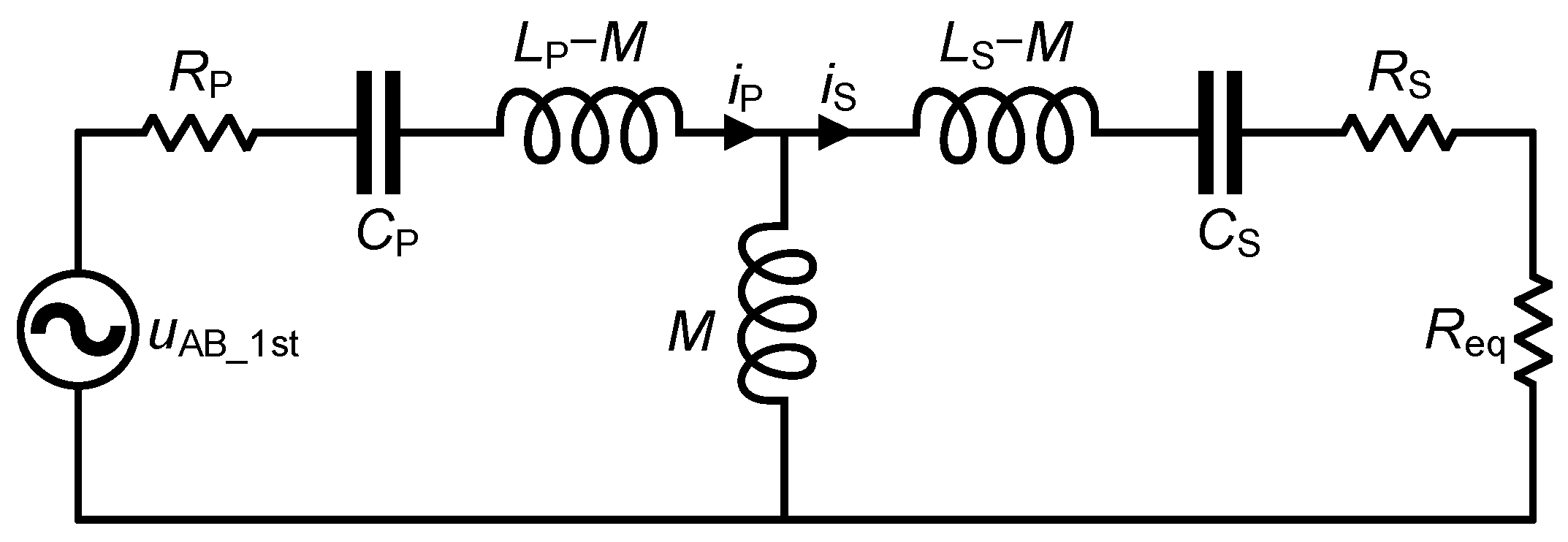
3. Modeling and Analysis of Mistuned SS-Compensated Wireless Charging Systems

While the conventional SS-compensated wireless charging system model demonstrates broad applicability, it lacks clarity in representing mistuning effects. This study develops a deviation-ratio-based methodology for analyzing mistuned SS-compensated wireless charging systems.

3.1. Equivalent Transformation of Mistuned System Parameters

Let L P 0 denote the nominal value of the transmitter coil self-inductance, L S 0 denote the nominal value of the receiver coil self-inductance, C P 0 denote the nominal value of the transmitter compensation capacitance, C S 0 denote the nominal value of the receiver compensation capacitance, and ω 0 denote the nominal resonant angular frequency, respectively. The resonance condition yields
X P 0 = ω 0 L P 0 1 ω 0 C P 0 = 0 , X S 0 = ω 0 L S 0 1 ω 0 C S 0 = 0
where X P 0 denotes the reactance of the transmitting side compensation network at resonance and X S 0 represents the reactance of the receiving side compensation network at resonance. Based on the resonant condition, the following key parameters of the system are defined as follows:
Q L 0 = ω 0 L S 0 / R eq Q P 0 = ω 0 L P 0 / R P Q S 0 = ω 0 L S 0 / R S k = M / L P 0 L S 0 f n = f / f 0 = ω / ω 0
where Q L 0 is the nominal loaded quality factor, Q P 0 is the transmitting side nominal quality factor, Q S 0 is the receiving side nominal quality factor, k is the nominal coupling coefficient, and f n is the normalized frequency.
Both manufacturing tolerances in coils/capacitors and operational parameter drifting in inductances/capacitances can induce mistuning in wireless charging systems. This causes the system to deviate from its optimal operating point and may even result in the loss of zero-voltage switching (ZVS). To quantitatively characterize the mistuning effects caused by parameter deviations in SS-compensated wireless charging systems, we define the following normalized deviation parameters as follows:
δ L P = L P / L P 0 δ L S = L S / L S 0 δ C P = C P / C P 0 δ C S = C S / C S 0 ,
where δ L P and δ L S represent the deviation ratios of the self-inductance of the coils on the transmitting and receiving sides, respectively; δ C P and δ C S denote the deviation ratios of compensation capacitances on the transmitting and receiving sides, respectively.
The relationship between capacitance and inductance deviation ratios can be mathematically transformed according to Equation (14).
δ L P = 1 f n 2 δ C P 1 + δ C P δ L S = 1 f n 2 δ C S 1 + δ C S
The reactances of the compensation networks on the transmitting and receiving sides of the mistuned SS-compensated wireless charging system can be expressed as follows:
X P = f n ω 0 L P 0 χ L P X S = f n ω 0 L S 0 χ L S
where
χ L P = 1 + δ L P 1 f n 2 χ L S = 1 + δ L S 1 f n 2

3.2. Analysis of Input Impedance of Mistuned SS-Compensated Wireless Charging Systems

3.2.1. Input Impedance Characterization

According to the analysis presented in Section 2, the input impedance characteristics of the SS-compensated wireless charging system are determined by Equation (5). By combining Equations (5), (16) and (17), the relationship between the input impedance and deviations in system component parameters can be established. Since the deviation ratio of compensation capacitors can be equivalently converted to that of self-inductances, this study exclusively focuses on the self-inductance deviations. Under these conditions, the real component of the input impedance, R e Z in , can be expressed as follows:
R e Z in = ω 0 L P 0 1 Q P 0 + k 2 f n 2 1 Q S 0 + 1 Q L 0 1 Q S 0 + 1 Q L 0 2 + f n 2 χ L S 2
The imaginary component, I m Z in , can be expressed as
I m Z in = f n ω 0 L P 0 χ L P k 2 f n 2 χ L S 1 Q S 0 + 1 Q L 0 2 + f n 2 χ L S 2
The amplitude of the input impedance, Z i n , is given by Z i n = R e Z in 2 + I m Z in 2 .
As for the input impedance angle, when the equivalent series resistance is taken into account, the tangent of the input impedance angle can be expressed as
tan θ = 1 Q S 0 + 1 Q L 0 2 + f n 2 χ L S 2 f n χ L P f n 3 k 2 χ L S 1 Q S 0 + 1 Q L 0 2 + f n 2 χ L S 2 1 Q P 0 + f n 2 k 2 1 Q S 0 + 1 Q L 0
The above analysis demonstrates that the system input impedance (both its magnitude and phase angle) exhibits a nonlinear dependence on parameter deviations ( δ L P and δ L S ). Moreover, this dependence is also affected by the operating frequency, equivalent series resistance, and load resistance.

3.2.2. Condition of Neglecting the Equivalent Series Resistance

When the load resistance is disregarded, the system should meet the following requirements:
( δ L P , δ L S , R e q , k , f n ) Γ , Γ = ( δ L P , δ L S , R e q , k , f n ) Φ Φ R 0 Φ R 0 < ε
where Φ is the characteristic function set of the mistuned SS-compensated wireless charging system, including Z i n , tan θ , I P , I S , and P out ; Φ R 0 is the characteristic function set without considering series resistance; and ε is the relative error ratio.
Specifically, as commonly adopted in previous studies, when analyzing the resonant SS-compensated wireless charging system exclusively, both the reactance of the compensation network on the transmitter side ( X P ) and the reactance of the compensation network on the receiver side ( X S ) in Equation (5) equal zero. Consequently, the imaginary part of the system impedance Z i n is zero, exhibiting purely resistive characteristics that we denote as Z i n X 0 .
Z i n X 0 Z i n | X P , X S = 0 = R P + ω 0 M 2 R S + R e q
According to (23), when the load resistance is large or the coil coupling is weak, the equivalent series resistance on the transmitter side cannot be neglected; when the load resistance is relatively small, the equivalent series resistance on the receiver side is not negligible. From the perspective of system impedance analysis, if
R P     ϵ ω 0 M 2 R S + R eq R S     ϵ R eq
then the equivalent series resistance of the receiver side and transmitter side can be neglected. Where ϵ is the proportionality coefficient, selected according to the actual situation. Accordingly, the equivalent load resistance R eq of the SS-compensated wireless charging system at resonance must satisfy the following conditions to ensure negligible equivalent series resistance:
R S ϵ R e q ϵ ω 0 M 2 R P R S
In Equation (23), the lower limit of the equivalent load, R S / ϵ , is determined by the equivalent series resistance on the receiver side, while the upper limit, ϵ ω 0 M 2 / R P R S , depends on the resonant frequency, the equivalent resistances of the receiver and transmitter sides, and the coupling between the receiving and transmitting coils. In a wireless charging system, the equivalent load resistance reaches its minimum value at the initial stage of constant-current charging and gradually increases during the charging process. Given the parameters where ϵ = 0.01 , R P = R S = 0.1   Ω , f 0 = 85   k H z and M = 45   μ H , the equivalent load resistance varies within the range of 10 Ω to 57.7 Ω . As evident, the range of equivalent load resistance defined by Equation (25) is relatively limited, necessitating careful consideration in the design process.
From Equation (23), it can be observed that if the equivalent series resistance of the SS-compensated wireless charging system is neglected, the coupling coefficient must satisfy the following conditions during system operation:
k R P R S + R e q ϵ ω 0 2 L P 0 L S 0 = 1 ϵ 1 Q P 0 1 Q S 0 + 1 Q L 0
Therefore, for the SS-compensated wireless charging system, the equivalent resistances at both the receiver and transmitter sides cannot be neglected under weak coupling conditions.

3.2.3. Input Impedance Characteristics Analysis Under Neglected Equivalent Series Resistance

When the equivalent series resistances at the transmitter and receiver sides are neglected, the system input impedance Z i n can be expressed as
Z i n R 0 Z i n | R P , R S = 0 = ω M 2 R e q R e q 2 + X S 2 + j X P ω M 2 X S R e q 2 + X S 2
The tangent of the input impedance angle θ of the system is given by
tan θ | R P , R S = 0 = X P R e Z inR 0 X S R e q
As indicated by Equation (26), when the series resistance is neglected, the input impedance angle is determined by the difference between the ratio of the transmitter-side compensation network reactance to the input resistance and the ratio of the receiver-side compensation network reactance to the equivalent load resistance. This difference governs the impedance characteristics of the system. If the difference is positive, the system exhibits inductive behavior; if the difference is negative, the system exhibits capacitive behavior. Specifically, when X P is positive and X S is non-positive, the input impedance angle is positive, and the entire wireless charging system presents an inductive characteristic. On the other hand, when X P is negative and X S is non-negative, the input impedance angle is negative, and the entire wireless charging system behaves capacitively. Furthermore, if only the mistuned reactance from either the transmitter or receiver side is considered, the input impedance angle is directly proportional to the reactance of the transmitter-side compensation network but inversely proportional to the reactance of the receiver-side compensation network.
When the equivalent series resistances are neglected and the system operates at the nominal resonant frequency (i.e., R P = 0 ,   R S = 0 ,   f n = 1 ), the tangent of the input impedance angle is given by
tan θ = Q L 0 1 k 2 δ L P δ L S 2 + 1 k 2 Q L 0 2 δ L P δ L S δ L P , δ L S 0 1 k 2 Q L 0 δ L P , δ L S = 0 Q L 0 δ L S , δ L P = 0
As can be seen from Equation (27), the input impedance angle at the nominal resonant frequency is influenced by the loaded quality factor, coupling coefficient, parameter deviation ratio on the transmitter side, and parameter deviation ratio on the receiver side, exhibiting relatively complex nonlinearity. The tangent of the input impedance angle consists of three components:
  • A four-parameter coupling term involving the loaded quality factor, the deviation ratio of the transmitter coil self-inductance, the deviation ratio of the receiver coil self-inductance, and the coupling coefficient;
  • A three-parameter coupling term involving the loaded quality factor, the deviation ratio of the transmitter coil self-inductance, and the coupling coefficient;
  • A two-parameter coupling involving the loaded quality factor and the deviation ratio of the receiver coil self-inductance.
For systems considering only receiver-side parameter deviations, the input impedance angle is affected by the load and receiver coil self-inductance deviation ratios. For systems considering only transmitter-side parameter deviations, the input impedance angle is influenced not only by the load and receiver coil self-inductance deviation ratios but also by the coupling coefficient. Given that the deviation ratios of self-inductance and capacitance can be equivalently interchanged, the following conclusions can be drawn:
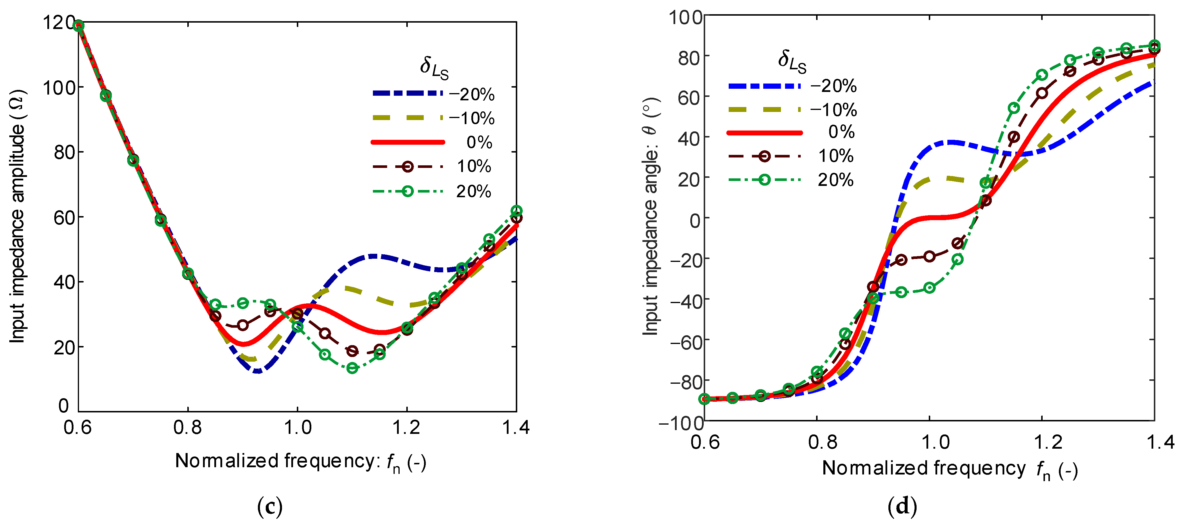
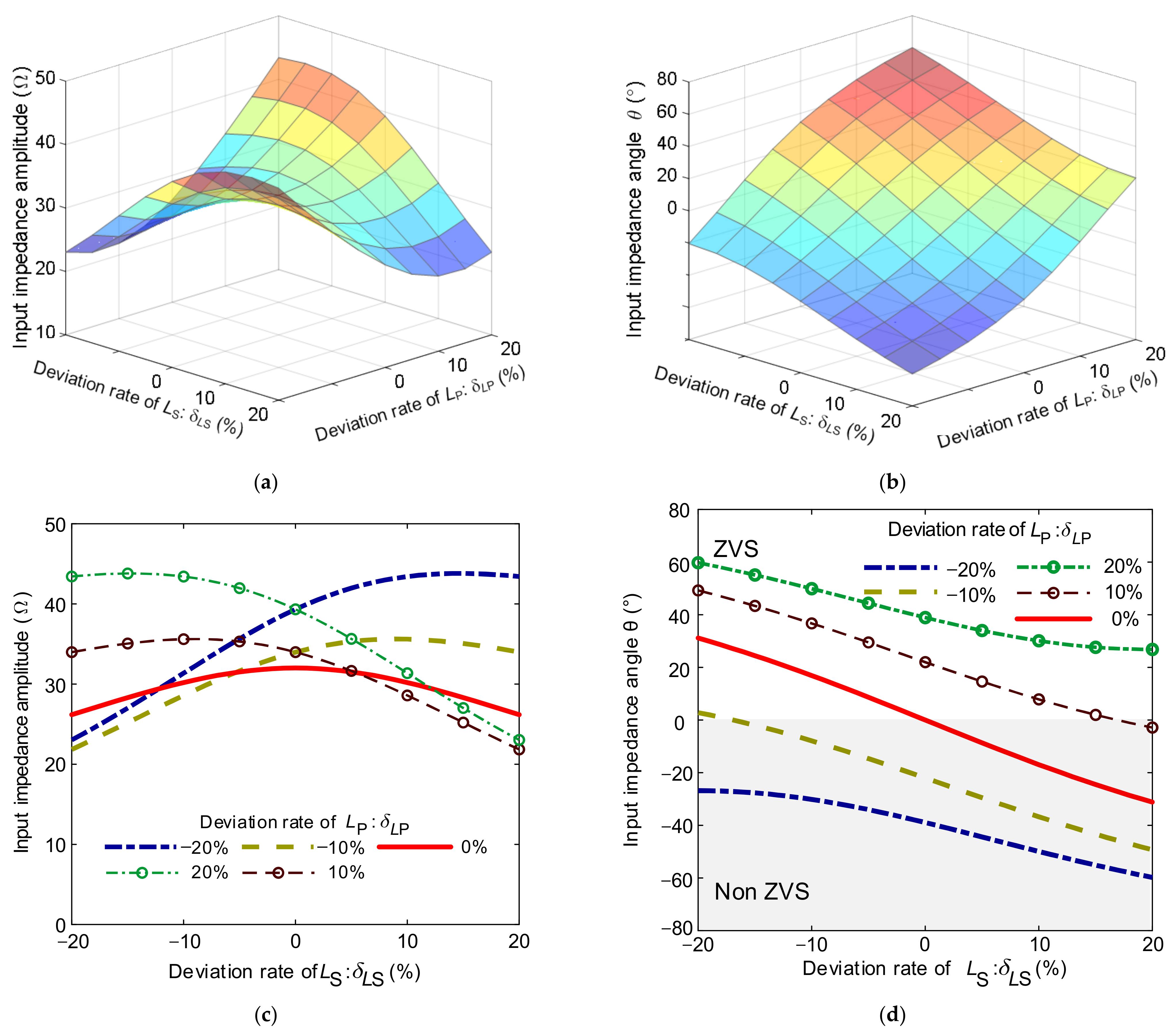
  • Decreasing the receiver-side self-inductance or its compensation capacitance will result in a positive input impedance angle, causing the entire SS-compensated wireless charging system to exhibit inductive characteristics.
  • Increasing the transmitter-side self-inductance or its compensation capacitance will also result in a positive input impedance angle, making the SS-compensated system behave inductively.
Therefore, to ensure zero-voltage switching (ZVS) of the MOSFETs in the high-frequency inverter of an SS-compensated wireless charging system, the design should either make the transmitter-side self-inductance or its compensation capacitance slightly larger than its resonant value or make the receiver-side self-inductance or its compensation capacitance slightly smaller than its resonant value.

3.3. Efficiency of Mistuned SS-Compensated Wireless Charging System

When considering parameter deviations, the efficiency of the SS-compensated wireless charging system can be expressed as follows:
η = 1 1 + Q L 0 Q S 0 + Q L 0 k 2 Q P 0 1 f n 2 Q L 0 2 1 + Q L 0 Q S 0 2 + 1 + δ L S 1 f n 2 2
As can be seen from Equations (11) and (30), the transmission efficiency η of the SS-compensated wireless charging system exhibits dependence on multiple parameters including the nominal quality factors of both the transmitter and receiver sides, the nominal loaded quality factor of the system, the coupling coefficient, the operating frequency, etc. Notably, the efficiency exhibits unique sensitivity characteristics—being susceptible to parameter deviations of the receiver side while remarkably maintaining insensitivity to the parameter variations in the transmitter side.
Let
η Q L 0 = 0
the efficiency-optimized nominal loaded quality factor can be expressed as
Q L 0 _ opt = 1 Q P 0 Q S 0 f n 2 k 2 + 1 Q S 0 2 + f n 2 1 + δ L S 1 f n 2 2
Consequently, the load equivalent resistance with optimum efficiency can be obtained by
R e q _ o p t = ω 0 L S 0 Q P 0 Q S 0 f n 2 k 2 + 1 Q S 0 2 + f n 2 1 + δ L S 1 f n 2 2
Thus, the efficiency of the SS-compensated wireless charging system is obtained by
η R eq _ opt = 1 1 + 2 k 2 f n 2 Q P 0 1 Q S 0 + R e q _ o p t ω 0 L S 0
Let
η f n = 0
the efficiency-optimized normalized frequency can be expressed as
f n _ o p t = 1 1 + δ L S 1 2 Q L 0 2 1 + Q L 0 Q S 0 2
Under this condition, the efficiency of the SS-compensated wireless charging system can be expressed as follows:
η f n _ o p t = 1 1 + Q L 0 Q S 0 + 1 k 2 Q L 0 Q P 0 f n _ opt 2 1 + Q L 0 Q S 0 2 + 1 4 k 2 Q L 0 3 Q P 0 1 + Q L 0 Q S 0 4
Let
η δ L S = 0
The efficiency-optimized parameter deviation of the receiver side is obtained as follows:
δ L S _ opt = 1 f n 2 1
It is evident that the receiver side is in resonance under these conditions, and
R L _ opt = ω 0 L S 0 Q S 0 1 + f n 2 k 2 Q P 0 Q S 0 = R S 1 + f n 2 k 2 Q P 0 Q S 0
Thus, the efficiency of the SS-compensated wireless charging system under the efficiency-optimized parameter deviation of the receiver side is
η δ L S _ opt = 1 1 + Q L 0 Q S 0 + 1 k 2 f n 2 Q L 0 Q P 0 1 + Q L 0 Q S 0 2

3.4. Output Power of Mistuned SS-Compensated Wireless Charging System

From the previous analysis, Equation (10) can be rewritten as follows:
P out = G P P 0
where P 0 represents the output power of the ideal system operating at the nominal resonant frequency without considering the series equivalent internal resistance and parameter variations, which can be expressed as follows:
P 0 = U AB _ 1 st ω M 2 R eq = U AB _ 1 st 2 k 2 Q L 0 ω 0 L P 0
where G P denotes the power gain of the mistuned wireless charging system, defined as the ratio of the output power P out to the output power P 0 of the ideal system operating at the resonant frequency without considering the series equivalent internal resistance and parameter variations. The expression is given by
G P = 1 f n 2 1 + 1 k 2 1 f n 1 Q L 0 + 1 Q S 0 1 Q P 0 1 k 2 χ L P χ L S 2 + 1 k 4 1 Q L 0 + 1 Q S 0 χ L P + 1 Q P 0 χ L S 2
If the series equivalent resistance of the system is neglected and the parameter deviation ratios are introduced, the power gain of the mistuned wireless charging system can be further rewritten as
G P = 1 f n 2 1 1 k 2 χ L P χ L S 2 + 1 k 4 Q L 0 2 χ L P 2
In particular, when the system operates at the nominal resonant frequency f 0 , (i.e., f n = 1 ), the following equation can be obtained:
G P = 1 1 2 k 2 δ L P δ L S + 1 k 4 δ L P 2 δ L S 2 + 1 k 4 Q L 0 2 δ L P 2 , R P , R S = 0 , f n = 1 k 4 Q L 0 2 k 4 Q L 0 2 + δ L P 2 , R P , R S , δ L S = 0 , f n = 1     1 , R P , R S , δ L P = 0 , f n = 1
From Equation (44), it can be observed that the denominator of the power gain consists of four terms:
  • The first term is a constant term 1;
  • The second and third terms are the coupling terms between the self-inductance deviation ratios of the transmitter and receiver coils ( δ L P , δ L S ) and the coupling coefficient ( k );
  • The fourth term is a coupling term involving the self-inductance deviation ratio of the transmitter coil ( δ L P ), the coupling coefficient ( k ), and the loaded quality factor ( Q L 0 ).
When the system operates at the nominal resonant frequency ( f 0 ) and there is no parameter variation on the transmitter side (i.e., δ L P = 0 , f n = 1 ), the power gain equals unity (i.e., G P = 1 ). Under these conditions, the resonant state and receiver-side parameter variations do not affect the power gain. Therefore, when further considering the analysis of the impedance characteristics of the mistuned SS-compensated wireless charging system presented earlier, it can be concluded that during the design phase, it is more appropriate to achieve ZVS by reducing the compensation capacitance on the receiver side rather than increasing the compensation capacitance on the transmitter side.

4. Simulation Analysis

To further analyze the characteristics of SS-compensated wireless charging systems while considering parameter deviations, a numerical simulation study is conducted. The parameters of the SS-compensated wireless charging system are listed in Table 2.

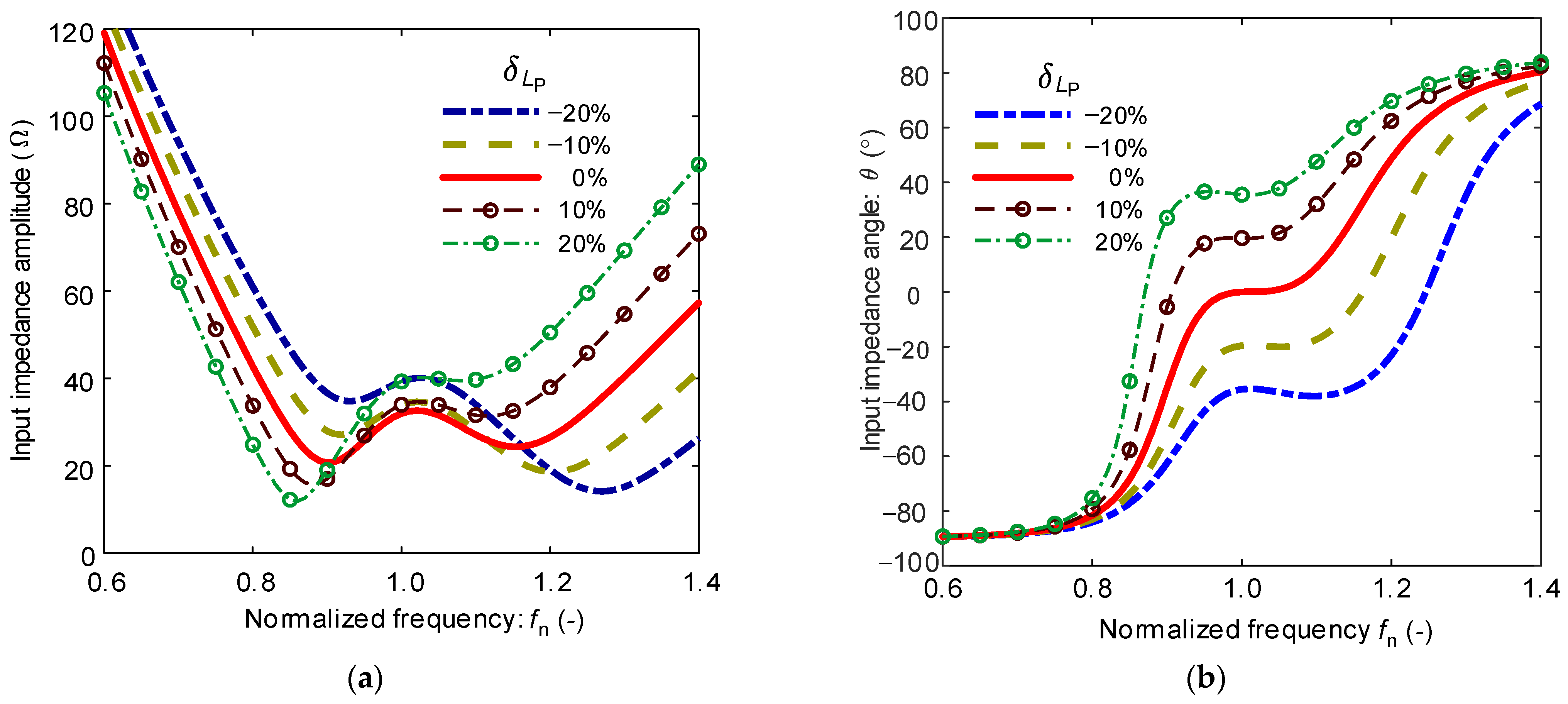
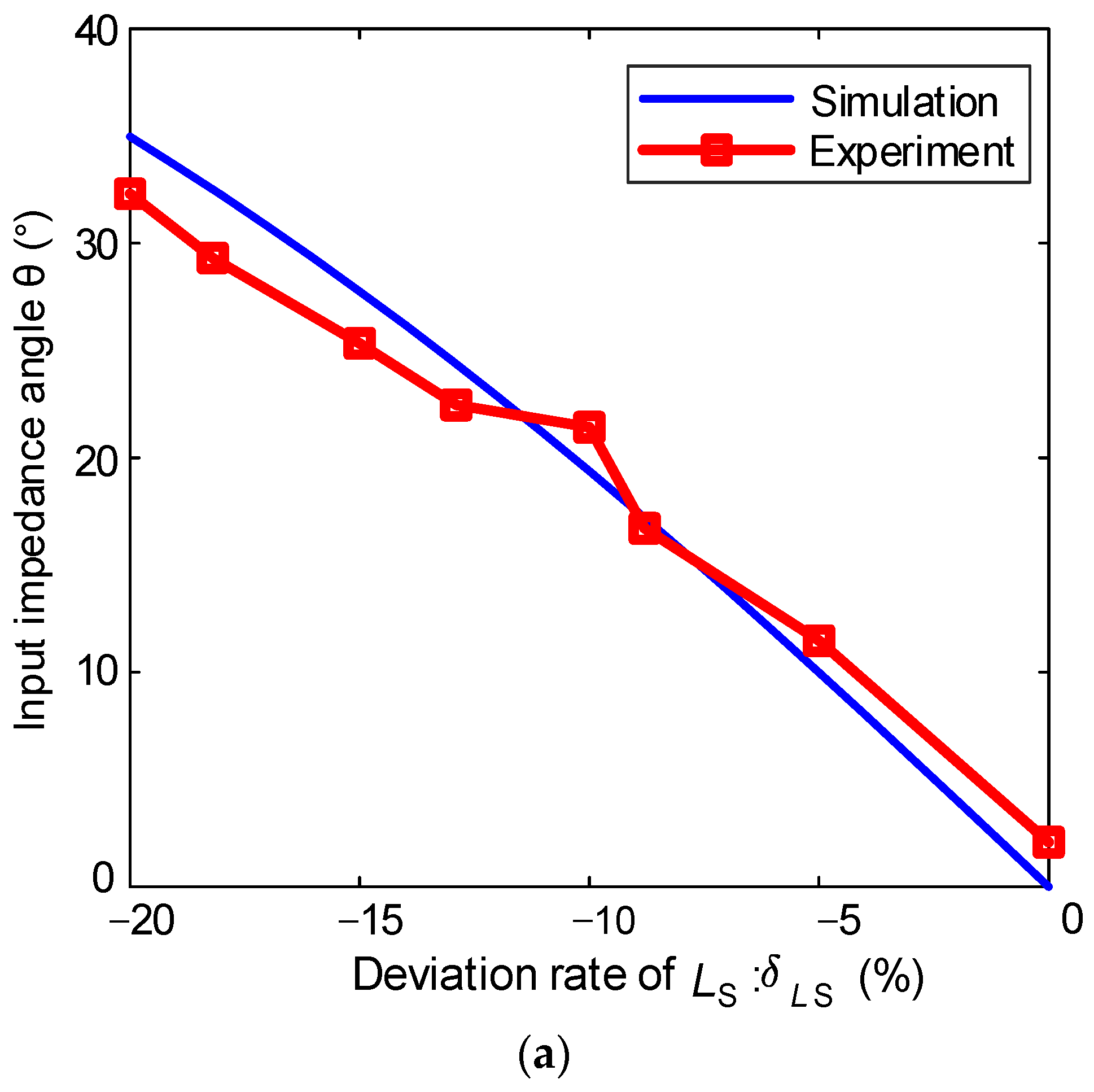
4.1. Simulation Analysis of Impedance Characteristics of Mistuned SS-Compensated Wireless Charging System

Figure 4 illustrates the frequency characteristics of the input impedance of the SS-compensated wireless charging system corresponding to different system parameters deviation ratios at the maximum coupling coefficient. Comparative analysis between Figure 4a,b and Figure 4c,d reveals that (1) the system undergoes frequency bifurcation phenomenon at high coupling coefficients; (2) transmitter side parameter deviations exert more significant influence on input impedance than receiver side deviations, with the latter only affecting impedance near the nominal resonant frequency ( f n ranging from 0.83 to 1.3). The analysis also reveals that (1) both positive and negative parameter deviations on the transmitter side increase the input impedance amplitude at the nominal resonant frequency ( f n = 1 ), while maintaining nearly constant peak amplitude with the same absolute deviations; (2) positive parameter deviations on the receiver side shift the peak to the left and the valley to the right, while negative deviations shift the peak to the right and the valley to the left; (3) positive parameter deviations on the transmitter side lead to an increase in the input impedance angle at the nominal resonant frequency ( f n = 1 ), while negative deviations result in a decrease in the input impedance angle; (4) positive parameter deviations on the receiver side lead to a decrease in the input impedance angle at the nominal resonant frequency ( f n = 1 ), while negative deviations result in an increase in the input impedance angle.
Figure 5a and Figure 5b, respectively, show the three-dimensional relationships of the input impedance magnitude and input impedance angle as functions of the transmitter coil self-inductance deviation ratio and receiver coil self-inductance deviation ratio for the SS-compensated wireless charging system operating at the nominal resonant frequency ( f n = 1 ) with maximum coupling (k = 0.28). Figure 5c and Figure 5d, respectively, illustrate the characteristics of the input impedance magnitude and input impedance angle as functions of the receiver coil self-inductance deviation ratio when the transmitter coil self-inductance deviation ratios are −20%, −10%, 0%, 10%, and 20%. As observed from Figure 5a,b, with zero transmitter-side parameter deviations (red thick solid line), the input impedance magnitude exhibits the smallest variation range with respect to receiving side inductance deviation; with positive transmitter-side parameter deviations, the input impedance magnitude shows positive correlation with receiver-side inductance deviation, accompanied by a rightward peak shift; with negative transmitter-side parameter deviations, the input impedance magnitude demonstrates negative correlation with receiver-side inductance deviation, accompanied by a leftward peak shift. From Figure 5c,d, it can be observed that the input impedance angle is positively correlated with the transmitter-side self-inductance deviation but negatively correlated with the receiver-side self-inductance deviation. When the transmitter-side parameters have no deviation, the input impedance angle varies approximately linearly with the receiver-side self-inductance deviation, which is consistent with the conclusion derived from Equation (27).
Figure 6 illustrates the variation characteristics of input impedance with respect to load resistance under different parameter deviation ratios. Figure 6a presents the variation curves of the input impedance magnitude versus load resistance under different transmitter-side self-inductance deviation ratios, showing an approximately inverse proportional relationship between the input impedance magnitude and load resistance. When the load resistance is small (less than 10 Ω), the transmitter parameter deviation ratio has negligible influence on the input impedance magnitude. However, at higher load resistances, the transmitter-side parameter deviation ratio significantly affects the input impedance magnitude, which exhibits a positive correlation with the absolute value of the deviation ratio. Figure 6b depicts the variation curves of the input impedance angle versus load resistance under different transmitter-side self-inductance deviation ratios. A positive transmitter-side parameter deviation results in a positive input impedance angle that increases with load resistance, whereas a negative deviation leads to a negative angle that decreases with load resistance. When the system’s series equivalent internal resistance is neglected, the input impedance angle shows an approximately linear relationship with load resistance. Figure 6c illustrates the variation curves of the input impedance magnitude versus load resistance under different receiver-side self-inductance deviation ratios, demonstrating that the input impedance magnitude decreases as the load resistance increases. For small load resistances, the receiver-side parameter deviation ratio has a considerable impact on the input impedance magnitude, which exhibits a negative correlation with the absolute value of the deviation ratio. However, when the load resistance exceeds 30 Ω, the receiver-side parameter deviation ratio has minimal effect on the input impedance magnitude. Figure 6d presents the variation curves of the input impedance angle versus load resistance under different receiver-side self-inductance deviation ratios. A positive receiver-side parameter deviation yields a negative input impedance angle that increases with load resistance, while a negative deviation produces a positive angle that decreases with load resistance. These observations are also consistent with the conclusions derived from Equation (29).

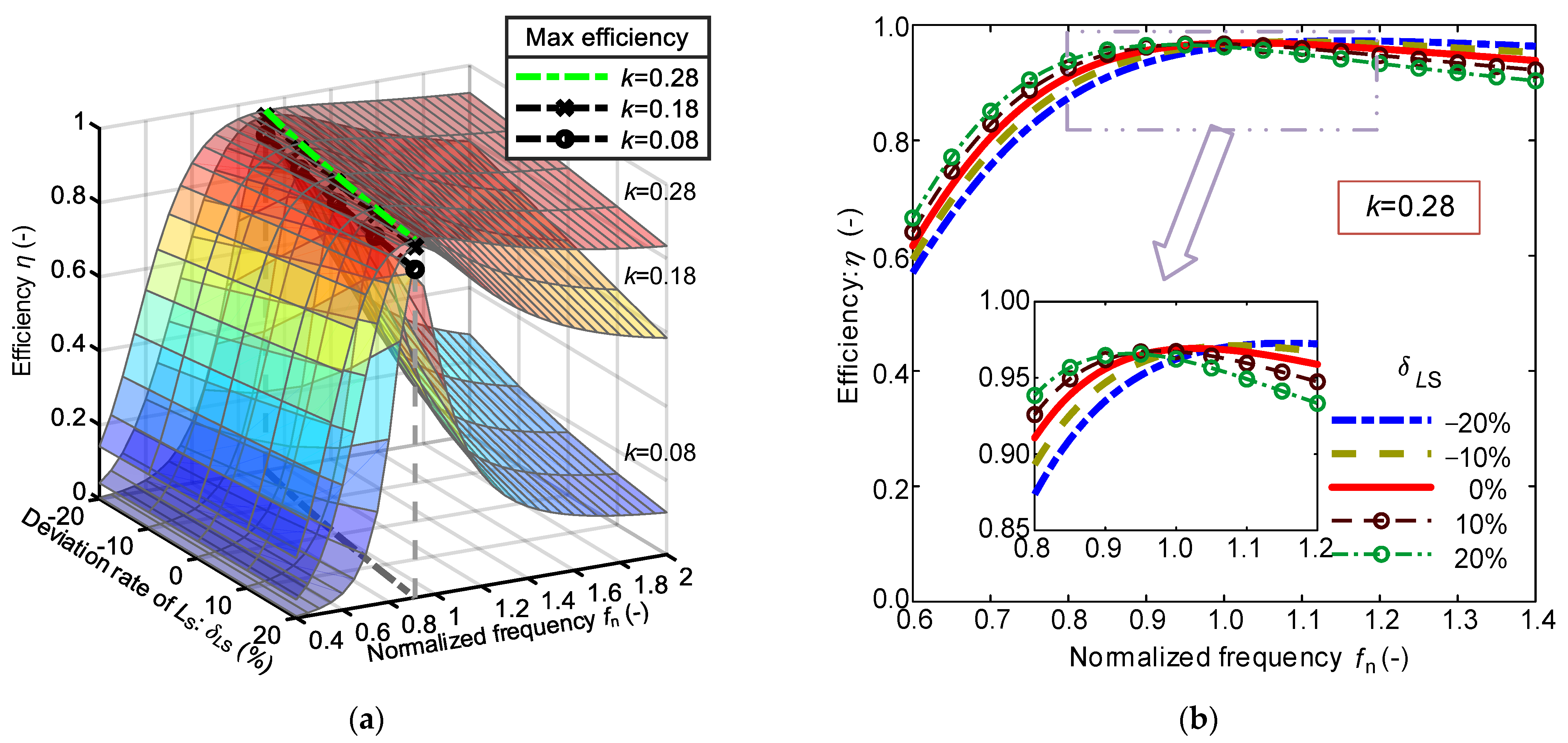
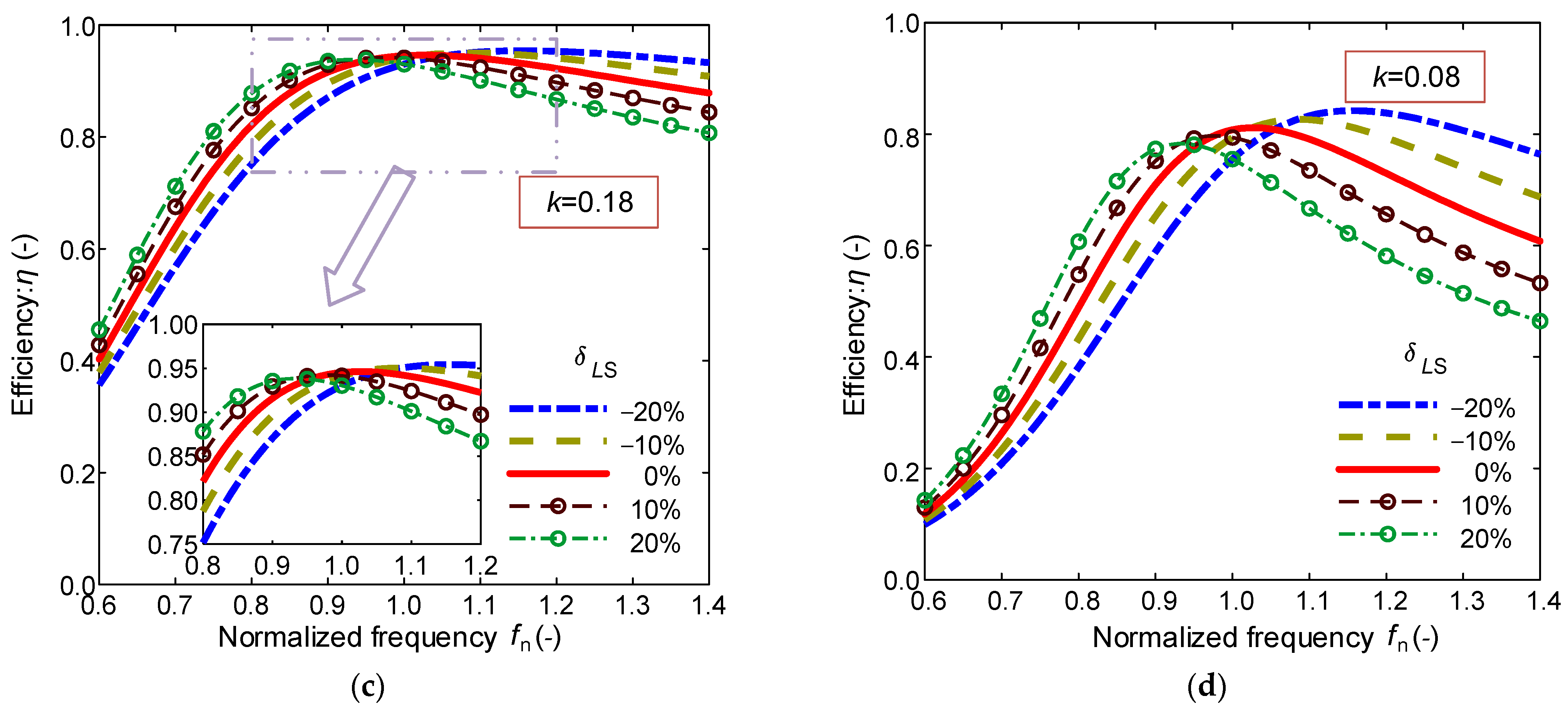
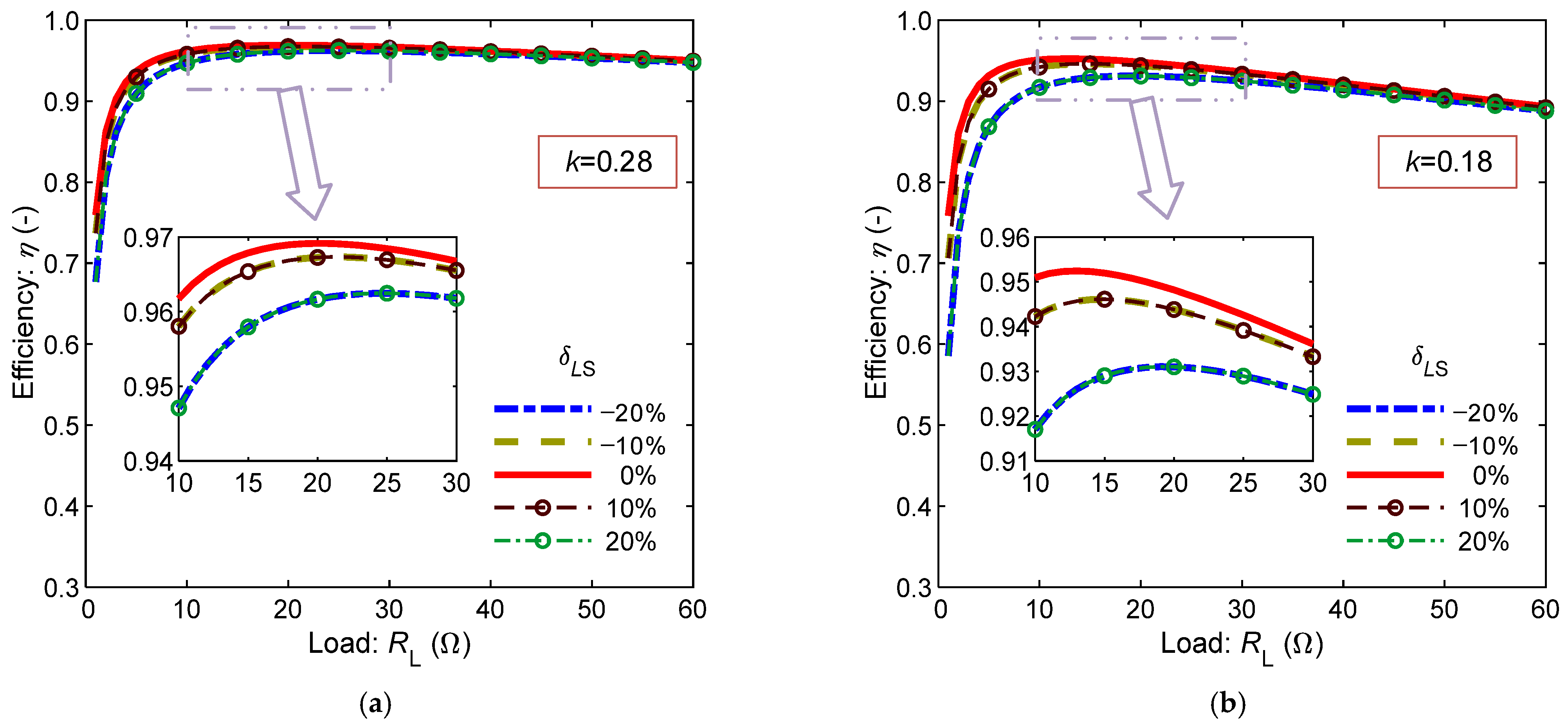
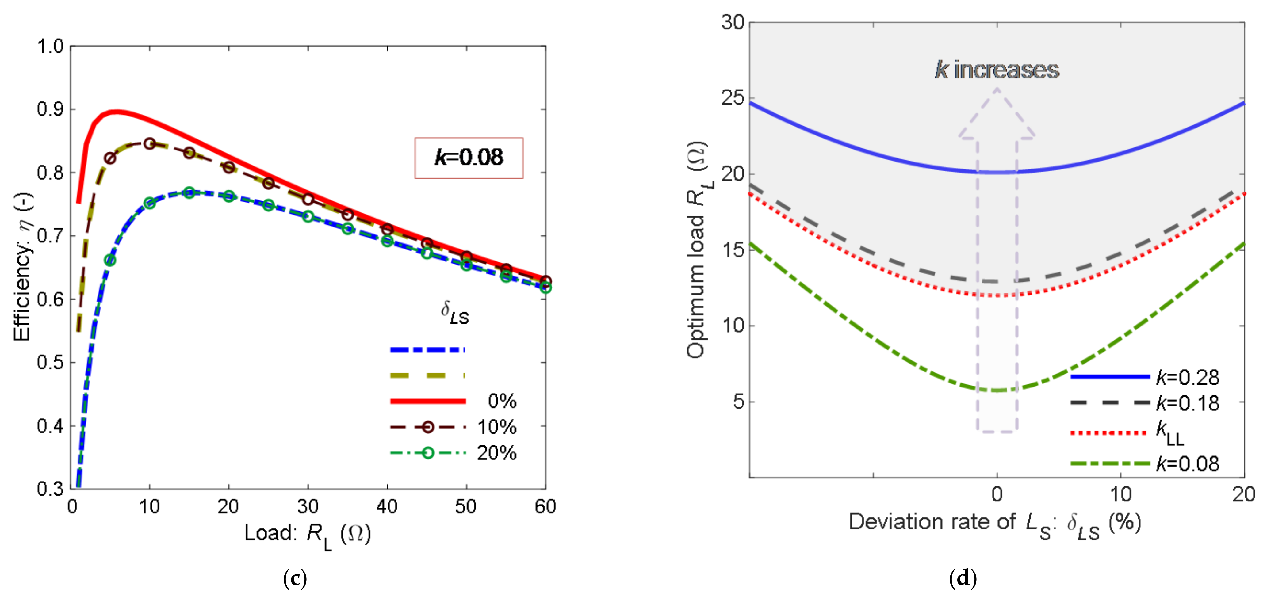
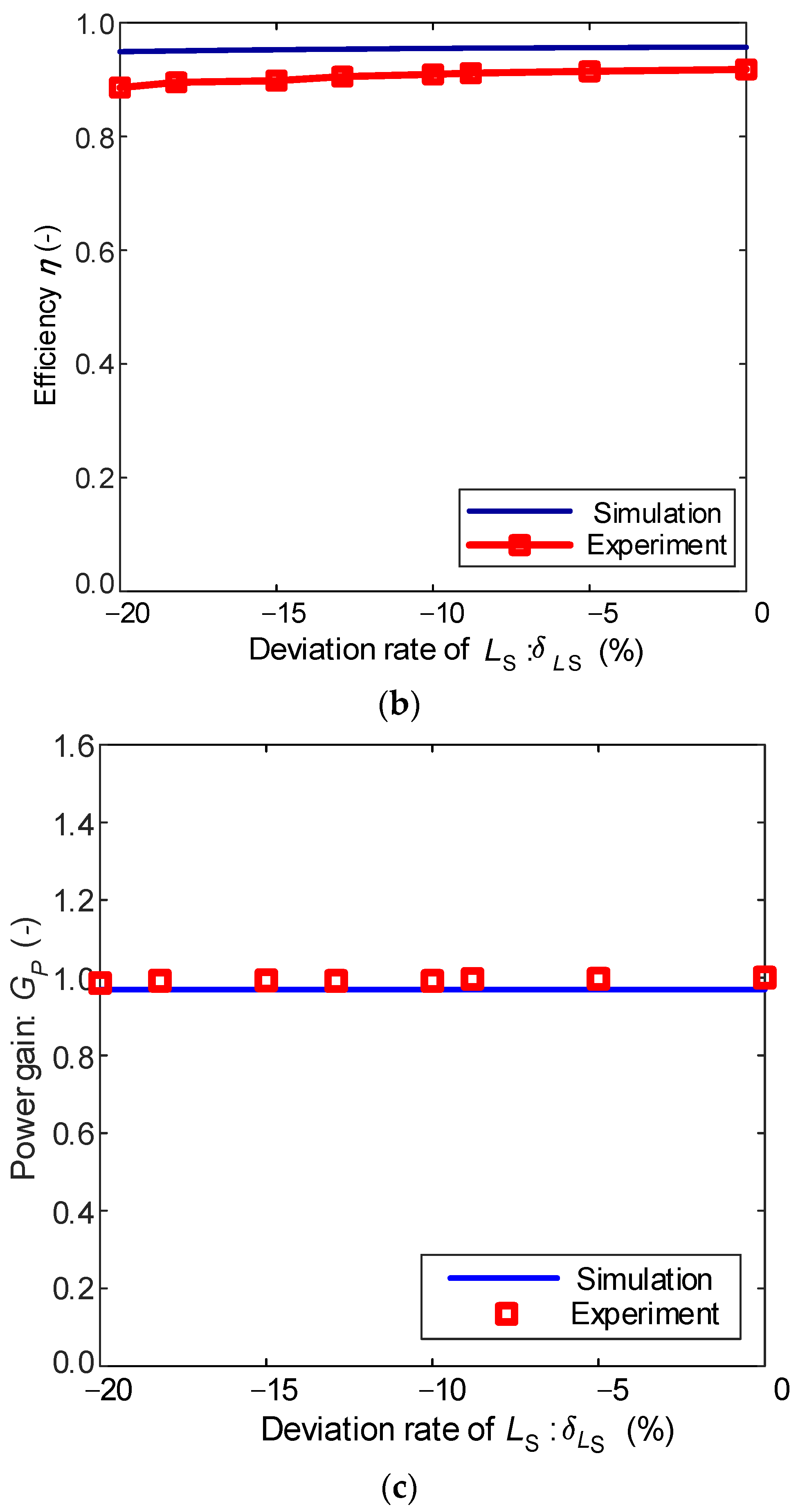
4.2. Simulation Analysis of Efficiency of Mistuned System

Figure 7 demonstrates the relationship between system efficiency versus frequency and receiver-side self-inductance deviation ratios under various coupling coefficients. The results reveal that (1) the operating point corresponding to the maximum efficiency (defined by both receiver-side self-inductance deviation ratio of and frequency) remains independent of the coupling coefficient; (2) the degree of influence of receiver-side self-inductance deviation on the efficiency exhibits a negative correlation with coupling coefficient, showing more significant influence under weaker coupling conditions; (3) positive receiver-side inductance deviation ratios induce a leftward shift in the peak efficiency point, while negative deviation ratios cause a rightward shift; (4) under the same coupling coefficient, negative receiver-side self-inductance deviation ratios increases the maximum efficiency of the system, whereas at the nominal resonance frequency, any self-inductance deviation degrades efficiency with the system efficiency being negatively correlated to the absolute value of the deviation ratio.
Figure 8 illustrates the system efficiency characteristics versus load resistance and receiver-side coil self-inductance deviation ratio under different coupling coefficients when operating at nominal resonant frequency. The results demonstrate that (1) system efficiency initially increases and subsequently decreases with increasing load resistance; (2) smaller coupling coefficients lead to both reduced maximum efficiency and enhanced sensitivity to load variations, while simultaneously amplifying the impact of receiver-side self-inductance deviation ratios; (3) under the same coupling coefficient, the maximum achievable efficiency shows a negative correlation with the absolute value of the self-inductance deviation ratio δ L S , with the optimal load resistance for peak efficiency increasing proportionally with δ L S . These findings systematically reveal the complex interdependence between coupling conditions, load matching, and parameter tolerances in SS-compensated wireless charging systems.
In summary, the following conclusions can be drawn: when the coupling coefficient is large, the influence of the receiving side parameter deviation ratios on the efficiency can be neglected, provided that the load resistance exceeds the optimal value; under low coupling conditions, the influence of the transmitter-side parameter deviation ratios on the efficiency becomes non-negligible, and the system should operate near the optimal load resistance to maintain performance.

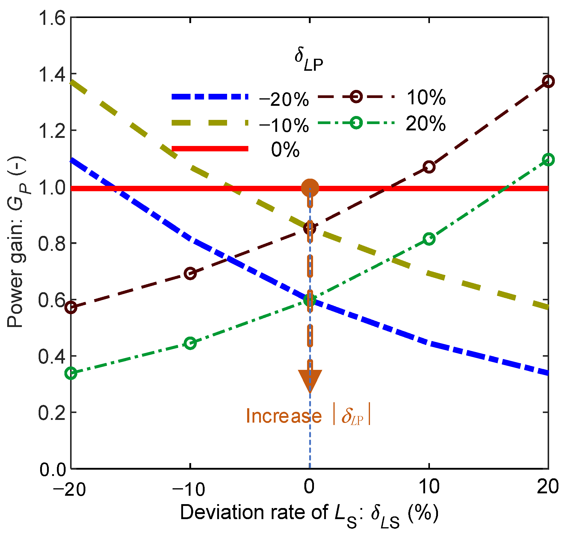
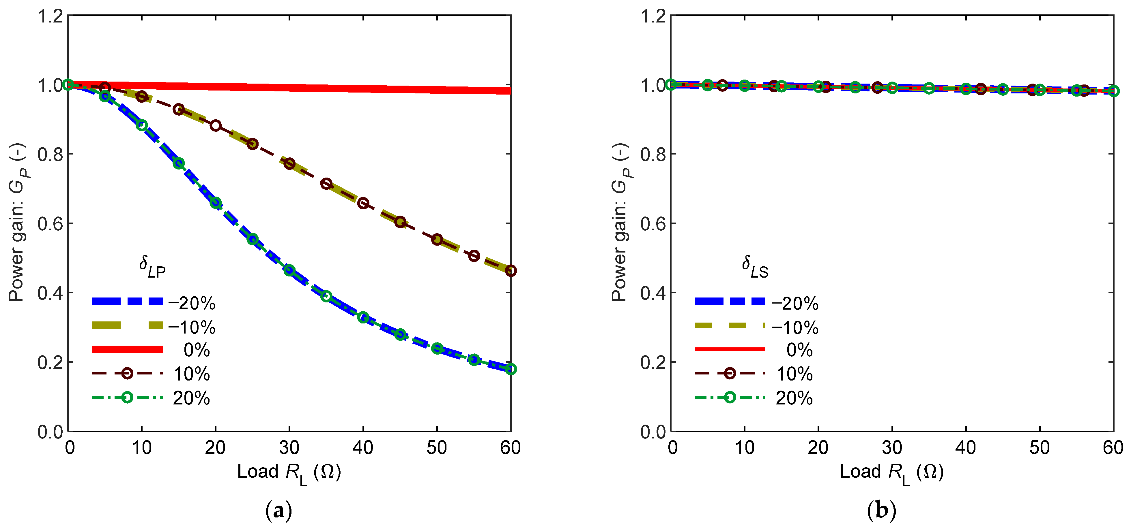
4.3. Simulation Analysis of Power Gain Characteristics of Mistuned Systems

Figure 9 presents the relationship between power gain and receiver-side self-inductance deviation ratio under different transmitter-side self-inductance deviation ratios when the system operates at the nominal resonant frequency. The results demonstrate three key observations: (1) when the transmitter-side parameters maintain nominal values (zero deviation), the receiver-side self-inductance deviations show negligible influence on power gain; (2) with zero receiver-side self-inductance deviation, the power gain decreases monotonically with increasing absolute values of transmitter-side self-inductance deviation; (3) under non-zero transmitter-side parameter deviations, the power gain exhibits opposite correlation patterns—negative transmitter-side parameter deviation ratios create negative correlation between power gain and receiver-side parameter deviation (with power gain reducing as negative deviation ratio increases), while positive transmitter-side parameter deviation ratios produce positive correlation (yet similarly showing reduced power gain with larger positive deviation ratios). These asymmetric characteristics reveal the complex cross-coupling effects between transmitter-side and receiver-side parameter deviation ratios in SS-compensated wireless charging systems.
Figure 10 presents the relationship curves between power gain and load resistance under different parameter deviation ratios when the system operates at the nominal resonant frequency. As shown in Figure 10a, when the system exhibits no parameter deviations, the power gain remains approximately unity without variation as load resistance increases. However, when deviations exist in the transmitter-side self-inductance, the power gain gradually decreases with increasing load resistance. Moreover, the larger the absolute value of the self-inductance deviation ratio, the faster the power gain decreases with increasing load resistance. From Figure 10b, it can be observed that if no parameter deviations occur on the transmitter side, the self-inductance deviation ratio on the receiver side has negligible influence on the power gain. The power gain remains consistently close to unity as the load resistance increases, which aligns with the conclusion derived from Equation (44).

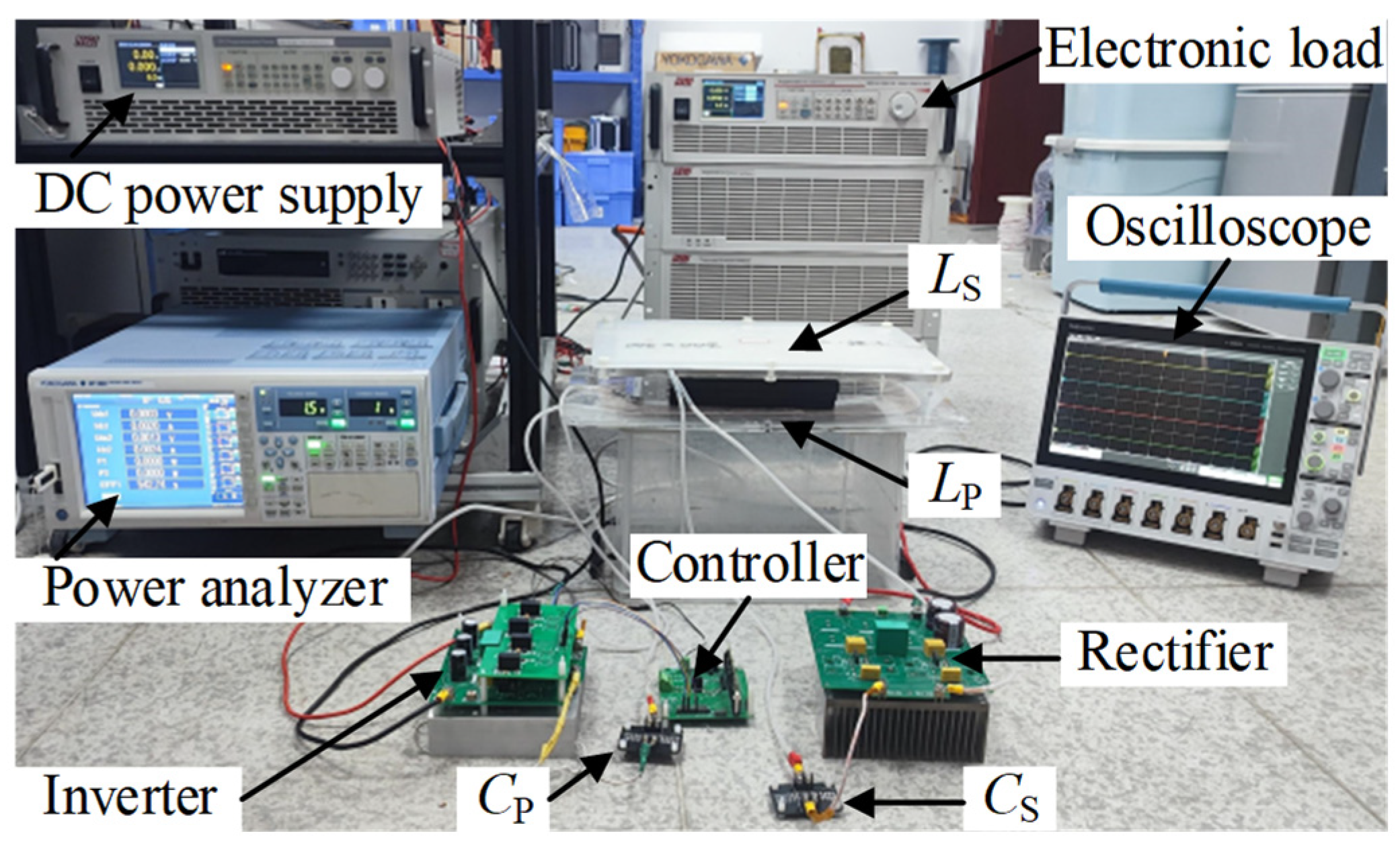
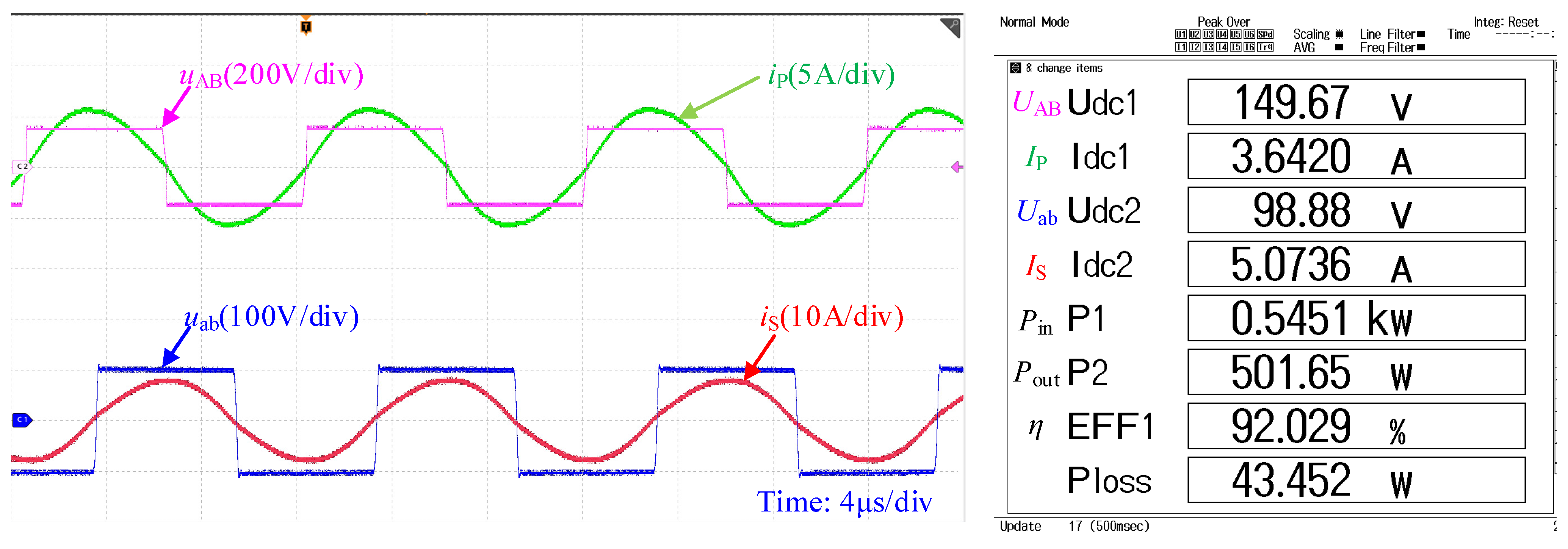
5. Experimental Verification

An experimental platform for a mistuned SS-compensated wireless charging system was conducted to validate the proposed mistuned SS-compensated wireless charging system model and its theoretical analysis. Both the transmitter and receiver coils employ a rectangular structure, wound with 100-strand 0.01 mm Litz wire. The transmitter coil consists of 13 turns with an outer dimension of 200 × 400 mm, while the receiver coil consists of 11 turns with an outer dimension of 200 × 300 mm, maintaining a 50 mm air gap between them. The input power is supplied by a controllable ACC/DC converter module. The high-frequency inverter, operating at 85 kHz, utilizes Infineon IPW60R099C6 MOSFETs (Infineon, Munich, Germany), with its switching signals generated by a TMS320F28335 digital controller (Texas Instruments, Dallas, TX, USA). On the receiver side, the high-frequency AC power is rectified using IDW20C65D2 diodes (Infineon, Munich, Germany), filtered, and then delivered to an electronic load. The experimental setup is shown in Figure 11, while Figure 12 presents the measured waveforms under optimal load conditions with nominal parameters.
Since adjusting the compensation capacitance in a wireless charging system is more practical than modifying the coil self-inductance, this study achieves parameter deviation variations in the SS-compensated wireless charging system by altering the compensation capacitance on both the transmitter and receiver sides. The capacitance deviation ratios are then converted into equivalent self-inductance deviation ratios according to Equation (16). Four experimental cases were designed with the compensation capacitances listed in Table 3. The nominal values of the series compensation capacitances are 16.38 nF for the transmitter side, and 32.16 nF for the receiver side. All compensation capacitors employ class I C0G multilayer ceramic capacitors (MLCCs) to ensure high stability. Except for the data specified in Table 3, all component parameters remain identical to those in Table 2.
Figure 13 presents the experimental results of the input impedance angle, DC/DC efficiency, and power gain for the mistuned SS-compensated wireless charging system under different negative self-inductance deviation ratios at the receiver side. As shown in Figure 13, the experimental results are generally agree well with the simulation results of the proposed mistuned SS-compensated wireless charging system model. Figure 13a demonstrates that negative receiver-side parameter deviation ratios result in a positive input impedance angle, indicating that the system exhibits inductive behavior. Furthermore, the input impedance angle increases approximately linearly with the increasing absolute value of the negative deviation ratios. Figure 13b reveals that the system efficiency gradually decreases as the receiver-side parameter deviation increases. However, under conditions of high coupling coefficient, the efficiency reduction remains below 4%. Figure 13c indicates that the power gain maintains around unity throughout the experiments, suggesting that the receiver-side parameter deviations have negligible influence on power gain.
As shown in Figure 14, the experimental results of the input impedance angle, DC/DC efficiency, and power gain for the mistuned SS-compensated wireless charging system with −5% receiver-side equivalent self-inductance deviation are compared with both the simulation results from the proposed mistuned system model and the ideal fundamental harmonic analysis (FHA) results. Comparative results demonstrate excellent agreement between the proposed mistuned SS-compensated WPT system model and experimental measurements in terms of efficiency, input impedance angle, and power gain. The maximum efficiency deviation remains within 5%, primarily attributable to omitted MOSFET conduction/switching losses and measurement errors in the analytical approach.

6. Conclusions

This study establishes a mistuned SS-compensated wireless charging system model and systematically investigates the influence of parameters deviations (including self-inductance, capacitance, and load resistance) on system characteristics such as input impedance, efficiency, and power transfer capability. Through theoretical analysis, simulation, and experimental validation, the following conclusions are drawn:
  • System mistuning in SS-compensated wireless charging systems, caused by manufacturing tolerances and dynamic charging process variations, significantly affects system input impedance, efficiency, and power characteristics. The transmitter-side parameter deviation ratios exhibit a substantially greater impact on both input impedance and power gain compared to receiver-side deviation ratios. Notably, receiver-side parameter deviation ratios influence system impedance within a narrow frequency band and have minimal effect on power gain.
  • Under conditions of strong coupling (high k), the influence of the receiver-side parameter deviation ratios on the efficiency can be neglected when the load resistance exceeds the optimal value. Conversely, in weak coupling scenarios, transmitter-side parameter deviations become non-negligible for efficiency considerations, and the system should operate near the optimal load resistance.
  • For practical implementation of SS-compensated wireless charging system, stringent component tolerance requirements should be applied to transmitter-side elements (coil and compensation capacitor), while relatively relaxed specifications may be adopted for receiver-side components. These findings provide theoretical guidance for system design optimization.
  • Experimental results demonstrate that the proposed model maintains maximum deviations within 5% for efficiency, 3% for input impedance angle, and 2% for power gain compared to experimental measurements, while exhibiting strong trend agreement. These findings confirm consistency between theoretical and experimental analyses, validating the model’s feasibility and thereby furnishing reliable theoretical support for control strategy development.

Author Contributions

Conceptualization, W.L.; methodology, W.L. and Y.H.; software, Y.H. and C.L.; validation, Y.H. and C.L.; formal analysis, Y.H.; investigation, Y.H.; resources, W.L.; data curation, W.L. and Y.H.; writing—original draft preparation, W.L., Y.H. and C.L.; writing—review and editing, Y.H. and W.L.; visualization, W.L.; supervision, W.L.; project administration, W.L.; funding acquisition, W.L. All authors have read and agreed to the published version of the manuscript.

Funding

This work was supported by the National Natural Science Foundation of China (Grant No. 52207232).

Data Availability Statement

The original contributions presented in the study are included in the article, further inquiries can be directed to the corresponding author.

Conflicts of Interest

The authors declare no conflicts of interest.

References

  1. Liu, Z.; Li, T.; Li, S.; Mi, C.C. Advancements and challenges in wireless power transfer: A comprehensive review. Nexus 2024, 1, 100014. [Google Scholar] [CrossRef]
  2. Detka, K.; Górecki, K. Wireless Power Transfer—A Review. Energies 2022, 15, 7236. [Google Scholar] [CrossRef]
  3. Xia, C.; Liu, L.; Liu, Y.; Ma, Z. IPT system for tail-free household appliances in the smart home system. IET Power Electron. 2019, 12, 1002–1010. [Google Scholar] [CrossRef]
  4. Sedehi, R.; Budgett, D.; Jiang, J.; Ziyi, X.; Dai, X.; Hu, A.P.; McCormick, D. A Wireless Power Method for Deeply Implanted Biomedical Devices via Capacitively Coupled Conductive Power Transfer. IEEE Trans. Power Electron. 2021, 36, 1870–1882. [Google Scholar] [CrossRef]
  5. Matsumoto, H.; Kanazawa, H.; Uwai, H.; Ishiwaka, R.; Sato, Y. Segment Switching Method of Three-Phase Wireless Power Transmitter for AGV. IEEE Trans. Ind. Electron. 2024, 71, 6490–6500. [Google Scholar] [CrossRef]
  6. Pahlavan, S.; Shooshtari, M.; Jafarabadi Ashtiani, S. Star-Shaped Coils in the Transmitter Array for Receiver Rotation Tolerance in Free-Moving Wireless Power Transfer Applications. Energies 2022, 15, 8643. [Google Scholar] [CrossRef]
  7. Niu, S.; Zhao, Q.; Chen, H.; Yu, H.; Niu, S.; Jian, L. Underwater Wireless Charging System of Unmanned Surface Vehicles with High Power, Large Misalignment Tolerance and Light Weight: Analysis, Design and Optimization. Energies 2022, 15, 9529. [Google Scholar] [CrossRef]
  8. Amjad, M.; Farooq-i-Azam, M.; Ni, Q.; Dong, M.; Ansari, E.A. Wireless charging systems for electric vehicles. Renew. Sustain. Energy Rev. 2022, 167, 112730. [Google Scholar] [CrossRef]
  9. Nguyen, H.T.; Alsawalhi, J.Y.; Hosani, K.A.; Al-Sumaiti, A.S.; Jaafari, K.A.A.; Byon, Y.-J.; Moursi, M.S.E. Review Map of Comparative Designs for Wireless High-Power Transfer Systems in EV Applications: Maximum Efficiency, ZPA, and CC/CV Modes at Fixed Resonance Frequency Independent From Coupling Coefficient. IEEE Trans. Power Electron. 2022, 37, 4857–4876. [Google Scholar] [CrossRef]
  10. Bagchi, A.C.; Kamineni, A.; Zane, R.A.; Carlson, R. Review and Comparative Analysis of Topologies and Control Methods in Dynamic Wireless Charging of Electric Vehicles. IEEE J. Emerg. Sel. Top. Power Electron. 2021, 9, 4947–4962. [Google Scholar] [CrossRef]
  11. Triviño, A.; González-González, J.M.; Aguado, J.A. Wireless Power Transfer Technologies Applied to Electric Vehicles: A Review. Energies 2021, 14, 1547. [Google Scholar] [CrossRef]
  12. Zhang, Y.; Chen, S.; Li, X.; Tang, Y. Design of high-power static wireless power transfer via magnetic induction: An overview. CPSS Trans. Power Electron. Appl. 2021, 6, 281–297. [Google Scholar] [CrossRef]
  13. Prasad, K.K.; Agarwal, V. Design Recommendations Considering Charging Pads’ Self-Inductance Variation with LCC-S and LCC-LCC Compensation Based IPT Chargers in Low Clearance EVs. IEEE Trans. Transp. Electrif. 2024, 10, 1758–1770. [Google Scholar] [CrossRef]
  14. Venkatesan, M.; Rajamanickam, N.; Vishnuram, P.; Bajaj, M.; Blazek, V.; Prokop, L.; Misak, S. A Review of Compensation Topologies and Control Techniques of Bidirectional Wireless Power Transfer Systems for Electric Vehicle Applications. Energies 2022, 15, 7816. [Google Scholar] [CrossRef]
  15. Wang, H.; Pratik, U.; Jovicic, A.; Hasan, N.; Pantic, Z. Dynamic Wireless Charging of Medium Power and Speed Electric Vehicles. IEEE Trans. Veh. Technol. 2021, 70, 12552–12566. [Google Scholar] [CrossRef]
  16. Chen, W.; Liu, Z.; Liu, J.; Su, H. Analysis and Design of Wireless Charging Systems Without Extra Components for Load-Independent Constant Current and Voltage Battery Charging. IEEE J. Emerg. Sel. Top. Power Electron. 2024, 12, 3200–3210. [Google Scholar] [CrossRef]
  17. Luo, Z.; Zhao, Y.; Xiong, M.; Wei, X.; Dai, H. A Self-Tuning LCC/LCC System Based on Switch-Controlled Capacitors for Constant-Power Wireless Electric Vehicle Charging. IEEE Trans. Ind. Electron. 2023, 70, 709–720. [Google Scholar] [CrossRef]
  18. Zou, B.; Huang, Z.; Iam, I.-W.; Lam, C.-S. Tuning Control Against Coupler Parameter Variations Due to Misalignment in an Optimal-Efficiency-Tracking and Constant-Power-Output IPT System. IEEE Trans. Power Electron. 2025, 40, 7500–7511. [Google Scholar] [CrossRef]
  19. Luo, Y.; Song, Y.; Wang, Z.; Mai, R.; Yang, B.; He, Z. Auto-Segment Control System with High Spatially Average Power for Dynamic Inductive Power Transfer. IEEE Trans. Transp. Electrif. 2023, 9, 3060–3071. [Google Scholar] [CrossRef]
  20. He, X.; Zeng, Y.; Liu, R.; Lu, C.; Rong, C.; Liu, M. A Dual-Band Coil Array with Novel High-Order Circuit Compensation for Shielding Design in EV Wireless Charging System. IEEE Trans. Ind. Electron. 2024, 71, 2545–2555. [Google Scholar] [CrossRef]
  21. Zhang, R.; Yao, H.; Li, J.; Cao, Z.; Zhong, W.; Cao, L. A Coordinate Positioning Technique Based on Region Partitioning for EV Wireless Charging System. IEEE Trans. Ind. Electron. 2024, 71, 2443–2453. [Google Scholar] [CrossRef]
  22. Liu, X.; Wang, T.; Gao, F.; Khan, M.M.; Yang, X.; Rogers, D.J. A Resonant Inductor Integrated-Transformer-Based Receiver for Wireless Power Transfer Systems. IEEE Trans. Ind. Electron. 2023, 70, 3616–3626. [Google Scholar] [CrossRef]
  23. Hong, W.; Lee, S.; Lee, S.-H. Sensorless Control of Series–Series Tuned Inductive Power Transfer System. IEEE Trans. Ind. Electron. 2023, 70, 10578–10587. [Google Scholar] [CrossRef]
  24. Zheng, G.; Qi, C.; Liu, Y.; Liang, J.; Wang, H.; Fu, M. Uniform and Simplified Small-Signal Model for Inductive Power Transfer Systems. IEEE Trans. Power Electron. 2023, 38, 2709–2719. [Google Scholar] [CrossRef]
  25. Lin, F.J.; Lawton, P.A.J.; Covic, G.A. Discrete Modeling of Passive Rectifiers in LCL Tuned Inductive Power Transfer Receivers. IEEE Trans. Power Electron. 2023, 38, 11751–11762. [Google Scholar] [CrossRef]
  26. Wang, X.; He, L.; Xu, J.; Lee, C.-K.; Tse, C.K. Power-Spilt-Based Wireless Charging System with Communication-Free Coordination Control. IEEE Trans. Power Electron. 2023, 38, 2754–2767. [Google Scholar] [CrossRef]
  27. Lim, Y.; Tang, H.; Lim, S.; Park, J. An Adaptive Impedance-Matching Network Based on a Novel Capacitor Matrix for Wireless Power Transfer. IEEE Trans. Power Electron. 2014, 29, 4403–4413. [Google Scholar] [CrossRef]
  28. Beh, T.C.; Kato, M.; Imura, T.; Oh, S.; Hori, Y. Automated Impedance Matching System for Robust Wireless Power Transfer via Magnetic Resonance Coupling. IEEE Trans. Ind. Electron. 2013, 60, 3689–3698. [Google Scholar] [CrossRef]
  29. Zhang, X.; Xue, R.; Wang, F.; Xu, F.; Chen, T.; Chen, Z. Capacitor Tuning of LCC-LCC Compensated IPT System with Constant-Power Output and Large Misalignments Tolerance for Electric Vehicles. IEEE Trans. Power Electron. 2023, 38, 11928–11939. [Google Scholar] [CrossRef]
  30. Fu, N.; Deng, J.; Wang, Z.; Chen, D. Dual-Phase-Shift Control Strategy with Switch-Controlled Capacitor for Overall Efficiency Optimization in Wireless Power Transfer System. IEEE Trans. Veh. Technol. 2023, 72, 7304–7317. [Google Scholar] [CrossRef]
  31. Huang, Z.; Lam, C.-S.; Mak, P.-I.; Martins, R.P.d.S.; Wong, S.-C.; Tse, C.K. A Single-Stage Inductive-Power-Transfer Converter for Constant-Power and Maximum-Efficiency Battery Charging. IEEE Trans. Power Electron. 2020, 35, 8973–8984. [Google Scholar] [CrossRef]
  32. Song, K.; Lan, Y.; Wei, R.; Yang, G.; Yang, F.; Li, W.; Jiang, J.; Zhu, C.; Li, Y. A Control Strategy for Wireless EV Charging System to Improve Weak Coupling Output Based on Variable Inductor and Capacitor. IEEE Trans. Power Electron. 2022, 37, 12853–12864. [Google Scholar] [CrossRef]
  33. Jeong, S.Y.; Park, J.H.; Hong, G.P.; Rim, C.T. Autotuning Control System by Variation of Self-Inductance for Dynamic Wireless EV Charging with Small Air Gap. IEEE Trans. Power Electron. 2019, 34, 5165–5174. [Google Scholar] [CrossRef]
  34. Liu, C.; Lin, F.J.; Thrimawithana, D.J.; Covic, G.A.; Kesler, M. Active Impedance Control for Inductive Charging of Light-Duty Electric Vehicles. IEEE Trans. Power Electron. 2023, 38, 13329–13340. [Google Scholar] [CrossRef]
Figure 1. Schematic diagram of the SS-compensated wireless charging system for electric vehicles.
Energies 18 04091 g001
Figure 2. Schematic diagram of the SS compensation topology.
Energies 18 04091 g002
Figure 3. Simplified diagram of the mutual inductance model for SS-compensated wireless charging system.
Energies 18 04091 g003
Figure 4. Frequency characteristic curves of input impedance under different system parameter deviation ratios (k = 0.28): (a) Frequency characteristics of input impedance magnitude under different δ L P . (b) Frequency characteristics of the input impedance angle under different δ L P . (c) Frequency characteristics of input impedance magnitude under different δ L S . (d) Frequency characteristics of the input impedance angle under different δ L S .
Energies 18 04091 g004aEnergies 18 04091 g004b
Figure 5. Variation in input impedance with system parameter deviation ratios (k = 0.28): (a) input impedance magnitude versus transmitter-side coil self-inductance deviation ratio and receiver-side coil self-inductance deviation ratio (3D); (b) input impedance angle versus transmitter-side coil self-inductance deviation ratio and receiver-side coil self-inductance deviation ratio (3D); (c) input impedance magnitude versus transmitter-side coil self-inductance deviation ratio and receiver-side coil self-inductance deviation ratio (typical values); (d) input impedance angle versus transmitter-side coil self-inductance deviation ratio and receiver-side coil self-inductance deviation ratio (typical values).
Energies 18 04091 g005
Figure 6. Characteristic curves of input impedance versus load resistance under different system parameter deviation ratios (k = 0.28): (a) characteristics curves of input impedance magnitude versus load resistance under different δ L P ; (b) characteristics curves of input impedance angle versus load resistance under different δ L P ; (c) characteristic curves of input impedance magnitude versus load resistance under different δ L S ; (d) characteristic curves of input impedance angle versus load resistance under different δ L S .
Energies 18 04091 g006
Figure 7. Variation in efficiency with frequency and receiver-side coil self-inductance deviation ratio under different coupling coefficients: (a) three-dimensional plot of η versus f n and δ L S ; (b) k = 0.28; (c) k = 0.18; (d) k = 0.08.
Energies 18 04091 g007aEnergies 18 04091 g007b
Figure 8. System efficiency versus load resistance and receiver-side self-inductance deviation ratio under different coupling coefficients at nominal resonant frequency ( f n = 1 ): (a) k = 0.28; (b) k = 0.18; (c) k = 0.08; (d) optimal load resistance for maximum efficiency versus δ L S under different coupling coefficients.
Energies 18 04091 g008aEnergies 18 04091 g008b
Figure 9. Power gains versus transmitter-side and receiver-side self-inductances deviation ratios at nominal resonant frequency.
Energies 18 04091 g009
Figure 10. The relationship curves between power gain and load resistance under different parameter deviation ratios ( f n = 1 ): (a) different transmitter-side self-inductance deviation ratios δ L P ( δ L S = 0 ); (b) different receiver-side self-inductance deviation ratios δ L S ( δ L P = 0 ).
Energies 18 04091 g010
Figure 11. Experimental platform.
Energies 18 04091 g011
Figure 12. Waveforms under optimal load conditions with no deviation in system parameters.
Energies 18 04091 g012
Figure 13. Comparison of the experiment and simulation results for the input impedance angle, DC/DC efficiency, and power gain under different values of δ L S (k = 0.28): (a) input impedance angle; (b) DC/DC efficiency; (c) power gain.
Energies 18 04091 g013aEnergies 18 04091 g013b
Figure 14. Comparison of experimental results, mistuned system model simulations, and ideal fundamental harmonic analysis (FHA) results for input impedance angle, DC/DC efficiency, and power gain under different load resistances with −5% receiver-side equivalent self-inductance deviation ratio (k = 0.28): (a) input impedance angle; (b) DC/DC efficiency; (c) power gain.
Energies 18 04091 g014
Table 1. Comparative analysis of modeling methodologies against the prior literature.
LiteratureCompensationComprehensive Passive
Component Analysis
Wide-Load-Range AnalysisDifferent Coupling Coefficient ValidationMistuned Parameter Transformation
[16]S-SXX
[25]LCC-LCCX
[26]S-PXX
[30]LCC-LCCXXX
[34]LCC-LCCX
This workS-S
Table 2. Parameters for simulation and experimental prototype.
ParameterSymbolValueUnit
Nominal self-inductance of primary-side coil L P 0 214μH
Nominal self-inductance of secondary-side coil L S 0 109μH
Mutual inductance M 0~43.2μH
Nominal resonant frequency f 0 85kHz
Normalized frequency f n 1-
Nominal capacitance of the primary-side compensation capacitor C P 0 16.28nF
Nominal capacitance of the secondary-side compensation capacitor C S 0 31.16nF
Load resistance R L >0 Ω
Deviation rate of the self-inductance of primary-side coil δ L P −0.2~0.2-
Deviation rate of the self-inductance of secondary-side coil δ L S −0.2~0.2-
Table 3. The capacitances of the compensation capacitors.
No. C P C S Deviation RateEquivalent Deviation Rate
116.38 nF30.63 nF δ C S = 4.76 % δ L S = 5 %
229.24 nF δ C S = 9.09 % δ L S = 10 %
327.97 nF δ C S = 13.04 % δ L S = 15 %
426.80 nF δ C S = 16.67 % δ L S = 20 %
Disclaimer/Publisher’s Note: The statements, opinions and data contained in all publications are solely those of the individual author(s) and contributor(s) and not of MDPI and/or the editor(s). MDPI and/or the editor(s) disclaim responsibility for any injury to people or property resulting from any ideas, methods, instructions or products referred to in the content.

