1. Introduction
Insulated Gate Bipolar Transistors (IGBTs) are essential components in power electronic systems, providing a balance of efficiency and switching performance that renders them suitable for multilevel inverters utilized in traction systems and renewable energy applications. Multilevel inverter topologies, such as the three-level TNPC inverter, enhance power quality and reduce voltage stress on switching devices [
1,
2]. However, during high-current operations, IGBT switches in these inverters generate substantial heat due to power losses, leading to an increase in junction temperature, which directly impacts their reliability and lifespan. Accurately estimating the peak value of the junction temperature is crucial for ensuring device reliability, particularly under critical case thermal conditions [
3,
4,
5].
The critical case temperature (T
Cmax) of an IGBT module represents the highest permissible temperature of the module’s case, as specified by the manufacturer, and serves as a key parameter for preventing the internal junction temperature (T
j) from surpassing its critical limit [
6]. Under normal operation conditions, the case temperature is lower than the junction temperature because of the thermal resistance between them, as heat transfers from the junction to the case, affecting the overall thermal performance [
7,
8]. In multilevel inverters, excessive power losses without adequate heat dissipation can elevate case temperatures, directly impacting the internal operation of semiconductor devices. This leads to increased switching and conduction losses; accelerates thermal fatigue in critical materials such as solder joints, bond wires, and die-attach layers; and ultimately degrades the reliability of IGBT modules [
9]. Therefore, accurately estimating power losses is essential for evaluating the peak junction hotspot temperature and ensuring effective thermal management in these inverters. This guarantees the safe operation of IGBT modules under extreme thermal conditions [
10,
11].
In a TNPC-IGBT inverter module, multiple IGBT switches contribute to overall power losses. Each IGBT switch comprises a transistor chip (T) and a diode chip (D), both of which generate power losses during switching operations. These losses are classified into two main types: conduction losses, which occur due to the voltage drop across the IGBT and freewheeling diode during on-state operation, and switching losses, which result from energy dissipation during the turn-on and turn-off transitions of the IGBT [
12,
13,
14]. A precise evaluation of these power losses is crucial for accurately monitoring and estimating the module’s junction temperature, ensuring reliable operation under varying thermal conditions [
15,
16].
Precisely estimating the T
j of an IGBT module involves various difficulties, mainly due to the intricate thermal and electrical interrelations within the component. Creating accurate thermal and electrical models requires considering changes in T
j across various load situations, incorporating dynamic shifts in power dissipation and heat transfer processes. Moreover, sophisticated measurement systems are crucial for capturing high-speed switching behavior and minor losses in experimental configurations, as traditional thermal sensors often lack the necessary temporal resolution and precision [
17,
18]. Furthermore, thermal modeling should accurately represent actual operating conditions, considering factors such as variations in thermal resistance, aging effects, and the impacts of combined thermal and electrical stress conditions. Ensuring accurate T
j assessment in critical case temperature scenarios is essential for preventing thermal runaway, enhancing inverter efficiency, and prolonging the lifespan of power modules [
19,
20]. Consequently, integrating high-fidelity modeling methods with real-time monitoring strategies is vital for improving the precision of junction temperature forecasts and ensuring the long-term reliability of TNPC-IGBT inverters in high-power applications [
21,
22].
Various studies have introduced numerous techniques for estimating and predicting the junction temperature (T
j) of different IGBT module topologies, which can be classified as analytical, simulation-based, and experimental methods.
Table 1 provides a comprehensive review of these estimation techniques, summarizing the tested module topologies, applications, key findings, and associated limitations.
Analytical approaches [
5,
23,
24] estimate power losses using mathematical equations based on key device parameters, including on-state voltage drop, switching time, switching energy, and parasitic components. By incorporating these equations into the module’s thermal model, the junction temperature can be accurately predicted by accounting for the thermal resistance between the junction, case, and heatsink. In contrast, thermal simulation-based methods [
25,
26,
27], including SPICE models, finite element analysis (FEA), and many other simulation tools provided by IGBT module manufacturers, offer detailed predictions and rapid runs for electrical and thermal behavior under varying operating conditions. By integrating both electrical and thermal characteristics, these techniques provide high accuracy in estimating power losses and predicting junction temperature (T
j). Experimental techniques [
28,
29,
30] employ both direct and indirect measurement methods for junction temperature estimation. Direct measurement methods involve real-time thermal distribution monitoring using infrared (IR) cameras and fiber-optic temperature sensors [
31,
32,
33]. Indirect methods utilize advanced voltage, current, and power analyzers that assess temperature-sensitive electrical parameters (TSEPs), such as on-state voltage drops, changes in thermal resistance, and variations in collector current, to estimate junction temperature [
34,
35]. Recent advances in electrothermal modeling have improved real-time temperature tracking and safety solutions for IGBT modules. An adaptive heat propagation path model has been developed for six-pack IGBT modules to monitor junction temperature variations effectively [
36]. Enhanced models for three-level NPC converters with half-bridge IGBT modules provide better temperature monitoring and protection [
37]. Simplified averaged models facilitate rapid thermal analysis of diode–IGBT switches in DC-DC converters, although they may compromise accuracy and fail to address complex thermal coupling and transient interactions [
38,
39].
As a conclusion, previous research regarding Tj monitoring has mainly focused on monitoring Tj in discrete, dual-switch, or standard IGBT modules, addressing electrical and thermal stress in less complex module configurations. However, these approaches may have limited accuracy when applied to advanced IGBT modules used in multilayer inverters like three-level TNPC inverters under real operating conditions. Therefore, temperature estimation and stress analysis for three-level TNPC inverters remain underexplored. To address this gap, this study presents an experimental setup and a detailed chip-level analytical model for assessing peak junction hotspot temperature in three-level TNPC IGBT modules. It evaluates conduction and switching losses and their distribution across semiconductor chips, using transient thermal network modeling. Validation is achieved through a hybrid thermal–electrical stress testing system, measuring total power loss and temperature, with results cross-validated by Semikron’s SemiSel simulation tool. This method enhances the reliability evaluation of multilevel inverters by accurately comparing estimation techniques.
The main objective of this study was to develop and validate a chip-level electro-thermal modeling framework for a three-level TNPC-inverter, resolving individual IGBT and diode chips rather than using conventional lumped models. A dedicated hybrid stress test setup was employed to verify the model in realistic scenarios, featuring direct assessment of chip-level losses and junction temperatures. To predict local thermal hotspots and stress distribution, the method integrates real switching gate signals, switching energy information from specific devices, and a dynamic RC Foster thermal network. Evaluating the model’s accuracy against the SemiSel tool confirmed its accuracy, and its overall design enables its application to other IGBT modules that do not have specific simulation tools. This leads to improved design accuracy, thermal control, and lifespan forecasting for high-performance inverter systems.
The remainder of this paper is organized into several sections as follows:
Section 2 details the design specifications and proposed control of the three-level TNPC-IGBT inverter under test.
Section 3 develops the module’s electrothermal models for power loss estimation and junction temperature calculation, utilizing the module’s actual parameters.
Section 4 presents the MATLAB (R2022a version) simulation and results.
Section 5 discusses model validation through experimental and thermal simulation techniques.
Section 6 provides comparative evaluations of the results from different approaches, while
Section 7 offers the conclusion.
Table 1.
Literature review of IGBT junction temperature modeling and estimation methods.
Table 1.
Literature review of IGBT junction temperature modeling and estimation methods.
| Ref. | Module
Topology | Estimation
Approach | Key Findings | Limitations |
|---|
| [5] | Six-Pack IGBT | Analytical loss + FEM thermal simulation | Estimated power losses, created a thermal model in ANSYS 2022R1 version for Tj estimation | Requires accurate identification of module materials |
| [23] | Discrete IGBT | Electrical transient modeling + double pulse testing | Developed the PSCAD model, validated Tj values with experiments | High model complexity with large systems |
| [24] | Discrete IGBT | Improved Cuckoo ML algorithm | High prediction accuracy (R2 = 0.9975) | Depends on power cycling tests and single pulse tests |
| [26] | Dual-switch
IGBT | Power losses, Fourier-based Tj modeling | Measures IGBT module power loss, integrating thermal model for Tj dynamics | Accuracy sensitive to Fourier transform assumptions |
| [26] | Dual-switch
IGBT | Measuring the TSEP + BP neural network | Model monitored Tj non-invasively; BP neural network excelled. | Accuracy depends on the quality and quantity of the training data |
| [27] | Three-level NPC IGBT | Simulation + thermal modeling | Tj predicted in low-voltage ride-through scenarios | Analysis relies on simulations only |
| [28] | Discrete IGBT | diC/dt during turn-off as Tj estimator | Demonstrated that maximum diC/dt during IGBT turn-off reveals sensitivity to Tj | Requires high-bandwidth sensors and increased complexity |
| [29] | Dual-switch
IGBT | Vceon voltage as TSEP | Used Vceon for Tj estimation without extra hardware | Tj estimation accuracy relies on Vceon calibration and load |
| [30] | Three-level NPC IGBT | FCS-MPC method with thermal balancing | Thermal stress control for enhancing reliability | Depends on the loss model accuracy; high complexity in real-time implementation |
| [31] | Multi-chip
IGBT | 2D FEM thermal modeling | Precise Tj predictions and efficient cycle-by-cycle calculations | Thermal model accuracy depends on assumptions and extreme conditions |
| [32] | Discrete IGBT | Peak gate current (IGPeak) as TSEP and an infrared camera | IR camera validated for Tj measurements using IGpeak | Accuracy is affected by gate pad layout and chip heat condition |
| [33] | Dual-switch
IGBT | Online regression techniques | Real-time prediction of Tj with improved monitoring | Requires model tuning for each design |
| [34] | Four-pack IGBT | Uses Zth and Vce as TSEPs | Non-invasive calibration method, heatsink temperature, TSEPs | Calibration depends on TSEP precision and state identification accuracy |
| [36] | Six-Pack IGBT | Real-time electrothermal modeling (heat propagation path) | An accurate and adaptive model tracks Tj variations in real time | Chips’ thermal coupling chips are not considered, model complexity limits real-time application for advanced modules |
| [37] | Three-level NPC with half-bridge IGBT modules | Electrothermal modeling for Tj monitoring and overtemperature protection | Enhanced real-time monitoring and fault protection in NPC inverters | Focuses on over-temperature protection, lacks detailed transient electrothermal modeling |
| [38] | Diode–IGBT switch | Electrothermal averaged modeling | Developed an electrothermal averaged model enabling fast analysis in DC-DC converters | The model is simplified for faster calculations and may be less accurate with complex topologies |
3. Chip-Level Loss and Thermal Modeling in the TNPC-IGBT Module
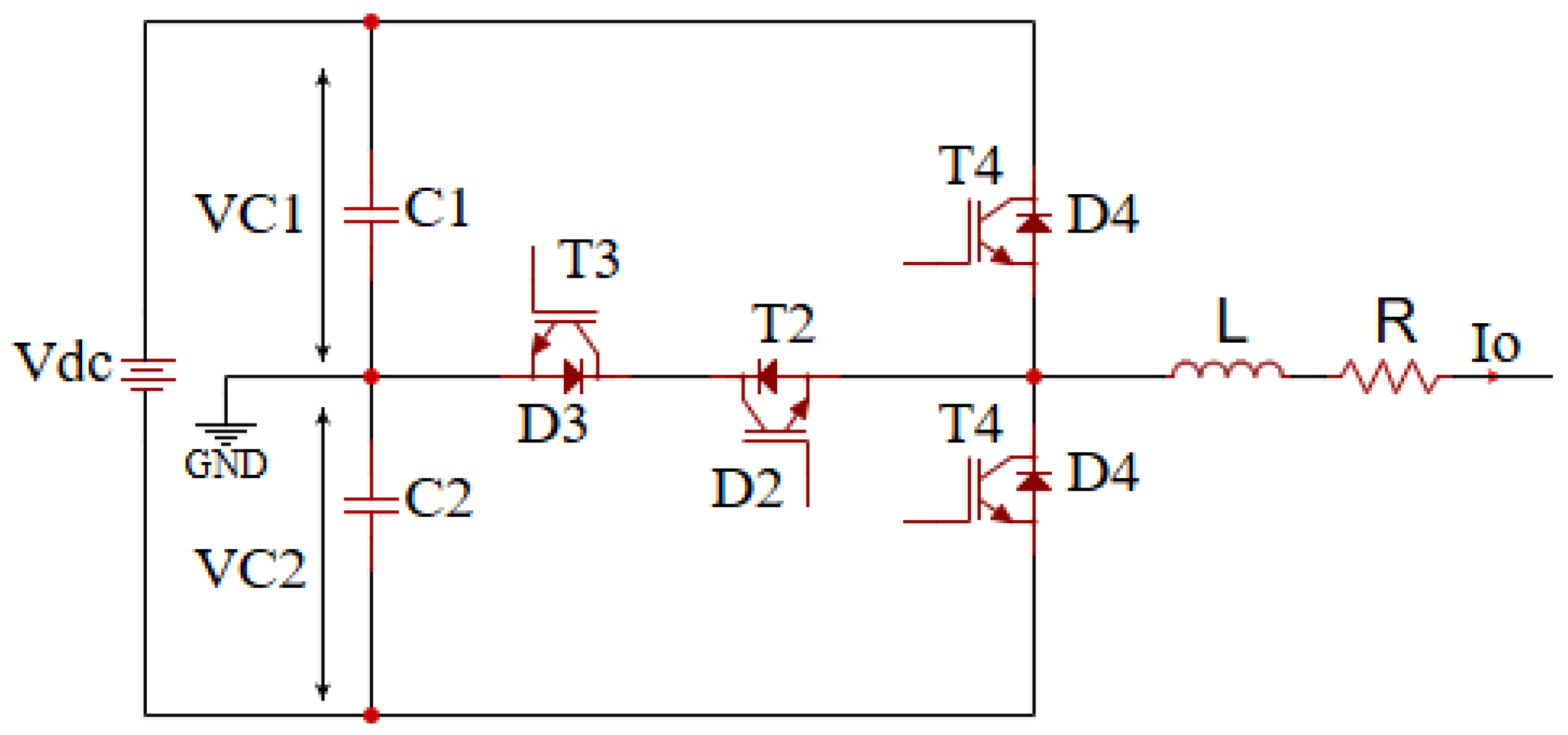
Achieving the three-level TNPC-IGBT inverter DC-link voltage balancing and load current symmetry allows for the evaluation of the single-leg equivalent circuit in the module’s analytical assessment.
Figure 6 is a schematic diagram of a single-leg equivalent circuit for the three-level TNPC IGBT inverter module under test. Each module leg consists of four transistors chips (T1, T2, T3, and T4), each paired with a freewheeling diode chip (D1, D2, D3, and D4). In this topology, under balanced operating conditions, the outer switches (SW1 and SW4) experience full DC-link voltage stress (Vdc), while the inner switches (SW2 and SW3) undergo only half the voltage stress (Vdc/2) due to their connection to the neutral point in the TNPC structure.
Table 3 distinctly outlines the detailed chip-level switching transitions for the TNPC inverter to facilitate accurate loss modeling during this balanced SVPWM operation. This table outlines the state changes, current flow directions, chips that activate and deactivate, and the resulting clamping or commutation actions for each possible switching event. The inverter’s switching transients are meticulously detailed for each operating condition by explicitly outlining these switching sequences, ensuring that the loss calculations accurately reflect the true device-level performance under balanced control. This comprehensive mapping, along with the recorded waveforms and energy scaling from the datasheet, provides a reliable basis for precise estimation of both switching and conduction losses.
In this IGBT module, the total power losses result from the conduction and switching losses of these semiconductor devices. To estimate the junction temperature (Tj), the power losses for each semiconductor component must first be calculated. Based on these losses and using the thermal model of the IGBT module switch, the junction temperature of each chip, along with the peak junction hotspot temperature value and position for the overall module, can be accurately estimated, as detailed in the following subsections.
3.1. TNPC-IGBT Module Transient Thermal Network
Transient thermal modeling of semiconductor devices can be performed employing different circuit-based and numerical techniques, with each presenting a balance between complexity and precision. Common approaches involve lumped RC networks like the Foster and Cauer models [
46,
47,
48], whereas numerical methods encompass finite difference and finite element techniques, thermal impedance curve fitting, and compact thermal models (CTMs). The Foster model employs curve fitting of observed thermal impedance and consists of parallel RC pairs with differing time constants, providing a simple and effective way to describe transient behavior. In contrast, the Cauer model arranges RC components in a ladder structure that reflects the device’s real thermal layers, offering better physical comprehension, as shown in recent research [
46,
48].
Numerical techniques (FDM and FEM) provide great precision for intricate shapes but require significant computational resources. CTMs achieve a compromise between numerical precision and reduced computational expense, rendering them perfect for real-time thermal observation. Among these approaches, the Foster model (shown in
Figure 7) is commonly utilized due to its simple depiction of heat transfer from junction to case via discrete RC components.
The increase in junction temperature caused by constant power loss is calculated as the combination of several first-order exponential responses as follows:
where
Tj(
t) is the junction temperature at time
t,
TC is the case temperature and is usually kept constant during testing,
Ploss is the average power loss dissipated in the chip,
Rth.i is the thermal resistance of the
i-th RC stage,
τi is the time constant of the
i-th RC pair and is equal to (
Rth.i.
Cth,i), and
k is the number of RC stages.
The exponential part in (4) is related to the transient thermal impedance,
Zth(
t), which reflects how quickly a device’s junction temperature rises after a power step and is crucial for RC Foster models and indicating dynamic thermal properties, where
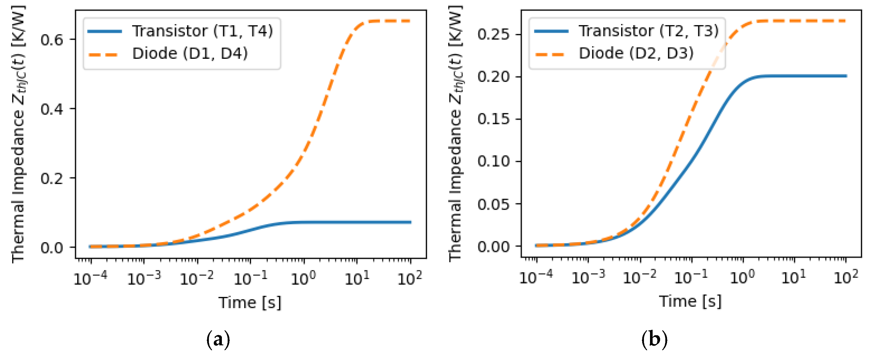
Figure 8 displays the simulated transient thermal impedance traits for the outer and inner switches of the SEMiX405TMLI12E4B IGBT module, using RC Foster data from the manufacturer’s datasheet [
42]. Diode chips in both inner and outer switches have a significantly higher thermal impedance than transistor chips, particularly for durations greater than 10 ms, slowing heat transfer to the case due to fundamental differences in chip metallization and thermal interface properties. Within the TNPC module chip configuration, the outer switches (T1 and T4) along with their diodes (D1 and D4) exhibit a higher thermal impedance compared to the inner switches (T2 and T3) and diodes (D2 and D3), a result of the module’s chip physical arrangement. Outer components undergo prolonged thermal conduction pathways via the DCB substrate and baseplate, while inner components enjoy reduced thermal distances and enhanced thermal connection with the heatsink. These differences in thermal impedance cause an irregular temperature distribution inside the module, affecting thermal efficiency and the device’s longevity due to heightened junction temperatures and potential thermal strain on external components.
From (4), at a constant case temperature, the temperature profile of the semiconductor chip junction can be evaluated using the transient thermal impedance features along with the instantaneous power loss profile (Ploss(t)) of each semiconductor chip. This power dissipation in the time domain includes both conduction and switching components, analyzed for each sampling interval according to the chip-level switching behaviors and conduction conditions.
The calculated Ploss(t) serves as a variable heat source applied at the junction node of each chip’s RC Foster network, while the case temperature (TC) is presumed to remain constant because of the cooling system. The junction temperature signal (Tj(t)) is derived by convolving the power profile with the thermal impedance of the chip (Zthjc(t)), reflecting the transient heat transfer properties. These Tj(t) profiles facilitate precise thermal monitoring for both the inner and outer devices of the TNPC module, illustrating the actual electrical–thermal stress endured by each chip.
3.2. TNPC-IGBT Module Chip-Level Conduction Loss Analytical Calculation
The main operational conditions that affect the overall conduction losses within the IGBT module include the load current (
Io), the voltage drop in the on state across the transistor (
Vceon), and the forward voltage drop across the diode (
VF). The conduction losses of an individual IGBT switch (
Pcon_IGBT) include the on-state losses of the transistor chip (
PconT) as well as the forward losses of the diode chip (
PconD); these can be represented as follows:
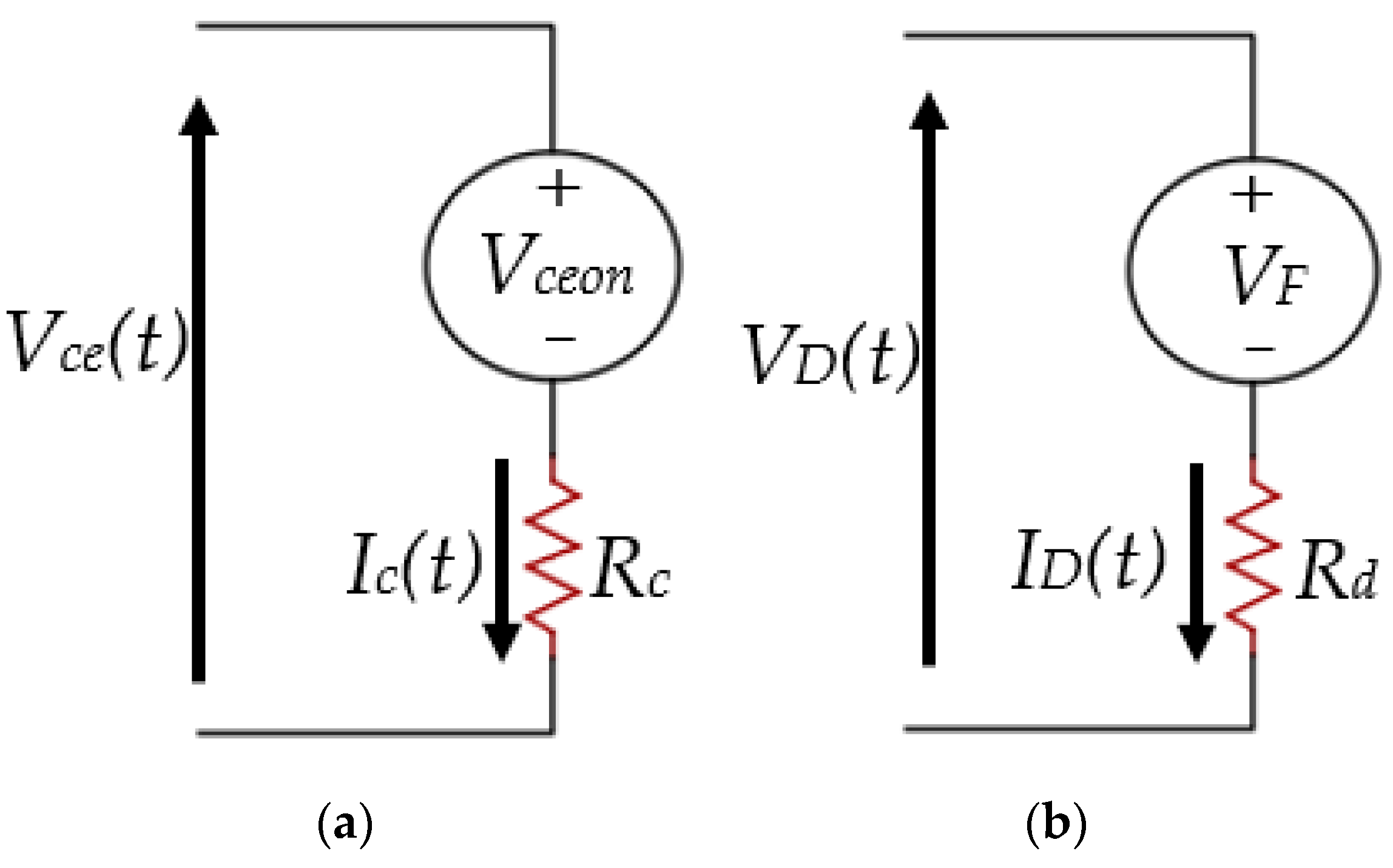
Figure 9a illustrates the equivalent circuit of the IGBT switch transistor chip when it is in the conduction state. By connecting a DC voltage source (
Vceon) in series, which represents the zero-current collector-emitter voltage in the transistor on state and the collector-emitter on-state resistance (
Rc), the conduction voltage of the transistor (
Vce(
t)) can be defined as follows:
The calculation of conduction voltage across the diode chip can be executed using the identical method and circuit equivalent depicted in
Figure 9b, leading to the following:
With the specified gate-emitter voltage (VGE = 15 V), the V-I characteristic datasheet for the chosen IGBT module’s transistors and diodes facilitates the derivation of the parameters Rd and Rc in (7) and (8). Once the conduction state resistances of the switch transistor and diode chips have been obtained, the diode and transistor chips’ conduction losses can be analyzed as follows.
3.2.1. For the Transistor Chips
For the IGBT switch, the instantaneous amount of conduction losses of the transistor chip is
And, over the switching period:
Substituting (9) into (10) gives
where
Ic_av and
Ic_rms refer to the average and RMS current values of the switch transistor chip (T), respectively.
In the IGBT module, every transistor (T) or diode (D) chip conducts a portion of the phase load current during its on state. In the three-phase TNPC-IGBT inverter, the RMS and average current values through the outer transistors (1 and 4) and inner transistors (2 and 3) during conduction can be determined based on the SVPWM modulation index (
m), maximum load current (
Io_max), and load power factor angle (
Φ), as expressed by the following:
For the three-level inverter, the SVPWM modulation index (
m) is calculated as follows:
where
Vo_Max is the maximum achievable voltage from the DC bus voltage.
3.2.2. For the Diode Chips
For the IGBT switch, the instantaneous amount of conduction losses of the diode chip is
And, over the switching period:
where
ID_av and
ID_rms refer to the average and RMS current values of the switch diode chip (D), respectively.
Similarly, in the three-phase TNPC-IGBT inverter, the RMS and average current values through the outer diodes (1 and 4) and inner diodes (2 and 3) during conduction can be determined based on the SVPWM modulation index (
m), maximum load current (
Io_max), and load power factor angle (
Φ), as expressed by the following:
3.3. TNPC-IGBT Module Chip-Level Switching Loss Analytical Calculation
The overall switching losses of the IGBT module (Psw_module) consist of two parts: the switching losses of the transistor chip and the loss during the diode chip’s reverse recovery. The evaluation of both parts can be analyzed as follows.
3.3.1. Transistor Chip Switching Loss Calculation
This switching loss takes place during the transition from the on state to the off state of the transistor and includes the turn-on losses as well as the turn-off losses. So, the transistor’s switching loss during a single switching cycle is
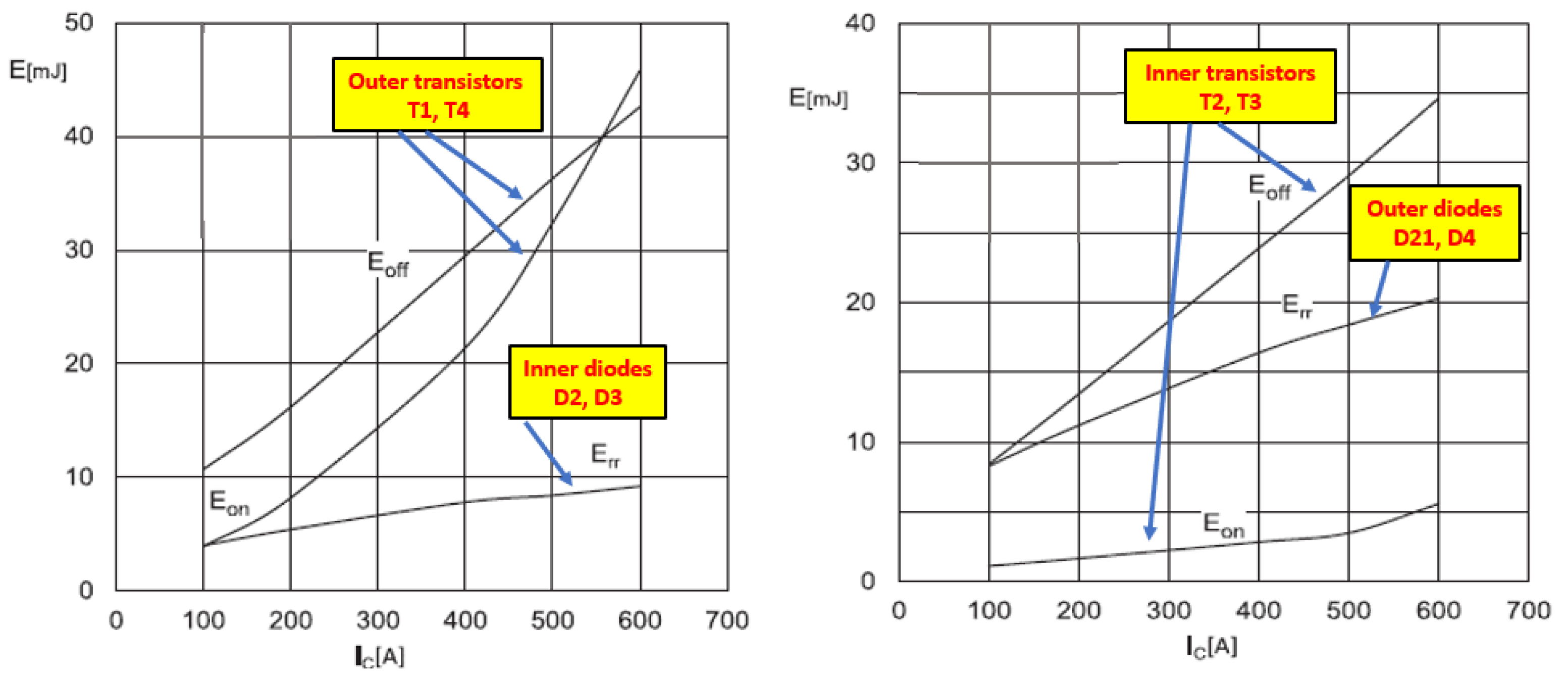
As shown in the datasheet characteristics provided in
Figure 10, the switching losses of the transistor are influenced by the energy necessary to switch on (
Eon) and switch off
(Eoff), which varies based on the transistor collector current, switching frequency, junction temperature, and input DC voltage, and can be represented as
Over the switching period, the transistor chip switching loss can be expressed as follows:
In the case of the three-level TNPC inverter with SVPWM control, the transistor chip’s switching losses for the module’s outer (T1 and T4) and inner (T2 and T3) transistor chips are derived as follows:
where
Inom and
Vnom represent the nominal load current and DC input voltage at which the characteristics in the datasheet are derived and
Vin denotes the input DC voltage (
Vdc) for the specific application and testing configuration.
Assuming the junction temperature remains constant during a single switching period,
Vin will also be constant during the switching interval at 450 V. Consequently, at the nominal junction temperature of 150 °C (the temperature at which the switching energy data are typically provided in the datasheet), the switching energy is primarily influenced by the variation in the
IC. Based on the device characteristics shown in
Figure 10, the turn-on (
Eon) and turn-off (
Eoff) switching energy values can be extracted for various loading scenarios (i.e., different values of I
C) at the nominal junction temperature,
Tj_nom = 150 °C.
To account for variations in junction temperature during operation, the switching energy at approximately the actual junction temperature,
Tj, can be corrected as follows:
where
α represents the typical temperature, the coefficient associated with IGBT switching losses. The coefficient
α quantifies the rise in switching energy for each °C increase in
Tj.
The manufacturer’s datasheet and application notes [
42,
49] for the SEMiX405TMLI12E4B module utilized in this work show that when the
Tj rises from 25 °C to 150 °C, the switching energy increases by about 30%. This results in a linear temperature coefficient (
α) of about 0.003 per degree Celsius.
3.3.2. Diode Chip Reverse Recovery Loss Calculation
The reverse recovery energy (
Err) of the diode also affects its reverse recovery loss (
PrrD). For the three-level TNPC inverter with SVPWM control, the reverse recovery losses associated with the module’s outer (D1 and D4) and inner (D2 and D3) diode chips are derived as follows:
Assuming that the junction temperature remains constant during a single switching period, the reverse recovery energy is influenced by the change in I
F. It can be determined using the device characteristics shown in
Figure 10 for both the inner and outer semiconductor chips.
The switching energy values used in this calculation, including
Eon, E
off, and E
rr, were obtained from the manufacturer’s datasheet [
42], which reflects standard double-pulse test (DPT) measurements performed at
Vin = 300 V, I
C = 400 A, and
Tj_nom = 150 °C. For the outer transistors (T1 and T4), the typical turn-on and turn-off energies are 21.4 mJ and 29 mJ, respectively; for the inner transistors (T2 and T3), they are 2.8 mJ and 23.9 mJ. The reverse recovery energy is about 16.4 mJ for the outer diodes (D1 and D4) and 8.5 mJ for the inner diodes (D2 and D3). To adjust the DPT results for the actual inverter operation, scaling factors for collector current, bus voltage, and junction temperature were incorporated into the switching loss computation as given in Equations (26)–(30).
After the chip-level losses modeling and to enhance the understanding of the stress distribution within the TNPC-IGBT module,
Table 4 outlines the voltage and current stresses that each semiconductor chip undergoes during conduction, switching, and reverse recovery under SVPWM operation. The values represent standard conditions derived from analytical modeling and are crucial for precise thermal and reliability evaluation.
4. MATLAB Simulation and Results
To validate the accuracy and effectiveness of the proposed control scheme and the developed mathematical thermal and loss model for the TNPC-IGBT module, the complete modeling of the three-phase, three-level TNPC-IGBT inverter based on the design specifications outlined in
Table 2 and with the optimal switching state for maintaining the DC-link voltage balance, along with the loss and thermal model, was executed in MATLAB software.
Figure 11 illustrates the simulated waveforms of the DC-link capacitor voltages (VC1 and VC2) under full load conditions (100 A, 200 V). The PI controller parameters were selected as K
p = 5 and K
I = 0.1. As shown, the implemented SVPWM control loop stabilizes VC1 around 227 V and VC2 around 223 V, resulting in a DC-link voltage imbalance of about 1.3% (less than the target percentage of 3%). Despite this minor and acceptable imbalance, the three-phase load current symmetry is well maintained, as demonstrated in
Figure 12, which promotes balanced electrical and thermal stress distribution across the inverter’s three legs.
Additionally, the analytical loss and thermal models of the module with different semiconductor chips were executed in MATLAB, considering loading conditions between 25 A and 100 A. The analytical findings for the switching, conduction, and peak junction hotspot temperature values along with their respective locations at the critical case temperature of 125 °C are shown in
Table 5. Furthermore,
Figure 13 displays the peak junction hotspot temperature values at different load currents; these findings demonstrate that regardless of the loading conditions, the junctions of the diode chip in the inner switches (D2 and D3) exhibit the highest junction temperature, reaching around 126.14 °C at a 25 A load current and approximately 131.20 °C at a load of 100 A.
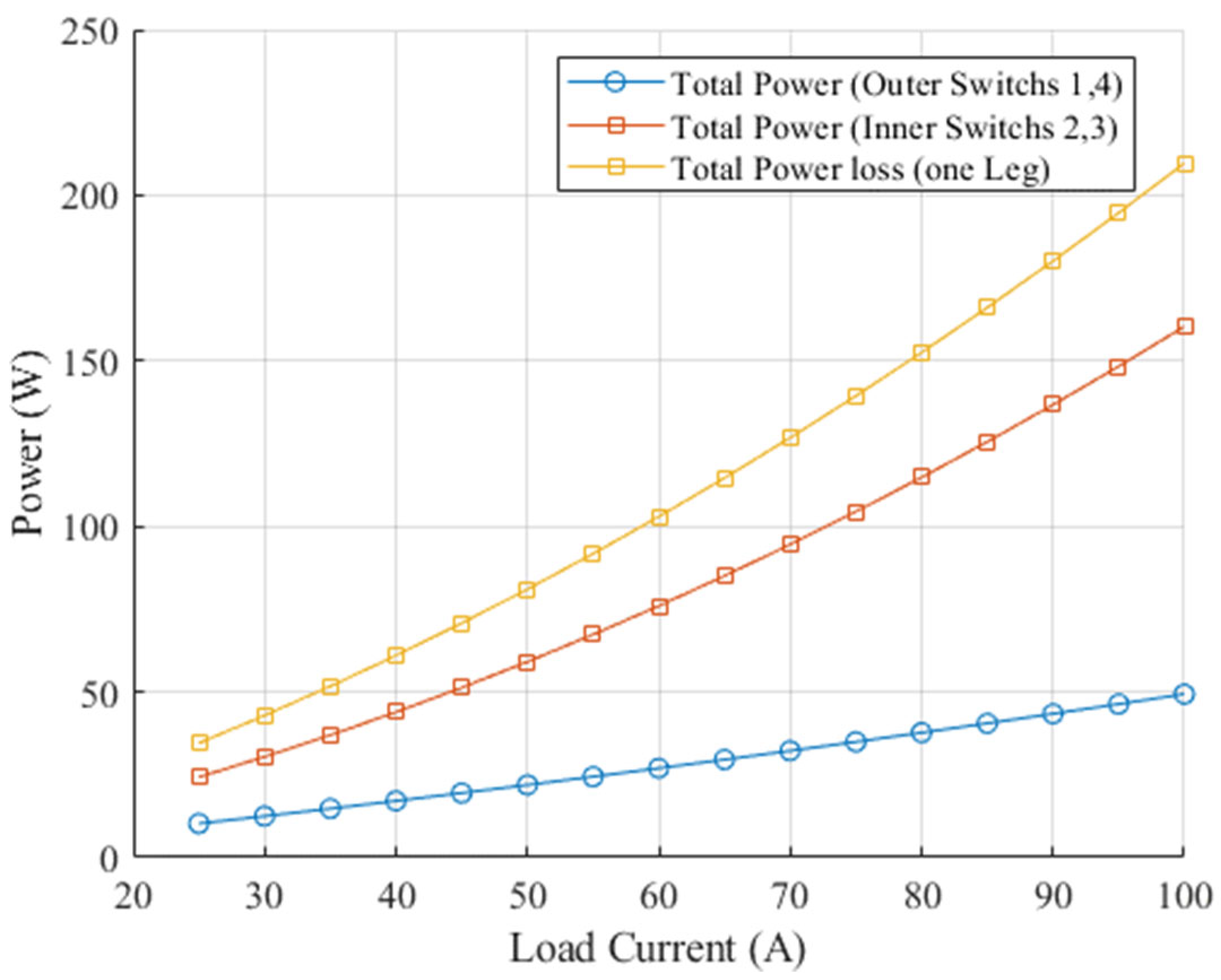
Figure 14 displays the results for the distribution of power loss throughout the inner (SW2 and SW3) and outer switches (SW1 and SW4) of a single leg in the IGBT module. It has been noted that when fully loaded at 100 A, the inner switches (SW2 and SW3) contribute roughly an average power loss of about 68%, whereas the outer switches (SW1 and SW4) contribute around 32% of the total power loss in the module. Additionally, the pie chart in
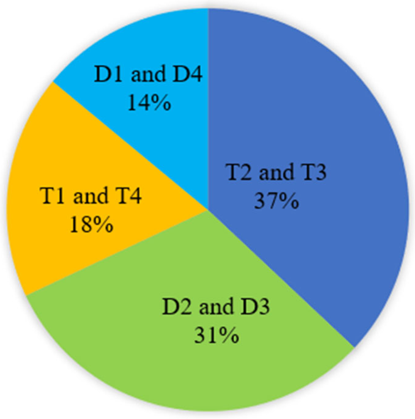
Figure 15 depicts the average distribution of power loss across various semiconductor elements within the employed IGBT module in a three-level T-type neutral-point-clamped (TNPC) inverter in the load range from 25 A to 100 A. It is noted that T2 and T3 account for the largest losses at 37%, with D2 and D3 following at 31%. T1 and T4 represent 18%, while D1 and D4 make up the smallest portion at 14%.
5. Model Validation and Experiments
5.1. SemiSel TNPC-IGBT Module Thermal Simulation
The SemiSel thermal simulation tool from Semikron was used for the thermal simulation and cross-verification of the calculated junction hotspot temperatures. SemiSel by SEMIKRON is a durable simulation tool designed for selecting and evaluating the performance of SEMIKRON power modules, including IGBTs, MOSFETs, and rectifiers [
50]. The benefit of SEMIKRON SemiSel is its dependable predictions, enabling precise evaluations of power losses and thermal performance. It assists in selecting the ideal IGBT module for specific applications and reduces design and testing time by offering pre-validation data, promoting cost savings by preventing the over- or under-specification of components; it also serves as a good benchmark to validate the analytical and experimental findings in previous research [
14,
51].
The SemiSel thermal simulation tool was utilized in this work to estimate the junction hotspot temperatures based on the specified nominal load condition, modulation strategy (SVPWM), and controlled heatsink temperature that maintains a constant case temperature during steady operation of the inverter. While the SemiSel tool is capable of managing different load scenarios, the particular configuration in this research signifies constant inverter performance under stable power and cooling settings. Additionally, the RC Foster thermal network was utilized with a specified constant power loss to present the steady-state inverter operation under defined load conditions. When subjected to ongoing losses, the Foster network attains a final thermal equilibrium that is equal to the total static junction-to-case thermal resistance times the power loss, added to the regulated case temperature. This allows for a direct comparison with the SemiSel simulation results, which utilized the manufacturer’s comprehensive internal thermal structure under identical steady-state power loss and boundary conditions.
For this purpose, the SEMIKRON IGBT module with part number SEMiX405TMLI12E4B was utilized to simulate the three-level TNPC inverter circuit in the SemiSel thermal software V6-2025, following the design specifications provided in
Table 2 and under different loading currents while maintaining the case temperature at its critical limit. To maintain the target module temperature (125 °C), the heatsink thermal stress was regulated in the simulation. The inverter control circuit used the SVPWM method with a 5 kHz switching frequency.
Under the specified load conditions of 100 A and 25 A, the module case temperature was maintained at 125 °C by regulating the heatsink temperature (T
s) during thermal simulation. The power loss distribution of the module’s various semiconductor parts was measured, as depicted in
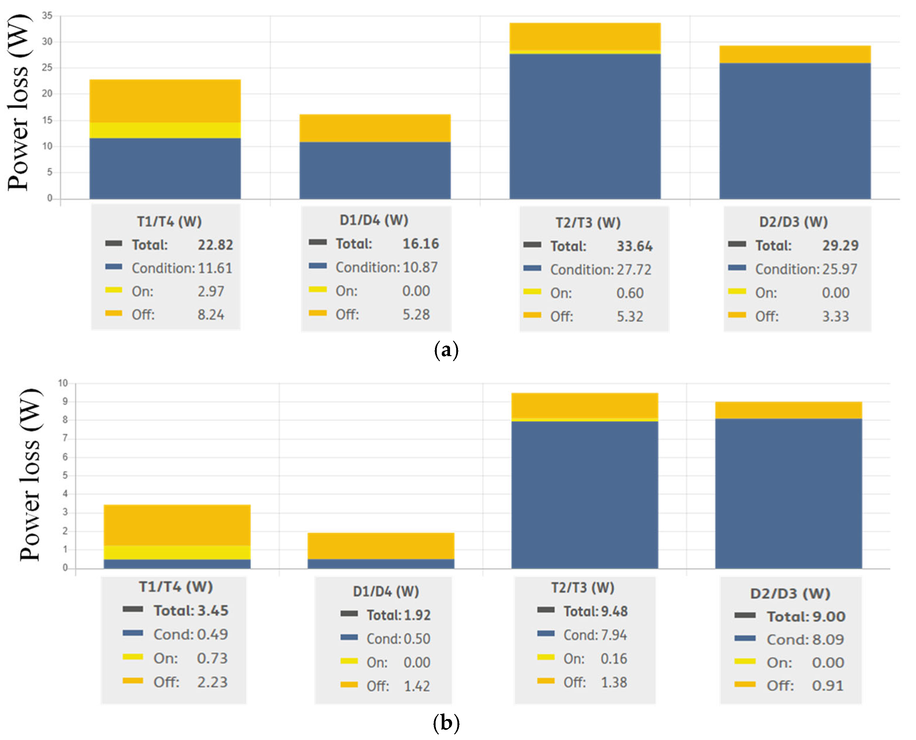
Figure 16a,b. This indicated that the module’s inner switches (SW2 and SW3) account for the highest amount of power loss at about 62.5%, while the outer switches (SW1 and SW4) account for about 37.5% of the module’s total power losses.
Additionally, the waveforms for the junction and heatsink temperatures of the transistor and diode chips in the inner and outer switches were simulated with load currents of 100 A and 25 A, as illustrated in
Figure 17 and
Figure 18. In the figures, the time is adjusted to 360° of one cycle of the output frequency. The peak junction hotspot temperature was observed to reach around 132.30 °C with 100 A and around 127.25 °C with 25 A at the diode chips of the inner switches (D2 and D3), as shown in
Figure 17b and
Figure 18b. Meanwhile, the lowest temperature stress occurred at the transistor chips of the outer switches (T1 and T4), with a value of about 126.51 °C at 100 A, as shown in
Figure 17c, and at the diode chips of the outer switches (D1 and D4), with a value of 125.26 °C at 25 A, as shown in
Figure 18d.
Moreover, under loading conditions ranging from 25 to 100 A, the thermal simulation process of the module at the critical case temperature was performed, and the conduction, switching, and overall module power losses were assessed, along with the module’s peak junction hotspot temperature and its location, as detailed in
Table 6.
The results from the Semikron SemiSel thermal simulation validate the anticipated performance of the TNPC-IGBT module and support the results from the developed loss and thermal model for the TNPC-IGBT module. In the three-level TNPC inverter, the outer switches (SW1 and SW4) experience the entire DC-link voltage but operate less frequently, leading to reduced switching losses. Inner switches (SW2 and SW3), functioning at a reduced voltage, toggle more often and consequently suffer from increased switching losses and thermal strain. This renders them thermally sensitive and highlights the requirement for improved cooling.
5.2. Experimental Verification
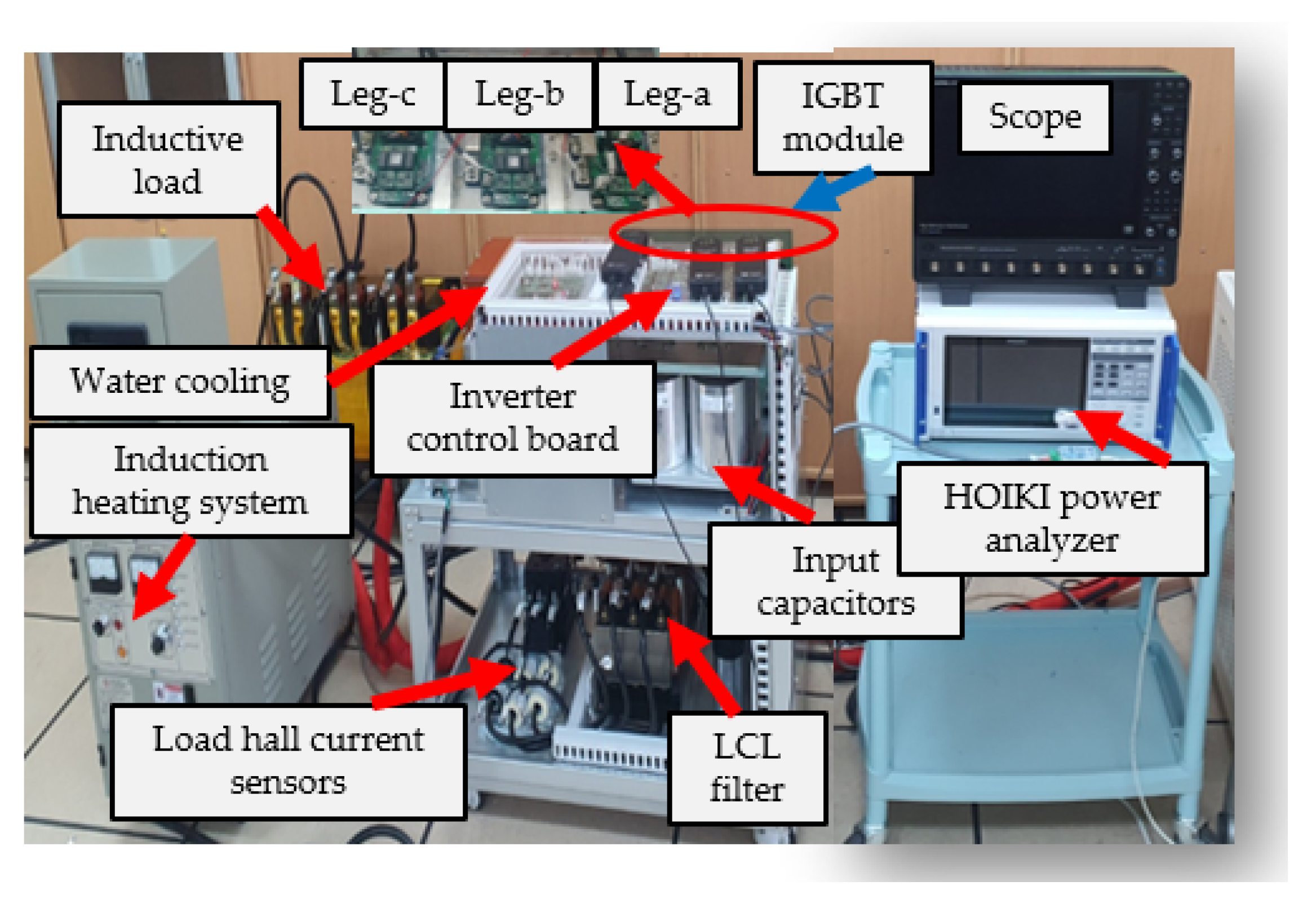
Figure 19 presents the experimental testing configuration of the three-phase inverter with the TNPC-IGBT module, constructed to validate the effectiveness of the designed SVPWM control strategy in maintaining the inverter DC-link voltage balance and to confirm the accuracy of the developed loss and thermal model of the TNPC-IGBT module in estimating the peak junction hotspot temperature (T
jpeak) and the module’s total power losses (P
loss-module).
The setup mainly consists of a three-level IGBT module, an induction heating system for case temperature control, an LCL filter to mitigate current harmonics, an inverter control circuit implemented using the DSP MCU TMS320 F28337D (Texas Instruments, Dallas, TX, USA), and a highly inductive load (R = 8.5 mΩ, L = 3 mH) with ratings of 100 A and 200 V. The HOIKI PW8001 (Hioki E.E. corporation, Ueda, Nagano, Japan) power analyzer was used to measure the module’s total power losses, and the OTP-M-100 fiber optic temperature sensor was employed for Tjpeak measurement at the position indicated by the developed model and SemiSel thermal simulation (at the inner diode chips).
The challenge in measuring the TNPC-IGBT module’s peak junction hotspot temperature under actual thermo-electrical stressing conditions is controlling and managing the module case temperature value during the electrical load application and the measurement process. In this work, a hybrid stress testing condition with highly electrical inductive loading and an induction heating system were used to measure the module’s peak junction hotspot temperature and total power losses under different loading conditions and at the critical case temperature of about 125 °C.
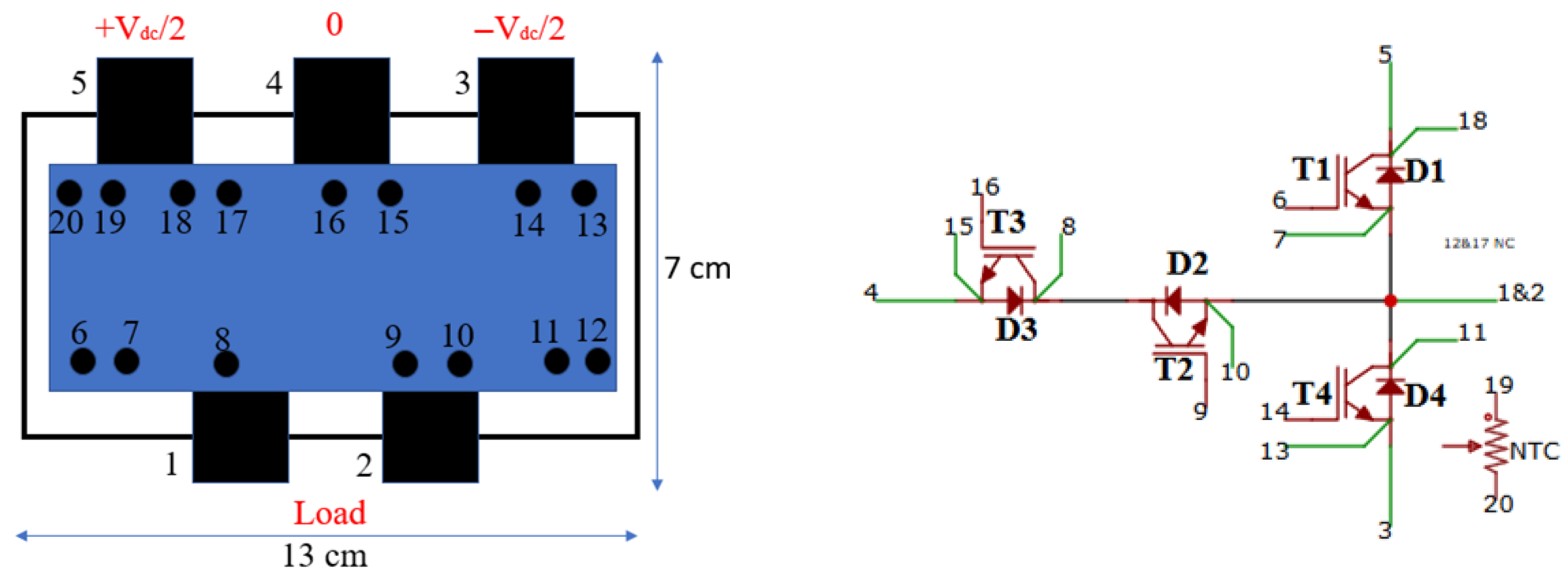
In the tested TNPC-IGBT module (SEMiX405TMLI12E4B), an NTC temperature chip was incorporated to serve as a proxy for monitoring the module’s case temperature status, as shown in
Figure 20a. The value of the negative temperature coefficient (NTC) resistance value, typically expressed as a function of temperature, can be calculated using the formula included in the module datasheet [
42], as given below:
where
R100 and
B100/125 are constants determined by the material properties of the NTC chip; they can be found in the datasheet [
42].
The general case temperature can be observed by measuring the NTC resistance (R
NTC) and referencing the integrated NTC’s resistance R-T characteristics.
Figure 20b illustrates the R-T profile of the integrated NTC sensor embedded in the Semikron SEMiX405TMLI12E4B IGBT module. During a measurement under a defined electrical load, the case temperature of all three inverter legs is maintained using an induction heating system with a water-cooling system.
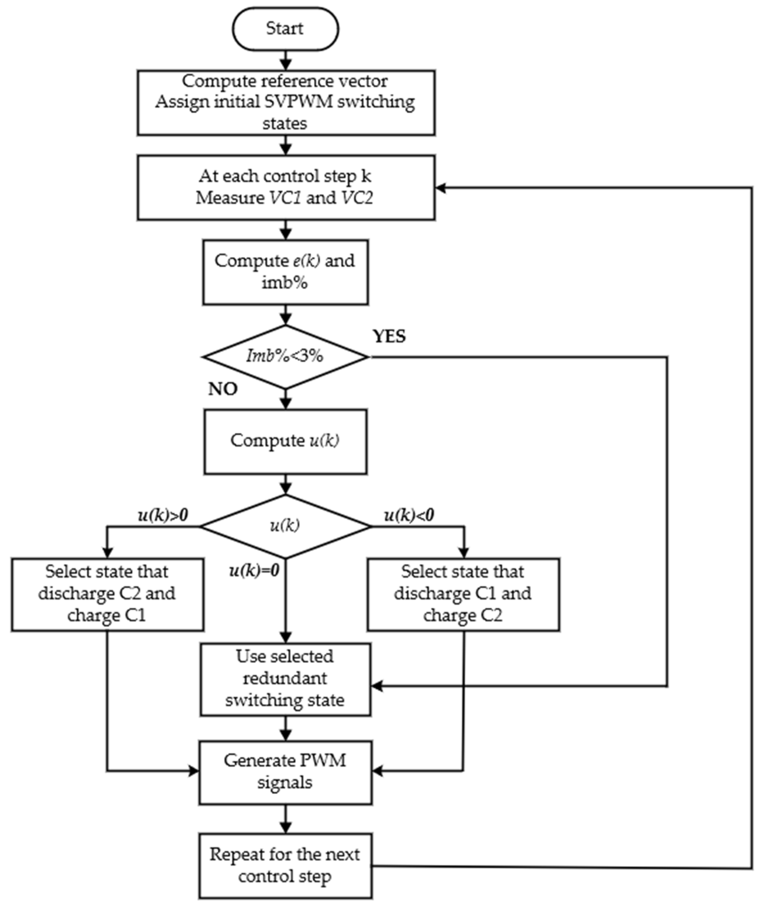
A DC power supply of 450 V and SVPWM control signals at 5 kHz were applied to the inverter circuit. Firstly, a highly inductive load was utilized to test the thermal performance of the IGBT module at high currents of up to 100 A. However, before monitoring the thermal performance of the IGBT module switches with the developed system, the voltage across the input capacitances was sensed and fed back to the designed control circuit. This feedback was used to modify the SVPWM switching state sequence based on the imbalance percentage, ensuring that the DC-link voltage imbalance remained below 3%. This process guaranteed load current balancing and uniform stress distribution across the module’s three legs.
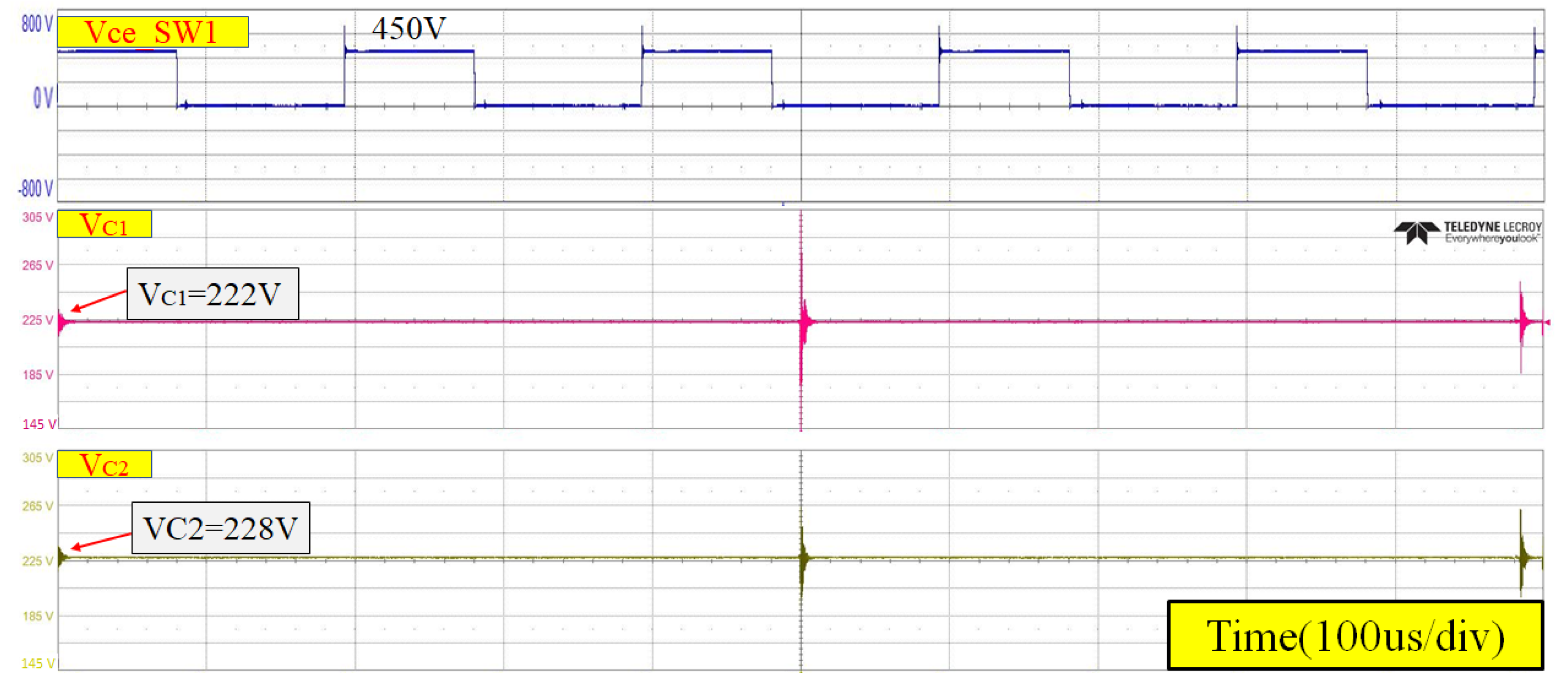
Figure 21 illustrates the experimental waveforms of the collector-emitter voltage (Vce_SW1) across the outer switch (SW1) and the voltages of the input capacitance (VC1 and VC2). This shows that the inverter control system maintained the DC-link voltage imbalance within the desired range, with VC1 and VC2 measured at 222 V and 228 V, respectively, resulting in an imbalance percentage of approximately 1.33%.
Additionally,
Figure 22 shows the experimental waveforms of the load currents at 100 A and the RMS levels of the three phases, which indicate the well-magnitude and phase balance of the three-phase currents in the three-level TNPC-IGBT module under test. This indicates symmetrical operation and uniform voltage stress distribution over the module’s three legs, enabling the monitoring of only one leg of the IGBT module, which facilitates analysis and reduces the complexity of the experimental setup and measurements.
After stabilizing the DC-link voltage and balancing the load current, the induction heating system controls the heatsink to keep the case temperatures of the three module legs close to 125 °C. Case temperature readings are taken using the built-in NTC sensor. A HOIKI PW8001 power analyzer tracks the module’s input and output power to determine the overall power losses. Furthermore, the junction temperature of the inner diode chips is assessed during operation with one of the module terminals left open.
Figure 23a illustrates the experimental measurements of the IGBT module’s input-output power with different load currents ranging from 25 A to 100 A. Additionally,
Figure 23b presents the module’s power losses and the peak junction hotspot temperature (T
jpeak) values at the various load currents, indicating a peak junction hotspot temperature of approximately 131.40 °C at the inner diode chip position under a 100 A load current (developed model estimated 131.20 °C) and about 126.66 °C at a 25 A load current (developed model estimated 126.14 °C).
The detailed values of the experimental results for the module’s total power losses, as well as the module’s peak junction hotspot temperature at load currents of 25, 50, 75, and 100 A, are provided in
Table 7. The DC-link capacitor losses due to the ESR were included in the calculation and subtracted from the total input power to the module. These losses were minimal, totaling less than 1 W at the full load current of 100 A.
The curves illustrated in
Figure 24 represent the experimental data of the peak junction hotspot temperature (T
jpeak) as the module case temperature varies from 55 °C to approximately 125 °C under four distinct load current scenarios. It is noted that, with an increase in case temperature, T
jpeak also rises for all load currents. Increased load currents cause more power loss, resulting in elevated junction temperatures. For instance, at a case temperature of 55 °C, T
jpeak is 57.35 °C at 25 A but increases to 62.79 °C at 100 A. Moreover, at a case temperature of 125 °C, T
jpeak is 126.66 °C for 25 A, while it attains 131.4 °C for 100 A. This trend emphasizes the influence of thermal stress on semiconductor devices. Efficient cooling and thermal regulation are crucial to avoid high junction temperatures, ensuring the reliability and lifespan of power electronic devices such as IGBTs.
6. Comparative Evaluations of the Results
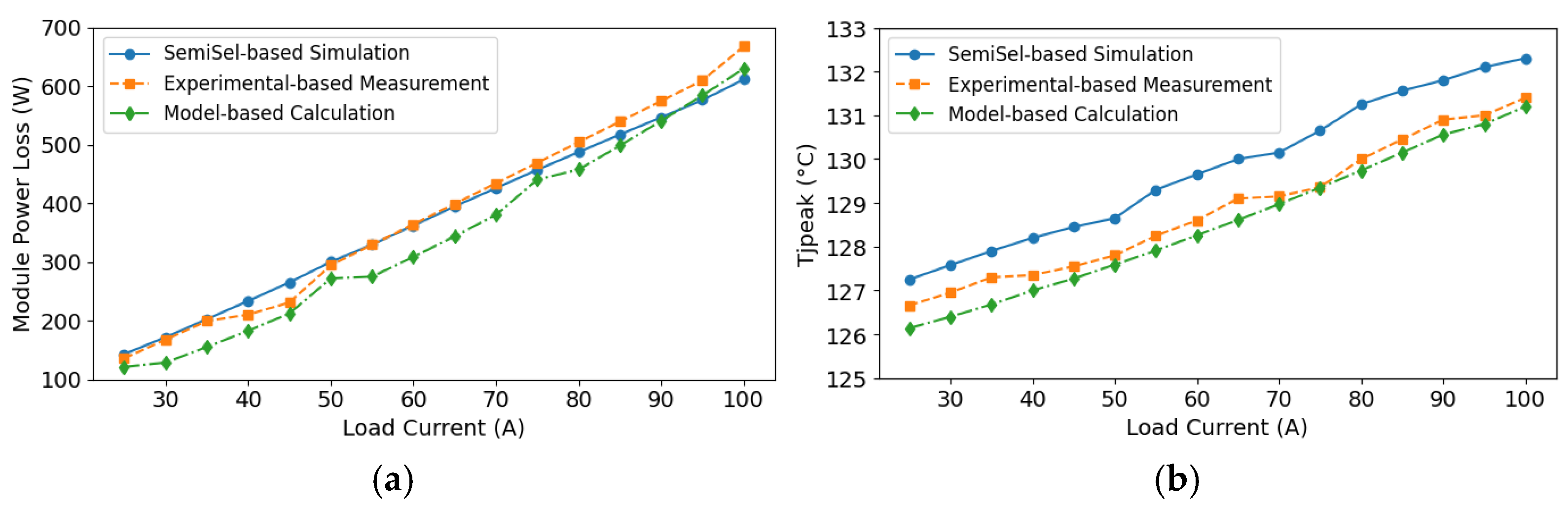
This section presents a comparative assessment of the power losses and peak junction hotspot temperature values derived from the proposed analytical analysis and experimental measurements, together with the thermal simulation outcomes from the SemiSel simulation benchmark provided by Semikron. It aims to demonstrate the accuracy and applicability of the proposed techniques for estimating power loss and junction temperature in the three-level TNPC-IGBT module.
Figure 25a displays the total power losses of the module obtained from analysis, experimental results, and simulation-based SemiSel for the employed TNPC-IGBT inverter module across various load currents. It is clear that the experimental results closely match the SemiSel benchmark across the entire spectrum of load currents, exhibiting slight variations. This indicates that the proposed experimental technique effectively validates the SemiSel simulation results for power loss estimation. Additionally, the analytical method slightly underestimates the power losses compared to the SemiSel benchmark, particularly at lower load currents. However, the discrepancy diminishes as the load current increases, with the analytical results converging toward the SemiSel values. Overall, the SemiSel simulation demonstrates significant alignment with the experimental findings, validating it as a reliable benchmark. The analytical approach, although following a similar trend, tends to underestimate power losses at lower currents but improves its accuracy at higher currents, thereby becoming reasonably consistent with the SemiSel predictions.
Moreover,
Figure 25b illustrates the peak junction hotspot temperature (T
jpeak) of the module derived from analytical modeling and experimental testing, in conjunction with SemiSel simulation results, demonstrating that experimental data closely align with the SemiSel simulations, with the variation at any load condition remaining below 1 °C. This correlation confirms the reliability of both techniques in predicting the IGBT’s thermal characteristics. The analytical model consistently undervalues T
jpeak due to the approximations used in identifying the operating point and extracting parameters from the module’s datasheet. These simplifications result in minor discrepancies from actual conditions that influence the module power loss calculation and, consequently, the junction temperature value. Nonetheless, the general trend persists uniformly across all methods, validating the dependability of the analytical technique for estimation needs.
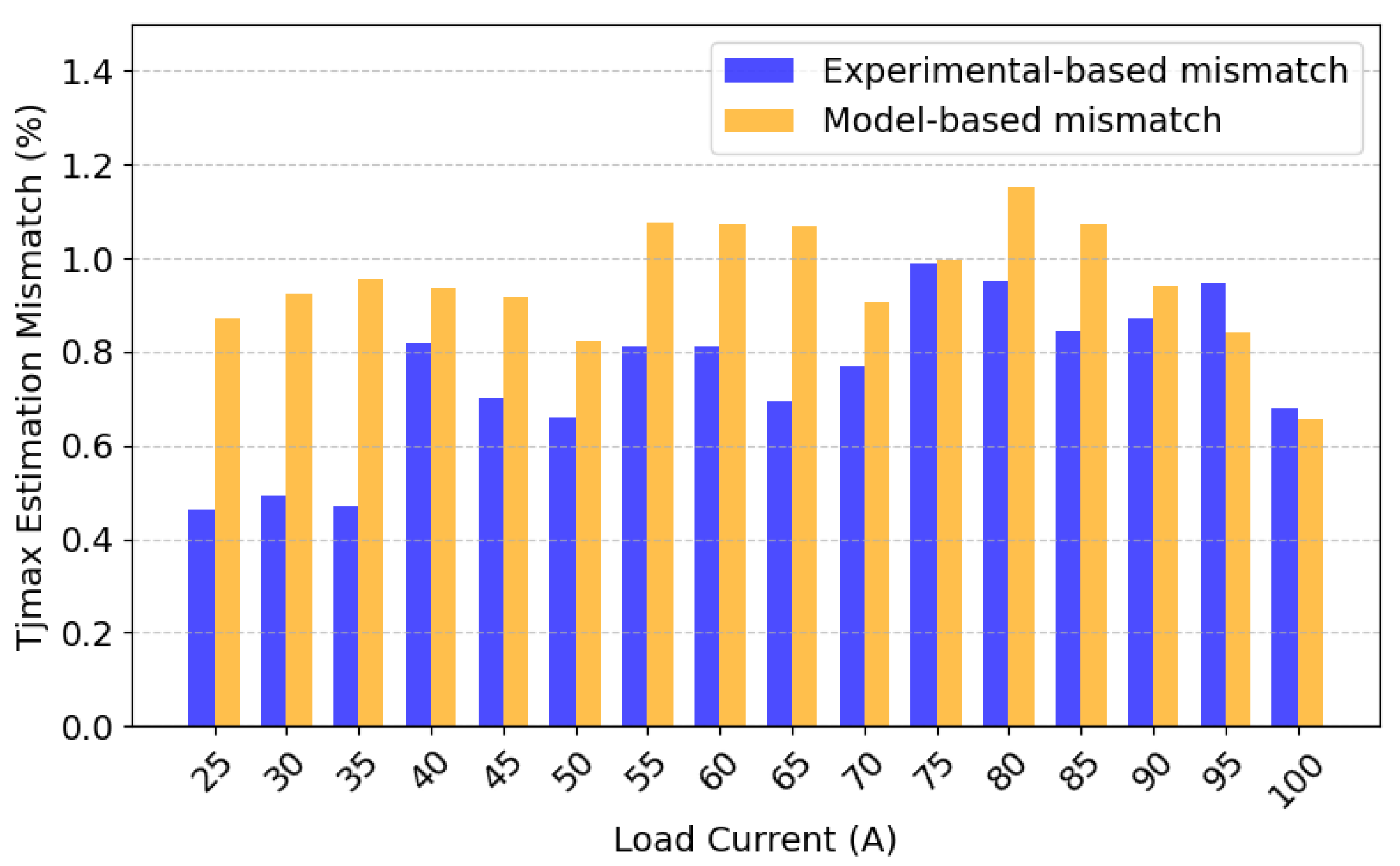
To deliver precise insights into the accuracy and precision of each method for estimating junction temperature, the graph in
Figure 26 displays the percentage of mismatch for all calculations under loads ranging from 25 A to 100 A, using SemiSel as a benchmark. The experimental mismatch remains less than 1%, verifying its close correlation with the simulation. The analytical discrepancy slightly increased due to the assumptions made in determining the operating point and deriving parameters from the characteristics in the module datasheet. The highest analytical deviation (1.14%) was observed at 80 A. Nevertheless, both techniques maintained a steady trend, illustrating their dependability for estimation.
While the SemiSel tool provides an extremely accurate benchmark for SEMIKRON modules, it is proprietary and exclusively relevant to SEMIKRON products. In comparison, the proposed chip-level electro-thermal model, as well as the developed hybrid stress testing setup, is universal and independent of vendors, allowing it to be used with any IGBT module from different manufacturers lacking equivalent simulation tools of similar quality. The close collaboration with SemiSel confirms the proposed method’s precision and relevance to broader industrial and research uses. In summary, the findings confirm that the analytical loss modeling and the proposed hybrid testing experimental measurements serve as reliable methods for estimating junction temperatures in power semiconductor devices operating at the critical thermal limit with high accuracy.
The main contributions of this research can be outlined as follows:
A detailed chip-level electro-thermal model was developed for the three-level TNPC inverter that resolved each IGBT and diode chip while factoring in the actual datasheet specifications of the module and the practical electrical and thermal operating conditions of the inverter.
The proposed model accurately predicts local thermal hotspots and stress inconsistencies by integrating device-specific switching energy extraction, actual switching gate signals, and an RC Foster thermal network.
A comprehensive hybrid stress experimental setup was established to directly assess total module power losses and confirm the computed peak junction hotspot temperature through a fiber-optic temperature sensor in realistic operating conditions.
Using the accurate SemiSel simulation tool for SEMIKRON modules, the model’s accuracy was verified, demonstrating outstanding correspondence and confirming the recommended approach for a reliable thermal performance assessment of multilevel IGBT modules.
The developed model and experimental testing configurations are general and suitable for various IGBT modules and do not require specialized thermal simulation assistance, unlike proprietary vendor-specific software.
Overall, this study provides a valuable, flexible method for improving lifetime estimation, reliability evaluation, and thermal design of advanced multilayer inverter systems functioning in extreme heat conditions.
7. Conclusions
This study presents a detailed electro-thermal modeling and validation framework for accurately predicting the peak junction hotspot temperature in TNPC-IGBT modules utilized in three-level balanced inverters working under extreme thermal conditions. A comprehensive loss model, utilizing real datasheet parameters and circuit specifications, was developed to calculate the power dissipation in separate semiconductor chips. Combined with comprehensive transient RC Foster thermal network modeling, this method facilitated accurate forecasting of chip-level junction temperatures and detection of the module’s thermal hotspot within the module.
To validate the developed modeling, a hybrid stress experimental configuration was established, facilitating direct measurement of power losses and junction temperatures under managed thermal and electrical stress. The incorporation of a DC-link balancing control circuit along with an induction heating system guaranteed an even stress distribution and improved measurement reliability.
Validation against the SemiSel thermal simulation benchmark showed a comparative analysis with excellent accuracy, recording peak junction hotspot temperature variations of less than 1.15% for the analytical model and below 1% for the experimental approach. This validated that the proposed electro-thermal model, backed by hybrid experimental verification, offers a dependable and precise method for assessing the thermal performance of IGBT modules under realistic extreme-temperature operating scenarios. The proposed estimation techniques are appropriate for improving the design, reliability evaluation, and thermal control of power semiconductor devices in high-performance multilevel inverter systems.


