Article

Improvement of Positive and Negative Feedback Power Hardware-in-the-Loop Interfaces Using Smith Predictor

by
Lucas Braun
*,
Jonathan Mader
,
Michael Suriyah
and
Thomas Leibfried
Institute of Electric Energy Systems and High-Voltage Technology (IEH), Karlsruhe Institute of Technology (KIT), 76131 Karlsruhe, Germany
*
Author to whom correspondence should be addressed.
Energies 2025, 18(14), 3773; https://doi.org/10.3390/en18143773
Submission received: 10 June 2025 / Revised: 9 July 2025 / Accepted: 14 July 2025 / Published: 16 July 2025

Abstract

Power hardware-in-the-loop (PHIL) creates a safe test environment to connect simulations with real hardware under test (HuT). Therefore, an interface algorithm (IA) must be chosen. The ideal transformer method (ITM) and the partial circuit duplication (PCD) are popular IAs, where a distinction is made between voltage- (V-) and current-type (C-) IAs. Depending on the sample time of the simulator and further delays, simulation accuracy is reduced and instability can occur due to negative feedback in the V-ITM and C-ITM control loops, which makes PHIL operation impossible. In the case of positive feedback, such as with the V-PCD and C-PCD, the delay causes destructive interference, which results in a phase shift and attenuation of the output signal. In this article, a novel damped Smith predictor (SP) for positive feedback PHIL IAs is presented, which significantly reduces destructive interference while allowing stable operation at low linking impedances at V-PCD and high linking impedances at C-PCD, thus reducing losses in the system. Experimental results show a reduction in phase shift by 21.17° and attenuation improvement of 24.3% for V-PCD at a sample time of 100 µs. The SP transfer functions are also derived and integrated into the listed negative feedback IAs, resulting in an increase in the gain margin (GM) from approximately one to three, which significantly enhances system stability. The proposed methods can improve stability and accuracy, which can be further improved by calculating the HuT impedance in real-time and dynamically adapting the SP model. Stable PHIL operation with SP is also possible with SP model errors or sudden HuT impedance changes, as long as deviations stay within the presented limits.

1. Introduction

Power hardware-in-the-loop (PHIL) enables the analysis of interactions between physical hardware under test (HuT) and a simulation in a safe laboratory environment. For example, solar inverters [1,2,3], cables [4], grid protection systems [5,6], and energy storage systems [7] serve as HuT. The system of interest can be models of DC microgrids [8] or other digital twins, such as benchmark networks [9,10]. These models are simulated in real-time on appropriate digital real-time simulators (DRTSs) with defined sample times. For phasor simulations and models that do not require such a high level of accuracy, a larger sample time can be chosen [11], which is typically between 1 and 10 ms [12]. Electromagnetic transient (EMT) simulations and models that require a higher level of accuracy are calculated with sample times in the microsecond range. In addition to the more expensive DRTS, less expensive PHIL setups, but with longer sample times, can be realized based on programmable logic controllers, microcontrollers, or PCs [11,13,14].
To connect the real HuT to the simulation, a power amplifier (PA) is used. The PA typically receives its setpoint via an optical link (OL) or analog interface, which, depending on the PHIL interface algorithm (IA), can either be a current or voltage signal that is calculated by the DRTS. To account for the behavior of the HuT, the voltage and current at the HuT are measured either by additional measurement systems or by measurement systems integrated into the PA and are subsequently fed back into the simulation. The system time delay consists of two components: the sample time and the time needed for communication, conversion, and measurement of signals. Hence, lower communication latency is preferred, making OL communication favorable due to its lower latency [11,15]. Because PHIL setups are mixed-signal systems, the sum of the continuous time delays must ideally be smaller than the sample time of the DRTS [16], to ensure that the total closed loop time delay can be assumed as twice the simulation DRTS sample time [17,18]. Otherwise, the total system time delay can consist of three or more discrete sample times, which may result in lower stability and accuracy. In practice, it is challenging to model reality accurately with a PHIL setup due to time delays and non-ideal transmission behavior caused by the low-pass behavior of the PA, DRTS discretization effects, and other parasitic effects, as shown in [10,19]. For a more accurate stability analysis of the system, it is necessary to determine the closed loop and all system parameters as accurately as possible [20].
In addition, an appropriate IA must be selected to match the setup, where a distinction is made between the voltage-type (V-) and current-type (C-) IA, which describes the setpoint for the PA. In [12,21], the ideal transformer method (ITM) is referred to as the most commonly used IA because it is easy to implement and provides a high level of accuracy. However, it is shown in [19,21] that the ITM quickly reaches its stability limit, which is caused by two factors: the ratio between the simulated impedance and the actual HuT impedance, as well as the time delay and parasitic effects of the system. The stability and the scope of the setup can be improved by introducing a first-order low-pass filter (LPF) in the measurement feedback, which is shown in [10,22]. However, this reduces the bandwidth, dynamics, and accuracy of the PHIL setup. In [23], a coupling method is presented, which was transferred to PHIL in a modified form and is known as partial circuit duplication (PCD). In [12,24], the method is used for large-scale systems when the HuT is bonded to the simulated system through a linking impedance. The PCD method has the advantage that it is theoretically always stable and the gain margin (GM) increases with increasing linking impedances at V-PCD and decreasing linking impedance at C-PCD. However, this results in increased system losses, as well as lower accuracies [25]. In all IAs, there is a trade-off between dynamics, bandwidth, accuracy, scope, and, most importantly, the stability of the system [25].
The effect of time delay on system stability and accuracy depends on the IA used [26,27]. For negative feedback control loops, such as V-ITM and C-ITM, the stability and accuracy decrease for higher time delays. In contrast, for positive feedback control loops, such as V-PCD and C-PCD, phase shift and attenuation increase with time delay due to destructive interference, which significantly reduces accuracy. These negative effects also occur in other, more stable IAs, such as the damping impedance method (DIM) and the transmission line model (TLM) presented in [21,25,28], and increase with larger time delay. For both categories of IAs, additional noise perturbation in the control loop, such as measurement noise, further reduce stability and accuracy. Hence, this paper aims at developing methods that compensate the time delay of the system to ensure more accurate PHIL simulations. To achieve this, a method based on the Smith predictor (SP) is proposed. The SP is a method from control theory that can be used to compensate time delay and its negative effects in systems. First applications of SP-based approaches can be found in [29,30], where an SP is applied to V-ITM. In [29], an SP circuit for this IA is presented. The improvement of stability is validated and a real-time sliding discrete Fourier transform measurement of the HuT impedance is added.
This article highlights the novelty of an advanced filtered SP developed for positive feedback PHIL setups, which represents a significant advancement for the V-PCD and C-PCD IAs, by reducing the destructive interference. This indicates a significant reduction in both phase shift and attenuation. This new damped SP compensates the time delay and also enables practical, more accurate, and stable operation of the PHIL setup at low linking impedances for V-PCD and high linking impedances for C-PCD, thereby reducing power losses in the system. The article also demonstrates how an SP significantly improves system stability—by approximately a factor of three—for systems with negative feedback control loops, by compensating the time delay and ensuring higher accuracy. First, the SP is applied to the V-ITM, which is already established in [29]. Furthermore, as a novelty, this article shows the first application of an SP in the C-ITM. The article shows how real-time impedance calculation of the passive HuT using measured values and dynamic adaptation of the SP model significantly improves stability and maintains a nearly constant GM.
This article is structured as follows: Section 2 provides a general overview of the system time delay composition and the operating principle of the PCD and ITM IAs. Section 3 derives the mathematical functions and block diagrams of the SP for V-ITM, C-ITM, V-PCD, and C-PCD, which compensate the system time delay. The advanced damped SP for V-PCD and C-PCD with positive feedback is presented. The simulation results are shown and analyzed in Section 4. In Section 5, experimental results are presented to validate the simulation results and demonstrate the enhanced stability and accuracy of the practical PHIL setups. Finally, Section 6 offers the conclusion and provides a brief outlook.

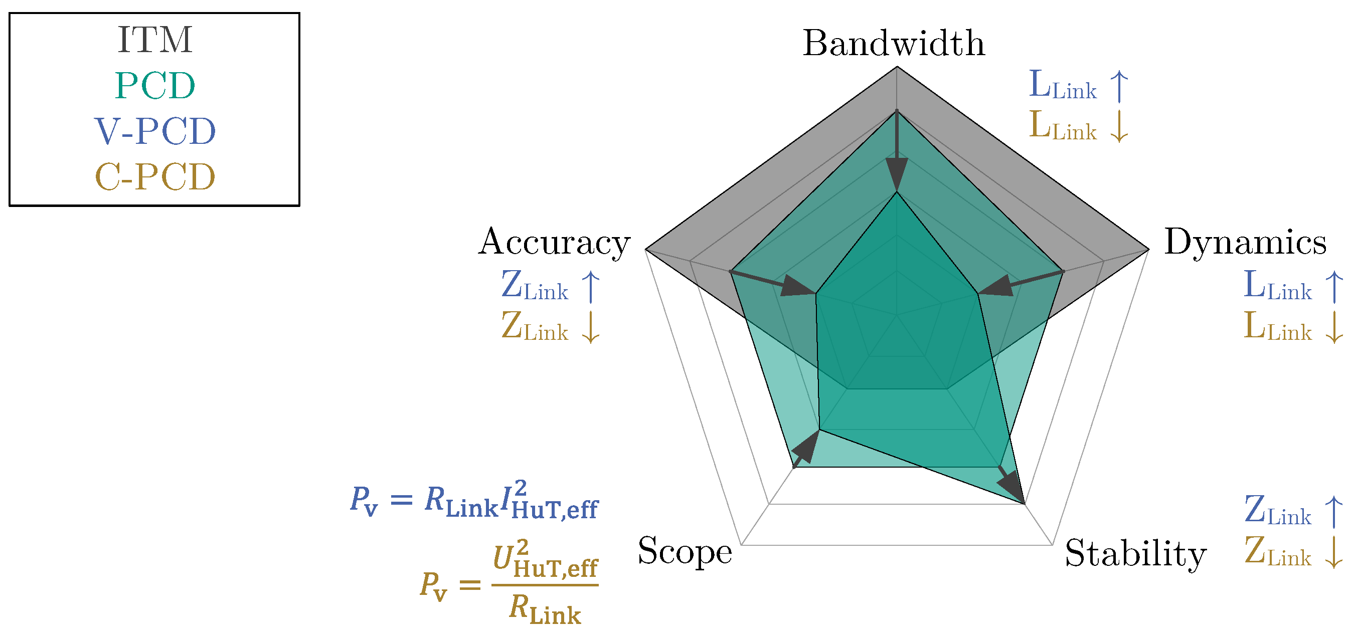
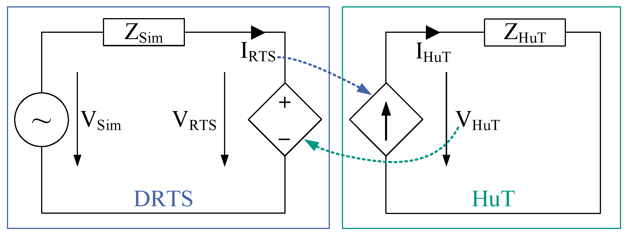
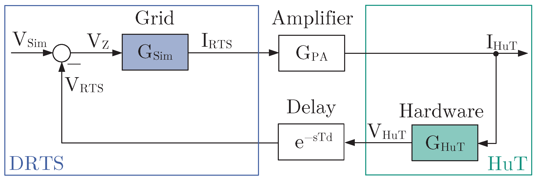
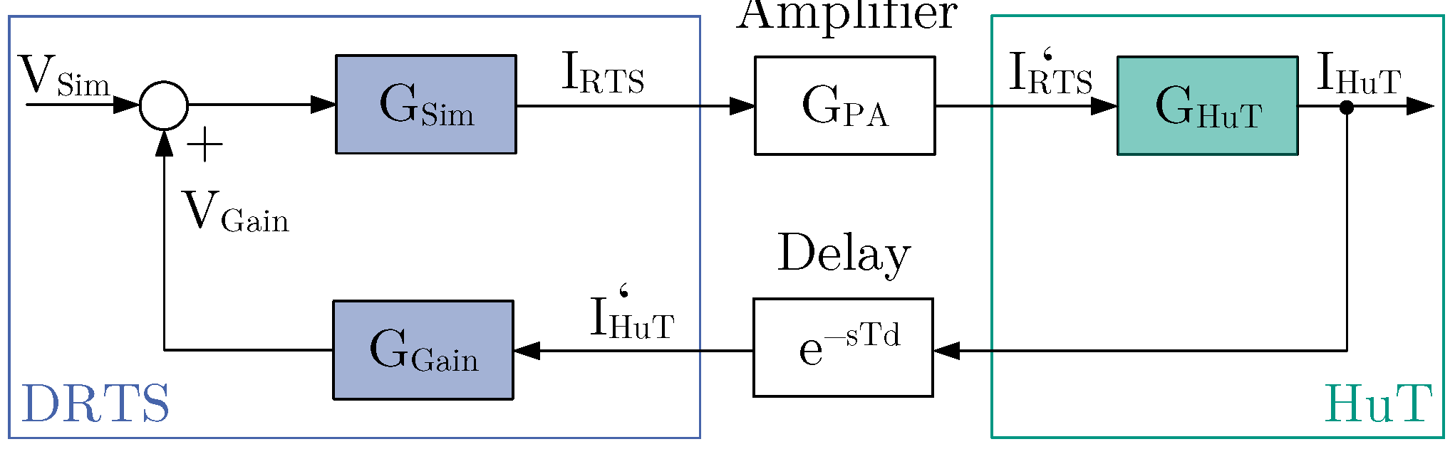
2. Interface Algorithms

The most common and straightforward IAs are the ITM and PCD. A qualitative visual comparison of the two IAs is shown in Figure 1, and they are examined in more detail in the following sections. A distinction is made between V-IA and C-IA, which are based on voltage and current setpoints, respectively. Depending on the IAs, the measured HuT current or voltage is fed back into the simulation.
The continuous open loop time delay T d , Cont of each IA consists of the simulation sample time T DRTS , the digital-to-analog conversion time T D / A , the analog-to-digital conversion time T A / D , the measurement time T Meas , and additional time delays T Rest :
T d , Cont = T DRTS + T D / A + T Meas + T A / D + T Rest
However, since PHIL is a coupling of a discrete and continuous system, the closed loop time T d , which is here important for the stability, equals twice the DRTS sample time if the continuous system is fast enough:
T d = 2 · T DRTS = ^ z 2

2.1. Ideal Transformer Method

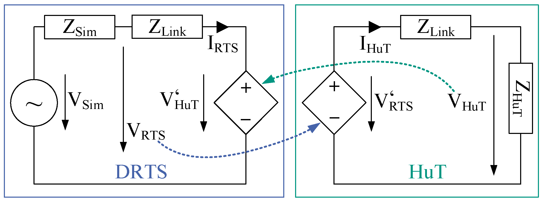
2.1.1. Voltage-Type ITM

The IA based on the V-ITM is illustrated in Figure 2. The voltage V RTS across an ideal controlled current source is calculated in the simulation and transmitted to a PA as a setpoint, which is presented as a controlled voltage source. Depending on the actual HuT impedance Z HuT , a current I HuT flows. This current is measured and fed back into the simulation. The voltage V RTS is calculated in the DRTS depending on the calculated simulation voltage V Sim and the simulated impedance Z Sim , which depends on the simulated network. The block diagram of the control circuit is shown in Figure 3, the parameters of which are discussed next.
The transfer function of the simulation G Sim includes the simulated inductance L Sim and resistance R Sim :
G Sim = Z Sim = s L Sim + R Sim = s 620 μ H + 22.18 Ω
The transfer function of the hardware G HuT is given by the series connection of the hardware inductance L HuT and the real resistance R HuT :
G HuT = 1 Z HuT = 1 s L HuT + R HuT = 1 s 620 μ H + 22.18 Ω
The open loop transfer function G O , ITM includes the second-order low-pass behavior of the PA G PA , which slightly improves stability due to its negative poles but also reduces accuracy and bandwidth for ω 0 = 180 kHz and D = 0.9 :
G PA = 1 s 2 ω 0 2 + s 2 D ω 0 + 1
G O , ITM = G PA G HuT G Sim e s T d
Analyzing the open loop transfer function according to (6) for stability with different system time delays results in Figure 4. The GM decreases here with increasing time delay T d . The setup becomes unstable if the time delay is too large, meaning that operation is not possible in this case. The closed loop transfer functions are calculated by dividing the output signals of the IA by the input voltage V Sim and G C results for V-ITM as follows:
G C , VITM = G PA 1 + G PA G HuT G Sim e s T d

2.1.2. Current-Type ITM

The C-ITM according to Figure 5 is similar to the equivalent circuit of the V-ITM, where the current I RTS is calculated in the simulation as the setpoint for the PA, which is presented as a controlled current source. Depending on the HuT current and the HuT impedance Z HuT , the voltage V HuT results. This voltage is measured and fed back into the simulation using an ideal controlled voltage source. The new current value is calculated depending on the simulated impedance Z Sim and the simulation voltage V Sim . The corresponding block diagram of the control circuit is shown in Figure 6 and the transfer function is derived next. The simulation and HuT transfer functions are defined as
G Sim = 1 Z Sim = 1 s L Sim + R Sim = 1 s 620 μ H + 22.18 Ω
G HuT = Z HuT = s L HuT + R HuT = s 620 μ H + 22.18 Ω
The GM also decreases here with increasing time delay, which can be seen in Figure 4. Assuming that the PA has the same transfer function for setting a voltage (constant voltage mode) as for setting a current (constant current mode), the same Nyquist stability conditions apply to C-ITM as to V-ITM and both methods only differ in the fact that the ratio of the impedances is reciprocal. The open loop transfer function is calculated according to (6) and the closed loop transfer function is calculated as follows:
G C , CITM = G Sim G PA 1 + G Sim G PA G HuT e s T d

2.2. Partial Circuit Duplication

2.2.1. Voltage-Type PCD

Figure 7 shows the equivalent circuit of the V-PCD method. The linking impedance Z Link represents the coupling impedance between the HuT and the PA. It is also implemented in the simulation, affecting the current I RTS along with the variables V Sim , V HuT , and Z Sim , which determine the voltage across the simulated impedance Z Sim . The voltage V Sim is used to calculate the setpoint for the PA, which acts as a controlled voltage source. As a result of the voltage V RTS , a real current I HuT flows depending on Z Link and Z HuT . The real voltage V HuT is measured and fed back into the simulation by an ideal controlled voltage source.
To transform the equivalent control diagram in Figure 7 into the block diagram in Figure 8, the following additional transfer function G Gain is introduced according to [28]:
G Gain = Z Sim Z Link
In the V-PCD control loop, positive feedback occurs, which causes destructive interference due to time delays in the system. The influence of the time delay on the output signal V HuT is illustrated in Figure 9, where the attenuation and phase shift increase with increasing time delay. Note that in an ideal system without time delay, there is no destructive interference and thus no additional phase shift and attenuation.
The transfer functions and impedances of the simulation and the hardware are defined as follows:
G Sim = Z Link Z Link + Z Sim
G HuT = Z HuT Z Link + Z HuT
Z Sim = s L Sim + R Sim = s 620 μ H + 22.18 Ω
Z HuT = s L HuT + R HuT = s 620 μ H + 22.18 Ω
The general open loop transfer function can be determined from Figure 8:
G O , PCD = G Sim G PA G HuT G Gain e s T d
The Nyquist criterion is used to analyze the stability of the open loop transfer function, for which the positive feedback has to be considered, as depicted in Figure 10. Whereas the PHIL setup using V-PCD is always stable in theory and only becomes unstable if Z Link is zero, the experimental setup shows that noise and numerical errors can cause unstable states for small Z Link . It should be noted that while large Z Link values increase stability, they come at the cost of higher losses and lower accuracy. Hence, the choice of Z Link is not straightforward and must be carefully considered. In practical setups, a minimum value of Z Link is often predefined by the coupling impedance and is assumed to be fixed, which is why the first compromise between accuracy, losses, and stability is often defined in this setup. In addition to the coupling impedance, system time delays further reduce accuracy. The V-PCD open loop transfer function G O , VPCD can be calculated using (16). The closed loop transfer function of the V-PCD with positive feedback is calculated as follows:
G C , VPCD = G Sim G PA G HuT 1 G O , VPCD

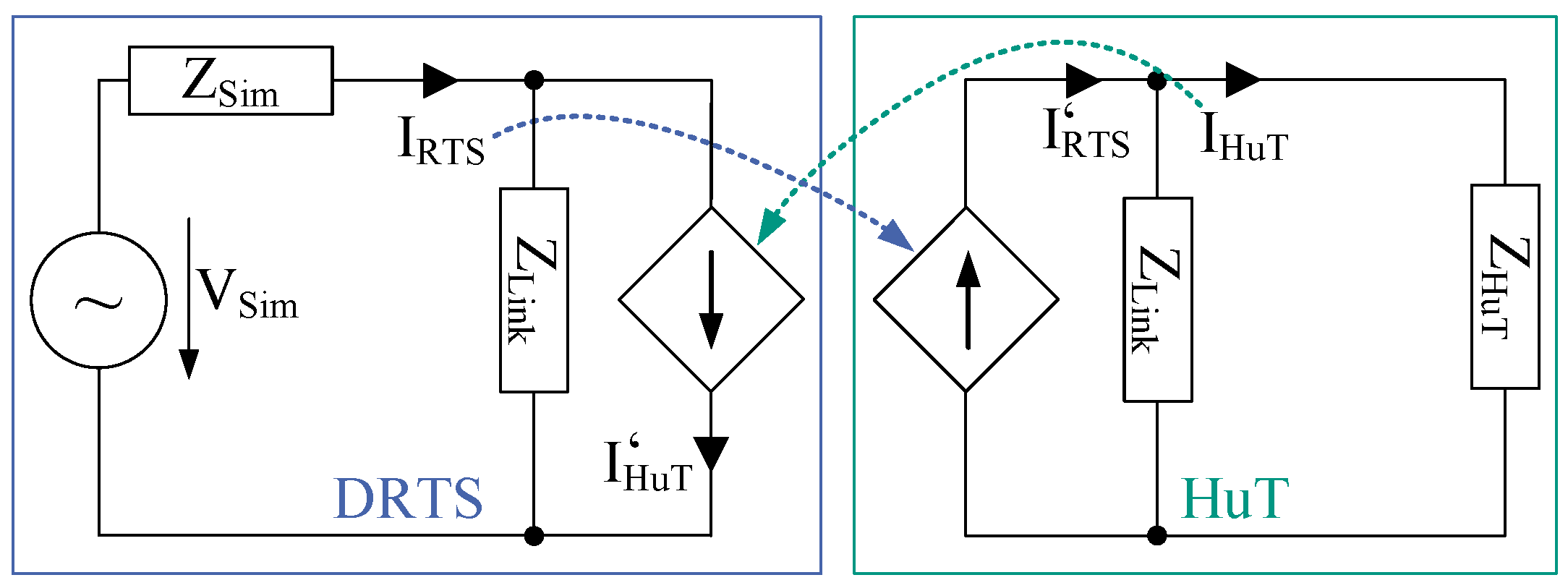
2.2.2. Current-Type PCD
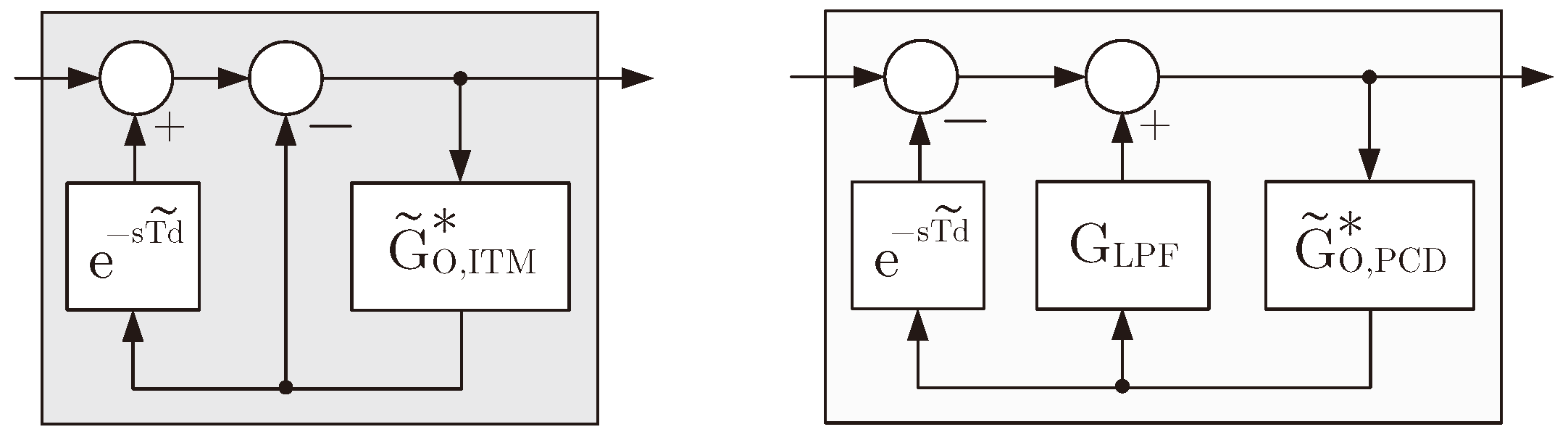
Figure 11 shows the equivalent circuit of the C-PCD. In this setting, the total current I RTS results from the voltage V Sim , the simulation impedance Z Sim , the simulated linking impedance Z Link , and the current I HuT from the last simulation step provided by the ideal current source. This setpoint is transmitted to the PA and set, which acts as a controlled current source. The current I RTS , the impedance Z HuT , and the linking impedance Z Link result in the total current I HuT , which is measured and fed back to the simulation using an ideal current source. After converting the current source into a voltage source on the simulation side, the control circuit in Figure 12 is obtained.
The impedances of both the simulation and the HuT are determined according to (14) and (15). The transfer functions of the C-PCD control loop are defined as follows:
G Gain = Z Link , G Sim = 1 Z Link + Z Sim
G HuT = Z Link Z HuT ( Z Link + Z HuT ) Z HuT
Whereas the C-PCD open loop transfer function G O , CPCD is calculated according to (16), the closed loop transfer function with positive feedback is defined as follows:
G C , CPCD = G Sim G PA G HuT 1 G O , CPCD
Figure 13 shows that a small linking impedance Z Link has a positive effect on stability. However, this reduces the accuracy. For an infinite Z Link , the control loop is theoretically unstable. In practice, parasitic effects such as measurement noise and numerical errors can also cause the control loop to become unstable for finite Z Link .

3. Smith Predictor

3.1. Compensated Voltage-Type ITM

To compensate system time delay, ref. [29] shows that an expression must be found that includes the estimated open loop transfer function without time delay G ˜ O and the estimated total time delay T ˜ d , which is summarized and shifted to the feedback path for simplified calculation. For V-ITM, the closed loop transfer function without time delay G C with SP is obtained as
G C , VITM = G PA 1 + G O , VITM e s T d + G ˜ O , VITM 1 e s T ˜ d
The equation for the SP can be transformed into a block diagram and integrated into the V-ITM, resulting in the control circuit depicted in Figure 14. If the estimated open loop transfer function, consisting of G PA , G Sim , and G HuT , is ideal, the closed loop equation can be simplified:
G C , VITM = G PA 1 + G ˜ O , VITM
In this SP approaches, the time delay is mathematically completely compensated, as the corresponding terms cancel each other out completely for an ideal SP model.
With the ideal estimated model, an impedance ratio of 1.2, and complete compensation of the time delay, the Nyquist curve of the open loop system is illustrated in Figure 15.
For different time delays and an impedance ratio of 1, this results in a GM rounded to 3.0, as shown in Table 1.

3.2. Compensated Current-Type ITM

As with the V-ITM, the estimation of the open loop transfer function and the time delay must be known for complete compensation. The following mathematical expression is derived for the closed loop:
G C , CITM = G PA G Sim 1 + G O , CITM e s T d + G ˜ O , CITM 1 e s T ˜ d
The block diagram of the SP is illustrated in the left diagram in Figure 16. The closed loop with ideal time delay compensation is defined as
G C , CITM = G PA G Sim 1 + G ˜ O , CITM
The rounded GM of the compensated open loop with SP is 3.0 for an impedance ratio of 1, as shown in Table 1.

3.3. Compensated Voltage-Type PCD

Theoretically, the control loop of the V-PCD can only become unstable if Z Link equals zero. A complete compensation of time delay eliminates the destructive interference and thus the resulting attenuation and phase shift. Due to the positive sum in the control loop, the SP transfer function must be derived in a modified way. The closed loop transfer function is defined as
G C , VPCD = G PA G Sim G HuT 1 G ˜ O , VPCD 1 e s T ˜ d G O , VPCD e s T d
In practice, effects such as measurement noise and numerical errors can lead to instability when Z Link is small. If the time delay is completely compensated by the SP, i.e., two sample times, the control loop can become unstable due to the effects mentioned or due to a minimal difference in the estimated model. This effect can be also observed when using the SP, since the SP does not significantly increase the GM, as can be concluded from Table 1. Therefore, the aim is to completely compensate the time delay, while maintaining sufficient attenuation at low Z Link in order to be able to keep the system stable. Therefore, a filtered SP is derived, which provides additional damping through an added first-order LPF. The block diagram of the filtered SP is illustrated in the right of Figure 16. The transfer function of the compensated closed loop is defined as follows:
G C , VPCD = G PA G Sim G HuT 1 G ˜ O , VPCD G LPF e s T ˜ d G O , VPCD e s T d
The integrated LPF reduces the dynamics and bandwidth depending on the cut-off frequency f c , LPF , which should therefore be selected as high as possible and be adapted to the setup. With an ideal estimated model, integrated LPF and complete time delay compensation, the following closed loop transfer function is achieved:
G C , VPCD = G PA G Sim G HuT 1 G ˜ O , VPCD G LPF
The significance and influence of the LPF for positive feedback IAs are explained using a clear example, which also makes practical design easier.
The following stability limit results for the Nyquist stability analysis with SP and integrated LPF:
| G ˜ O , VPCD G LPF + G ˜ O , VPCD e s T ˜ d G O , VPCD e s T d G O , VPCD | = 1
For this example, the estimated model of the SP assumed to be ideal:
G ˜ O , VPCD e s T ˜ d = G O , VPCD e s T d
If Z Link is also negligibly small, the following stability limit results:
| G ˜ O , VPCD G LPF | = | Z ˜ Sim Z ˜ HuT Z ˜ Sim Z ˜ HuT = 1 1 1 2 π f c , LPF s + 1 G LPF | = 1
The example shows that, in addition to the value of Z Link , stability can also be determined by selecting the LPF cut-off frequency. The idea behind the filtered SP is to compensate the negative characteristics of attenuation and phase shift caused by the time delay while increasing stability, whereby a smaller attenuation and phase shift caused by the LPF must be accepted. In addition to the theoretical design of the LPF cut-off frequency, it must be tuned in the PHIL setup, as parasitic effects are present in practice.

3.4. Compensated Current-Type PCD

The positive feedback of the control circuit means that the LPF also must be added in the C-PCD and the approach is equivalent to the approaches for the V-PCD. The closed loop transfer function is defined as follows:
G C , CPCD = G PA G Sim G HuT 1 G ˜ O , CPCD G LPF e s T ˜ d G O , CPCD e s T d
The following compensated closed loop transfer function results from the ideal estimated model, where the time delay is completely compensated:
G C , CPCD = G PA G Sim G HuT 1 G ˜ O , CPCD G LPF
In the right block diagram of Figure 16, the SP for C-PCD is depicted. The GM of the open loop with and without compensation by the SP is listed in Table 1.

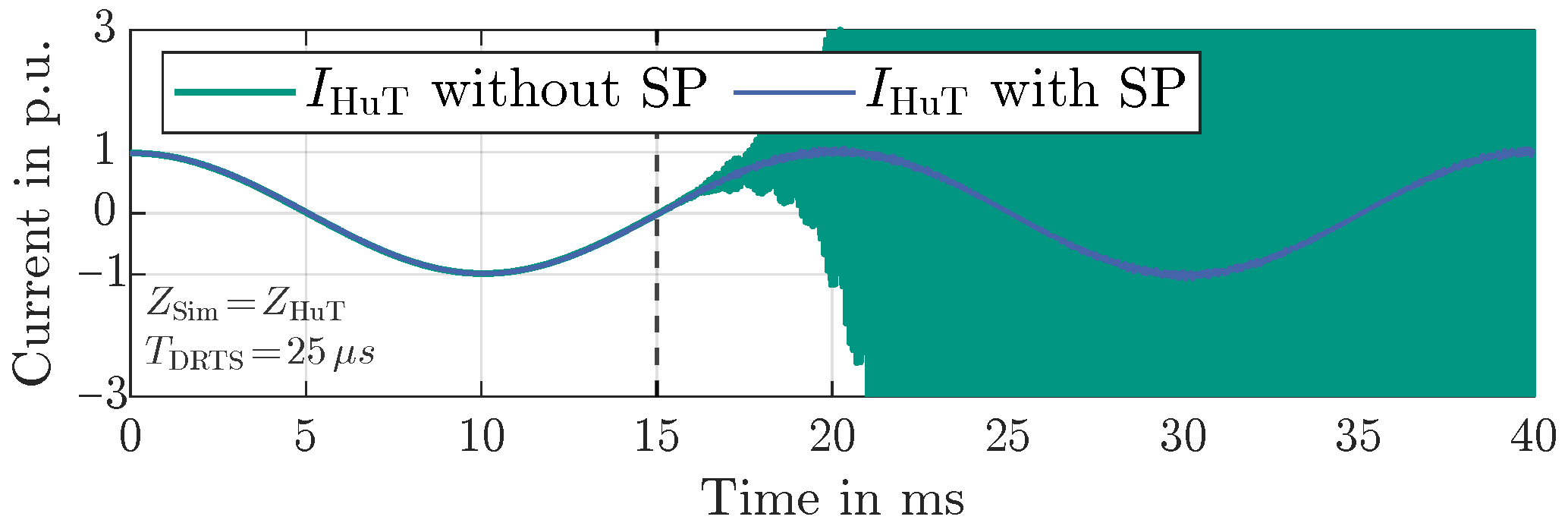
4. Simulation Results

To simulate the time delay compensation with the SP, MATLAB/Simulink is used. The transfer functions of the SP are discretized with the Tustin approximation and represented as a rational linear time-invariant (LTI) function in the z-domain. This allows changing the parameters of the SP in real-time and adjusting the estimated model at each discrete time step.

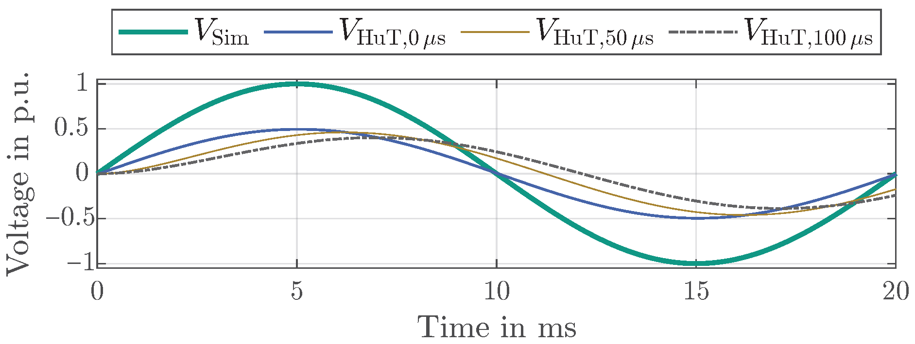
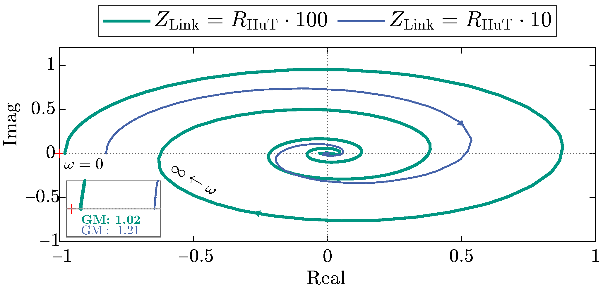
4.1. Negative Feedback: ITM

The behavior of the SP is analyzed in a simulation. Figure 17 illustrates the HuT current using the C-ITM, when a noise source is added at time t = 15 ms for a control loop operated at the stability limit. It can be observed that the control loop oscillates and becomes unstable without SP. In this state, the current oscillates at high frequencies with an increasing amplitude, ultimately saturating the entire figure. This unstable condition prevents safe PHIL operation and poses a risk to the HuT. With the SP, the control loop remains stable due to the established GM. The behavior with and without SP can be effectively compared for the V-ITM due to the negative feedback at the controller input and two other factors: Firstly, the system time delay is identical. Secondly, the V-ITM open loop transfer function is the same, except for a reciprocal impedance ratio, assuming the behavior of the PA is identical. For the V-ITM and inductive HuT, the current change is limited by the integrating behavior, which can have a positive effect on stability in practice. The results are shown in Table 1.

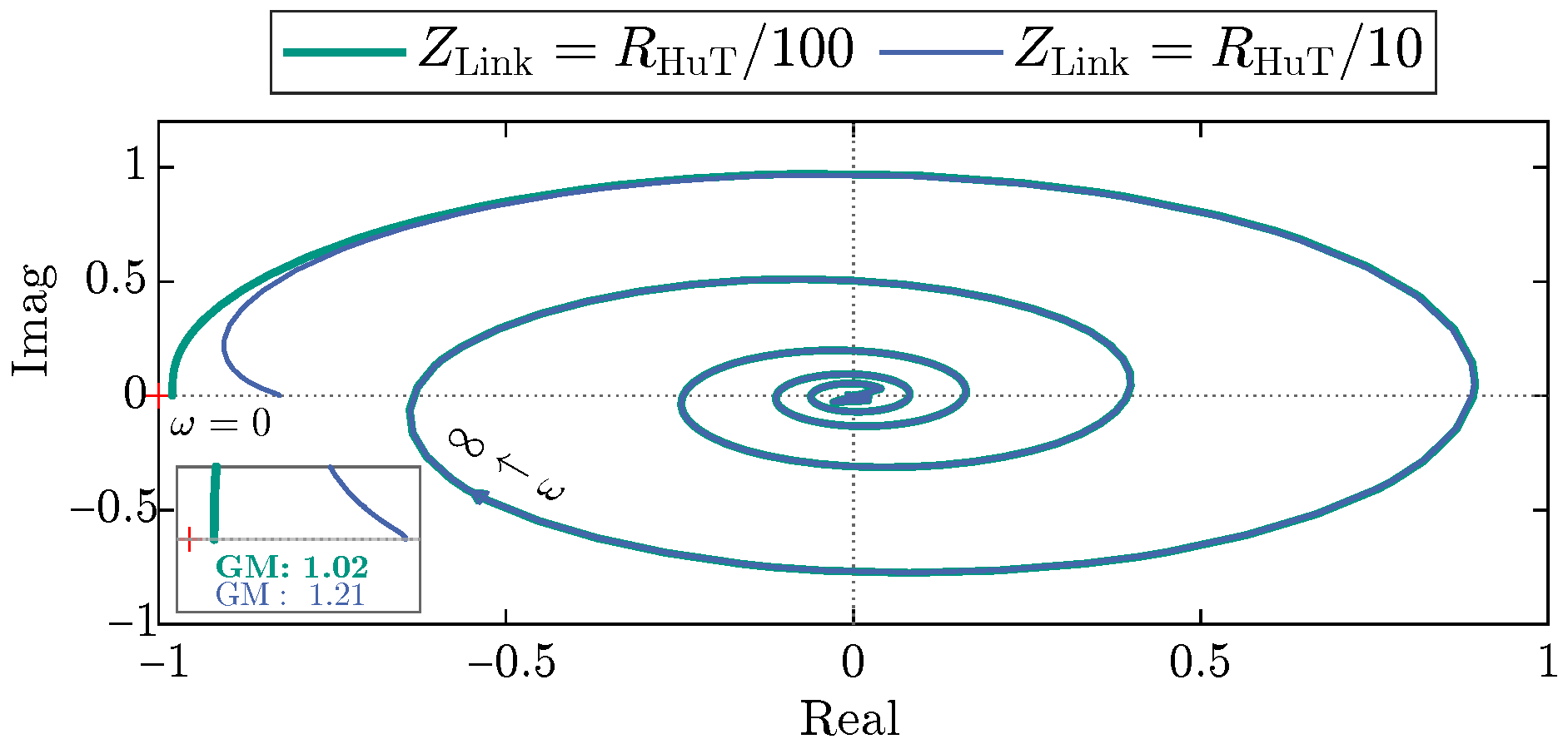
4.2. Positive Feedback: PCD

When the time delay is completely compensated by the SP, the result in the simulation for V-PCD as well as for C-PCD is an output signal without destructive interference, and thus without attenuation and phase shift, as shown in Figure 9 for V-PCD. Figure 18 shows a V-PCD control loop with damped SP, with f c , LPF = 6 kHz . At t = 15 ms , the filtered SP is deactivated. The results show that the phase shift increases by 9.53° and the attenuation of the output signal increases by 5% without filtered SP (5.2% and 9.44° for C-PCD).

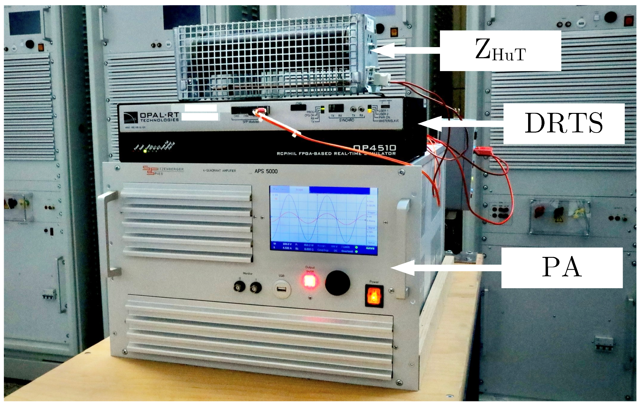
5. Experimental Results

To validate the functionality of the SP in the laboratory, the experimental circuit topology and hardware shown in Figure 19 and Figure 20 are used. The presented setup can be implemented independently of specific DRTS and PA manufacturers. For the PCD IAs, a coupling impedance Z Link is also required. The time delay of the continuous system is 4–6 µs, which is faster than the minimum used sample time T DRTS of 25 µs. Therefore, the maximum time delays according to (2) can be assumed for the SP.

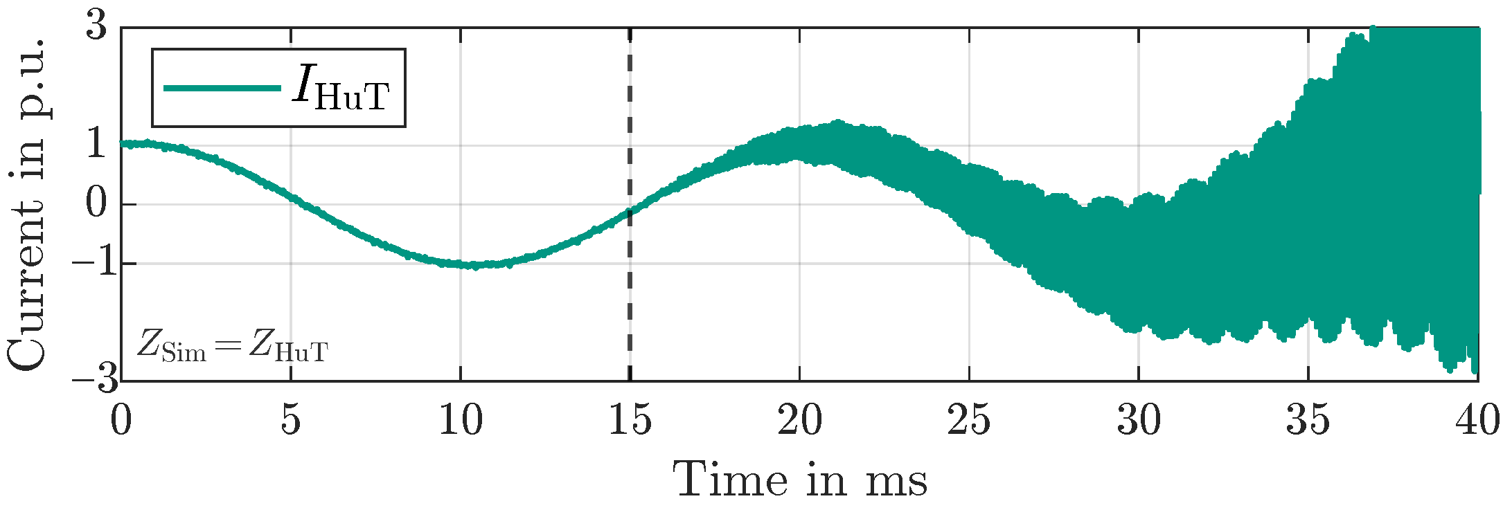
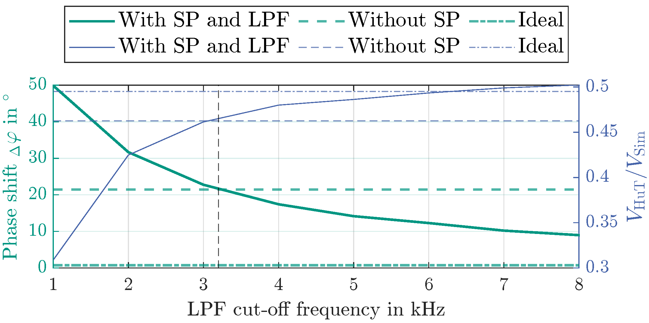
5.1. Negative Feedback: ITM

Figure 21 shows a C-ITM setup with SP, amplified by a disturbance factor of 1.1, where the HuT impedance is provided in Figure 20. At t = 15 ms , the SP is deactivated and the current oscillates. The system becomes unstable and has to be switched off. In this unstable state, the 50 Hz fundamental frequency is superimposed by high-frequency components.
To characterise the unstable state of the PHIL setup, the total harmonic distortion (THD) is calculated. A THD of 5 % is defined as an appropriate threshold for a stable condition, as already shown in [13,19]. Figure 22 shows the stability limit for a C-ITM setup. Without SP the unstable state occurs at a impedance ratio of 1.1. When the SP is activated, the maximum permissible impedance ratio increases to 2.96. Factors such as deviations in the estimated SP model, measurement inaccuracies and numerical errors can influence the result.
The estimated impedance of the HuT ( R ˜ HuT and L ˜ HuT ) is calculated in real-time by measuring the HuT voltage, the HuT current, and the phase shift between these 50 Hz values. Based on these measurements, the SP model can be dynamically adapted in real-time. This results in the GM remaining almost constant, as also shown in Figure 22. The slight increase in the THD with the impedance ratio is due to the resulting reduction in the amplitude of the HuT current and a constant noise signal. In theory, with an ideal SP model and no noise, the GM would be constant at a value rounded to 3.0. The measurement results and improvements of the V-ITM are well comparable with the C-ITM results.
In [31] a robust online method for characterizing the HuT’s frequency behavior for the SP model is presented, based on harmonic injection and discrete rational transfer function modeling. The frequency response is fitted using a differential evolution optimization algorithm, which offers resilience against measurement noise, incomplete datasets, and non-linearities in the z-domain. To demonstrate the effectiveness, a passive solar inverter and an R-L-C series connection are used as HuT. Additionally, the real-time capable technique for estimating the linearized 50 Hz impedance is demonstrated using a grid-feeding solar inverter.

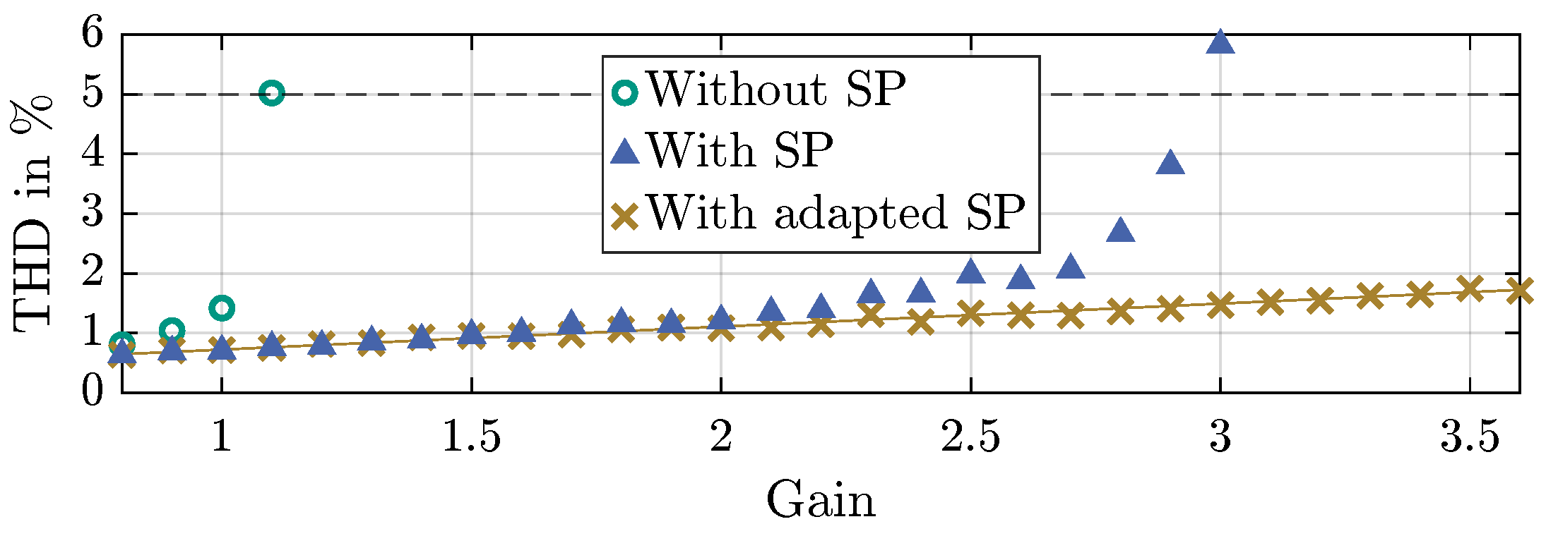
5.2. Positive Feedback: PCD

Figure 23 shows the influence of the SP on the phase shift and attenuation at different sample times. The influence of the filtered SP increases with increasing sample time, since destructive interference without SP also rises with increasing sample time. The cut-off frequency of the SP LPF is adjusted to the different sample times, varying between 4 kHz and 8 kHz , and causes a deviation from the ideal signal due to the damping behavior of the LPF. At a sample time of 100 µs and an LPF cut-off frequency of 4 kHz , the SP reduces the phase shift by 21.17° and the attenuation by 24.3%.
In practice, the linking impedance Z Link for V-PCD should be chosen as small as possible to minimize losses and to ensure high accuracy, while maintaining a stable system. Figure 24 illustrates the reduction in phase shift on the left y-axis with SP at a sample time of 50 µs and an LPF cut-off frequency of 6 kHz . The phase shift with SP is significantly reduced, especially at low ratios of Z Link to Z Sim . The right y-axis in Figure 24 illustrates the phase shift reduction with SP at different sample times and adjusted LPF cut-off frequencies. The reduction in phase shift is more pronounced at lower impedance ratios and increases with higher sample times. Note that the cutoff frequency must be selected based on the sample time and the specific setup. Therefore, in addition to the theoretical design, practical adjustments are made during the experimental setup, starting with a lower cut-off frequency and considering the observed system behavior and prevailing noise level.
Figure 25 demonstrates the impact of cut-off frequency on phase shift and attenuation with a fixed sample time of 50 µs. With a cut-off frequency of 3.2 kHz , the SP significantly reduces both phase shift and attenuation compared to a setup without SP. To minimize phase shift and attenuation with SP, a high cut-off frequency must be chosen. However, it should still be small enough to maintain sufficient GM and ensure stable system operation. A cut-off frequency of 6 kHz works well in this example. Beyond 6 kHz , instability occurs, evident by the increase in output voltage amplitude beyond the theoretical maximum. The measurement results and enhancements of the C-PCD are highly comparable to those of the V-PCD.

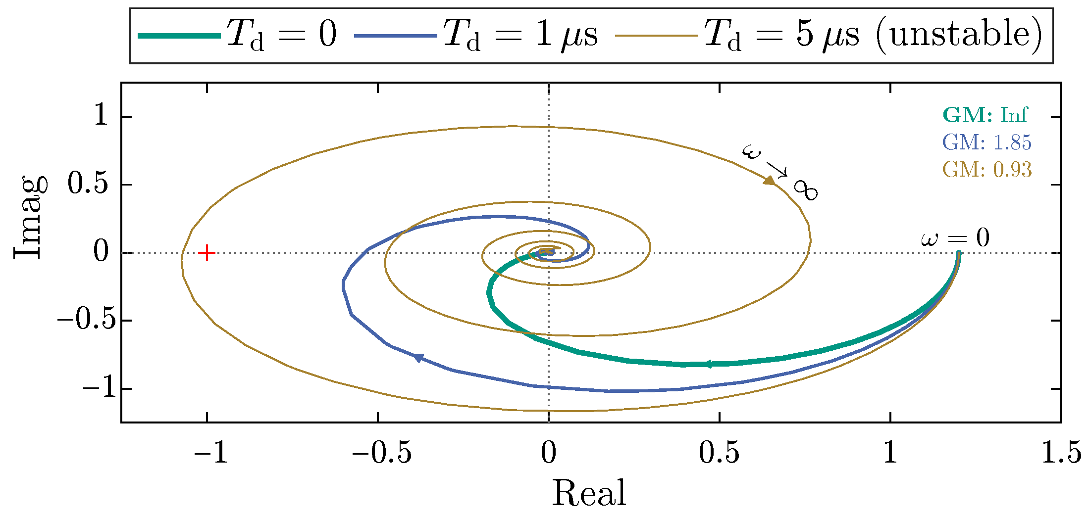
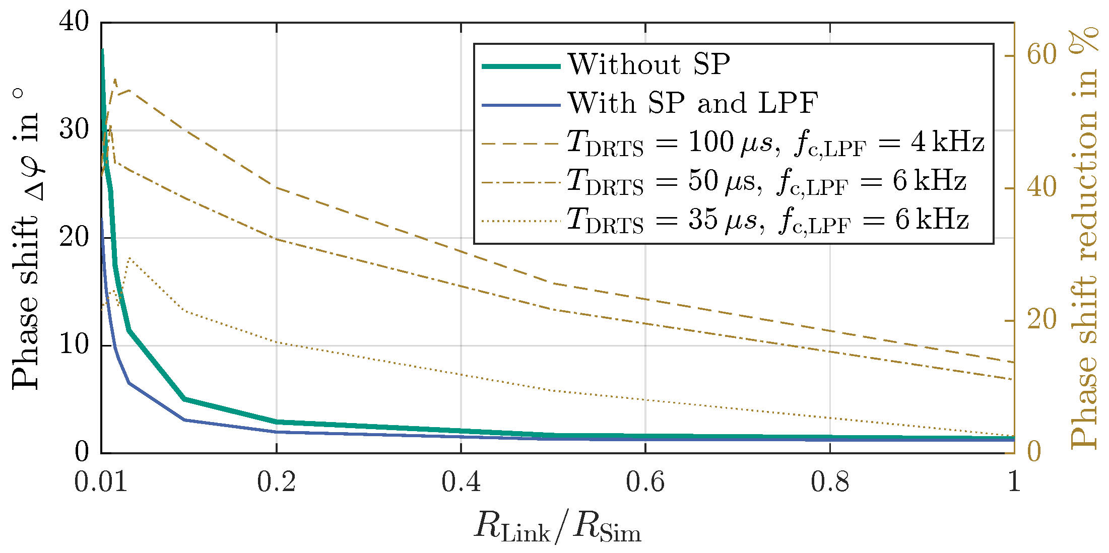
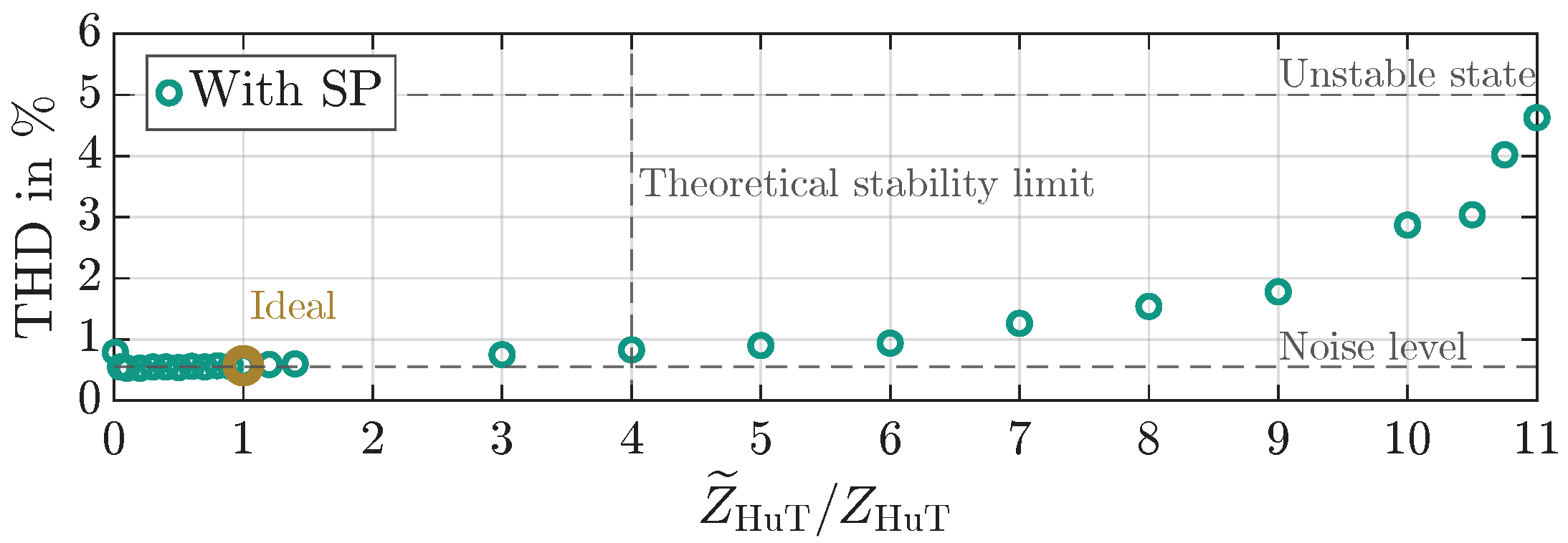
5.3. Influence of SP Model Deviation

In practical SP approaches, a perfect SP model in the DRTS and a constant HuT impedance are not possible. There are several reasons for this: Firstly, the precise real-time determination of the HuT impedance is infeasible, as it is subject to variations depending on the operating point and additional factors such as temperature. Secondly, in cases of nonlinear HuT behavior, the impedance may change abruptly. Thirdly, the DRTS approximates the differential equations in discrete increments at defined time steps, so all transfer functions used in the simulation are Tustin-discretized and implemented as rational LTI transfer functions. These differences between the discrete SP model and real impedances cause additional deviations. If all these points are considered, stable PHIL operation should be possible within certain limits even if the estimated HuT impedance of the SP is not ideal or if the real HuT impedance changes abruptly.
To investigate the influence of an inaccurate SP model on system stability, the estimated HuT impedance Z ˜ HuT of the SP model is varied in the first scenario, while the actual HuT impedance Z HuT remains constant. The limits of modeling inaccuracies that still allow stable operation are illustrated in Figure 26. The unstable V-ITM IA configuration with Z Sim = 2 · Z HuT is stabilized by the SP. However, if the ratio of inaccuracy exceeds a value of 11 in the experiment, the system begins to run unstably ( THD > 5 % ). Stable operation is preserved for ratios down to 0.01. In theory, the V-ITM IA open loop transfer function with SP and without PA, derived from (21), reaches its Nyquist stability limit at a ratio of four:
with Z Sim = 2 · Z HuT and Z ˜ Sim = 2 · Z ˜ HuT
2 Z HuT Z HuT e s T d + 2 Z ˜ HuT 4 Z ˜ HuT 2 Z ˜ HuT 4 Z ˜ HuT e s T ˜ d = 2 0.5 e s T d + 0.5 < 1
In Figure 26, an increase in THD can already be observed here and the PA further increases the stability limit. Stability improves when the ratio between the estimated and actual HuT impedance is smaller than one. However, the deviations cause a slight deterioration in accuracy.
In the second scenario, the effect on stability is now examined when the real HuT impedance Z HuT changes, while Z ˜ HuT remains constant. In this case, the V-ITM setup is also operated under unstable conditions, which means Z Sim = 2 · Z HuT and Z ˜ Sim = 2 · Z ˜ HuT . The following stability condition results in a minimum factor X that constrains the maximum variation of the real Z HuT and must not be undershot. In this example, this leads to X = 0.4 . If this threshold is not undershot, the system remains stable with a constant SP model, even in the event of a sudden impedance change, as occurs during a low-voltage ride through or with non-linear loads.
2 Z HuT X Z HuT e s T d + 2 Z ˜ HuT Z ˜ HuT 2 Z ˜ HuT Z ˜ HuT e s T ˜ d = 2 X 2 e s T d + 2 < 1

6. Conclusions and Outlook

This article derives the transfer functions of the SP for V-ITM, C-ITM, V-PCD, and C-PCD IAs and integrates them into PHIL simulations and experiments. The SP compensates system time delay in all settings. The V-ITM and C-ITM with negative feedback benefit from the SP’s ability to improve stability and accuracy. The GM could be increased from approximately one to three. Real-time HuT impedance calculation and dynamic SP adaptation enhance stability and maintain a nearly constant GM of approximately three. Stable PHIL operation is also possible with a non-ideal SP model or if the HuT impedance changes abruptly, as long as the deviation between the estimated and actual HuT impedance remains within certain limits. In the V-PCD and C-PCD IAs, positive feedback causes destructive interference, increasing phase shift and attenuation with time delay. A novel damped SP with an integrated LPF compensates time delay, reducing phase shift and attenuation. This filtered SP enables stable, accurate operation for the V-PCD and C-PCD IAs. The filtered SP enabled a reduction in phase shift by 21.17° and a decrease in attenuation by 24.3% for the V-PCD IAs. Compensating time delay with SP expands the use of cheaper DRTS systems with larger sample times by improving stability and accuracy.
Future research will focus on applying the SP approach to further grid use cases, with the objective of analyzing the dynamic behavior of real HuT in compensated PHIL environments.

Author Contributions

Conceptualization, L.B. and J.M.; methodology, L.B. and J.M.; software, L.B. and J.M.; validation, L.B., J.M., M.S. and T.L.; writing—original draft preparation, L.B.; writing—review and editing, L.B., J.M., M.S. and T.L.; supervision, M.S. and T.L. All authors have read and agreed to the published version of the manuscript.

Funding

This work was supported by the Helmholtz Association of German Research Centres (HGF) within the framework of the Program-Oriented Funding POF IV in the program Energy Systems Design (ESD, project number 37.12.02).

Data Availability Statement

The data are not publicly available beyond what is presented in the paper, as not all involved authors have agreed to its publication. For further information regarding the presented data and other inquiries, please contact the corresponding author.

Conflicts of Interest

The authors declare no conflicts of interest.

Abbreviations

The following abbreviations are used in this manuscript:
C-current-type
DRTSdigital real-time simulator
EMTelectromagnetic transient
GMgain margin
HuThardware under test
IAinterface algorithm
ITMideal transformer method
LPFlow-pass filter
OLoptical link
PApower amplifier
PCDpartial circuit duplication
PHILpower hardware-in-the-loop
SPSmith predictor
TLMtransmission line model
V-voltage-type

References

  1. Chang, H.; Vanfretti, L. A power hardware-in-the-loop smart inverter testing facility. In Proceedings of the 2024 9th International Conference on Smart and Sustainable Technologies (SpliTech), Bol and Split, Croatia, 25–28 June 2024; pp. 1–6. [Google Scholar]
  2. Pokharel, M.; Ho, C.N.M. Stability analysis of power hardware-in-the-loop architecture with solar inverter. IEEE Trans. Ind. Electron. 2021, 68, 4309–4319. [Google Scholar] [CrossRef]
  3. Langston, J.; Schoder, K.; Steurer, M.; Faruque, O.; Hauer, J.; Bogdan, F.; Bravo, R.; Mather, B.; Katiraei, F. Power hardware-in-the-loop testing of a 500 kW photovoltaic array inverter. In Proceedings of the 38th Annual Conference on IEEE Industrial Electronics Society, Montreal, QC, Canada, 25–28 October 2012; pp. 4797–4802. [Google Scholar]
  4. Kim, J.-G.; Kim, S.-K.; Park, M.; Yu, I.-K. Hardware-in-the-loop simulation for superconducting DC power transmission system. IEEE Trans. Appl. Supercond. 2015, 25, 5402404. [Google Scholar] [CrossRef]
  5. Watanabe, K.; Langston, J.; Hauer, J.; Coleman, M.; Stanovich, M.; Izumida, Y.; Steurer, M. Power hardware-in-the-loop simulation to verify protection coordination for DC microgrid. In Proceedings of the 2023 IEEE Applied Power Electronics Conference and Exposition (APEC), Orlando, FL, USA, 19–23 March 2023; pp. 2646–2653. [Google Scholar]
  6. Gómez-Luna, E.; Candelo-Becerra, J.E.; Vasquez, J.C. A new digital twins-based overcurrent protection scheme for distributed energy resources integrated distribution networks. Energies 2023, 16, 5545. [Google Scholar] [CrossRef]
  7. Karrari, S.; Noe, M.; Geisbuesch, J. High-speed flywheel energy storage system (FESS) for voltage and frequency support in low voltage distribution networks. In Proceedings of the 2018 IEEE 3rd International Conference on Intelligent Energy and Power Systems (IEPS), Kharkiv, Ukraine, 10–14 September 2018; pp. 176–182. [Google Scholar]
  8. Debouza, M.; Al-Durra, A.; El-Fouly, T.H.M.; Zeineldin, H.H. Establishing realistic testbeds for DC microgrids studies validation: Needs and challenges. In Proceedings of the 2020 IEEE Industry Applications Society Annual Meeting, Detroit, MI, USA, 10–16 October 2020; pp. 1–8. [Google Scholar]
  9. Singh, S.K.; Padhy, B.P.; Chakrabarti, S.; Singh, S.N.; Kolwalkar, A.; Kelapure, S.M. Development of dynamic test cases in OPAL-RT real-time power system simulator. In Proceedings of the 2014 Eighteenth National Power Systems Conference (NPSC), Guwahati, India, 18–20 December 2014; pp. 1–6. [Google Scholar]
  10. Braun, L.; Kist, S.; Eser, D.; Suriyah, M.; Leibfried, T. Stability improvement of a dynamic low-voltage power hardware-in-the-loop environment. In Proceedings of the Conference Sustainable Energy Supply Energy Storage Systems (NEIS), Hamburg, Germany, 16–17 September 2024. [Google Scholar]
  11. Ihrens, J.; Möws, S.; Wilkening, L.; Kern, T.A.; Becker, C. The impact of time delays for power hardware-in-the-loop investigations. Energies 2021, 14, 3154. [Google Scholar] [CrossRef]
  12. Lauss, G.F.; Faruque, M.O.; Schoder, K.; Dufour, C.; Viehweider, A.; Langston, J. Characteristics and design of power hardware-in-the-loop simulations for electrical power systems. IEEE Trans. Ind. Electron. 2016, 63, 406–417. [Google Scholar] [CrossRef]
  13. Braun, L.; Lutz, L.G.; Suriyah, M.; Leibfried, T. Establishing a PLC-based power hardware-in-the-loop setup for power grid applications. In Proceedings of the 2024 9th IEEE Workshop on the Electronic Grid (eGRID), Santa Fe, NM, USA, 19–21 November 2024; pp. 1–5. [Google Scholar]
  14. Lu, B.; Wu, X.; Figueroa, H.; Monti, A. A low-cost real-time hardware-in-the-loop testing approach of power electronics controls. IEEE Trans. Ind. Electron. 2007, 54, 919–931. [Google Scholar] [CrossRef]
  15. Resch, S.; Friedrich, J.; Wagner, T.; Mehlmann, G.; Luther, M. Stability analysis of power hardware-in-the-loop simulations for grid applications. Electronics 2022, 11, 7. [Google Scholar] [CrossRef]
  16. Ashrafidehkordi, F.; Kottonau, D.; Carne, G.D. Multi-rate discrete domain modeling of power hardware-in-the-loop setups. IEEE Open Power Electron. 2023, 4, 539–548. [Google Scholar] [CrossRef]
  17. Li, F.; Huang, Y.; Wu, F.; Zhang, X.; Zhao, W. Power-hardware-in-the-loop stability analysis of inverter. In Proceedings of the 2019 22nd International Conference on Electrical Machines and Systems (ICEMS), Harbin, China, 11–14 August 2019; pp. 1–5. [Google Scholar]
  18. Hong, M.; Horie, S.; Miura, Y.; Ise, T.; Dufour, C. A method to stabilize a power hardware-in-the-loop simulation of inductor coupled systems. In Proceedings of the International Conference on Power System Transients (IPST), Kyoto, Japan, 2–6 June 2009; pp. 1–7. [Google Scholar]
  19. Braun, L.; Kist, S.; Suriyah, M.; Leibfried, T. Stability analysis and real-time optimization of a power hardware-in-the-loop setup. In Proceedings of the 2024 59th International Universities Power Engineering Conference (UPEC), Cardiff, UK, 2–6 September 2024. [Google Scholar]
  20. Wang, J.; Lundstrom, B.; Mendoza, I.; Pratt, A. Systematic characterization of power hardware-in-the-loop evaluation platform stability. In Proceedings of the 2019 IEEE Energy Conversion Congress and Exposition (ECCE), Baltimore, MD, USA, 29 September–3 October 2019; pp. 1068–1075. [Google Scholar]
  21. Ren, W.; Steurer, M.; Baldwin, T.L. Improve the stability and the accuracy of power hardware-in-the-loop simulation by selecting appropriate interface algorithms. In Proceedings of the 2007 IEEE/IAS Industrial & Commercial Power Systems Technical Conference, Edmonton, AB, Canada, 6–11 May 2007; pp. 1–7. [Google Scholar]
  22. Lauss, G.; Lehfuß, F.; Viehweider, A.; Strasser, T. Power hardware-in-the-loop simulation with feedback current filtering for electric systems. In Proceedings of the 37th Annual Conference of the IEEE Industrial Electronics Society, Melbourne, VIC, Australia, 7–10 November 2011; pp. 3725–3730. [Google Scholar]
  23. Dmitriev-Zdorov, V.B. Generalized coupling as a way to improve the convergence in relaxation-based solvers. In Proceedings of the EURO-DAC ’96. European Design Automation Conference with EURO-VHDL ’96 and Exhibition, Geneva, Switzerland, 16–20 September 1996; pp. 15–20. [Google Scholar]
  24. Edrington, C.S.; Steurer, M.; Langston, J.; El-Mezyani, T.; Schoder, K. Role of power hardware in the loop in modeling and simulation for experimentation in power and energy systems. Proc. IEEE 2015, 103, 2401–2409. [Google Scholar] [CrossRef]
  25. Brandl, R. Operational range of several interface algorithms for different power hardware-in-the-loop setups. Energies 2017, 10, 1946. [Google Scholar] [CrossRef]
  26. Loku, F.; Osterkamp, L.; Düllmann, P.; Klein, C.; Maimer, M.; Bergwinkl, T. Utilization of the Impedance-based Stability Criterion for Stability Assessment of PHiL Interface Algorithms. In Proceedings of the 2022 IEEE 13th International Symposium on Power Electronics for Distributed Generation Systems (PEDG), Kiel, Germany, 26–29 June 2022; pp. 1–7. [Google Scholar]
  27. Benedetto, G.; Mazza, A.; Pons, E.; Bompard, E. Key Stability Issues in a Power Hardware-In-the-Loop Experiment: Let’s Make it Converge. In Proceedings of the 2023 IEEE International Conference on Environment and Electrical Engineering and 2023 IEEE Industrial and Commercial Power Systems Europe (EEEIC/I&CPS Europe), Madrid, Spain, 6–9 June 2023; pp. 1–6. [Google Scholar]
  28. Schwendemann, R.; Stefanski, L.; Hiller, M. Comparison of different interface algorithms for a highly dynamic grid emulator based on a series hybrid converter. In Proceedings of the 2022 IEEE 23rd Workshop on Control and Modeling for Power Electronics (COMPEL), Tel Aviv, Israel, 20–23 June 2022; pp. 1–8. [Google Scholar]
  29. Feng, Z.; Peña-Alzola, R.; Syed, M.H.; Norman, P.J.; Burt, G.M. Adaptive Smith predictor for enhanced stability of power hardware-in-the-loop setups. IEEE Trans. Ind. Electron. 2023, 70, 10204–10214. [Google Scholar] [CrossRef]
  30. Pokharel, M.; Ho, C.N.M. Development of interface model and design of compensator to overcome delay response in a PHIL setup for evaluating a grid-connected power electronic DUT. IEEE Trans. Ind. Appl. 2022, 58, 4109–4121. [Google Scholar] [CrossRef]
  31. Braun, L.; Suriyah, M.; Leibfried, T. Online Impedance Identification and Transfer Function Modeling in PHIL Applications. In Proceedings of the 2025 IEEE International Conference on Environment and Electrical Engineering and 2025 IEEE Industrial and Commercial Power Systems Europe (EEEIC/I&CPS Europe), Chania, Greece, 15–18 July 2025. [Google Scholar]
Figure 1. Comparison between ITM and PCD IA - the linking impedance effects the trade-off between accuracy, bandwidth, dynamics, stability, and scope.
Energies 18 03773 g001
Figure 2. Equivalent circuit of V-ITM IA.
Energies 18 03773 g002
Figure 3. Block diagram of V-ITM IA.
Energies 18 03773 g003
Figure 4. Influence of system time delay on GM: V-ITM ( Z Sim = 1.2 · Z HuT , see (3) and (4)) or C-ITM ( Z HuT = 1.2 · Z Sim , see (8) and (9)).
Energies 18 03773 g004
Figure 5. Equivalent circuit of C-ITM IA.
Energies 18 03773 g005
Figure 6. Block diagram of C-ITM IA.
Energies 18 03773 g006
Figure 7. Equivalent circuit of V-PCD IA.
Energies 18 03773 g007
Figure 8. Block diagram of V-PCD IA.
Energies 18 03773 g008
Figure 9. Influence of the time delay on the attenuation and the phase shift of the output signal in the V-PCD due to destructive interference with Z Sim = Z HuT and Z Link = R Sim / 50 ; see (14) and (15).
Energies 18 03773 g009
Figure 10. Influence of the linking impedance on the GM of the V-PCD, at T d = 5 µs and Z HuT = Z Sim ; see (14) and (15).
Energies 18 03773 g010
Figure 11. Equivalent circuit of C-PCD IA.
Energies 18 03773 g011
Figure 12. Block diagram of C-PCD IA.
Energies 18 03773 g012
Figure 13. Influence of the linking impedance on the GM of the C-PCD, at T d = 5 µs and Z HuT = Z Sim ; see (14) and (15).
Energies 18 03773 g013
Figure 14. Block diagram of compensated V-ITM IA.
Energies 18 03773 g014
Figure 15. Time delay compensation by the SP at the V-ITM increases GM, with Z Sim = 1.2 · Z HuT ; see (3) and (4) (cf. Figure 4).
Energies 18 03773 g015
Figure 16. Block diagram of SP for ITM (left) and PCD (right).
Energies 18 03773 g016
Figure 17. Simulation: C-ITM with activated disturbance factor = 1.1 at t = 15 ms ; see (8) and (9).
Energies 18 03773 g017
Figure 18. Simulation: Increase in phase shift and attenuation after deactivating compensated SP ( f c , LPF = 6 kHz ) at t = 15 ms at V-PCD; see (14) and (15).
Energies 18 03773 g018
Figure 19. Photograph of the experimental PHIL laboratory setup.
Energies 18 03773 g019
Figure 20. Experimental circuit topology ( G PA , compare (5)).
Energies 18 03773 g020
Figure 21. Experiment: Unstable C-ITM with disturbance factor = 1.1 and deactivated SP at t = 15 ms ( T DRTS = 25 µs); see (8) and (9) (cf. Figure 17).
Energies 18 03773 g021
Figure 22. Experiment: C-ITM stability limits with increasing impedance ratio ( T DRTS = 25 µs), which means Z HuT = Gain · Z Sim (see (8) and (9)).
Energies 18 03773 g022
Figure 23. Experiment: Attenuation and phase shift between V HuT and V Sim at V-PCD ( Z Link = R Sim / 50 and Z Sim = Z HuT ); see (14) and (15).
Energies 18 03773 g023
Figure 24. Experiment: V-PCD phase shift between V HuT and V Sim (left y-axis) and phase shift reduction for different time delays with SP (right y-axis) ( Z Sim = Z HuT , see (14) and (15)).
Energies 18 03773 g024
Figure 25. Experiment: V-PCD phase shift and attenuation between V HuT and V Sim ( T DRTS = 50 µs) at different LPF cut-off frequencies, with Z Sim = Z HuT and Z Link = R Sim / 50 ; see (14) and (15).
Energies 18 03773 g025
Figure 26. Experiment: Influence of the deviation between estimated SP HuT impedance and real HuT impedance at V-ITM ( T DRTS = 25 µs), with Z Sim = 2 · Z HuT ; see (3) and (4).
Energies 18 03773 g026
Table 1. Theoretical GMs at different time delays for ITM and PCD with and without SP. For PCD an LPF is added in the SP (marked as *).
Z Sim = Z HuT = s 620 μ H + 22.18 Ω | Z Link , VPCD = R Sim / 50 | Z Link , CPCD = 50 R Sim    f c , LPF = 6 kHz
T d in µsV-ITM/C-ITMV-ITM/C-ITM with SPV-PCDV-PCD with SP ∗C-PCDC-PCD with SP ∗
51.11992.96921.04041.04041.04041.0404
501.00182.99941.01051.04041.05211.0404
701.00092.99971.00951.04041.04651.0404
1001.00052.99991.01061.04041.04351.0404
Disclaimer/Publisher’s Note: The statements, opinions and data contained in all publications are solely those of the individual author(s) and contributor(s) and not of MDPI and/or the editor(s). MDPI and/or the editor(s) disclaim responsibility for any injury to people or property resulting from any ideas, methods, instructions or products referred to in the content.

