Article

Topology Analysis and Modeling Comparison of SI-SIMO Boost Converter Used in Multiple Output Applications

1
College of Electrical Engineering, Qingdao University, Qingdao 266071, China
2
College of Electrical Engineering, Sichuan University, Chengdu 610065, China
*
Authors to whom correspondence should be addressed.
Energies 2025, 18(13), 3585; https://doi.org/10.3390/en18133585
Submission received: 28 May 2025 / Revised: 20 June 2025 / Accepted: 25 June 2025 / Published: 7 July 2025

Abstract

This paper presents the analysis and modeling of a single-input, single-inductor, multiple-output (SI-SIMO) boost converter to address limitations of conventional SISO converters in distributed power supply applications. Based on switching-state analysis, a sequential PWM modulation strategy is proposed to achieve independent voltage regulation across multiple outputs using a single inductor. An average circuit model is developed considering steady-state characteristics. Inductor conduction mode boundaries and the critical inductor value are derived. A complete modeling process is introduced, transitioning from nonlinear dynamics to small-signal approximation at the steady-state operating point. PSIM and MATLAB Simulink experiment results validate the proposed control method and confirm the theoretical analysis under various operating conditions.

1. Introduction

Escalating global energy demands have positioned electricity as the primary energy medium due to its efficiency and sustainability, driving the need for multiport power converters to optimize energy distribution. While advancements in converter topologies address heterogeneous source–load integration, technical limitations persist. In PV systems, DC-DC converters boost solar panel outputs to grid-compatible levels. Recent designs like switched-inductor–capacitor modules enhance voltage gain but increase component complexity and cost [1,2]. Alternative dual-inductor configurations with capacitors achieve comparable gains without extreme duty cycles [3,4] yet suffer from 10 kHz switching losses and ESR-related inefficiencies, capping maximum efficiency at 92–93%. These challenges highlight critical trade-offs between performance gains and operational reliability in converter design.
Residential AC-DC conversion requires efficient grid-to-appliance interfaces. While [5] proposes a zero-current switching (ZCS) current-fed full-bridge converter with 15% lower conduction losses via resonant commutation, it suffers from 600 V+ voltage stress on primary devices. In paper [6], the author mitigates this with an active lossless clamp (ALC) (450 V spikes, <5% THD), yet transient load shifts induce DC bus ripples (~2.5%) due to limited control bandwidth. Collectively, [1,2,3,4,5,6] reveal systemic trade-offs: DC-DC designs balance voltage gains vs. parasitic losses, while AC-DC systems face soft-switching benefits versus resonance challenges. Future efforts must integrate modular topologies, wide-bandgap devices, and adaptive controls to address efficiency, stress, and dynamic response limitations.
Although existing multiport power converters have many limitations, they still play a significant role in modern society and provide substantial convenience to users. Hence, advanced study on multiple-port DC-DC converters is critical in modern intelligent energy systems and consuming electronic devices [7].
In recent research focused on multiport power converters, related literature studies are primarily categorized into two groups: isolated and non-isolated types. Owing to the absence of isolation transformers, non-isolated converters exhibit advantages such as simplified design, reduced weight, lower cost, and more compact dimensions. Non-isolated converters employ shared grounding between input and output ports, offering simplified designs and reduced component counts. Common topologies include bidirectional buck-boost, Cuk/SEPIC/ZETA, interleaved, switched capacitor, and cascaded converters. For instance, bidirectional buck-boost converters regulate power flow through duty cycle modulation, operating in buck mode (when input voltage exceeds output) or boost mode (vice versa). Similarly, interleaved converters reduce current ripples by splitting current across multiple phases, enhancing power density [8]. However, non-isolated topologies face inherent limitations: the absence of galvanic isolation increases vulnerability to fault propagation between ports, and high-voltage/current stresses on switches degrade efficiency in high-power applications. Additionally, coupled inductors or cascaded designs introduce control complexity and component redundancy, limiting scalability [9].
Isolated converters, in contrast, utilize high-frequency transformers to decouple input and output ports, ensuring safety and electromagnetic isolation. Key topologies include flyback, dual active bridge (DAB), and multi-winding transformer-based converters. Flyback converters, functioning as isolated buck-boost converters, are constrained to low-power applications (≤150 W) due to high voltage stress on switching devices and the necessity for bulky transformer cores [10]. In contrast, DAB converters excel in high-power scenarios (>2 kW) by leveraging phase-shift control between dual active bridges to regulate bidirectional power flow [11]. To achieve high-power density and soft-switching capabilities, their control complexity escalates with circulating currents, leakage inductance effects, and the need for precise phase-shift modulation. Multi-winding transformer-based converters further integrate multiple ports but struggle with independent output regulation due to magnetic coupling between windings, necessitating advanced decoupling algorithms to mitigate cross-regulation [12,13].
Comparative analyses reveal trade-offs between these categories. Non-isolated converters exhibit higher efficiency and lower costs for low-power applications but lack fault tolerance and voltage flexibility [14]. Isolated converters, though bulkier and costlier, provide superior voltage scalability and safety for grid-connected systems [15]. Challenges persist in both domains: non-isolated designs grapple with efficiency degradation at high duty cycles, while isolated variants face switching loss minimization and transformer optimization hurdles [16]. Innovations such as soft-switching techniques (ZVS/ZCS) and modular multiport architectures are being explored to address these limitations, aiming to enhance power density, efficiency, and controllability in hybrid energy systems [17].
DC-DC converters play a pivotal role in renewable energy integration and power management systems [18], with diverse topologies addressing specific requirements while exhibiting inherent limitations. Non-isolated topologies such as SEPIC, Cuk, and Zeta converters offer voltage gain flexibility but face challenges including component complexity, high voltage stress on switches, and efficiency trade-offs. For instance, SEPIC converters require multiple inductors and capacitors, increasing system footprint and cost, while Cuk converters exhibit polarity inversion and elevated switching losses. Coupled-inductor-based designs like Z-source converters achieve moderate voltage gain with reduced duty cycle dependence [19], yet they suffer from leakage inductance effects and limited scalability for multiport applications. Multi-phase interleaved converters demonstrate reduced input current ripple, but their high device count (e.g., 27 components in six-phase configurations) and complex control algorithms hinder cost-effectiveness. Recent advancements in three-port converters enable flexible energy exchange in microgrids, though their reliance on multi-switch architectures introduces control coupling challenges and switching loss accumulation [20]. While voltage multiplier cells and switched-capacitor techniques achieve ultra-high gains (>10×), they often require extensive passive components and suffer from capacitor voltage imbalance issues. Boost-derived topologies remain prevalent in photovoltaic systems due to their structural simplicity, yet conventional implementations struggle with extreme duty cycle requirements (>0.75) that exacerbate switching losses and electromagnetic interference [21]. These limitations highlight the need for innovative single-inductor architectures that balance voltage gain, component count, and control simplicity—a gap addressed by advanced boost-based designs through topological optimization and multi-output integration. Therefore, a multiport boost converter with a single inductor and fully independently controllable operation is demanded in distributed power storage and consumption systems.
In recent advancements in DC-DC converter technology, the Single-Inductor Multi-Output (SIMO) boost converter has emerged as an optimal topology for applications requiring multiple regulated voltage outputs from a single power source [22]. This architecture employs time-multiplexed switching control to power multiple-output channels through a shared magnetic component (single inductor), demonstrating significant advantages in component minimization and system miniaturization [23]. The unified magnetic structure fundamentally simplifies power stage design: by consolidating energy storage and distribution into a single inductive element, it eliminates redundant magnetic components to achieve compact physical footprints, while the centralized energy transfer mechanism inherently reduces magnetic path redundancy for higher power density [24]. This structural consolidation not only enhances spatial efficiency in vertically stacked systems like wearable devices but also drives cost reduction through simplified PCB routing, minimized bill-of-materials, and streamlined manufacturing processes enabled by standardized magnetic component integration. To address inherent challenges such as cross-regulation and dynamic response limitations, SIMO converters have achieved critical technological breakthroughs [25]. The Voltage-Ripple-based Dynamic Freewheeling (VR-DF) control mechanism enhances transient performance through adaptive freewheeling period adjustment based on output voltage ripple characteristics, achieving 92.03% efficiency at 25 kHz switching frequency. The Output-Voltage-Aware Charge Control (OVACC) strategy effectively suppresses cross-regulation in dual-bus architectures serving mixed heavy/light loads via intelligent energy allocation algorithms [26]. Furthermore, state-space modeling integrated with cross-derivative feedback controllers successfully decouples multiple outputs, maintaining ±3% voltage regulation accuracy under 50% load steps across a 2.5–10 V output range [27].
Under the present research on SI-SIMO converters, this paper proposed a novel single-inductor SIMO boost converter topology can be widely used in multiple-output power supply systems with independent voltage control with a single inductor. In this paper, Section 2 analyzes the SI-SIMO boost converter topology with a proposed modulation scheme. In Section 3, the paper derives the differential equations governing inductor current and capacitor voltage under different switching states while accounting for the influence of various parasitic parameters, thereby establishing a nonlinear dynamic model. The nonlinear dynamic model, resistive network model, and small-signal model of the circuit are proposed in Section 4, with the critical inductance value derived from boundary condition analysis. Section 5 focuses on the implementation and comparative analysis of the proposed SI-SIMO boost converter through experiment studies; finally, the output responses of the three circuit models are comparatively analyzed under identical step-input conditions. This paper is finally summarized in the Conclusion.

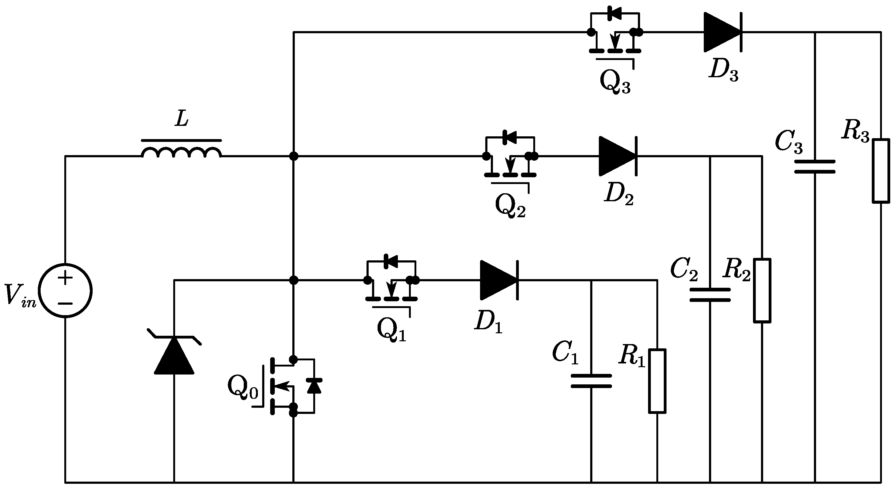
2. SI-SIMO Boost Converter

2.1. Topology

Derived from basic boost DC-DC converter, a single-inductor single-input multiple-output (SI-SIMO) DCDC converter is shown in Figure 1. Different from the traditional boost converter, the output stage is divided into three ports by separate unidirectional switches, which are composed of a MOSFET and a diode. The inductor discharge interval is divided into three by switching on Q1~Q3 sequentially. Switch Q0 is modulated to charge the inductor, resulting in the overall power regulation in the circuit.
Each output port is a voltage source represented by an RC circuit. The equivalent load resistor varies dependently in variable load conditions. This topology requires only one inductor to feed current to three outputs by adjusting the turning-on intervals for each production.
In practical experimental circuits, real-world electronic devices inherently require finite time intervals to transition between on and off states. In voltage source inverters, to prevent shoot-through resulting from simultaneous conduction of Q0 and Q1, a dead-time interval is typically incorporated into their respective PWM control signals. This dead-time implementation ensures a brief period where both switches remain in the off state following Q0’s turn-off and preceding Q1’s activation. However, this protection mechanism introduces a critical operational challenge. As derived from the fundamental voltage–current relationship of inductors L d i d t = V , the abrupt cessation of inductor current during dead-time intervals induces significant voltage spikes across the inductive load. Such transient overvoltage phenomena pose substantial risks of component failure, including potential damage to MOSFETs, diodes, and associated circuit elements.
To mitigate this hazardous condition, a transient voltage suppression (TVS) diode is strategically integrated into the circuit topology. This protective device functions by clamping excessive voltages during transient events, thereby maintaining operational voltage levels within safe thresholds and safeguarding sensitive components from overvoltage-induced degradation.

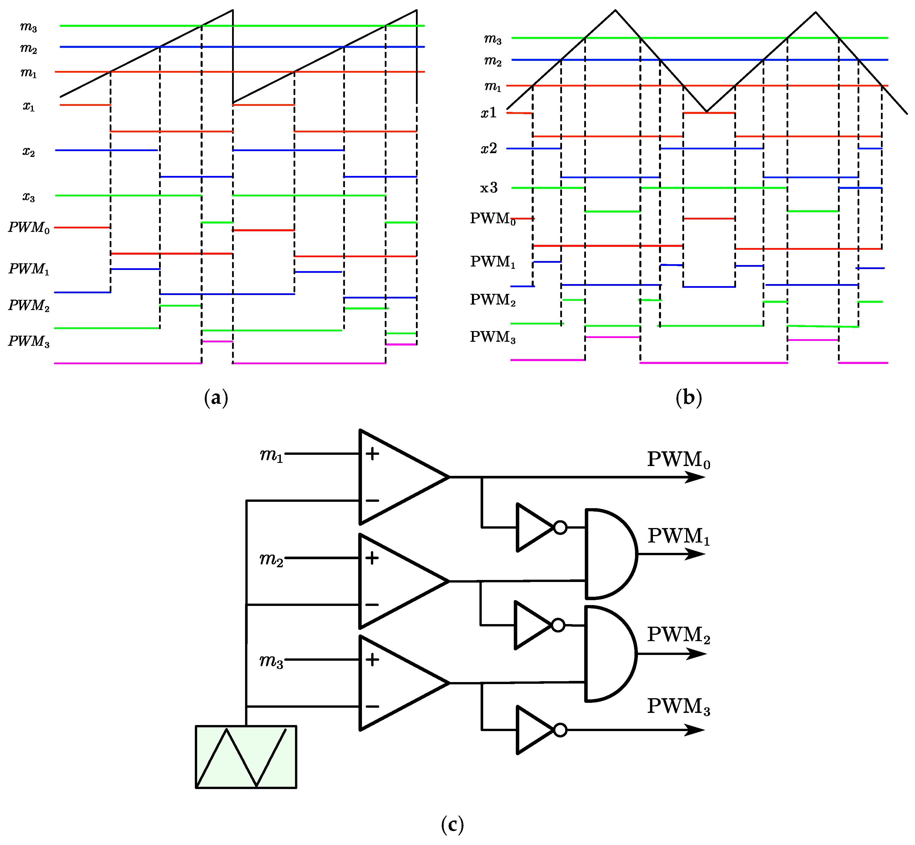
2.2. Modulation Scheme

There are two types of carrier waveforms commonly employed, the sawtooth carrier and the triangular carrier, both utilized for generating PWM signals. The sawtooth carrier waveform linearly ascends from an initial value to a maximum before rapidly resetting, repeating cyclically. As shown in Figure 2a, during the generation of the PWM signal, the modulation signals m1, m2, m3 are compared with the sawtooth carrier via a comparator. When the amplitude of the modulation signal exceeds that of the carrier, a high-level output is produced; conversely, a low-level output is generated, thereby forming an initial PWM signal with single-edge modulation (x1, x2, x3).
To modify rising edge-aligned logic signals to sequential PWMs logic, x1 corresponds to PWM0 directly, while PWM1 is generated from the AND logic of x1 inversion and x2. With the same method, PWM2 can be generated consecutively. The whole process and logic circuit used for this generation is shown in Figure 2c. Generally, this logic used for sequential PWMs can be modeled (1). The PWM signals shown in arrows is used to drive the switches with gate driver IC logically.
PWM k = x k x k + 1 ,   Where : x k = 1      m k > c t 0      m k < c t
where c(t) is the ramp value of the sawtooth waveform carrier, which is implemented as a digital counter in the microprocessor.
The triangular carrier waveform, on the other hand, linearly rises from an initial value to a maximum and then descends back to the initial value periodically. The process of generating PWM signals with the triangular carrier is analogous to that of the sawtooth pattern. However, due to the symmetry of the triangular waveform, two edges are produced within each cycle, enabling double-edge modulation (named the centrally aligned mode in the digital controller). While PWM signals generated by the sawtooth carrier are simpler to implement, they exhibit higher harmonic content. In contrast, PWM signals generated by the triangular carrier contain fewer harmonics and offer smoother output, making them suitable for high-performance applications.

2.3. Overlap PWM Logic to Avoid Overvoltage

Alternatively, the overvoltage issue discussed in Section 2.1 (Topology) can be resolved through pulse–width modulation (PWM) signal adjustment by introducing controlled overlap time intervals in the gate drive signals of adjacent MOSFETs, as shown in Figure 3b. A brief interval is intentionally allocated to allow simultaneous conduction of both devices. This overlap ensures the smoothness of the inductor current, thereby eliminating abrupt current spikes that induce overvoltage transients. Additionally, this strategy reduces system costs by minimizing reliance on voltage-clamping components (e.g., TVS diodes) and mitigates power losses associated with voltage regulation, ultimately enhancing overall conversion efficiency.
It should be noted that the overvoltage can also be eliminated by removing the active switch from any of the output branches. In this way, the inductor current has a backup path to delivering power to the highest voltage output. However, that requires the specific output always be the highest voltage. Otherwise, the other two outputs cannot be boosted higher than that since the branch cannot be actively disconnected from the inductor. In this paper, for its specific application requirements, the output voltage varies for different load conditions. Hence, we keep the flexibility of the circuit output and consider the overvoltage in this circumstance, as well as the protection solution.

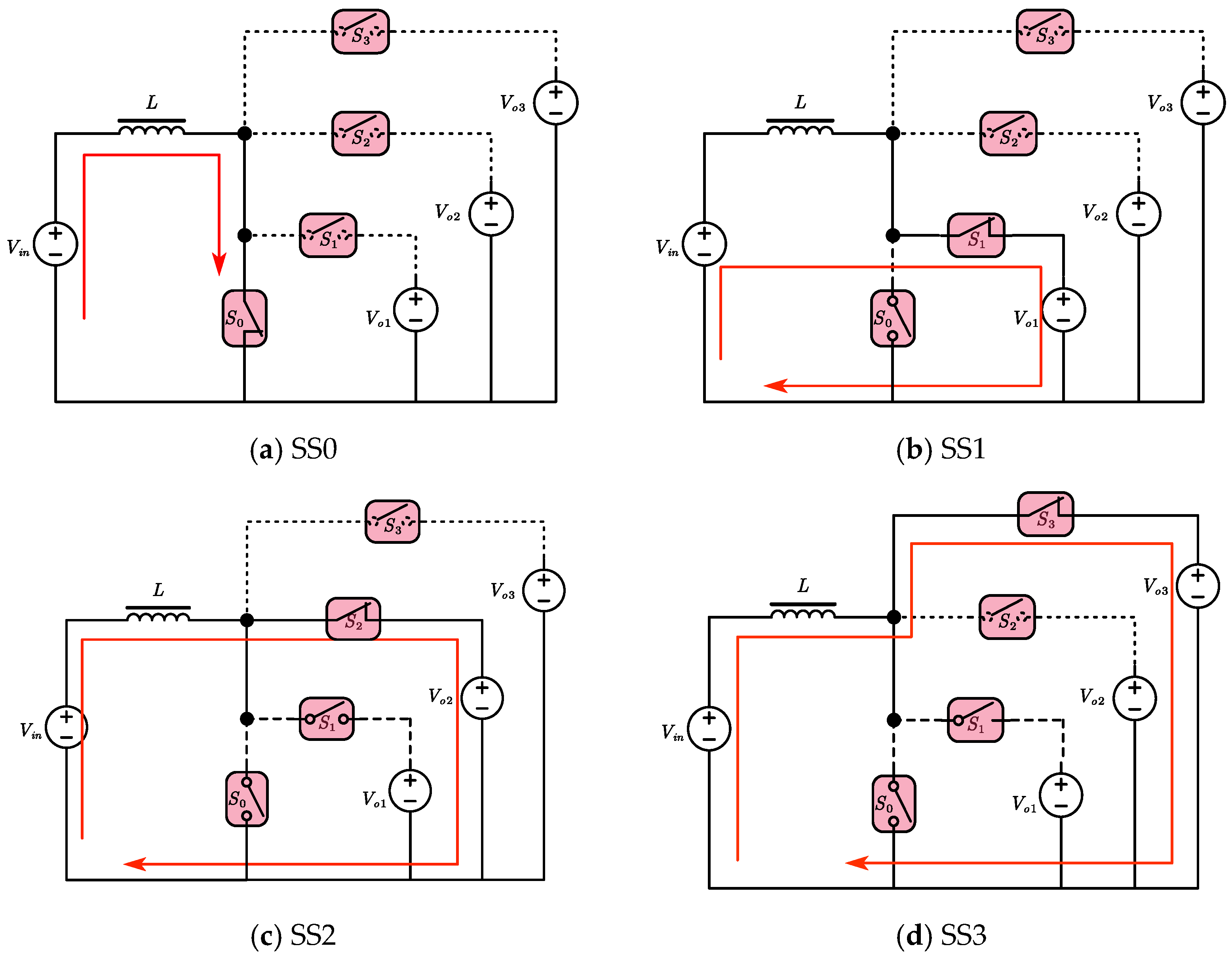
3. Switching-State Analysis

From the introduction of the SI-SIMO topology in Section 2, a switching-state analysis and circuit model derivation are presented in this part. This result determines the dynamic performance and evaluation of circuit design regarding the steady state and transient process In practical circuit design, due to the existence of various parasitic parameters in physical components, failure to account for their influences would result in significant discrepancies between experiment models and actual circuit implementations. Therefore, as shown in Figure 4, the following refinements are implemented in the circuit modeling:
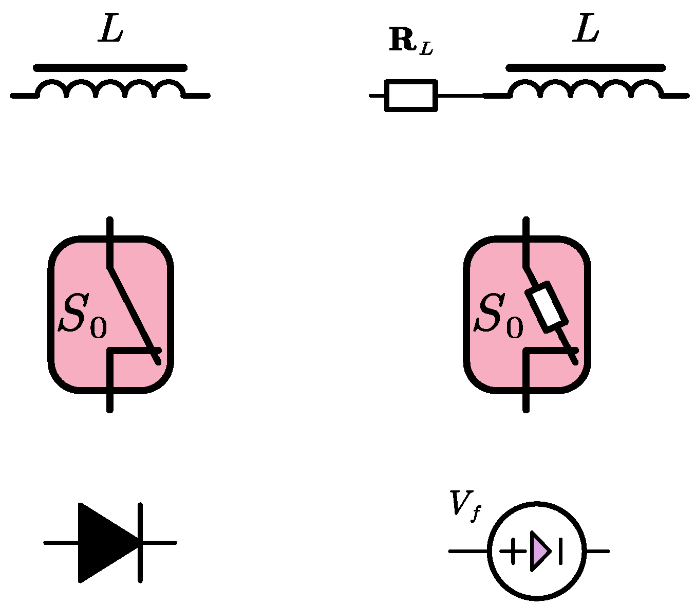
  • Inductor model enhancement: The conventional inductor is replaced with a composite structure comprising an inductor in series with a resistor. This modification explicitly accounts for the parasitic resistance inherent in practical inductors.
  • MOSFET parasitic resistance incorporation: The MOSFET device is represented by an equivalent model incorporating series resistance, graphically depicted as a switch–resistor combination. This refinement quantitatively captures the influence of the MOSFET’s on-state resistance.
  • Diode forward voltage characterization: The ideal diode model is substituted with a unidirectional voltage source element. This substitution effectively models the non-negligible forward voltage drop characteristic of semiconductor diodes during conduction.
With the sequential PWM signals, the proposed SI-SIMO boost circuit has four switching states, shown in Figure 5. The inductor and output capacitors satisfy differential equations for its instant dynamic characteristic.

3.1. Switching-State 0 (Figure 5a SS0)

In this switching-state condition, switch S0 is closed (the corresponding MOSFET is turned on, and the rest of them are turned off). As shown in Figure 5a, the inductor is charged by the input voltage, and the three outputs are RC circuits with a specific initial voltage on each capacitor. Explicitly,
L d i L d t = v i n i L R s
C k d ν k d t = ν k R k ,      k = 1 , 2 , 3 .
where Rs = RL + Ron; explicitly, RL is the equivalent series resistance in the inductor and input loop, and Ron is the MOSFET on-state resistance. Cx are output capacitor values and ux are output voltage values with an equivalent load resistor Rx, while Ron is the on-state resistance of both diodes and MOSFETs. This switching state continues for a time interval determined by the switching period Ts and modulation index value m1. We define a duty cycle d0 for convenience.

3.2. Switching-State 1 (Figure 5b SS1)

Following the previous SS0, in this SS1, switch S1 is closed. As shown in Figure 5b, the inductor releases its stored energy, and the current flows through the MOSFET Q1 and diode D1 to the V1 port. The three outputs are RC circuits. Explicitly,
L d i L d t = v i n V f i L R s v 1
C x d ν x d t = ν x R x      x = 2 , 3
C 1 d v 1 d t = v 1 R 1 + i L
where vf characterizes the conduction voltage of diodes in their on-state.

3.3. Switching State 2 (Figure 5c SS2)

Similar to SS1, the second output port V2 is tied to the inductor during the next interval; the inductor and capacitor satisfy the equation below:
L d i L d t = v i n v f i L R s v 2
C x d ν x d t = ν x R x      x = 1 , 3
C 2 d v 2 d t = u 2 R 2 + i L

3.4. Switching State 3 (Figure 5d SS3)

In the last switching state, the third output V3 is tied to inductor with corresponding differential Equations in (10)–(12):
L d i L d t = v i n v f i L R s v 3
C x d v x d t = v x R x      x = 1 , 2
C 1 d v 3 d t = v 3 R 3 + i L
The four switching-state intervals are repetitively applied in the circuit by adjusting the PWM duty cycles. It should be mentioned that the total switching period consists of these four states. Their duration is determined by the other three in the CCM conditions. Hence, the four duty cycles are related by (13).
k = 0 3 d k = 1
The switching-state analysis (SS0-SS3) establishes the SI-SIMO converter’s operational dynamics, with each state governing energy transfer via sequential PWM. This framework enables steady-state and small-signal modeling in Section 4, critical for optimizing design and control performance under varying load conditions.

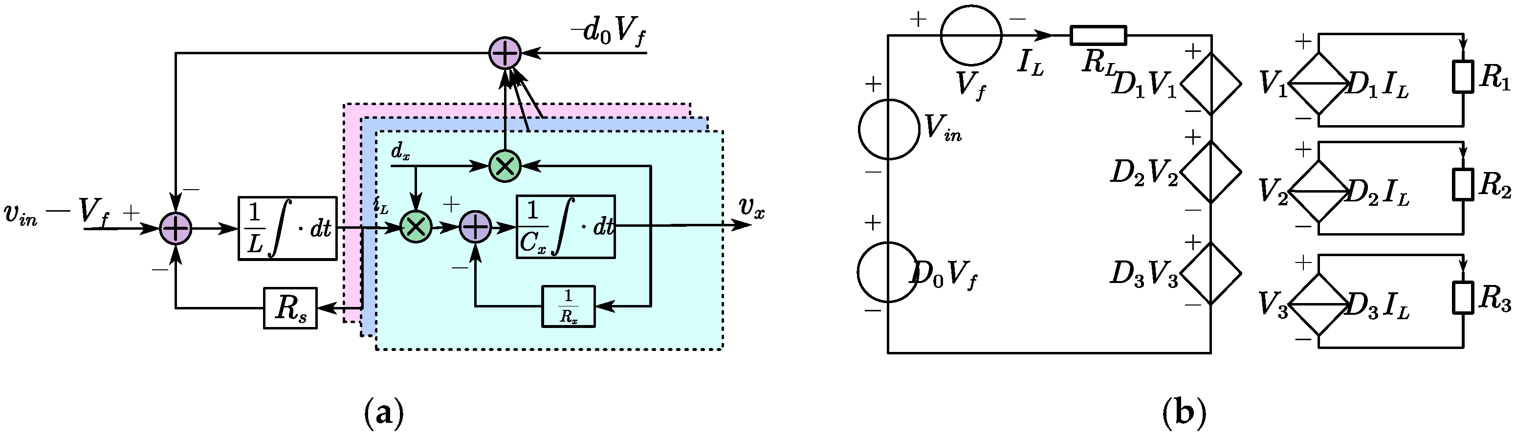
4. SIMO Boost Modeling and Analysis

Different mathematical models are necessary to completely understand the SI-SIMO boost converter behavior. These models help evaluate the converter’s performance regarding dynamic process and steady-state parameters.

4.1. Complete Nonlinear Dynamic Model

By averaging the four switching states with corresponding duty cycles, the inductor current and output capacitor voltage can be derived over a switching period, i.e.,
L d i L d t = v i n i L R s k = 1 3 d k v k + V f
C k d ν k d t = ν k R k + d k i L      k = 1 , 2 , 3
This approach is valid due to the time-scale separation between the circuit’s slow dynamics (e.g., capacitor voltage/inductor current variations) and the high switching frequency. Specifically, the dynamic processes evolve at millisecond-level timescales, while the switching actions induce microsecond-scale ripple. Such separation allows the high-frequency ripple to be neglected without compromising the accuracy of low-frequency system behavior. Consequently, the state variables can be approximated as quasi-static within a switching cycle, enabling the averaged model to retain essential dynamics for stability analysis and controller design. Moreover, this approximation avoids computationally intensive switching details while preserving predictive accuracy for both steady-state and transient responses.
With the averaging modeling approach explained above, the nonlinear circuit model with consideration of some circuit parameters can be drawn as a signal flow diagram, shown in Figure 6a. Since this dynamic model is represented in differential equations with nonlinear properties, an integration block is used for circuit-state transferring instead of the s-domain diagram as a linear system representation. Explicitly, the inductor current is a first-order system driven by the average voltage across the inductor. On the other hand, the three output voltages are driven by the inductor current and the related duty cycle by which the output capacitor is charged. It can be simplified into a first-order linear system if we consider the second term in (15) as an average input. However, due to the three outputs sharing the same inductor current multiplied by related duty cycles, any disturbance in inductor current must cause output voltage fluctuation. In other words, the three outputs are indirectly coupled through the inductor current. The output voltage coupling problem can also be seen in Figure 6a, in which the inductor current drives three output voltage with related interval durations; as a feedback effect, any dynamic process on output will change the inductor current reversely and will be coupled to the other output.

4.2. Steady-State Equivalent Circuit

Considering a steady state, the inductor and capacitors are balanced over a switching period. In other words, there is no incremental, on-average inductor current and capacitor voltage in (14) and (15). Consequently, the left-hand side is zero, i.e.,
0 = V i n V f I L R s k = 1 3 D k V k + D 0 V f
0 = V k R k + D k I L      k = 1 , 2 , 3
where Vin and Vk represent the average input voltage and the average output voltage in the steady state, respectively; the same applies to Dx and IL rather than dx and iL.
To facilitate the numerical experiment, the state variables in Equations (16) and (17) are rearranged on the left-hand side and expressed in matrix form, thereby yielding the matrix equation: MX = P. The matrices M and P are explicitly formulated in the following equations:
M = R s D 1 D 2 D 3 D 1 1 R 1 0 0 D 2 0 1 R 2 0 D 3 0 0 1 R 3
P = V i n V f + D 0 V f , 0 , 0 , 0 T
Subsequently, the state variable matrix X can be obtained through matrix inversion:
X = M 1 P
To systematically investigate the steady-state characteristics of the circuit, as shown in Figure 6b, the circuit averaging method is employed to derive an equivalent resistive network composed of power sources, controlled sources, and linear resistors. As indicated by Equation (8), the three output ports are mathematically represented by voltage-controlled voltage sources (VCVSs) regulated by the output voltages and proportionally scaled by their corresponding duty ratios, while the inductor’s current delivery behavior under specific switching states is equivalently modeled as current-controlled current sources (CCCSs) governed by the inductor current and linearly modulated by the associated duty cycles. In this framework, RL explicitly quantifies the intrinsic resistance of the inductor, whereas Vf and D0Vf characterize the forward voltage drop of the diode. This averaged model, rigorously validated under continuous conduction mode (CCM) conditions, captures the steady-state power transfer dynamics with high fidelity, explicitly encapsulating both conduction and switching losses inherent to the circuit components. By correlating simulated power dissipation metrics—such as inductor copper loss and diode forward loss—with theoretical predictions, the model enables precise verification of component parameter selection accuracy while providing a diagnostic basis for circuit health monitoring through anomalies in duty ratio proportionality coefficients or resistance deviations caused by aging or fault conditions.
From Equations (16) and (17), the average inductor current in steady state can be derived as (18). At the same time, the output voltage is determined by load resistance and duty cycles, as well as inductor current in the steady-state condition.
I L = V i n V f + D 0 V f k = 1 3 D k 2 R k + R s
V k = R k D k I L      , k = 1 ,   2 ,   3 .
Additionally, the coupling effect is also observed in an average circuit model, which is proved in matrix M as well as Figure 6b. This results implies the SI-SIMO converter challenge to the control and closed-loop regulation, especially during transient processes.

4.3. Small-Signal Model

By considering the small-signal perturbation, the circuit states can be represented by x = X + x ^ , where x = v i n , i L , v 1 , v 2 , v 2 T with their capital and small-signal counterparts. With the small-signal modeling approach in [28,29,30], the SI-SIMO converter small-signal model can be derived into (20) and (21):
L d i ^ L d t = v ^ i n i ^ L R s k = 1 3 D k v ^ k + d ^ k V k + V f
C k d ν ^ k d t = ν ^ k R k + D k i ^ L + I L d ^ k      k = 1 , 2 , 3
Equations (20) and (21) can be formalized into state-space Equation (22) in a matrix:
x ˙ = A x + B u y = C x + D u
In (22), the input vector is selected as u = v ^ i n , d ^ 1 , d ^ 2 , d ^ 3 T , the state variables is: as x = i ^ L , v ^ 1 , v ^ 2 , v ^ 3 T , and output as y = v ^ 1 , v ^ 2 , v ^ 3 T , while the coefficient matrices are derived as below:
A = R s L D 1 L D 2 L D 3 L D 1 C 1 1 R 1 C 1 0 0 D 2 C 2 0 1 R 2 C 2 0 D 3 C 3 0 0 1 R 3 C 3 B = 1 L V 1 + V f L V 2 + V f L V 3 + V f L 0 I L C 1 0 0 0 0 I L C 2 0 0 0 0 I L C 3 C = 0 1 0 0 0 0 1 0 0 0 0 1 D = 0
According to the small-signal modeling process, as shown in Figure 7, the perturbation response in the SIMO converter is represented as a linear, multi-input multi-output (MIMO) system, as well as coupling terms between state variables. Small-signal circuit models are widely employed to analyze nonlinear electronic devices under small perturbations around a steady-state operating point. Their primary advantage lies in simplifying circuit behavior through linear approximation, enabling efficient frequency-domain analysis using linear network theory while neglecting high-order nonlinear terms. These models facilitate performance prediction for amplifiers and oscillators through parameters like gain and impedance. However, their validity is restricted to signal amplitudes where nonlinear effects remain negligible, and they cannot predict large-signal distortion or temperature-dependent parameter variations. Additionally, model accuracy critically depends on proper bias condition characterization.

4.4. CCM/DCM Analysis

To effectively evaluate circuit performance and guide converter design, CCM/DCM analysis is required. Since the parasitic Rs and Vf in the circuit are negligible compared to the port voltage and load resistance, they are ignored in this section for simplicity.
In the continuous conduction mode (CCM), as shown in Figure 8, the inductor current of the circuit remains above zero throughout the entire switching cycle, ensuring a continuous flow of energy. The CCM operation is characterized by two primary phases: Phase 1, the inductor charging phase (where switch S0 is turned on, allowing the inductor to store energy from the input source), and Phase 2, the inductor discharging phase (where switch S0 is turned off, and the stored energy is transferred to the output branches corresponding to the different switching states, maintaining a steady current flow).
In the discontinuous conduction mode (DCM), the inductor current of the circuit rises during the SS0 state of each switching cycle, decreases during the SS1 and SS2 states, and drops to zero during the SS3 state, remaining at zero until the next cycle begins. As shown in Figure 8, the DCM operation is divided into three phases. Note that in the DCM condition, in Phase 3, the inductor current crosses zero and reaches negative values. This is assumed for illustration of the DCM/CCM investigation. In the actual converter, regardless of whether in simulation or experiments, the inductor current will stop by the end of Phase 2 in DCM and keep zero until the next switching cycle.

4.4.1. CCM Criteria

In the first method, as shown in Figure 8, the current ripple during the rising segment is described as ΔiLrise. After that, the current ripple during the falling segment is ΔiLfall, which is an accumulated decrease driven by inductor voltage. From Equations (4), (7), and (19), the current ripple can be linearly derived:
Δ i L r i s e = 1 L D 0 T s V i n
Δ i L f a l l = V i n T s L k = 1 , 2 , 3 D k 1 g k
where gk represent the gain of the corresponding output port. It is assumed that the inductor current continues decreasing below zero crossing (although this does not actually happen due to the presence of the diode).
Based on the definitions of CCM and DCM mentioned above, the circuit operates in CCM if it satisfies the equation
Δ i L r i s e + Δ i L f a l l = 0
Otherwise, the summation in (25) must be negative, and it operates in DCM, i.e.,
Δ i L r i s e + Δ i L f a l l < 0
To explicitly derive the criteria of the inductor current conduction mode, substitute (23) and (24) into (25):
0 = V i n T s L k = 0 , 1 , 2 , 3 D k 1 g k .    g 0 = 0
Since the Vin, Ts, and L are always positive, they do not affect whether the equation equals zero. Therefore, (27) can be simplified and abstracted as λ:
λ = k = 0 , 1 , 2 , 3 D k 1 g k . g 0 = 0
Accordingly, if λ = 0, the circuit will operate in CCM; otherwise, λ < 0, and the circuit operates in DCM.

4.4.2. Critical Inductor Value

Before the converter prototyping, the inductor should be carefully designed. Hence, we find the critical inductor value by which the circuit is operated at critical points between CCM and DCM with rated parameters.
Approximately, the input power equals the output power, that is, the left-hand side in (29) equals its right-hand side:
V i n I L k = 1 , 2 , 3 V k 2 R k
where IL is the average inductor current. Assuming the converter has extreme efficiency, the average inductor current can be expressed in (30):
I L = 1 V i n k = 1 , 2 , 3 V k 2 R k
In the critical condition, the average inductor current equals half of the peak-to-peak inductor current, as shown in Figure 8. From the inductor current ripple analysis, as aforementioned, in CCM, the following formula is satisfied:
I L > 0.5 Δ i L r i s e = 0.5 Δ i L f a l l
Substitute (30) and (23), and the critical inductor value can be derived in (32):
L c = V i n 2 T s D 0 2 k = 1 , 2 , 3 V k 2 R k
This section presents a systematic modeling approach and theoretical derivation to establish the analytical expression (Equation (32)) for the critical inductance value in the SI-SIMO boost converter, based on the principle of energy conservation and inductor current ripple characteristics. The derivation process comprehensively incorporates the dynamic relationships among duty cycle, load parameters, and input voltage, thereby quantitatively characterizing the correlation between critical inductance and circuit parameters.

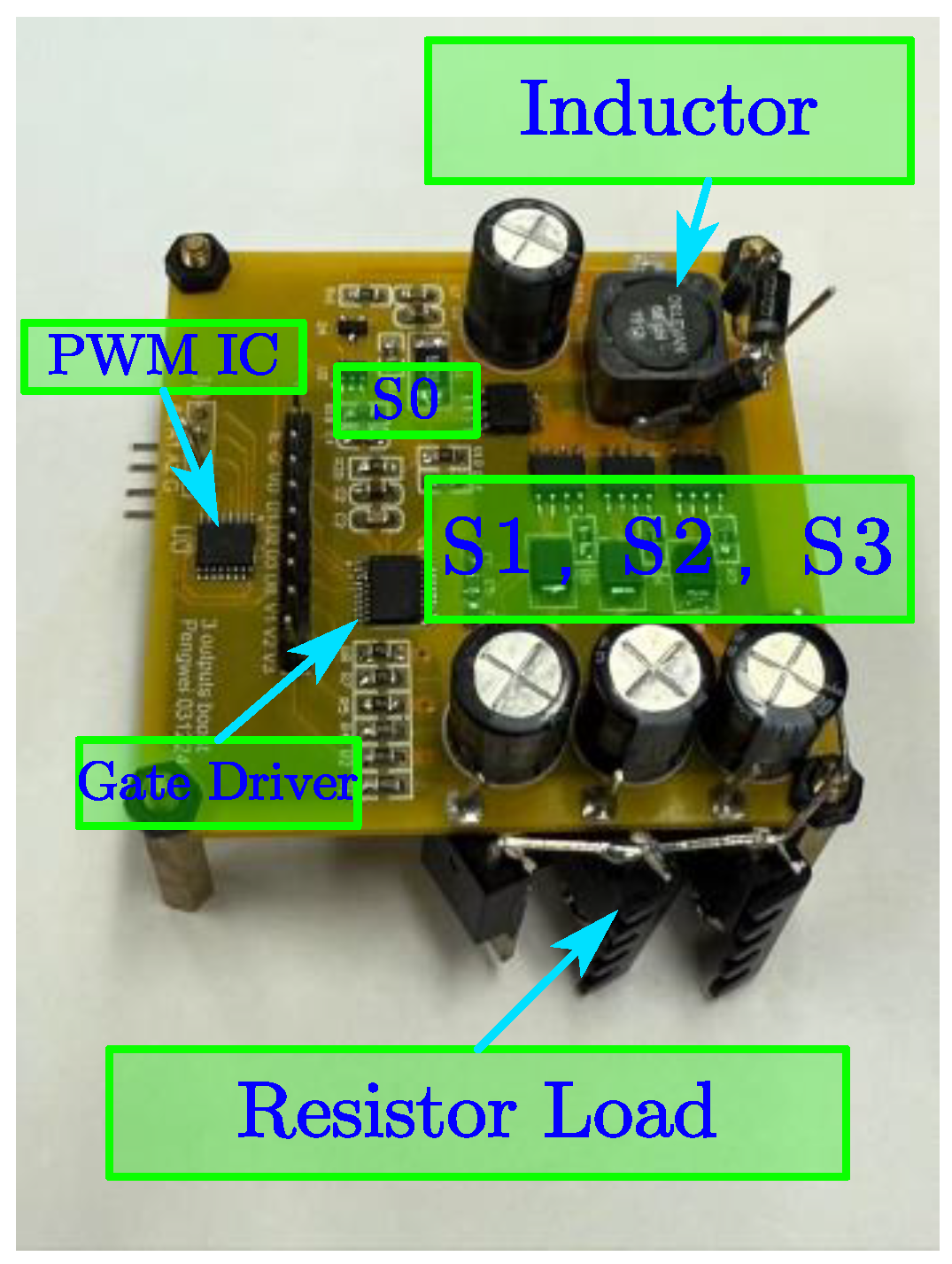
5. Simulation and Experimental Validation

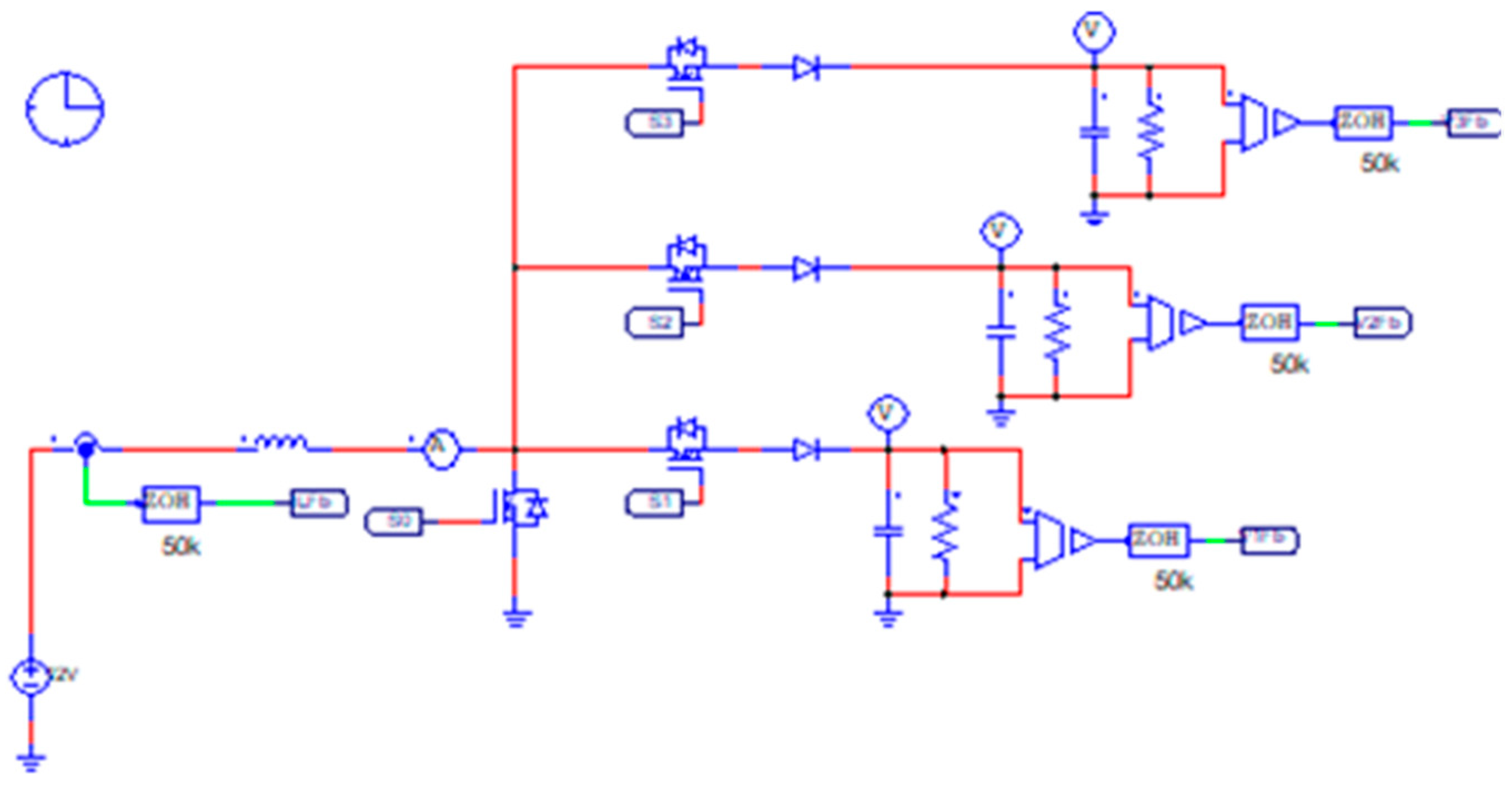
5.1. SI_SIMO Circuit Validation

A switching circuit model is first built in PSIM to validate the topology design and modulation scheme proposed in this paper. In the open-loop control condition, steady-state performance is tested in the PSIM experiment model.

5.1.1. Circuit Model and Experiment Parameters

In this work, an open-loop controlled SI-SIMO DC-DC converter is designed and implemented in the PSIM experiment environment, as illustrated in Figure 9. The circuit features three independent output ports, each capable of delivering distinct output voltages. The core component of the design is a 68 μH inductor, which serves as the primary element for energy storage and transfer. The switching frequency is set to 50 kHz to ensure high-efficiency energy conversion while optimizing the size of the components. To enable three outputs, the output terminal of the inductor is connected to three independent rectifier RC filter branches.

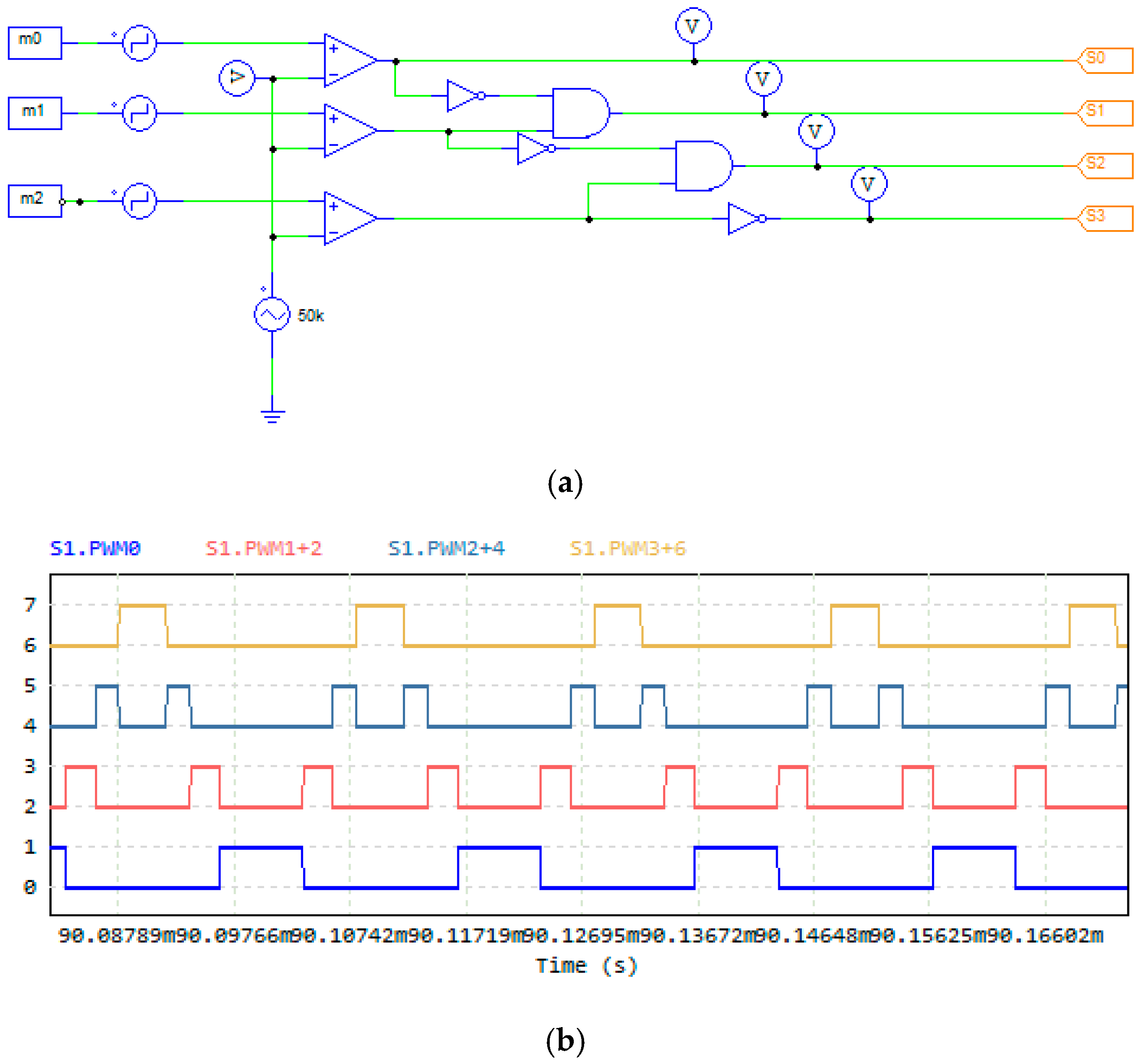
5.1.2. Modulation Logic and PWM Signal

Since the circuit operates under open-loop control, the output voltages are regulated by adjusting the corresponding PWM duty cycle. In Figure 10, the input modulation values m1, m2, m3 are compared with the triangle carrier, which subsequently generates centrally aligned PWM signals. To output the proper sequential switching signals for MOSFETs, the logic circuit is implemented in a specific mode. Sequential PWM signals for switching action are shown in Figure 10b. Note that the triangle carrier generates the symmetrical PWM sequence, and the average current for the four switching states are the same, which improves the accuracy in the derived.

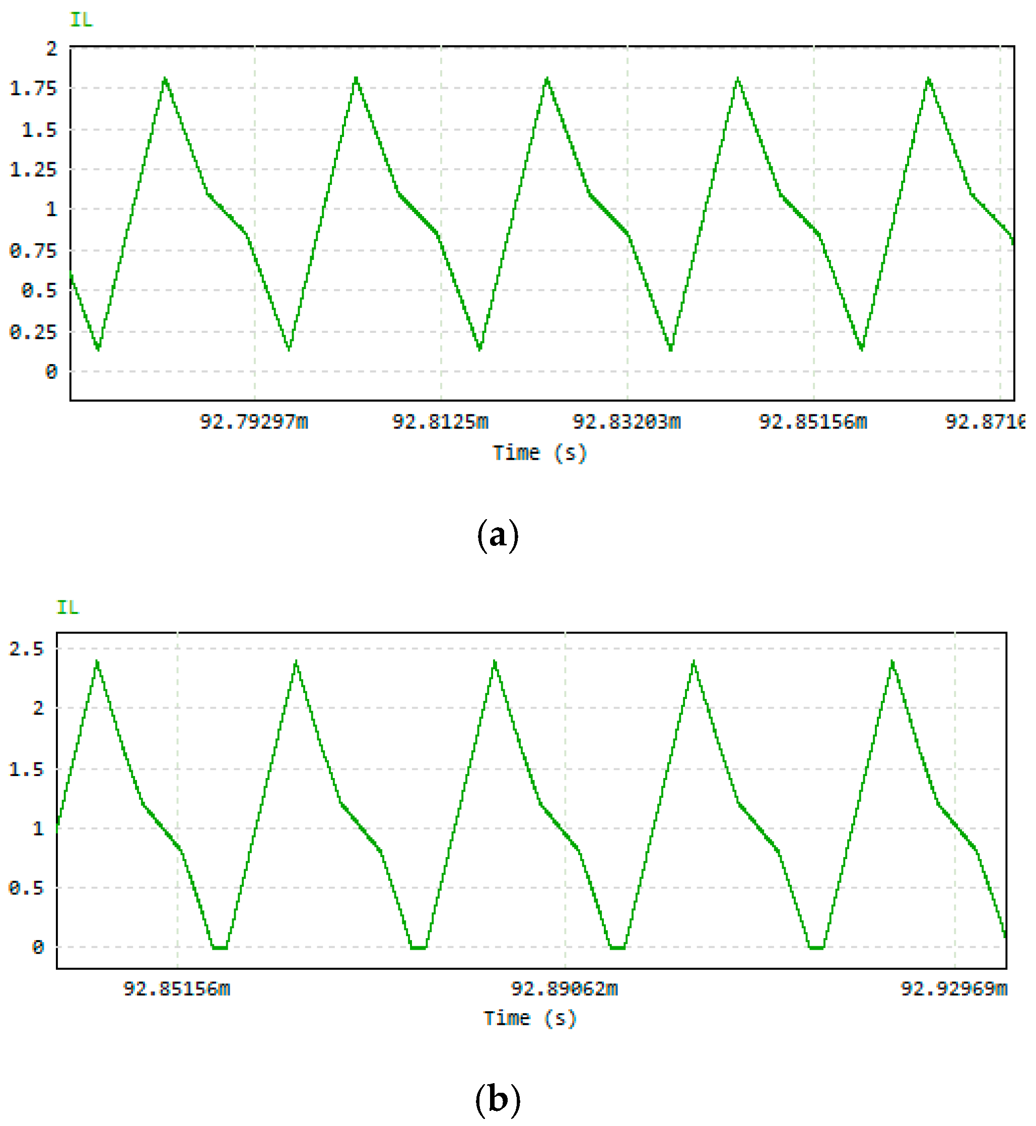
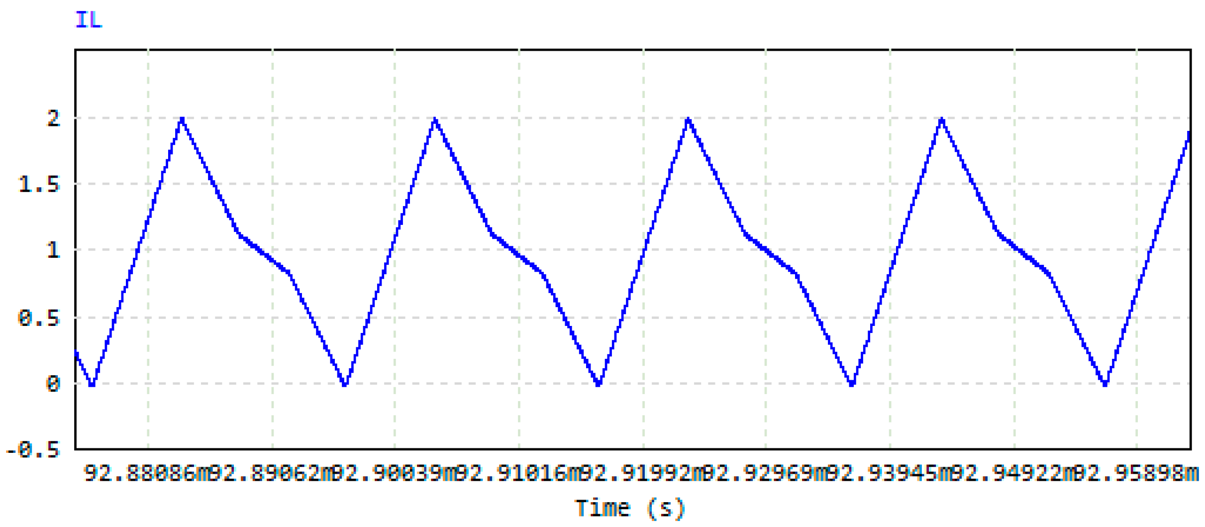
5.1.3. CCM/DCM Simulation

The inductor current waveforms for CCM and DCM are shown in Figure 11a and 11b, respectively. Figure 11a demonstrates CCM operation, where the inductor current remains above zero, ensuring continuous energy transfer. In contrast, Figure 11b illustrates DCM operation, with the inductor current dropping to zero, reflecting intermittent energy transfer under light loads. These results validate the circuit’s modulation principles in CCM and adaptability in DCM.

5.1.4. Critical Inductor Value Simulation

Under the conditions where the duty cycles of the PWM signals for the MOSFETs at each output port are 0.25, 0.2, and 0.2 and the parallel resistance at the respective output ports are 80 Ω, 100 Ω, and 75 Ω, the critical inductance value for the current circuit parameters is calculated in (32) to be 42 μH. By setting the inductor value as 42 μH, as well as the duty cycles and resistor values, the simulated inductor current (IL) waveform is shown in Figure 12. This result indicates a correction in the theoretical steady-state derivation and critical mode analysis.

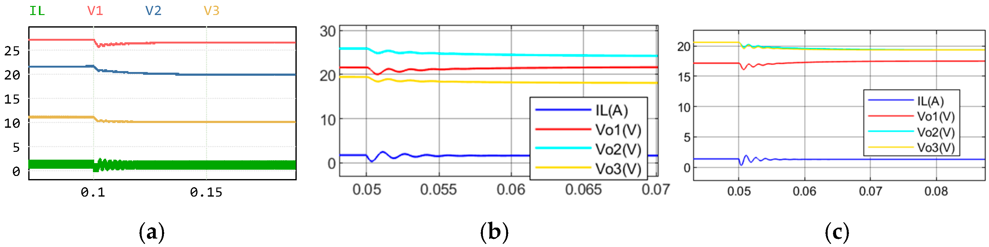
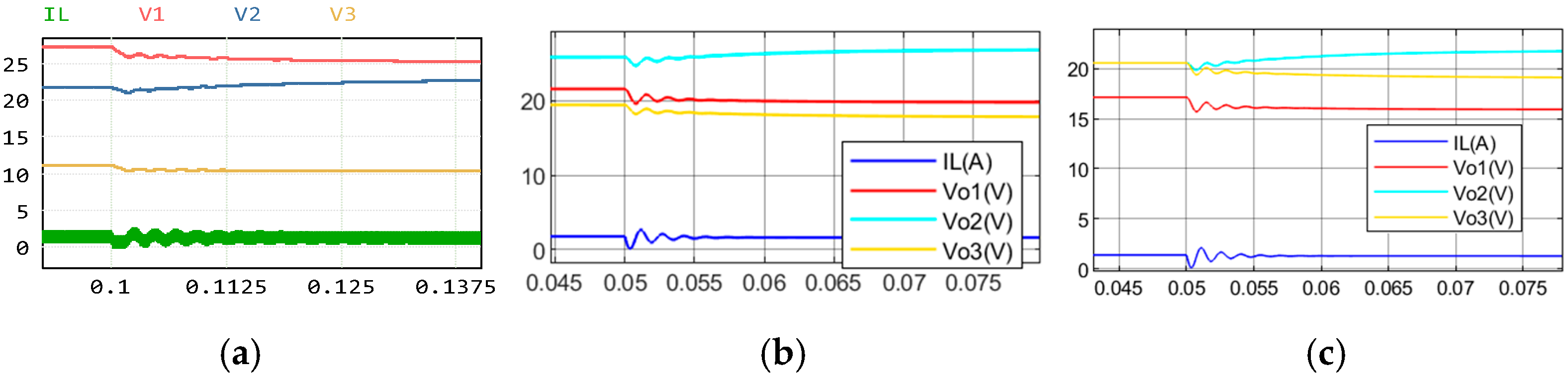
5.1.5. Steady-State Average Test

In Table 1, to verify the steady-state circuit model derived in Section 3, with a specific duty cycle and load resistance, the calculated and simulated output voltage values are compared. For each test condition (the duty cycle and output resistance combination), the upper group value is the calculated output voltage by (19), and the lower group is simulated in a steady state. Considering the diode and switch resistance in the experiment model, the variation between the calculated value and simulated value is acceptable and matches well.

5.2. SI-SIMO Dynamic Modeling Comparison

To validate the SI-SIMO boost converter modeling accuracy, a nonlinear model and a small-signal model at the steady-state operation point are built in MATLAB/Simulink 2024a. By introducing small input perturbations, the state variables’ transient responses are compared between the PSIM switching circuit model and the Simulink model. In Figure 13, the circuit variables are tested with the input voltage step of 12–13 V. It is observed that the inductor current and output voltages are increased with transient dynamics. Moreover, the output voltages are the same proportion since the duty cycle and load resistance are constant in this test condition. In addition, the original nonlinear differential equation model is more accurate than the small-signal model approximation at the static operation point. It is the fact that the original dynamic model includes the all-necessary state variable coupling terms in the equation, whereas the small-signal model is a linear approximation with state-space equations.
Similarly, the transient response is also investigated with perturbation at duty cycle inputs d1, d2, and d3, shown in Figure 14, Figure 15, and Figure 16, respectively. It is worth noting that the small duty cycle perturbation introduced will affect the d0 value to keep the other two duty cycles constant in the derived model and to ensure the entire switching period satisfies d0 + d1 + d2 + d3 = 1. Furthermore, the input duty cycle changes the output power allocation, and the output voltage shows increasing and decreasing between different ports.
The dynamic model experiment on the dynamic and steady-state comparison provides the circuit evaluation before implementation, as well as controller design for high-performance power supply systems. Nonlinear model response and small-signal model approximation help evaluate the linear design margin under certain requirements.

5.3. Experiment

To validate the proposed SI-SIMO boost converter, an evaluation board with an input of 12 V is designed, shown in Figure 17. The single inductor is tied to switch S0 and three unidirectional switches S1~S3, which comprise a diode series with the MOSFET. Sequential PWM logic is generated by and decoded by IC 74HC128. A bootstrap gate driver IC DRV8300D is used to drive the four switches for low-cost consideration. In Figure 18, the three output voltages are monitored in scope. With proper duty cycle step input, the output voltages are changed from one operation point to another, demonstrating the separated output control capability. It is also observed that the three outputs are coupled during the transient dynamics. This result is firmly consistent with the theoretical analysis in this paper and validates the simulation results accordingly. Future research will focus on its closed-loop control and decoupled regulation for its high-performance applications.

6. Discussion

The proposed SI-SIMO boost converter topology and its analytical framework resolve longstanding trade-offs between component complexity, control flexibility, and efficiency in multi-output DC-DC systems. By integrating sequential PWM modulation with a single-inductor architecture, this work achieves independent voltage regulation across multiple outputs—reducing system footprint and manufacturing costs. This advancement addresses critical needs for compact, cost-effective power management in portable electronics and renewable microgrids.
Theoretical contributions include CCM/DCM boundary conditions and a critical inductance formula, providing quantitative tools to suppress voltage ripple and optimize inductor size. A comprehensive modeling framework (nonlinear dynamics, steady-state circuits, and state-space formulation in Equation (12)) quantifies cross-regulation effects.
Practically, TVS diodes and overlapping PWM enhance reliability without snubber-related efficiency losses. The 50 kHz switching frequency supports compatibility with GaN/SiC devices for future efficiency gains. While single-inductor current sharing limits scalability beyond three outputs (applicable to <500 W systems), this aligns with IoT and residential PV auxiliary demands.

7. Conclusions

To fill the gap in distributed power supply in industry applications with existing SISO DC-DC converters, this paper analyzes an SI-SIMO DC-DC converter from a switching-state and modulation strategy perspective. A sequential PWM signal generation logic is proposed. The average circuit model is derived based on switching state analysis. Its steady-state model is discussed, and the CCM/DCM condition is presented. The critical inductor value is derived analytically. With these fundamental analyses, the complete circuit modeling process is derived from a nonlinear dynamic model to a small-signal approximation at the steady-state operation point. An experimental model in PSIM and MATLAB Simulink shows that the proposed SI-SIMO boost converter can independently regulate the output voltage with proper duty cycle inputs with a sequence pulse modulation method. These contribute to prototyping design and circuit performance evaluation. Experiment results validate the proposed modulation scheme and verify the theoretical analysis in different test conditions. From this work, advanced control and implementation solutions can be further investigated in future research.

Author Contributions

Conceptualization, P.M. and J.L.; methodology, P.M., J.L. and Y.Y.; software, J.L. and Y.Y.; validation, J.L. and Y.Y.; formal analysis, H.W.; investigation, J.L. and Y.Y.; resources, J.L. and Y.Y.; data curation, P.M. and H.W.; writing original draft preparation, Y.Y.; writing, review and editing, Y.Y., P.M. and H.W. All authors have read and agreed to the published version of the manuscript.

Funding

This research received no external funding.

Data Availability Statement

The data presented in this study are available upon request from the corresponding author. The data are not publicly available due to privacy restrictions.

Conflicts of Interest

The authors declare no conflicts of interest.

References

  1. Almakhles, D.; Ali, J.S.M.; Navamani, J.D.; Lavanya, A.; Bhaskar, M.S. Single Switch Module Type DC-DC Converter with Reduction in Voltage Stress. IEEE Access 2022, 10, 107877–107887. [Google Scholar] [CrossRef]
  2. Remya, K.P.; Mathew, J.; Nandana, V.S. High Gain Switched Inductor-Capacitor Split Source Inverter. In Proceedings of the 2021 IEEE 2nd International Conference on Smart Technologies for Power, Energy and Control (STPEC), Bilaspur, India, 19–22 December 2021; pp. 1–5. [Google Scholar]
  3. Asapu, S.; Palleswari, Y.T.R.; Rapaka, P.S.; Bade, M.C.; Deenakonda, M.; Banothu, R. Design and Implementation of High Voltage Gain DC-DC Converter for Solar PV Applications. In Proceedings of the 2024 International Conference on Computational Intelligence for Green and Sustainable Technologies (ICCIGST), Vijayawada, India, 18–19 July 2024; pp. 1–5. [Google Scholar]
  4. Das, R.; Le, H.-P. Modular Isolated Vertically Symmetric Dual Inductor Hybrid Converter for Differential Power Processing. In Proceedings of the 2021 IEEE Energy Conversion Congress and Exposition (ECCE), Vancouver, BC, Canada, 10–14 October 2021; pp. 2439–2443. [Google Scholar]
  5. Hamza, A.; Tahir, H.B.; Siraj, K.; Nasir, M. Hybrid AC/DC Microgrid for Residential Applications. In Proceedings of the 2019 IEEE Third International Conference on DC Microgrids (ICDCM), Matsue, Japan, 20–23 May 2019; pp. 1–5. [Google Scholar]
  6. Nayak, P.; Rajashekara, K. A Single-Stage Isolated AC-DC Converter to Interlink Utility Grid and Renewable Energy Sources in a Residential DC Distribution System. IEEE Trans. Ind. Appl. 2021, 57, 4409–4419. [Google Scholar] [CrossRef]
  7. Korobkov, D.V.; Reshetnikov, A.N.; Shtein, D.A.; Geist, A.V.; Sekushenko, T.S.; Klassen, S.V. Simulation of the Multiple Port DC-DC Converter. In Proceedings of the 2017 18th International Conference of Young Specialists on Micro/Nanotechnologies and Electron Devices (EDM), Chemal, Russia, 29 June–3 July 2017; pp. 429–434. [Google Scholar]
  8. Jia, X.; Xu, D.; Du, S.; Hu, C.; Chen, M.; Lin, P. A high power density and efficiency bi-directional DC/DC converter for electric vehicles. In Proceedings of the 2015 9th International Conference on Power Electronics and ECCE Asia (ICPE-ECCE Asia), Seoul, Republic of Korea, 1–5 June 2015; pp. 874–880. [Google Scholar]
  9. Kanaparthi, R.K.; Singh, J.P.; Ballal, M.S. A Review on Multi-Port Bidirectional Isolated and Non-Isolated DC-DC Converters for Renewable Applications. In Proceedings of the 2022 IEEE International Conference on Power Electronics, Drives and Energy Systems (PEDES), Jaipur, India, 14–17 December 2022; pp. 1–6. [Google Scholar]
  10. Li, P.; Silverman, M.; Bazzi, A. Fault-Tolerant Power-Sharing Strategy with A Novel MPPT Method for Parallel PV Converters in Electric Airplanes. In Proceedings of the 2023 IEEE Transportation Electrification Conference & Expo (ITEC), Detroit, MI, USA, 21–23 June 2023; pp. 1–6. [Google Scholar] [CrossRef]
  11. Wang, C.; Sun, D.; Gu, W.; Gui, S. An Adaptive Dead Time Prediction Method for Primary-Side Regulation Active-Clamp Flyback Converter. In Proceedings of the 2022 IEEE Energy Conversion Congress and Exposition (ECCE), Detroit, MI, USA, 9–13 October 2022; pp. 1–6. [Google Scholar]
  12. Xu, C.; Liu, S.; Guo, X.; Xiao, C.; Zou, X.; Zhang, L. A Novel Converter Integrating Buck-Boost and DAB Converter for Wide Input Voltage. In Proceedings of the IECON 2020 The 46th Annual Conference of the IEEE Industrial Electronics Society, Singapore, 18–21 October 2020; pp. 2877–2882. [Google Scholar]
  13. Gevorkov, L.; Domínguez-García, J.L.; Martínez, À.F. Modern Trends in MultiPort Converters: Isolated, Non-Isolated, and Partially Isolated. In Proceedings of the 2022 IEEE 63th International Scientific Conference on Power and Electrical Engineering of Riga Technical University (RTUCON), Riga, Latvia, 10–12 October 2022; pp. 1–6. [Google Scholar]
  14. Verma, H.K.; Mitra, U.; Gupta, A.K.; Mishra, R.; Bhoi, R. Design and Analysis of a Novel Transformer Less Non-Isolated Bi-Directional DC-DC Converter for Applications in Isolated DC Microgrids. In Proceedings of the 2024 IEEE Silchar Subsection Conference (SILCON 2024), Agartala, India, 15–17 November 2024; pp. 1–6. [Google Scholar]
  15. Kumari, D.; Chattopadhyay, S.K.; Verma, A. Multi-Winding Transformer based High Resolution Power Flow Controller. In Proceedings of the 2019 IEEE 28th International Symposium on Industrial Electronics (ISIE), Vancouver, BC, Canada, 12–14 June 2019; pp. 2377–2382. [Google Scholar]
  16. Li, M.; Yu, D.; Yu, S.S.; Li, X.; Geng, H. Enhanced Fault Detection, Localization, and Tolerance Strategy for Dual Active Bridge DC–DC Converters Through Frequency-Domain Analysis of Remote Voltage. IEEE Trans. Ind. Electron. 2025, 1–12. [Google Scholar] [CrossRef]
  17. Villalva, M.G.; Gazoli, J.R.; Filho, E.R. Modeling and control of a three-phase isolated grid-connected converter fed by a photovoltaic array. In Proceedings of the 2009 Brazilian Power Electronics Conference, Bonito-Mato Grosso do Sul, Brazil, 27 September–1 October 2009; pp. 202–210. [Google Scholar]
  18. Kulsangcharoen, P.; Klumpner, C.; Rashed, M.; Asher, G. A new duty cycle based efficiency estimation method for a supercapacitor stack under constant power operation. In Proceedings of the 5th IET International Conference on Power Electronics, Machines and Drives (PEMD 2010), Brighton, UK, 19–21 April 2010; pp. 1–6. [Google Scholar]
  19. Baig, M.J.; Singh, R.K. A Soft-Switched ZVS-ZCS Boost Converter Design and Analysis. In Proceedings of the 2024 IEEE 3rd International Conference on Electrical Power and Energy Systems (ICEPES), Bhopal, India, 21–22 June 2024; pp. 1–4. [Google Scholar]
  20. Ranjan, R.; Singh, P.N.; Karanki, S.B. A Dual-Active-Bridge Based Four-Port Bidirectional DC-DC Converter for Renewable Energy Integration. In Proceedings of the 2023 11th National Power Electronics Conference (NPEC), Guwahati, India, 14–16 December 2023; pp. 1–6. [Google Scholar]
  21. Al-Obaidi, N.A.; Abbas, R.A.; Khazaal, H.F. A Review of Non-Isolated Bidirectional DC-DC Converters for Hybrid Energy Storage System. In Proceedings of the 2022 5th International Conference on Engineering Technology and its Applications (IICETA), Al-Najaf, Iraq, 31 May–1 June 2022; pp. 248–253. [Google Scholar]
  22. Li, P.; Bazzi, A.M. A Three-Port DC-DC Converter for Energy Exchange in Microgrids. In Proceedings of the 2023 IEEE Energy Conversion Congress and Exposition (ECCE), Nashville, TN, USA, 29 October–2 November 2023; pp. 1396–1403. [Google Scholar] [CrossRef]
  23. Li, P.; Nisar, H.; Bazzi, A. Nonlinear Control of A Three-Port DC-DC Converter for Multi-Directional Energy Exchange. In Proceedings of the 2024 IEEE Workshop on Control and Modeling for Power Electronics (COMPEL), Lahore, Pakistan, 24–27 June 2024; pp. 1–5. [Google Scholar] [CrossRef]
  24. Stephen, A.; Remya, K.P.; Gomathy, S. Review on Non-isolated High Gain DC-DC Converters. In Proceedings of the 2022 Third International Conference on Intelligent Computing Instrumentation and Control Technologies (ICICICT), Kannur, India, 11–12 August 2022; pp. 200–205. [Google Scholar]
  25. Lin, R.-L.; Pan, C.-R.; Liu, K.-H. Family of single-inductor multi-output DC-DC converters. In Proceedings of the 2009 International Conference on Power Electronics and Drive Systems (PEDS), Taipei, Taiwan, 2–5 November 2009; pp. 1216–1221. [Google Scholar]
  26. Lodh, T.; Majumder, T. Highly efficient and compact single input multiple output dc-dc converters. In Proceedings of the 2016 IEEE International Conference on Power Electronics, Drives and Energy Systems (PEDES), Trivandrum, India, 14–17 December 2016; pp. 1–6. [Google Scholar]
  27. Solangi, H.; Hafeez, K.; Mekhilef, S.; Seyedmahmoudian, M.; Stojcevski, A.; Khan, L. Advanced Multi-Sampling PWM Technique for Single-Inductor MIMO DC-DC Converter in Electric Vehicles. Energies 2024, 17, 3633. [Google Scholar] [CrossRef]
  28. Pham, N.-S.; Yoo, T.; Kim, T.T.-H.; Lee, C.-G.; Baek, K.-H. A 0.016 mV/mA Cross-Regulation 5-Output SIMO DC-DC Buck Converter Using Output-Voltage-Aware Charge Control Scheme. IEEE Trans. Power Electron. 2018, 33, 9619–9630. [Google Scholar] [CrossRef]
  29. Mohd-Mokhtar, R.; Wang, L. Continuous Time State Space Model Identification Using Closed-Loop Data. In Proceedings of the 2008 Second Asia International Conference on Modelling & Simulation (AMS), Kuala Lumpur, Malaysia, 13–15 May 2008; pp. 812–817. [Google Scholar]
  30. Wang, H.; Sun, H.; Lu, X. An Overview on Small-Signal Modeling and Stability Analysis Methods of Voltage-Source Converter Grid-Connected System. In Proceedings of the 2021 3rd Asia Energy and Electrical Engineering Symposium (AEEES), Chengdu, China, 26–29 March 2021; pp. 320–326. [Google Scholar]
Figure 1. SI-SIMO boost converter topology with TVS diode.
Energies 18 03585 g001
Figure 2. Sequential PWM signals (a,b) and PWM generation logic circuit (c).
Energies 18 03585 g002
Figure 3. SI-SIMO boost converter.
Energies 18 03585 g003
Figure 4. Component parameter considerations.
Energies 18 03585 g004
Figure 5. Switching-state analysis.
Energies 18 03585 g005
Figure 6. SIMO Boost dynamic model diagram.
Energies 18 03585 g006
Figure 7. Small-signal model diagram.
Energies 18 03585 g007
Figure 8. CCM and DCM inductor current ripple profiles.
Energies 18 03585 g008
Figure 9. SI-SIMO simulation circuit model.
Energies 18 03585 g009
Figure 10. Sequential PWM generation: (a) logic; (b) signals with offset value for comparison.
Energies 18 03585 g010
Figure 11. Inductor current ripple in (a) CCM and (b) DCM.
Energies 18 03585 g011
Figure 12. Critical mode inductor current ripple with 42 μH.
Energies 18 03585 g012
Figure 13. Vin 12–13 V step response: (a) PSIM switching circuit, (b) nonlinear dynamic model, (c) small-signal model at static operating point.
Energies 18 03585 g013
Figure 14. D1 0.25–0.27 step response: (a) PSIM switching circuit, (b) nonlinear dynamic model, (c) small-signal model at static operating point.
Energies 18 03585 g014
Figure 15. D2 0.15–0.17 step response: (a) PSIM switching circuit, (b) nonlinear dynamic model, (c) small-signal model at static operating point.
Energies 18 03585 g015
Figure 16. D3 0.15–0.17 step response: (a) PSIM switching circuit, (b) nonlinear dynamic model, (c) small-signal model at static operating point.
Energies 18 03585 g016
Figure 17. Experimental converter.
Energies 18 03585 g017
Figure 18. Open-loop step response (2 us range).
Energies 18 03585 g018
Table 1. Open-loop output voltage comparison.
RX Vx DX[100 100 100][75 80 100][60 90 80]
[0.2 0.3 0.4][18.70 12.47 15.58][12.47 15.58 18.70][21.05 16.84 16.84]
{20.03 12.98 14.91}{13.84 15.60 18.28}{22.29 17.01 16.97}
[0.2 0.25 0.3][16.67 12.85 18.52][10.59 14.12 21.18][18.93 16.15 20.19]
{16.33 11.59 18.04}{11.10 14.14 20.62}{18.64 15.87 19.76}
[0.25 0.2 0.2][15.43 15.43 17.14][9.458 17.73 18.92][17.06 20.47 18.20]
{15.12 15.04 16.73}{9.686 17.49 18.53}{16.74 20.05 17.82}
Disclaimer/Publisher’s Note: The statements, opinions and data contained in all publications are solely those of the individual author(s) and contributor(s) and not of MDPI and/or the editor(s). MDPI and/or the editor(s) disclaim responsibility for any injury to people or property resulting from any ideas, methods, instructions or products referred to in the content.

