Review

Recent Advancements in Understanding Hot Carrier Dynamics in Perovskite Solar Cells

by
Muhammad Mujahid
*,
Jonas Gradauskas
,
Algirdas Sužiedėlis
,
Edmundas Širmulis
and
Steponas Ašmontas
*
Laboratory of Electronic Processes, Center for Physical Sciences and Technology, Sauletekio Ave. 3, LT-10257 Vilnius, Lithuania
*
Authors to whom correspondence should be addressed.
Energies 2025, 18(13), 3543; https://doi.org/10.3390/en18133543
Submission received: 2 May 2025 / Revised: 2 June 2025 / Accepted: 2 July 2025 / Published: 4 July 2025
(This article belongs to the Special Issue Perovskite Solar Cells and Tandem Photovoltaics)

Abstract

A potential field of study for improving the efficiency of next-generation photovoltaic devices hot carriers in perovskite solar cells is investigated in this review paper. Considering their relevance to hot carrier dynamics, the paper thoroughly studies metal halide perovskites’ essential characteristics and topologies. We review important aspects like carrier excitation, exciton binding energy, phonon coupling, carrier excitation, thermalization, and hot hole and hot electron dynamics. We investigate, in particular, the significance of relaxation mechanisms, including thermalization and the Auger heating effect. Moreover, the bottleneck effect and defect management are discussed with an eye on their impact on device performance and carrier behaviour. A review of experimental methods for their use in investigating hot carrier dynamics, primarily transient photovoltage measurements, is included. Utilizing this thorough investigation, we hope to provide an insightful analysis of the difficulties and techniques for reducing the effect of hot carriers in perovskite solar cells and optimizing their performance.

1. Introduction

Metal halide perovskites have remarkable optoelectronic characteristics, such as extended charge-carrier diffusion lengths, adjustable bandgaps, and elevated absorption coefficients, significantly advancing the field of optoelectronics [1,2,3,4,5,6]. Perovskite material is shown in Figure 1a. These materials have intrigued academia and industry due to their significant potential for enhancing photovoltaics. After the preliminary production of perovskite solar cells (PSCs) and attaining a power conversion efficiency (PCE) of 3.8%, research on PSCs has experienced significant acceleration [7]. In a typical ABX3 structure, metal halide perovskites have an A atom for a monovalent cation, like methylammonium (MA+), a formamidium (FA), B cation, like Pb2+ or Sn2+, and X ions for halide anions, like I, Br, or, less commonly, Cl [8,9,10]. An estimate of a compound’s perovskite formation tendency can be obtained from the Goldschmidt tolerance factor (t); nevertheless, a more thorough investigation is always necessary to determine the chemical and thermal stability of the resultant structure [11]. In the case of oxide perovskites that contain transition metal cations, a perfect cubic perovskite is anticipated when t = 1, whereas octahedral deformation is anticipated when t < 1. Electronic properties may be impacted as symmetry degrades for t < 1 [12]. For alkali metal halide perovskites, formability is anticipated for 0.813 < t < 1.107 [13]. The crystallographic structure of perovskite is shown in Figure 1b. A cation with a radius ranging from around 1.60 to 2.50 Å could form a perovskite structure. Since the ionic radius of the methylammonium cation is 1.8 Å, it is an appropriate cation for lead halide perovskites [5]. Solid-state charge-transporting layers have been determined to be compatible with producing high-performance PSCs. Due to committed endeavours over the last ten years, a standard PSC today consists of an inherent light-absorbing perovskite layer, a solid-state n-type electron transport layer (ETL), a solid-state p-type hole transport layer (HTL), a front electrode, and a back electrode. Mainstream device architectures can be categorized into n-i-p (normal) and p-i-n (inverted) topologies [14]. The commercialization of PSCs is hindered by their uncertain stability under long-term operation conditions [15,16,17]. This is a huge obstacle for PSCs competing with the current inorganic photovoltaic (PV) technology. Light [18,19], moisture [20,21,22], and heat [16,18,23] are the three main elements that impact a PSC’s long-term longevity while operating.
Originating in sensitized solar cell material discovery, PSCs have progressed from liquid to solid states [24,25,26]. Along with the ever-increasing efficiency, discussions over the material composition, mechanism of operation, and unusual photoelectric characteristics have persisted. Recent reports have also shown unexpected results regarding the dynamics of second-order recombination and hot carrier (HC) cooling. This cell’s charge-carrier dynamics are the subject of spatial and temporal study in response to these scientific disputes. These dynamics greatly affect device stability, which also decides the device’s efficiency [27,28,29,30]. The energy of sunlight photons is in the 0.5 to 3.5 eV range [31]. When photons have energies lower than the bandgap of a material, they cannot be absorbed and cannot be used [32]. On the other hand, when photons have energies higher than the bandgap, they produce electron and hole pairs with kinetic energy that is greater than that of the lattice one. These pairs of electrons and holes we call the HC [33,34].
One of the most crucial components in deciding the performance of PSCs is the perovskite layer, which is primarily responsible for light harvesting. In addition to its excellent light-absorbing properties, perovskite has demonstrated its ability to carry charge carriers efficiently, providing a firm basis for developing high-performance optoelectronic devices [35,36,37]. The carriers move to the interface between the perovskite and charge transport layers by diffusion across the perovskite layer. This causes recombination and interfacial charge injection to compete, with the charge transport layer being able to retrieve only the victorious. To overcome the Shockley–Queisser (S-Q) limit, the next generation of hot-carrier solar cells must include perovskite characteristics, one of which is the gradual cooling of the charge carriers [38,39]. Initially, free carriers and excitons can be excited and generated at 10:1 within a time frame of less than 2 ps. The exciton in MAPbI3 has been identified as a Wannier–Mott type, exhibiting a weak binding energy in the range of 20–30 meV. This value is comparable to the thermal energy, kbT which is approximately 26 meV, indicating that the exciton can easily dissociate into free carriers at low temperatures [40,41]. The duration of an extremely rapid transition from localized excitons to free carriers has been measured to be 20 fs. To facilitate exciton dissociation at the interface, this discovery implies that an electron transport layer (ETL) or hole transport layer (HTL) is not required to create a heterojunction with the perovskite layer [42].
The free-carrier generation rate is often sufficient for a semiconductor when the exciton binding energy is equal to or less than the thermal energy (26 meV) [43]. The drift-diffusion model describes the carrier transfer, transport, and recombination processes, which primarily govern the charge-carrier dynamics and device performance [44,45]. The photocurrent output under high bias voltage, where the built-in electric field is weak enough, is largely used to determine the cell’s performance now that the JSC is near the transmittance limit [46,47]. Several tests revealed that the exciton binding energy of lead halide perovskites, notably MAPbI3, was lower than the thermal activation energy kbT = 14–25 meV. As a result, the excitons produced by the light separated on their own after being heated [48,49]. The rate of photo-generated carrier production is defined by a three-body Auger recombination equation, a combination of first-order trap state-mediated charge recombination and second-order non-geminate free carrier recombination.
d n d t = A n + B n 2 + C n 3
where A represents the first-order trap state-mediated charge recombination, B is the second-order non-geminate free carrier recombination, C is the three-body Auger recombination, where n is the charge density, and t is the time. Excitation fluency-dependent time-resolved photoluminescence (TRPL) investigations confirm this expression by showing that, in various excitation regimes, the initial photoluminescence intensity (PL0) depends on the excitation density (n0) in a linear or quadratic fashion [50,51].
This review article will concisely summarise recent findings and developments in carrier dynamics, emphasising the importance of HC in defining device performance. The underlying physical principles that control HC behaviour and their production, relaxation, and recombination processes will be thoroughly studied. This review will devote a significant portion to discussing the special features of metal halide perovskites, which are important for studying HC and can be used in high-performance devices. To provide a complete picture, this paper will also review the methods, benefits, and drawbacks of the most popular experimental approaches used to study HC. Technical obstacles, problems with material stability, and the necessity for enhanced theoretical and experimental methods are among the limitations and challenges that this paper will conclude by discussing. HC research and its use in next-generation devices can benefit greatly from this review’s synthesis of existing information and identifying gaps.

2. Unique Properties of Metal Halide Perovskite

Perovskites are a catchall term for a group of crystals with a comparable structure to that of the original mineral found in the Ural Mountains (CaTiO3). Victor Goldschmidt authored a study on the principles governing the chemistry of crystals [52,53,54]. He includes the following examples of crystals: NaNbO3, SrTiO3, BaTiO3, CaZrO3, CaSnO3, FeMnO3, KMgF3, LaAlO3, and LaGaO3, and he describes them as partially cubic and partially pseudocubic. One of their intriguing properties is that perovskites can accommodate several cations of varying valencies at sites A and B. For commercial uses in electronics and other smart devices, this aids in customizing perovskite materials.

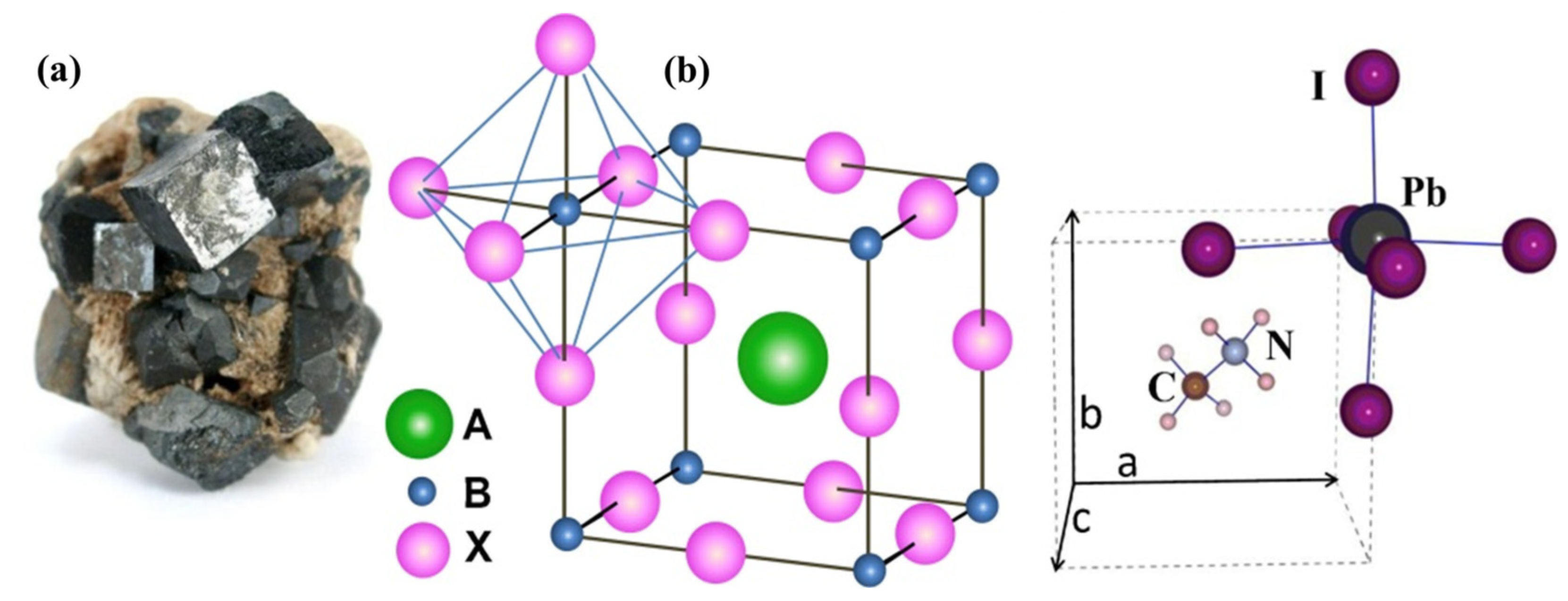
2.1. Perovskite Crystal Structure

Perovski, a Russian mineralogist, found the perovskite in 1839. A generalized crystalline formula of perovskite is ABX3 [55]. Octahedral coordination in a BX6 configuration is applied to the B-site element. In an AX12 polyhedron, the A component is inside the cuboctahedral cavity produced by nearest-neighbor X atoms. Perovskites made of metal halides usually have a monovalent A-site cation and a divalent B-site metal (such as Pb2+, Sn2+, Ge2+, Cu2+, Eu2+, or Ni2+) [56,57,58]. Perovskites formed by trivalent metal halides are rare, yet they can form low-dimensional perovskites [59]. The characteristic feature of 0D perovskites is the presence of organic or inorganic cations surrounding isolated metal halide octahedral anions, with excitons tightly bound to each octahedron. Octahedrons with negative charges form the core, while organic and inorganic cations form the shell; this arrangement can be thought of as a core–shell structure. The first observation of a 0D perovskite structure is Cs4PbCl6, where the surrounding Cs+ cations spatially isolate [PbCl6]4− octahedral [60]. The crystal structure of 0D Cs4PbCl6 is comparable to a 3D structure because of the strong interactions between [PbCl6]4− octahedra. The organic A cation particle size in 3D perovskites is constrained by the dimensions of the 3D hole it needs to fill. The stability of 3D perovskite structures can be predicted using a semiempirical geometric parameter called the Goldschmidt tolerance factor, t [61]. Megaw originally proposed the tolerance factor for perovskite compounds’ stability after investigating various anion and cation combinations [62]. Theoretical framework development was recommended by this study, which covered a variety of perovskite double oxides (cubic, tetragonal, orthorhombic, and rhombohedral, among others). The geometrically enforced requirement for the constituent ions of A r A , B r B , and X r x to be in close proximity for a perovskite structure that is perfectly packed is
t = r A + r x 2 r B + r x
From an empirical standpoint, the range of around 0.81 ≤ t ≤ 1.0 is where most 3D metal halide perovskites arise. Conventionally, NH4CdCl3-type nonperovskite structures are produced when t < 0.8. In contrast, hexagonal structures are usually created when t > 1 [52,63]. Together with the tolerance factor, a second constraint called the octahedral factor (μ) determines the parameter space for perovskite formability. μ is a measure of octahedral stability and is given by
μ = r B r x
and usually falls in the range of 0.44 < μ ≤ 0.9 [64].

2.2. Perovskite Electronic Structure

Understanding a material’s band structure and density of states (DOS) can help to explain its inherent carrier concentration, mobility, recombination mechanisms, excited state lifespan, and other properties important for optoelectronic applications [65,66,67]. The calculation of the conduction band minimum (CBM) and valence band maximum (VBM) for a typical CsPbX3 3D perovskite is performed using the Pb 6p and halogen np orbitals, respectively. Consequently, large band dispersion and low exciton binding energy in the 3D structure of corner-sharing [PbX6]4− octahedra results in simple exciton dissociation [68,69]. The charge carrier effective mass of perovskites determines their carrier mobility, which in turn is influenced by the curvature of their bands in their electronic band structures. The wide band dispersion in 3D perovskites results in a modest charge carrier effective mass, in contrast to the large charge carrier effective mass in 0D perovskites with flat CBM and VBM, which indicates low carrier mobility [70,71]. The band curvature, and by extension, the effective carrier masses and mobility, are affected by the B-X-B bond angles in [BX6]4− octahedra. In their study, Lehner et al. found that, compared with 0D perovskites A3Bi2I9 with Bi-I-Bi angles of approximately 150°, 3D perovskites with nearly 180° B-X-B angles linking the octahedra allowed for better orbital overlap, leading to improved carrier transport through the metal halide lattice [71].
A more recent application of density functional theory (DFT) to the metal halide perovskite system has shown that perovskite band gaps are drastically underestimated, which is common with such approaches. The Pb and Sn perovskite family still lacks accuracy, even after incorporating relativistic corrections such as first-order scalar relativistic density functional theory (SR-DFT) and higher-order spin–orbit coupling density functional theory (SOC-DFT) effects [72]. The electron self-energy/many-body effects raise Eg, while relativistic interactions tend to diminish Eg. As demonstrated in Figure 2a, SR-DFT produces highly exact Eg values for CH3NH3PbI3. Due to the milder relativistic effects with the smaller metal centre, it cannot precisely represent the dispersion of the VB in Pb perovskites, nor does it capture the Eg of Sn perovskites (Figure 2b). As a function of strain and lattice constant, Pb chalcogenides display atypical bandgap variations [73].
The bandgap grows from CsPbI3 to CH3NH3PbI3 to FAPbI3, as shown by Lang et al. [74]. Because of its strong antibonding property, the VBM is projected to decrease as the lattice constant increases. The band structures of Cs4SnBr6 and Cs4SnI6, as determined by DFT calculations, both exhibit a flat band edge, suggesting that the Sn-based 0D perovskites are strongly confining excitons. It was determined that the bandgap of Cs4SnBr6 was 3.33 eV, and that of Cs4SnI6 was 3.00 eV [75]. Not related to halogen np orbitals are the band structures of Cs4EuX6 (X = Br, I) that Wu et al. published. These structures reveal the Cs-6s-derived CBM and the Eu-4f-derived VBM [76]. Strong localization of the Eu-4f orbitals causes the Cs4EuX6 (X = Br, I) to display flat valence band (VB). The predicted bandgaps of Cs4EuBr6 are 3.9 eV, while Cs4EuI6 has a bandgap of 4.2 eV. Although 3D Ge halide perovskites also have direct gap transitions, their 1D counterparts are purportedly materials with indirect gaps that exhibit weak and wide absorption close to the band edge. The composition of the partial density of states (PDOS) around the lowest electronic transition is similar in hybrid and inorganic halide perovskites since neither Cs+ nor molecular A-site cations contribute significantly directly to frontier orbitals [77,78,79].

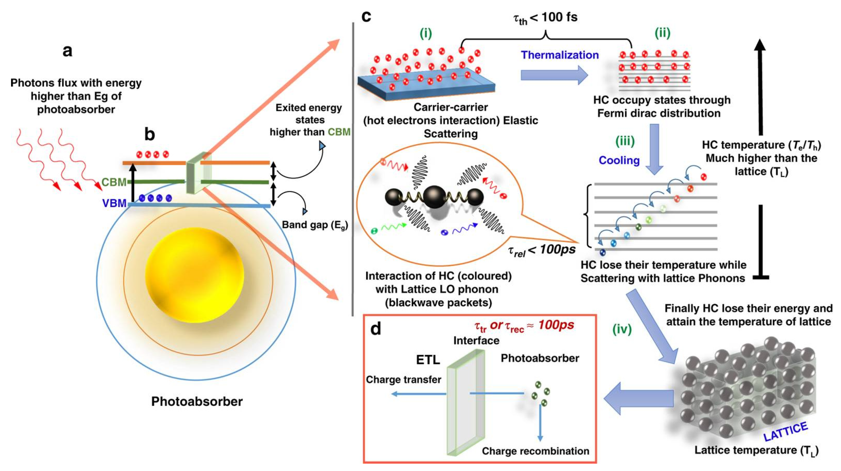
2.3. Carrier Excitation

A pair of free electrons and a hole, also known as an exciton, are produced when light is absorbed. When one or more photons are absorbed, carrier creation can take place. A single atomic electron in a crystal can absorb n photons at once; using Fermi’s Golden rule, we can compute the transition probability Wn.
W n = 2 π ħ M f i 2 δ E f k E i k n ħ ω d 3 k ( 2 π ) 3
where the reduced Planck’s constant ( ħ ), the element of the transition matrix ( M f i ), the photon energy ( ħ ω ), and the energy of the initial (Ei) and final states (Ef) are respective [80,81]. To excite an electron in a photo absorber material to a higher energy level, known as the conduction band, a photon with an energy that is greater than or equal to the bandgap energy (Eg) of the material being excited must enter the material through incident light. When the excitation energy exceeds Eg, the charge carriers go to higher energy states called energy subbands. These subbands are located above the CBM for excited electrons and below the VBM for excited holes. Figure 3 shows that the HCs, which stands for “hot electrons” and “hot holes,” are the charge carriers that are most excited [1,28]. Figure 3a–d shows the step-by-step process of HC production, including the thermalization that follows.
The dominance of second-order non-geminate and third-order Auger recombination in perovskite materials is achieved at an excitation intensity of >1015 cm−3. Investigating the degradation (decay) of time-resolved spectroscopic signals like transient absorbance (TA) and time-resolved microwave conductivity (TRMC) dependent on excitation intensity provides a good window into these higher-order charge recombination dynamics. Surprisingly, the second-order perovskite recombination rates were 2–5 orders of magnitude lower than the Langevin rate [82,83,84]. It is highly probable that recombination is a process triggered by temperature changes. The estimated activation energy for this process is approximately 90 meV [85]. Discussing the kinetics of charge transfer and recombination with organic molecules, such as [6]-phenyl-C61-butyric acid methyl ester (PCBM) and 2,2′,7,7′-tetrakis(N,N-di-p-methoxyphenylamine)-9,9′-spirobifluorene (Spiro-OMeTAD), which are utilized as charge-accepting and transporting electrodes in solar cell systems, is crucial. Previous research has demonstrated that recombination can occur on timescales ranging from nanoseconds to microseconds, depending on the density of carriers [85,86]. Given that Spiro-OMeTAD is extensively utilized as a hole acceptor and transport medium in solar cells, we deduce that hole injection in these devices occurs efficiently on the sub-picosecond timeframe, notwithstanding the absence of the additives lithium bis(trifluoromethanesulfonyl)imide (LiTFSI) or a comparable compound incorporated into this sample. Reports indicate that the preparation method of the perovskite sample can yield either n-type or p-type perovskite [87,88]. Upon light absorption by the bilayer structure, photogenerated holes are transferred into Spiro-OMeTAD, while the electrons remain in the perovskite. The electrons then recombine with the ‘dark holes’ in the perovskite, and the photogenerated holes are introduced into the Spiro-OMeTAD layer.

2.4. Exciton Binding Energy of Perovskite

An exciton, a quasiparticle, can be created in a semiconductor by absorbing a photon with an energy greater than or equal to the bandgap. A strong Coulomb interaction binds the electron–hole pair produced by the light. That is why the exciton-related emission or absorption is observed at energies lower than the fundamental bandgap. It is common practice to use the hydrogen model, which is based on the effective mass approximation in semiconductors, to describe Wannier–Mott excitons, which is the type that is typically seen in perovskites [89,90]. Exciton descriptions in halide perovskites often use both the conventional Frenkel and Wannier models, which is a major consequence [65].
In this scenario, the nth excitonic level’s energy is represented by
E n = E g R n 2
In the present scenario, Eg is the bandgap energy and R is an effective Rydberg for the excitons. Additionally, the lattice screens the carrier interactions. So, the effective Rydberg is just the renormalization of the Rydberg constant, which is Ro = 13.6 eV,
R = R o μ m o ε r 2
where εr is the relative dielectric constant of the crystal, which accounts for the screening of the carriers by the crystal lattice, and 1/μ = 1/mh + 1/me is the exciton reduced mass (mh and me is the effective mass of the hole and electron, respectively) [72,91].
Depending on whether the low- or high-frequency dielectric constant is used, the conventional Wannier–Mott hydrogenic model can yield excitonic binding energies (R = µe4/2ħ ε r 2 ) ranging from 2 to 50 meV, as noted by multiple authors when working with lower mass values (0.1 me) [72,92,93,94,95,96]. Usually utilized in the hydrogenic model for Wannier–Mott excitons in most semiconductors, the high-frequency dielectric constant considers the screening from electronic polarization without including slower ionic contributions. However, because of their strong ionic conductivity and huge dielectric responses, especially under illumination or electric fields, as Yuan and Huang illustrate, halide perovskites offer a more complicated case [29]. Their work shows that ion migration effects, which are not indicative of the screening environment experienced by excitons on ultrafast timescales, allow the static dielectric constant in MAPbI3 to be as high as ~106 at low frequencies (~0.1 Hz). We propose employing the high-frequency dielectric constant (ε∞), which reflects the response of the electronic subsystem only, since excitons in halide perovskites develop and decay on timescales faster than usual ionic migration (which occurs over milliseconds to seconds). This is compatible with the characteristics of Wannier–Mott excitons and with earlier studies separating ionic from electronic contributions to dielectric screening in perovskites. According to the latest findings by Even et al., who fit the line shape of the low-temperature absorption, the exciton binding energy should be around 15 meV. However, when the system transitions to the high-temperature phase, where the photovoltaic cells work, the exciton binding energy drops abruptly to 5 meV due to the additional contribution to the dielectric screening caused by the new rotational motion of the CH3NH3+ cations [93]. Although dielectric screening may change due to dynamic disorder (involving cation rotations), the major effects on exciton binding energy at high temperatures originate from shifts in structural order, widening of the lattice, and different phase changes. Altering the structure changes the number of charge carriers and the static dielectric constant, which is important for calculating exciton binding energy. The findings of Gong et al. indicate that the impact of MA+ rotational motion on exciton binding energy is quite insignificant, and in some instances, it is even negligible [97]. Solid-state hybrid perovskite lead triiodide, whose structure is organized as asymmetric cationic MA+ rotors electrostatically pinned in cages produced by the anionic PbI3 framework, underwent a new sort of electron–lattice interaction, which they referred to as an electron–rotor interaction. From the difference between the 1s and 2s excitonic states, magneto absorption studies revealed the exciton binding energy of various MA and FA lead-halide perovskites to be in the order of 14–25 meV at ambient temperature and approximately 16 meV at low temperatures [98,99]. Furthermore, the binding energy of excitons has also been calculated from optical absorption measurements utilizing Elliott’s model, which permits the disentanglement of absorption contributions from bound excitons and band-to-band fluctuations [100]. Following previous magnetoabsorption investigations, Davies et al. utilized this technique to determine an exciton binding energy of 16 meV for the low-temperature MAPbI3 phase [101]. The Elliott model, like the Wannier–Mott model, postulates electronic transitions between parabolic and isotropic valence and conduction bands; a succession of hydrogenic energy levels characterizes the contributions of bound excitons to the absorption spectrum.
Due to the isolated octahedral structure, the exciton binding energy of 0D perovskites is higher than that of 3D perovskites. Achieving high-performance optoelectronic devices based on photon emission is aided by the strong exciton binding energy, which effectively prevents excitons from dissociating at ambient temperature and the creation of free charge carriers [69,76,102,103]. In their study, Jun et al. measured the PL intensity change of Cs3Cu2I5 with temperatures ranging from 30 to 350 K and found that the high exciton binding energy of 0D Cs3Cu2I5 perovskites was 490 meV [104]. Perovskite nano-crystals (NCs) made of 0D Cs3Bi2I9 were described by Pal et al., and they had a high exciton binding energy of 300 meV [105]. Both the electronic bandgap and the excitonic gap exhibit absorption characteristics because the excitonic state energy (ES) is less than the CBM [105]. Additionally, they discovered that the rate of phonon-mediated relaxation from CBM to the ES is suppressed because the effective phonon energy of 36 meV is significantly lower than the exciton binding energy.

2.5. Phonon Coupling in Perovskite

Understanding and improving the optoelectronic properties of perovskites necessitates a thorough investigation of the phonon modes and their interactions with electrons/excitons. As an example, the light-emitting capabilities of perovskites can be affected by the strong phonon coupling in the materials, which can greatly expand their photoluminescence (PL) [106,107]. Anharmonic vibration typically governs the thermal conductivity, carrier transport, and recombination of perovskite materials via two processes: phonon-phonon coupling and phonon–electron coupling. Figure 2c shows that the phonon dispersion spectral line becomes broader due to anharmonic lattice vibration and the anharmonicity of the atomic force constant, suggesting the coexistence of numerous frequency phonons under a specified wave vector [67,108]. There is a rebalancing of the phonon energy distribution on ultrafast timeframes made possible by energy transfer between phonons when multiphonon states coexist. Figure 2d shows that, due to nonlinear electron–phonon coupling, limited carrier mobility, complicated orbital overlaps between the Pb s-state and halide p-state, and anharmonic structure fluctuation, the VB may be spatially and temporally modulated considerably [109]. 2D perovskites undergo an ordered–disordered phase shift, and Yaffe et al. show that anharmonic thermal vibration significantly affects this process [110]. On the other hand, in 2D perovskites, the iodides would form an anisotropic bonding network with the spacers with the desired configuration, which would create bias in the double well. An additional vibration pattern of the inorganic octahedra at high temperatures is caused indirectly by the interaction between spacers. The several Ag modes in the high-temperature phase result from the same movement of the low-temperature phase, where the bias between the well potential of the octahedra tilts causes an energy difference in the nearby Ag modes. While using theoretical simulations of the vibrational spectra, Quarti et al. were the first to attempt to assign the low-frequency Raman vibrational modes of MAPbI3 [111]. The bending mode of the Pb-I bonds was assumed to be at 62 cm−1 and the stretching mode at 94 cm−1, specifically. Using low-temperature infrared spectroscopy in conjunction with calculations based on first-principles density-functional perturbation theory, Pérez-Osorio et al. examined the vibrational modes of a MAPbI3 thin film in the range of 6–3500 cm−1 [112]. Based on their findings, the Pb-I stretching and Pb-I-Pb rocking modes account for the bulk of the static dielectric constant, whereas the MA cation vibrational modes and PbI3 network’s Pb-I stretching modes predominate in the low-frequency zone. Since the organic cation does not vibrate in the high-frequency range, vibrational analysis of all inorganic perovskites has also been conducted, with a primary emphasis on the low-frequency region [113]. Using Raman spectroscopy and theoretical considerations, Calistru et al. assigned vibrational modes for bulk single crystals of CsPbCl3 in enormous detail [114].
Atoms perturbed from their equilibrium locations experience thermal vibrations that are almost harmonic in conventional semiconductors. Hirotsu and Suzuki conducted the initial studies on the thermal expansion and elastic constants of CsPbCl3 in 1978 [115]. Using temperature-dependent photocurrent (PC) and PL spectroscopy, Phuong et al. explored the exciton–phonon interaction in MAPbI3 single crystals at low temperatures (15–80 K) in another study [116]. Additionally, Diab et al. found that MAPbI3 single crystals had an even lower LO phonon energy of approximately 4.2 meV, accompanied by a strong excitonic emission with a full width at half-maximum of just 5 meV [117]. While research on exciton–phonon coupling has focused on three-dimensional perovskites, a more appropriate platform for studying this phenomenon and addressing the intrinsic relaxation pathways of excitons is two-dimensional perovskites, which have stable excitons as a result of low dielectric screening and quantum confinement and strong Coulomb electron–hole interactions. The layered (C4H9NH3)2(CH3NH3)n−1PbnI3n+1 perovskites studied by Guo et al. demonstrated that acoustic and homopolar optical phonon scatterings dominated the exciton–phonon coupling dynamics, with the scattering rate following a power law Tγ (γ = 1.3–1.9) as a function of temperature [118]. What makes these 2D systems unique is that they did not exhibit polar optical phonon scattering, which is typically the dominant mechanism in highly polar semiconductors. Asymmetric 2D perovskites with large PL line morphologies were also demonstrated in certain investigations [118,119,120,121]. Thirumal et al. discovered that the strong exciton–phonon coupling, leading to the rapid formation of self-trapped excitons (≈100 fs) mainly in the organic lattice, was responsible for the broad emission observed in layered (C8H9NH3)2PbCl4 single crystals, thin films, powders, and solution nanoparticles. The findings show that the organic cation does more than act as a spacer; it also influences the 2D perovskites’ optical characteristics, including their white emission. In conclusion, this section explains how studying 2D perovskites by Ni et al. [119] can shed light on how to modify organic ligands to mitigate the negative effects of strong exciton–phonon coupling in perovskites, which can be a drawback for LED devices owing to PL linewidth broadening and undesirable asymmetric line shape. However, in the second scenario, achieving white-light emission at normal temperature was made easier by broadening the emission resulting from the strong exciton–phonon coupling in 2D perovskites [120]. Strong exciton–phonon coupling could also help with broadband short-pulsed laser development.

3. Fundamental of HC Dynamics in Semiconductor

The photogeneration of an electron–hole pair occurs immediately after a photon with an energy of ħω ≥ Eg is absorbed by a semiconductor with an energy band gap of Eg. A photoexcited electron (hole) with an energy of ħω > Eg is deemed “hot” because its energy exceeds the band gap before any scattering with lattice phonons [122,123,124,125]. Following numerous phonon scattering events, the excited electron (hole) relaxes to the edge of the fundamental conduction (valence) band, releasing its surplus energy as heat. Within the framework of a solar cell, this procedure stands as waste. Consider a Si solar cell with a single p-n junction (Eg = 1.12 eV). When evaluated at 298 K with the standard American Society for Testing and Materials (ASTM) G173-03 global air mass 1.5 (AM1.5G) solar spectra, it exhibited a PCE of 33.4%. Furthermore, there are notable relaxation losses of 47.4%, and the non-absorption of sub-bandgap photons accounted for the remaining 19.2% [124]. Under certain conditions, a new paradigm known as a hot carrier solar cell (HCSC) could be used to collect this surplus energy, as pointed out by Ross and Nozik [126]. By removing the carriers before thermalization, this method could significantly improve efficiency by lowering heat losses. Preventing relaxation requires preventing carrier scattering by phonons [125,127]. The classical hot carrier cell concept is illustrated in Figure 4. It consists of a light absorber containing hot electron gas, two semiconductors with energy-selective connections (ESC) at their interfaces, and the cell itself.
The ESC filters out carriers with specific energies. The suppression of carrier cooling is done while considering Auger and radiative recombination Table 1 summarize the comparison of HC cooling times [1,125,128,129,130,131,132,133]. It is possible to control the carrier density in the bands at the energies of the energy-selective contacts to keep the flux in both directions constant through these contacts by adjusting the doping concentration in the outer semiconductors. When the energy is in a state of thermodynamic equilibrium with the Sun, when radiation from radiative recombination returns to the Sun in each given spectral region according to the detailed balancing principle, the heating will cease. Since the Carnot efficiency can never be surpassed, Figure 4 depicts an ideal solar cell with an inexhaustible thermodynamic efficiency. A solar efficiency limit of 85% or more is attained by optimally driving a reversible heat engine off equilibrium [134,135].
In the solar cell with a single junction, photovoltage consists of two components [136]:
U = U f + U ph
where Uf is the thermoelectromotive force of the hot carrier and Uph is classical photovoltage caused by electron–hole pair generation. A schematic view of the formation of thermoelectromotive force of HC and classical photovoltage caused by electron–hole pair generation is depicted in Figure 5a. It is seen that the polarity of the HC photocurrent is opposite to that of the generation photocurrent. HC photocurrent and generation photocurrent can be observed experimentally by illuminating the p-n junction with the short laser pulse [137].
The temporal profile of the photovoltage across the Si p-n junction induced by 1.489 μm laser radiation is presented in Figure 5b [139]. The fast component has a polarity corresponding to the polarity of thermoelectromotive force of the hot carrier [140]. Since the HC energy relaxation time is much shorter than the laser pulse duration, the leading front of the HC photovoltage Uf pulse follows that of the laser pulse. The calculation of the current–voltage characteristic of a p-n junction under electron temperature approximation leads to the expression of total current flowing across the junction as [136]
j = e D n n p L n e x p e U k T e + e V k k T 1 T T e 1 + e D n p n L p { exp e U k T p + e V k k T 1 T T p 1 }
where e is the elementary electron charge, Dn,p and Ln,p are the diffusion coefficient and diffusion length for electrons and holes, respectively, np and pn are the electron and hole densities in p- and n-regions, respectively, U is the bias voltage, k is the Boltzmann constant, Te and Tp are the temperatures of the electron and hole, respectively, eVk is the potential barrier height of the p-n junction, and T is the lattice temperature. Open-circuit cases when j = 0 and with the equality Te = Tp thermoelectromotive force of HC are equal to
U f = V k ( T e / T 1 )
The thermoelectromotive force of a HC is directly proportional to carrier heating and the potential barrier height of p-n junction.

3.1. Carrier Dynamics in Perovskite

Diodes, transistors, semiconductor lasers, etc., could not have been made possible without precise doping control [141,142]. Naturally, halide perovskite materials and devices must have faults of the same critical relevance. Indeed, halide perovskite can exist in various deep and shallow defect states. Halide perovskites are appealing for inexpensive photovoltaics due to their solution chemistry, and the components, such as iodide, are very reactive, which opens up some other possibilities for doping and the deliberate and accidental formation of defects [143,144,145]. Luminescence quenching and charge trapping are two effects of flaws; luminescence at longer wavelengths reported at low temperatures is another. Shallow flaws slow down the charge transport mechanism because of charge trapping and de-trapping [146,147,148]. This points to the prevalence of phonon-assisted absorption and recombination. The significant carrier-phonon coupling and poor photoluminescence quantum efficiency (PLQE), which are not optimal for optoelectronic applications, could be caused by the indirect character of the transitions. Indirect band gaps were seen in all lead-free perovskite NCs that were investigated, specifically Cs3Bi2X9, Cs2AgBiX6, and Cs2AgSb1−yBiyX6 (0 < y < 1) [149,150,151,152]. The indirect band gap semiconductor Cs2AgBiCl6 has a low PLQE (<0.1% for NCs containing no ligands).
The direct band gap was discovered to be Cs2AgInCl6 [153,154,155]. On the other hand, weak optical absorption coefficients at the band gap result from the parity-forbidden direct transition [156,157]. Due to the slowing down of the cooling process, HC in perovskites have recently attracted significant attention, in addition to the charge carrier dynamics at lower excited states near the band edge. With this, it may be possible to harvest hot charges efficiently, allowing solar cells to surpass the 33% conventional thermodynamic Shockley-Queisser limit [158,159]. At large carrier densities, the cooling rate of hot charges in MAPbI3 perovskites slows down, as previously discovered in early transient absorption (TA) research, which is known as the hot-phonon bottleneck. The considerable carrier re-absorption of optical phonons causes this [160]. While TA investigations provide a wealth of information and may be accessed with great temporal resolution, it’s worth mentioning that these materials have particularly complicated spectra. It is necessary to consider effects such as ground state bleaching, band gap renormalization, state filling, and changing refractive index to conduct an accurate study. Carrier thermalization was reported to occur within 100 fs for short time scales <0.5 ps; values for 1018 and 1019 cm−3 ranged from 10 to 85 fs, depending on the excitation density [41,161]. New research in single-crystal MAPbBr3 and FAPbBr3 microplates demonstrated that the slow hot charge cooling was still true even in the low carrier density regime (<1017 cm−3), which is much below the hot-phonon bottleneck domain. Even perovskites, which are transparent to ultrafast TA microscopy, may transport such high-energy charges across a considerable distance (∼230 nm) [107,162].
According to the growing body of literature on the topic, hot carriers in Pb-based halide perovskites appear to undergo at least two distinct cooling processes. First, the one ranges from subpicoseconds to 2 ps, depending on the sample and analysis method. Given the presence of several cooling stages, and it appears probable that many effects are at play, as the existing explanations for the lengthy heat carrier lifetimes in perovskites are diverse. To dissipate the surplus energy, the following processes must take place: optical phonon decay and acoustic phonon conduction of heat out of the system [38]. In their ab initio calculations, Kawai et al. demonstrated, beginning with the short-term effects and progressing to the long-term implications, that a tiny electronic density of state hinders hole cooling 0.6 eV below the VB maximum in CsPbI3. It was proposed that this effect was independent of the A-site cation, and the equivalent cooling time was found to be 0.5 ps [163]. Using ab initio calculations and ultrafast spectroscopy, Yang et al. also explored the role of the A-site cation. Both hybrid organic–inorganic materials and the Cs-based all-inorganic variation of APbI3 had greater relaxation periods than the other pure APbI3 compositions (MA, FA, and Cs, respectively) [164]. For instance, FAPbI3 showed a relaxation period that was 10 times longer than the Cs version, which agrees with previous findings on CsPbI3 [165].

3.2. The Concept of Relaxation

In a photovoltaic application, perovskite sensitizers absorb sunlight and produce electron–hole pairs with energies well above the band edge. Several factors cause the excited charge-carrier distribution to relax as it approaches the band edge from an initially out-of-equilibrium state. The processes underlying this first charge-carrier relaxation are well-documented for common inorganic semiconductors like GaAs [166]. The characteristics of conventional direct organic–inorganic semiconductors, including high charge-carrier mobilities and low exciton binding energies, have been exhibited by hybrid lead halide perovskites [167,168,169,170]. Increasing the HC relaxation time will theoretically enable the Shockley–Queisser (SQ) limit to be exceeded, and the solar cell efficiency for a single-junction HC-based solar cell under one sun irradiation can be raised to 66% according to a theoretical calculation [126,171,172]. Device performance is strongly influenced by the behaviour and dynamics of HCs inside polar semiconductors. In ordinary semiconductor (like CdSe, GaAs, InN, PbSe, etc.), HC cooling occurs remarkably quickly within hundreds of femtoseconds [27,173,174]. HC can only make a significant impact if t r e is on the scale of radiative recombination. According to the extensive research, if a relaxation time of 1 ns can be reached, a PCE of roughly 50% should be achievable. The thermalization rate Qth, an alternative to t r e , was determined to be 1000 W K−1 cm−2 for bulk GaAs and about 50 W K−1 cm−2 for GaSb-based quantum wells. To achieve a considerable hot-carrier contribution, levels below 1 W K−1 cm−2 are required [38,175,176,177,178].
There are two steps to the HC relaxation procedure. When the HC is not yet in equilibrium, the first step begins with collisions between them, either through electron–hole collisions or, if their concentration is large (>1018 cm−3), through impact ionization and Auger recombination [179]. “Carrier thermalization” is the process leading to the redistribution of excess energy and reaching electronic thermal equilibrium. HC reached the electronic equilibrium in less than 100 fs [135,180,181,182]. When the HC reaches the thermal equilibrium, the second phase of HC relaxation begins. The equilibrium (between the lattice and HC) is achieved through carrier–phonon inelastic scattering. At the picosecond scale, a phenomenon known as “carrier-cooling” takes place [1,182]. Now that the electrons and holes are in their respective energy bands, they can be used for recombination through radiative or nonradiative processes or transferred to the charge transport layers (in PV devices). According to theoretical studies that consider the thermodynamic balance of HC relaxation, equilibration, and extraction rates, the most significant limiting parameters are temperature and the lifetime of the hot carrier [175,183]. Using a simulation, Madjet et al. demonstrated that the relaxation duration of HC in lead halide perovskites is dependent on the composition of the halogens. Using a combination of nonadiabatic molecular dynamics and density functional theory, the impact of cation alteration on HC dynamics in perovskites was investigated [184]. One reason for the low recombination rates in perovskite systems is that hot electrons relax slower than hot holes. This is because the nonadiabatic coupling in the VB states is stronger than that in the conduction band states. The possibility of halide perovskite in hot carrier solar cells (HCSCs) is supported by the long-range HC transport that has been demonstrated in perovskites (up to 600 nm) [38,162,185,186]. A lot of work has gone into studying organic–inorganic lead halide perovskite materials to control the HC dynamics through doping and different chemical modifications, like cation (A+) and halogen (X) alterations [27,187]. The impact of HC cooling dynamics and extractions on Zn-doped CsPbI2Br at a low photoexcitation level (1017 cm−3) was investigated by Xing et al. [188]. Because of its better film structure and lower defect density, the Zn-doped perovskite exhibited a reduced HC cooling rate that was three times lower than that of the undoped perovskite. Furthermore, the delayed carrier cooling and quick extraction at the interface is mostly caused by the nonadiabatic coupling between conduction bands and the introduction of relaxation channels caused by Zn.
A straightforward way to increase the HC lifespan of lead halide perovskite materials is to modify their cations. Nonadiabatic electronic coupling results from charge-state localization around the Cl atom, and a comparable investigation found that slower HC relaxation dynamics are observed when the chlorine (Cl) concentration increases [189,190]. Yang et al. used ab initio calculations and ultrafast spectroscopy to study the A-site cation’s function. The two-hybrid organic–inorganic materials had a longer relaxation time than the Cs-based all-inorganic variant among the three pure APbI3 compositions (A being MA, FA, or Cs) [164]. Madjet et al. computed the HC relaxation in APbI3 in various investigations [191]. The reduced interaction between the Cs cations and the Pb-I frameworks explains why the all-inorganic CsPbI3 exhibited a slower relaxation of both hot holes and electrons and a high dependence on the A-site cation. Single crystals of the bromine variants MAPbBr3 and FAPbBr3 have a HC lifetime surpassing 100 ps (150 and 190 ps, respectively) according to Zhu et al.’s analysis of transient PL spectra, although CsPbBr3 showed no such impact [107]. According to their findings, MAPbBr3 and FAPbBr3 each had a unique carrier cooling phase. By the time 10 ns had passed, the temperature decrease had slowed to 680 K, having begun at 0.5 ns. Furthermore, Talbert et al. investigated how the bromide content in MAPbI3−xBrx affected the excited states and HC dynamics [192]. While an increase in Br concentration has no impact on auger recombination, it does lead to greater electron–phonon coupling and the rapid thermalization of HC. Pure MAPbI3 exhibits a robust hot-phonon bottleneck effect, suggesting an extended HC lifespan, but the phonon bottleneck effect is mitigated by increasing the Br substitution in the crystal lattice.

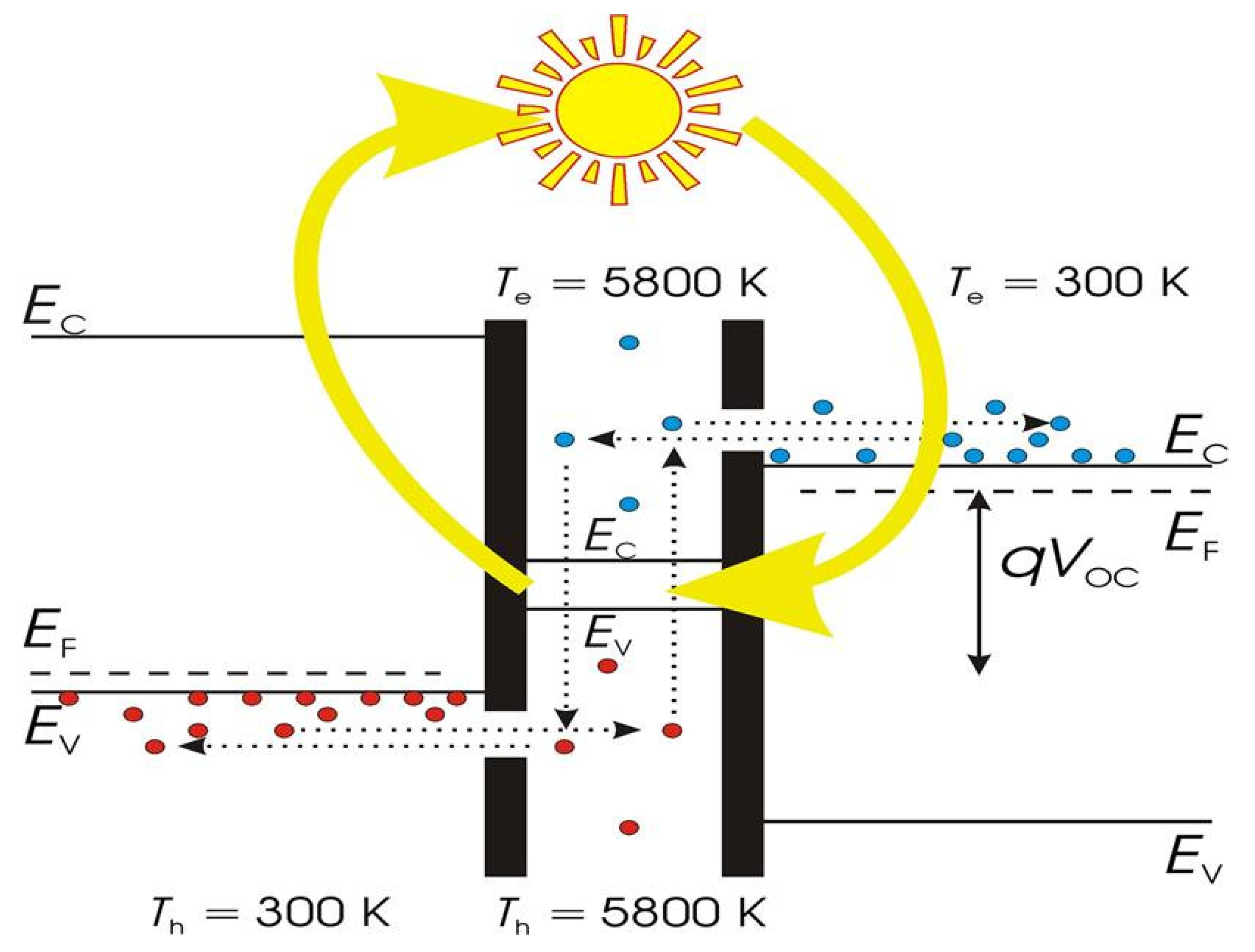
3.3. The Hot Hole and Hot Electron Thermalization

When electrons in a photovoltaic cell are excited from their VB to their conduction band by light, hot electrons and holes are typically created. One must think about the hot-hole relaxation process. The energy diagram depicting hot-hole and hot-electron dynamics is shown in Figure 6 [193]. The sub-picosecond relaxation duration makes it more difficult to collect the hot holes in perovskite thin films using a hot-hole selective layer. This is because, for instance, the hot-hole relaxation time of a MAPbI3 thin film is 100–500 fs, and the hot-electron relaxation time is 1–5 ps [194]. Experimental evidence from transient absorbance spectra demonstrates that the hot holes in a CsPbI3 thin film may be effectively removed by a P3HT thin film capping layer in a matter of 100 fs, which is an excellent development [195]. The HC can only be extracted from photoexcited perovskite NCs using appropriate acceptor molecules. Dursun et al. demonstrated the utilization of spiro-OMeTAD and TiO2 for HC extraction from MAPbI3 NCs [196]. Researchers have used pump–push–probe spectroscopy to study the HC transfer from the higher excited state of CH3NH3PbI3 to bathophenanthroline [197].
Hot electrons cool more slowly than hot holes, according to another study by Zhou et al. [198]. Hot electrons hence have more energy storage capacity than hot holes during cooling. The extraction of hot electrons can thus be expected to maximize the use of solar energy and enhance the PCE of the perovskite. Li et al. first proved the successful extraction of hot electrons. Using ultrafast TA spectroscopy, they investigated the HC dynamics of MAPbBr3 NCs [199]. Ghosh et al. recently showed electron transfer from perovskites to fullerene molecules in a hybrid structure of a dodecahedron CsPbBr3 and fullerene (C60) [200]. For the charge transfer dynamics, bifunctional short-chain aromatic ligands such as 4-nitro thiophenol (NTP) and 4-amino thiophenol (ATP) produce the hybrid structure of 2D Ruddlesden Popper perovskites. According to the findings, hole transfer takes roughly 1.9 ps from perovskite to the ATP molecule, while electron transfer takes 900 fs from perovskite [201]. Alternatively, another study found a hybrid structure involving CsPbBr3 and thiol-functionalized reduced graphene oxide (rGo-Ph-SH) to be an effective extraction method. The HC relaxation time drops from 530 fs in pure CsPbBr3 NCs to 250 fs in a hybrid structure, as seen in the ultrafast transient absorption spectroscopic research [202]. The potential of metal halide perovskites for optoelectronic applications is validated by the significant evidence of effective hot electron extraction provided by all mentioned results.
The MAPbI3 system facilitates the extraction of the hot holes. This is primarily due to the substantial overlap between the localized VB charge of the spiro-OMeTAD molecules and the deep energy levels of MAPbI3 [196]. Therefore, spiro-OMeTAD effortlessly extracts hot holes from the deep energy levels of MAPbI3. It has been reported that CsPbBr3 NCs utilizing 5,10,15,20-tetra(4pyridyl) porphyrin (TpyP) molecules exhibit hot hole cooling and transfer dynamics [203]. According to DFT calculations, the hot hole states are concentrated around the top surface of CsPbBr3, whereas the hot electron states are dispersed away from the top surface. This suggests that TpyP molecules have an easier time extracting hot holes from CsPbBr3 than hot electrons. Reduced interaction between the Cs cations and the Pb-I frameworks indicates that Madjet et al. observed a sluggish relaxation of both hot holes and electrons in the all-inorganic CsPbI3, which is strongly dependent on the A-site cation [191].

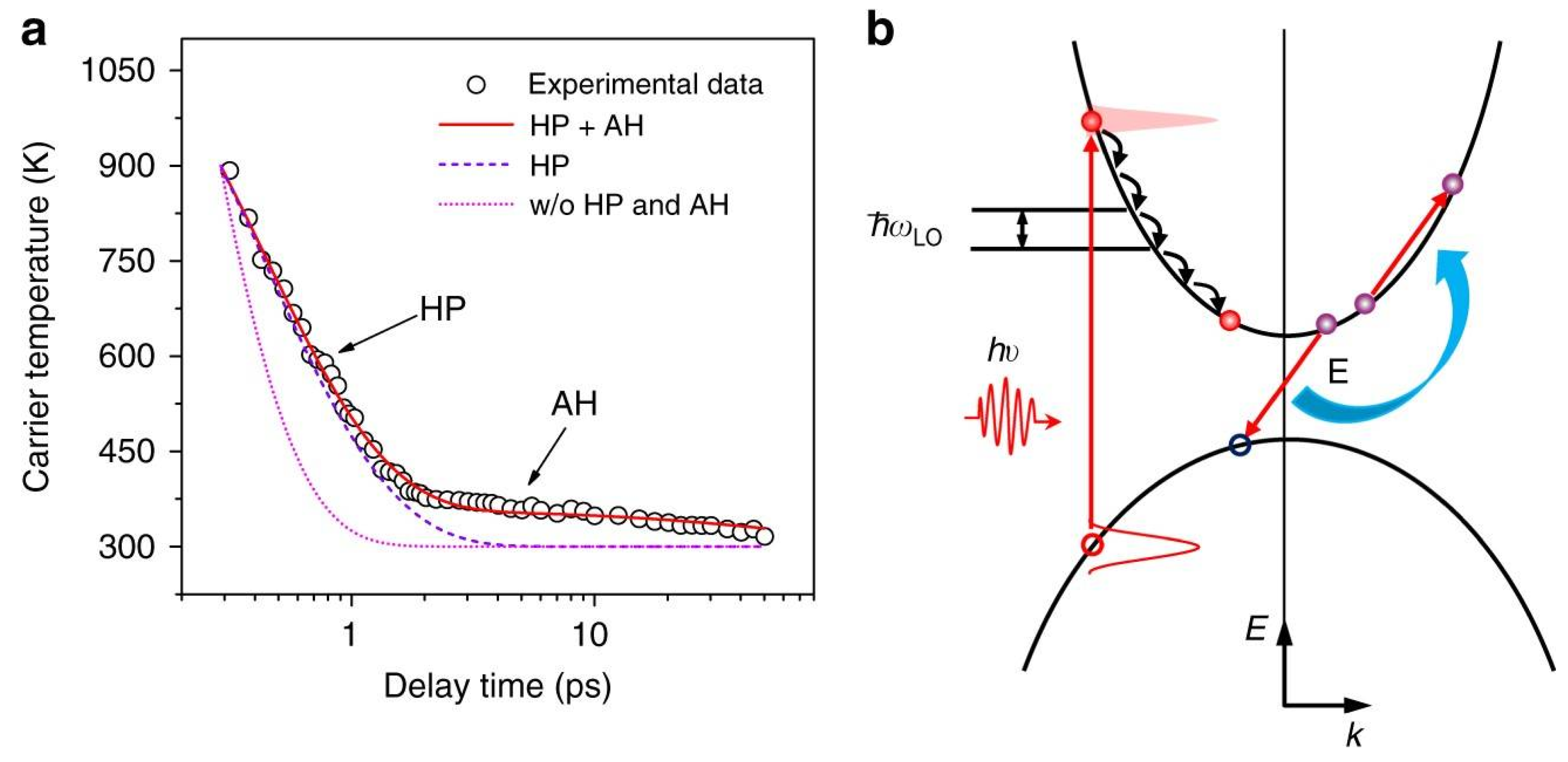
3.4. Auger Heating Effect

In 1925, Pierre Auger made a groundbreaking discovery about gases: the Auger effect. Within an inner shell, an atom becomes ionized. The process begins with an electron falling into the vacancy from an orbit higher up in the atom, and then a second electron absorbs the energy needed to expel it [204,205]. This happens in the very same fashion as solids. Among its traits is the fact that it does not emit radiation. When there is less radiation than anticipated, the Auger effect is suspected, as radiation is what many experiments see. Compared with radiation transitions, it is more challenging to study. At extremely high carrier densities (>1019 cm−3), the Auger heating effect, which is induced by intense carrier–carrier interactions, is a crucial method for monitoring the HC relaxation rate [161,189,206]. Recombination is when an electron–hole pair transfers its extra energy to another carrier, either another electron or a hole, instead of producing light. The receiving carrier’s energy state is raised during this transfer, which may cause more non-radiative recombination processes. The name for this phenomenon is the Auger heating effect [207,208]. Figure 7a shows that hybrid perovskite films can experience a multiparticle Auger-heating effect, further delaying the HC’s cooling to a few hundred picoseconds [130,135]. The energy from electron–hole recombination is transferred to another carrier, which is excited to an even more energetic state, as shown in Figure 7a, as part of the nonradiative Auger-heating process [135,207]. The schematic of the hot electron relaxing process, which leads to the further slowing of hot electron cooling, is illustrated in Figure 7b. This process involves low-energy phonon emission and non-radiative Auger recombination. According to Fu et al., the Auger heating effect was initially described in MAPbI3 films. HC lifetimes can be further extended to tens of picoseconds through the Auger heating effect, according to their findings (Figure 7a) [130].
The carrier relaxation rate is delayed because both carriers use the surplus energy for reexcitation. While the overall energy of the electron–hole (e-h) pair remains unchanged after e-h recombination, the electronic system’s heating can nevertheless make it harder for HC to cool. Eg is the bandgap, and the amount of energy supplied to the electronic system by recombination is directly proportional to Eg + E [209]. The dynamics of carrier cooling, which include the Auger heating effect, can be expressed as follows:
d E d t t o t = d E d t e p h + k 3 n 2 E g + E
d n d t = k 1 n k 2 n 2 k 3 n 3
In this context, n represents the initial carrier density, k1 stands for the monomolecular recombination coefficient, k2 for the free carrier bimolecular recombination coefficient, and k3 for the Auger recombination coefficient; the latter two values are larger for smaller bandgaps and higher carrier temperatures [210]. Equation (8) shows that the first term and the Auger heating contribution by the second term represent the energy loss rate due to electron–LO–phonon interaction. Lead iodide perovskites’ small bandgap and notable hot-phonon impact help to explain their strong Auger-heating effect on HC cooling [135]. The delayed HC cooling time as a result of the Auger heating effect in MAPbBr3 and MAPbI3 NCs was initially observed by Sum et al. [135]. Because there are more Auger recombination processes in CsPbBr3 NCs with an anisotropic hexapod shape, the HC relaxation time is slower [211]. Similarly, in highly excited FAPbBr3 and CsPbBr3 NCs and FAPbI3 NCs, TA spectroscopy revealed delayed HC cooling hindered by the Auger heating effect correlated with a drop in carrier population [189,212]. Although HC cooling lifetimes can be further delayed, the carrier depopulation due to the Auger effect must be carefully considered in order to produce effective HC optoelectronics.

3.5. Bottleneck Effect

In polar semiconductors, a phenomenon known as the “phonon bottleneck” controls the relaxation of HCs. The ‘phonon bottleneck,’ in simpler terms, is when there is an excessively high phonon generation rate but insufficient dissipation or decay pathways for those phonons [213,214,215,216]. The disparity in decay durations between carrier–phonon and phonon–phonon interactions leads to the hot phonon bottleneck phenomenon [217]. A representation of the effect is shown by way of illustration in Figure 8. Reabsorption by charge carriers is more likely due to the nonequilibrium longitudinal optical phonon population that arises from the discrepancy. The hot phonon bottleneck effect basically works in this way to increase hot carrier cooling times. Carriers retain their heat due to the rapid absorption of longitudinal optical phonons, which prevents them from further decaying and turning their energy into heat.
The result is an accumulation of phonons to the point that they are called “hot phonons”, even though any number of phonons, being bosons, can occupy the same energy level. Once optical phonons in this hot phonon population cannot decay due to phonon–phonon scattering, they can re-heat the carriers by going through the opposite emission process called phonon absorption [218,219]. The hot phonon bottleneck effect is predominantly acknowledged for its contribution to prolonged cooling times [81]. Although the term “phonon bottleneck effect” is used interchangeably in perovskite literature, it is crucial to differentiate between the hot and intrinsic phonon bottleneck effects. These words denote separate processes. The quantum dot community is said to be responsible for the intrinsic phonon bottleneck effect. In contrast, the Group III–V and II–VI semiconductor communities frequently exploit the hot-phonon effect [220,221,222]. The physical mechanism underlying the hot phonon bottleneck effect is comprehensively understood for polar semiconductors [217,223,224]. The phonon bottleneck effect is predicted to be stronger in semiconductors having a large phononic bandgap, particularly in bulk materials [173,222,225,226]. The “hot phonon bottleneck effect” was noted in the CH3NH3PbI3 perovskite material when subjected to greater carrier injection conditions, according to Beard et al.’s article in Nature Photonics [27]. They noted that the CH3NH3PbI3 perovskite might be employed in hot carrier solar cells due to the hot-phonon bottleneck effect, which can prolong the relaxation process of the HC. An efficient hot-phonon bottleneck in the lead-iodide perovskite films caused three- to four-orders-of-magnitude reduction in the HC cooling rate at carrier densities larger than 5 × 1017 cm−3. The formula below was used to compute the carrier temperature of the carrier population using a Maxwell–Boltzmann distribution on the high-energy section of TA bleach.
A ħ ω = A 0 ħ ω e x p ħ ω K B T e
The bleach from the high energy component is denoted by ΔA(ℏω), whereas Te represents the carrier temperature. Another group, Deschler et al., noticed the hot-phonon bottleneck effect in the ultrafast transient absorption spectra of organic–inorganic hybrid perovskite materials simultaneously [160]. At very high carrier densities, around 1019 cm−3, the same group discovered that hybrid perovskites exhibited a hot phonon bottleneck effect, which considerably reduced the relaxation time of HC [161]. Herz et al. used temperature-dependent photoluminescence spectroscopy to investigate phonon–carrier interactions in organic–inorganic hybrid perovskite materials; they discovered that, at room temperature, the primary mechanism for phonon-carrier scattering is the Frohlich interaction of longitudinal optical phonons [227].
This effect, important in the study of hot carriers, comes from how the number of existing carriers changes the amount of time phonons live in a semiconductor. If longitudinal optical phonons are the means by which photoexcited carriers lose energy and phonon decay is slow, a large carrier density leads to a buildup of non-equilibrium hot phonons. The presence of many LO phonons keeps hot carriers continuously excited, preventing their cooling until these LO phonons are gone, a phenomenon known as the phonon bottleneck [27,160]. Because of this, the lifetime of the phonons is essential and materials with longer-lasting phonons are likely to be more limited by the bottleneck. Among materials, the hybrid lead halide perovskites FAPbBr3 and MAPbI3 are typical where the phonon bottleneck may develop. It is this sort of dynamically flexible and soft lattice in perovskites that gives optical phonons a tendency to last much longer, especially when photons are introduced in higher numbers. To illustrate, transient absorption and time-resolved photoluminescence studies have demonstrated that a larger number of photoexcited carriers in FAPbBr3 and MAPbI3 causes the carriers to cool much slower, because of the high number of ‘hot’ phonons building up at that time [160]. In perovskites without organic components, like CsPbBr3, the lattice is stiffer and phonons have shorter lives, which helps phonon decay to happen more rapidly and reduces the bottleneck at high carrier densities [189]. However, III-V semiconductors such as GaAs and InP, although able to sustain high numbers of carriers, have shorter lifetimes for phonons because of their stronger and more common phonon–phonon scattering and the less involved nature of their lattice. As a consequence, the problems caused by the phonon bottleneck are greatly reduced and hot carriers relax back to the band edge very quickly, no matter how many there are [27]. The difference makes it clear that lead halide perovskites have unique features, so the lattice properties and cation movements can together make the phonon bottleneck more significant and useful in devices. To sum up, the differences underline that how the phonon bottleneck shows up in different materials depends on the combined effects of the phonon lifetime set by the lattice structure and anharmonicity, as well as the imposed carrier density resulting from excitation of carriers.

3.6. Defect Management

The ability to process perovskites in solutions at low temperatures is a significant benefit, made possible by their low formation energy. Although low-quality polycrystalline films can be formed at low temperatures, this low formation energy impeded the creation of highly crystalline perovskite films. The defect density of these films is much larger than that of a single perovskite crystal, and there are many flaws at the grain boundaries between the crystals [228,229,230,231]. Crystals made of one or two elements are simpler and less prone to deficiencies than perovskites, which are somewhat more complex due to their three-element composition. Different types of defects are defined by the factors that contribute to their production and the structures they exhibit. A few examples of defects in crystal structures include vacancy defects, interstitial defects, and substitutional defects. The former two defects happen when an ion is absent from a lattice site, whereas the latter occurs when an ion occupies an interstitial site [232,233,234]. A significant open-circuit voltage (Voc) deficit and subpar performance are caused by defects, which play the roles of non-radiative recombination centres and ion migration channels. Inorganic metallic salts, organic small molecules or polymers, low-dimensional wide-bandgap perovskites, and ionic liquids are the agents that passivate defect-surplus areas, such as grain boundaries and surfaces [235,236,237]. Also, when one layer is being deposited on top of another, it is easy for flaws to occur on either the top or bottom of that layer. For example, the commonly used electron transportation material C60 can potentially reduce quasi-Fermi level splitting when coated on perovskites by inducing more trap states [237]. Modifying the interface has the potential to prevent defects from forming, reorganize energy alignment, alter carrier selectivity, and improve carrier extraction.
The conversations in previous sections show that the carrier processes in the cell essentially take microseconds. However, the cell has also extensively shown delayed charge processes on the timescale above milliseconds, including the current–voltage hysteresis and time-dependent performance evolution. The general consensus is that certain properties can be adjusted in hot-carrier production and relaxation to accomplish desired goals, like filling trap states, neutralizing charged defects, promoting carrier transport in PSCs, and improving electron–hole separation in the catalysis field. Perovskites can have either shallow traps or deep traps as defects. To classify them, we look at the energy-level disparity (ΔE) between the energetic location of the trap and the band edge. If the energy change (ΔE) is smaller than the thermal energy (kT), where k is Boltzmann’s constant and T is temperature, a shallow trap will be created. By absorbing thermal energy, carriers trapped in a shallow trap can readily escape. On the other hand, a deep trap is created if ΔE is more than kT (i.e., ΔE > kT). Carriers cannot escape a deep trap by absorbing thermal energy. Nonradiative recombination is what they go through [238,239,240]. Also, Yan et al.’s first-principle calculations have projected the defects’ energy levels within the perovskite’s forbidden band [241].

3.7. Critical Analysis of Hot Carrier Dynamics

The hot-phonon bottleneck, in which fast electron–LO phonon coupling outpaces phonon decay, resulting in a non-equilibrium phonon population that reheats carriers and prolongs thermalization times, particularly at higher excitation densities (>1017 cm−3), presents a major obstacle in HC extraction [164]. Furthermore, delaying cooling and complicating extraction, Auger recombination at carrier densities >1019 cm−1 transfers energy from recombining electron–hole pairs back into the carrier population [130]. Interfacial extraction barriers further limit HC extraction by mismatched energy levels at the perovskite–transport-layer interfaces, limiting the collection of high-energy carriers unless state-coupled interlayers are designed [242]. Finally, defects, especially at grain boundaries, act as trap states that capture and disperse heat carriers, lowering the extraction efficiency [243].
A-site cation substitution substantially changes cooling dynamics: perovskites containing organic cations (e.g., FA+) display cooling durations of roughly 0.4–0.5 ps, compared with approximately 0.2 ps in inorganic CsPbX3 counterparts due to improved dielectric screening by dynamic organic cations [244]. Mixed-halide compositions can shorten cooling periods by roughly 30% relative to pure iodide perovskites; halide mixing stiffens the lattice and increases LO–phonon energies, accelerating cooling [245]. Rigid lattices and high electron–phonon coupling in fully inorganic CsPbBr3 produce sub-0.2 ps thermalization, rendering HC signals undetectable [244]. In contrast, the larger FA cations of FAPbBr3 improve phonon screening, extending cooling to roughly 0.5 ps and allowing for strong HC effects. When photons excite carriers in CsPbBr3 and FAPbBr3 perovskites, these “hot” carriers mainly cool by interacting with the lattice vibrations (phonons). However, the detailed steps and duration of cooling are quite different between the two, mainly due to variations in the material’s lattice stiffness, anharmonicity, and how the A-site atoms move. First, we go into detail about why the cooling in CsPbBr3 is rapid and very effective. Carrier–phonon interactions, mostly with shifted optical phonons, bring about the cooling, and this cooling typically happens in the picosecond range. It is possible that, in nanocrystals or quantum dots, the ‘phonon bottleneck’ effect halts cooling, as quantum effects reduce the contact between electrons and phonons. Even though the cooling is faster in hybrid organic–inorganic perovskites MAPbBr3, it is slower than that in regular semiconductors, like GaAs or silicon [27,246]. This is different from FAPbBr3, as dynamic effects and the phonon bottleneck in FAPBr3 allow for prolonged cooling over many picoseconds due to the formamidinium cation. Pure FAPbBr3 films are found to create hot carriers that become free carriers within about 150 fs [247]. Efficient carrier–phonon relationships within the material’s structure cause it to cool very quickly. When FAPbBr3 is linked to IEICO-4F, hot carriers move across about 35 times faster, in just 150 fs, than the relaxed carriers, which need 205 fs. This demonstrates that hot carriers are able to extract more power from the interface [248]. High carrier densities in devices might trigger the hot-phonon bottleneck effect, which can cause the cooling rate to decrease. Even so, the effects are weaker in FAPbBr3 and its ability to cool down rapidly is still present. Hot electrons in FAPbBr3 move out quickly, which may make this material suited for optoelectronic applications.
The difference in HC effect between CsPbBr3 and FAPbBr3 is mainly related to how the A-site cation behaves in each material. The inorganic cesium ion in CsPbBr3 stays put, so it does not participate in dielectric screening. This results in hot carriers strongly coupling with longitudinal optical (LO) phonons. As a consequence, the hot carriers give up their energy very quickly to the surrounding atoms, causing very fast cooling and no obvious effect of hot carriers or bottleneck in phonons [160,189]. The FA+ cation in FAPbBr3 is also larger and able to move easily in the crystal, which causes the local electric fields to change quickly. Thanks to this “dynamic shielding effect,” fewer carriers are transferred to phonons, carrier cooling is slowed down, and the LO phonons stick around longer which creates a clear phonon bottleneck and multi-picosecond hot-carrier lifetimes. The FAPbBr3 lattice has a softer, anharmonic structure, which makes Auger heating a possibility as carriers stay at high levels of energy. Because of this interaction, HCs act differently in the two materials [27,249]. Table 2 illustrates comparative HC dynamics: perovskites vs. GaAs and Si.

4. Experimental Techniques for Studying HC

Engineering the ABX3 perovskite structure with an A-site cation, such as FA, MA, or an inorganic cation (e.g., Cs), has recently become a popular subject in HC dynamics research, leading to the discovery of numerous intriguing principles that can be used to understand the ultrafast exciton and carrier dynamics in greater detail [187,255,256,257,258,259,260]. Most of these investigations found that excitons, when created at room temperature, quickly dissolve into free carriers on a sub-ps time scale, meaning that the free carriers will dominate the following activities. Most of them are related to ultrafast spectroscopy, specifically pump and probe measurements, in which nonequilibrium (electron–hole pairs) are excited by an ultrashort optical pulse and time-resolved spectroscopic measurements are taken at different delays relative to the initial pulse using a second, considerably weaker probe beam [261,262]. Some spectroscopic methods are of special interest to us because of our fascination with the dynamics of electrons, holes, and phonons and how they relate to cutting-edge photovoltaic ideas like hot-carrier solar cells and multi-exciton generation.

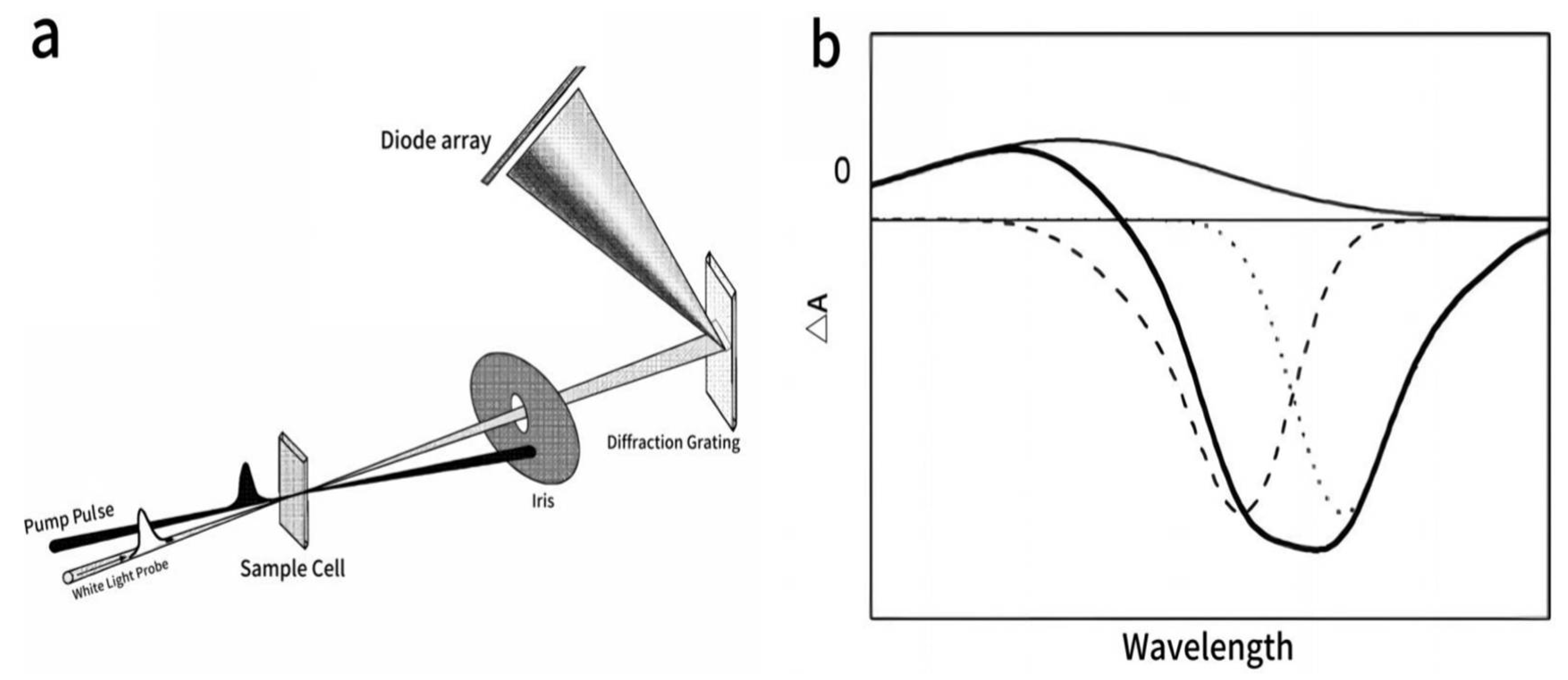
4.1. Transient Absorption Spectroscopy (TAS)

The study of halide perovskite semiconductors, specifically to determine carrier temperatures and analyze the dynamics of HC cooling, has extensively used TAS, a technique commonly employed to examine nonequilibrium processes on an extremely short timescale [27,189,194,263,264]. One well-established method for studying the ultrafast dynamics of photoinduced processes in semiconductor or molecular systems is TAS, which is also called pump–probe spectroscopy. Charge migration, chemical bond formation and dissociation, molecular structure relaxation, and other fast kinetic phenomena in materials and chemical reactions are commonly studied using this technology. Figure 9 shows that TAS utilized laser pumping and probing [265,266,267,268,269,270].
In 2013, Xing et al. used TAS to investigate the higher-energy photobleaching (PB) band (PB1 at ≈480 nm) in MAPbI3 polycrystalline films, which led to the first report of slow HC cooling in halide perovskites in the literature [263]. Due to gradual hole cooling, the band edge bleach signal slowly increases while a deeper-level bleach signal decays simultaneously, with lifetimes of approximately 0.4 ps under pump energy of 3.1 eV. Despite this, Yang et al. still discovered that the TAS of MAPbI3 films, which have a very low exciton binding energy of approximately 9 meV, still need to account for the excitonic impact and exciton contribution [27]. Using excitation densities (n) ranging from 3.8 × 10¹⁶ to 5.5 × 1018 cm−3, the transient absorption (TA) spectra were obtained in this study using the ultrafast pump–probe technique. The findings indicate that the exciton bleach dominates the TA spectrum for an excitation intensity of less than 1 × 1018 cm−3. However, as the excitation densities increase, the Moss–Burstein shift takes over, and the continuous contribution from free carriers becomes more prominent. The conduction band states CB1 and CB2 also showed comparable concurrent rise and decay bleach signals in a subsequent study by Sum et al. This suggests that the hot electron cooling process, which is sluggish, also happens at approximately 0.4 ps [271]. As confirmed by Chen et al., who found that HC cooling rates in MAPbI3−xClx films are dependent on pump fluence and that the ground-state bleaching signals take longer to build up as the fluence increases up to 340 µJ cm−2, the HC cooling rates in MAPbI3−xClx films are even slower, reaching up to ≈10 ps [272] Using TA spectroscopy, G. Motti et al. showed that the MAPbBr3 and MAPbI3 perovskite thin films exhibited defect activity [273]. The photobleach signal should be visible in both films. One possible explanation for the photobleaching signal is that the electron and hole densities in the conduction and valence bands are linked. The result is that this signal allows the study of trap-assisted recombination and radiative and nonradiative recombination routes. Trapped carriers do not cause photobleaching, but they can cause an imbalance in the opposite band, which adds to the photobleaching signal. Many theoretical and practical investigations into the causes and mechanisms of these intriguing delayed HC cooling phenomena were initiated because they fascinated researchers.

4.2. Time-Resolved Photoluminescence (TRPL)

The TRPL is subsequently used extensively to study the carrier recombination process and its lifetime. To measure TRPL, a pulsed light source is employed to excite a sample, and the PL intensity is captured as a function of time from stimulation. British scientist George Porter developed flash photolysis in the middle of the 20th century to study the photolysis of a chlorine and oxygen mixture. This experiment served as the precursor of time-resolved spectroscopy [274]. A mature optical characterisation technique, time-resolved spectroscopy, has developed over fifty years. It is now extensively employed to study a wide range of transient dynamic processes, including electron excitation and relaxation [275,276,277,278]. The accumulated emission-time profiles are significantly affected by factors about the excitation source (current, wavelength, and frequency) and the experimental setup (excitation direction, exposure duration, detection time window, and sample atmosphere) when conducting TRPL studies. Nanosecond laser pulse excitation is a common method for TRPL measurements. Regarding contributions from subnanosecond operations, the pulse width constraint is completely inadequate. Due to differences in excitation laser pulse width, detection timeframe, and nonexponential decay, excited state durations estimated from PL and ultrafast TA measurements may not always match [279]. The material’s characteristics, notably the carrier dynamics, are determined by the dynamics process in perovskites. As a result, the mechanism of photoelectric and luminous behaviour of perovskites can be better understood using time-resolved spectroscopy. MAPbI3 films’ PL lifetimes of ≈10 ns and MAPbIxCl3−x films’ PL lifetimes of >100 ns were associated with the charge carrier population degradation [50,280]. According to one-dimensional carrier diffusion modeling of the PL dynamics, the resulting diffusion length for MAPbI3 polycrystalline films was calculated to be ≈100 nm, with D = 0.017 cm2 s−1 for electrons and 0.011 cm2 s−1 for holes. D = 0.04–0.05 cm2 s−1 allows for the diffusion length to reach 1 mm in mixed-halide MAPbIxCl3−x films [51,281]. Films with greater grain sizes (D = 0.1–2.5 cm2 s−1) demonstrated more efficient charge transport. Trap density, specifically surface/interface defect states, exerts substantial control over carrier transport in perovskites [282]. Further analysis of the D values reveals that the mobilities of the minority carriers are 10−1–10−2 cm2 V−1 s−1. Conversely, while preparing a CsPbBr3 thin film, Jiang et al. studied how surface treatment affected the carrier lifetime [283]. Before applying the CsPbBr3 film to the glass substrate, a thin layer of polyvinylpyrrolidone was spin-coated [284]. There was a clear enhancement in the PL intensity and carrier lifespan in the steady-state PL (SSPL) and TRPL spectra. The carrier lifespan was increased from 3.1 to 13 ns, and the PL intensity was six times better. Studies show that TRPL is among the most often used technologies for investigating charge dynamics in perovskite materials due to the extensive number of detection techniques [285].

4.3. Transient Photovoltage Measurements

Transient photovoltage measurements were used to study carrier heating in InSb using infrared radiation for the first time [286]. The p–n junction was illuminated by the pulses of a CO2 laser with a wavelength of 10.6 μm and a length of 200 ns. The photoresponse of an InSb-based p–n junction during illumination by CO2 laser was composed of two components: the thermoelectromotive force of HC Uf and the classical photovoltage caused by electron–hole pair generation Uph. It was observed that Uph is a quadratic function of laser power density, as the generation of electron–hole pairs in InSb takes place through two-photon absorption of light from the CO2 laser. The thermoelectromotive force of HC was found to increase linearly with increasing laser power density. Later, the transient photovoltage measurements were used to study the HC impact on photovoltage formation in GaAs and Si solar cells [136,137,138,139,287].
The circuit of transient photovoltage measurements is shown in Figure 10a. Oscilloscope traces of laser pulse (green) and photovoltage (red) consisting of two components are presented in Figure 10b. A diode-pumped frequency-doubled Nd:YAG-LBO-Laser-NL202 (Ekspla Ltd.,Vilnius, Lithuania) was used for measurements. The laser pulses were 9 ns long and had a wavelength of 532 nm, generated at a repetition rate of 50 Hz.
With negative polarity follows the laser pulse (green). The shape of Uf closely agrees with that of the laser pulse and can be expressed as [287].
U f = K f I p ( t τ p ) 4 e x p [ 4 ( t τ p 1 ) ]  
where Ip denotes the peak intensity of laser radiation, while τp represents the rise time of the laser pulse, the coefficient of kf is derived from measurements. The slow component is classical photovoltage caused by electron–hole pair generation and can be described by equation [288]
U p h = U o ( e t τ t   e t τ r e c 1 τ r e c 1 τ t )
where U0 represents the initial photovoltage, τt denotes the time constant associated with electron transport within the perovskite layer, and τrec refers to the time required for carrier recombination.

4.4. Device Integration Challenges

Even as HC research progresses with perovskite solar cells, there are still major difficulties in creating real-world devices out of HC materials. Although research has focused on the physics of hot carrier cooling and phonon bottleneck effects, getting the most out of carriers in devices relies heavily on improving interfaces. A strategy that shows great potential for hot carrier devices is interface design, especially when it selects energy levels with different contacts. It is especially challenging to use hot carrier extraction, since there is a large energy difference between perovskite absorbers and transport layers. Solar cell contacts made traditionally are created for equilibrium and extracting the band edge, which hinders hot electrons from moving above the conduction band minimum or hot holes from moving below the valence band maximum. As a result of this, the hot carriers quickly reach an equalized temperature and do not offer any advantage before they are extracted [126,289]. One practical solution is to form energy-selective contacts, either using certain materials or nanostructures, that block charge carriers outside a certain energy band. In an ideal situation, such energy filters let only the hot carriers pass through, while the cooler ones remain trapped, leading to fewer thermalization losses [290]. Such links have been created using wide-bandgap metal oxides, quantum wells, and heterostructures put together with carefully matched energy levels. The following issues are common: producing all the interfaces precisely and limiting additional losses from interface recombination. Both interface and bulk defects can create major difficulties for hot carrier extraction. Fast recombination can take place at vacancies, interstitials, and grain boundaries which also act as carrier traps. They help to get rid of the excess energy in electrons quickly, but this also causes the electrons to last only briefly and makes the extraction process less efficient [291,292]. For the interface to perform well, the flaws must be covered in some way that can be achieved using surface treatments, self-assembled monolayers, or adding 2D perovskite interlayers [293]. Gradient band design could play an important role in bringing hot carriers out of the junction area. The difference in energy between the absorber and transport layers creates a “staircase” or gradient that allows carriers to walk through the interface easily without spending energy [1]. It also handles the risks that come from interface barriers that can block or enhance carrier exchange. While hot carrier extraction is improved by interface engineering, it can create new issues in how stable the devices are. Including some types of energy filters or new materials at the surface may weaken the chemical or mechanical stability of the device [23]. Poorly designed interfaces increase ion migration, phase segregation, and sensitivity to environmental conditions. Hence, to make device integration work, one must balance the target for selectivity with the stability required over the device’s lifetime. Advancements in interface engineering are necessary to reach the full potential of hot carrier perovskite solar cells. Going ahead, it will be necessary to use methods that mix advanced material synthesis, precise control of surfaces, and real-time spectroscopic monitoring. Partnerships between experimental and theoretical groups are likely to provide us a clearer picture of interface movements and hot carrier transport. The main concept for high-efficiency photovoltaic devices in the future is expected to be stable, efficient energy filters plus trouble-free bonding interfaces.

5. Conclusions and Outlook

Investigating HC phenomena in PSC offers fascinating chances to advance photovoltaic technology beyond the Shockley–Queisser efficiency barrier. Reduced thermalization losses and strong carrier–phonon interactions, among other special features of metal halide perovskites, provide a suitable platform for HC extraction. Still, fully using these effects for useful device applications unveils challenges. Future studies should concentrate on engineering defect states, optimising material composition, and designing energy-selective interfaces to maximize HC utilization. More sophisticated knowledge of HC dynamics at ultrafast timeframes also depends on more advanced characterization methods. Solving these problems will allow for perovskite-based hot carrier solar cells to transform energy collection and open the path for ultra-high-efficiency photovoltaic systems.
The transient photovoltage measurements in single-junction PSC show that HC thermoelectric force has polarity opposite to that of traditional photovoltage arising due to electron–hole pair generation. Therefore, heating carriers with light reduces the PCE of PSC. Since the value of HC thermoelectric force is directly proportional to the height of the potential barrier caused by band bending near the charge transport layers, the negative influence of HC can be diminished by reducing the band bending. The HC thermoelectric force vanishes in the case of a flat band. Another way to decrease the negative HC influence on the power conversion efficiency of SC is the use of multijunction solar cell [294,295]. The top cells efficiently absorb high-energy photons, whereas bottom cells absorb the remaining part of low energy photons. In this way, the thermalization losses are minimized and the effective use of the solar radiation spectrum is extended.
Despite our understanding of HCs in perovskite solar cells advancing greatly, some major issues still stop hot carriers from being pulled out of the cell in an efficient way. In general, both the interface energy level difference and the presence of defects that trap carriers are the main problems. If there is a difference in energy states between the perovskite and the charge layers, it may be difficult to remove carriers, which causes them to cool and release their energy quicker. Defects and trap states in the perovskite or at the interface can easily trap and capture hot carriers, which further slows down the efficiency of achieving high energy conversion rates. To overcome these problems, several solutions have been proposed and are under development. With gradients in band design, energy levels change gently in the device, which improves the selection of hot carriers and limits the amount of thermalization lost due to high interface barriers. Additionally, using ultrafine spectroscopy such as fast absorption or delay-time photoluminescence allows scientists to observe the movement of carriers in real time at the nanoscale. Analyzing samples in detail helps to improve materials and device design, supports improving defects, and assists with matching band energies. If these approaches are well combined, they could greatly help to tackle present issues and increase the usefulness of hot-carrier solar cells.

Funding

This research received no external funding.

Conflicts of Interest

The authors declare no conflicts of interest.

References

  1. Ahmed, I.; Shi, L.; Pasanen, H.; Vivo, P.; Maity, P.; Hatamvand, M.; Zhan, Y. There is plenty of room at the top: Generation of hot charge carriers and their applications in perovskite and other semiconductor-based optoelectronic devices. Light Sci. Appl. 2021, 10, 174. [Google Scholar] [CrossRef]
  2. Zhang, C.; Chen, J.; Kong, L.; Wang, L.; Wang, S.; Chen, W.; Mao, R.; Turyanska, L.; Jia, G.; Yang, X. Core/shell metal halide perovskite nanocrystals for optoelectronic applications. Adv. Funct. Mater. 2021, 31, 2100438. [Google Scholar] [CrossRef]
  3. Wang, R.; Mujahid, M.; Duan, Y.; Wang, Z.K.; Xue, J.; Yang, Y. A review of perovskites solar cell stability. Adv. Funct. Mater. 2019, 29, 1808843. [Google Scholar] [CrossRef]
  4. Zuo, C.; Bolink, H.J.; Han, H.; Huang, J.; Cahen, D.; Ding, L. Advances in perovskite solar cells. Adv. Sci. 2016, 3, 1500324. [Google Scholar] [CrossRef]
  5. Park, N.-G. Perovskite solar cells: An emerging photovoltaic technology. Mater. Today 2015, 18, 65–72. [Google Scholar] [CrossRef]
  6. Katz, E.A. Perovskite: Name Puzzle and German-Russian Odyssey of Discovery. Helv. Chim. Acta 2020, 103, e2000061. [Google Scholar] [CrossRef]
  7. Kojima, A.; Teshima, K.; Shirai, Y.; Miyasaka, T. Organometal halide perovskites as visible-light sensitizers for photovoltaic cells. J. Am. Chem. Soc. 2009, 131, 6050–6051. [Google Scholar] [CrossRef]
  8. Isikgor, F.H.; Zhumagali, S.T.; Merino, L.V.; De Bastiani, M.; McCulloch, I.; De Wolf, S. Molecular engineering of contact interfaces for high-performance perovskite solar cells. Nat. Rev. Mater. 2023, 8, 89–108. [Google Scholar] [CrossRef]
  9. Aloysius, D.; Mondal, A.; Gupta, S.; Edri, E.; Mukhopadhyay, S. Effect of formamidinium (FA) ions on mixed ‘A’-site based bromide perovskite (APbBr3) thin films. New J. Chem. 2022, 46, 22229–22236. [Google Scholar] [CrossRef]
  10. Dastgeer, G.; Nisar, S.; Zulfiqar, M.W.; Eom, J.; Imran, M.; Akbar, K. A review on recent progress and challenges in high-efficiency perovskite solar cells. Nano Energy 2024, 132, 110401. [Google Scholar] [CrossRef]
  11. Johnsson, M.; Lemmens, P. Perovskites and thin films-crystallography and chemistry. J. Phys. Condens. Matter 2008, 20, 264001. [Google Scholar] [CrossRef]
  12. Rini, M.; Tobey, R.A.; Dean, N.; Itatani, J.; Tomioka, Y.; Tokura, Y.; Schoenlein, R.W.; Cavalleri, A. Control of the electronic phase of a manganite by mode-selective vibrational excitation. Nature 2007, 449, 72–74. [Google Scholar] [CrossRef]
  13. Li, C.; Lu, X.; Ding, W.; Feng, L.; Gao, Y.; Guo, Z. Formability of ABX 3 (X = F, Cl, Br, I) halide perovskites. Acta Crystallogr. Sect. B Struct. Sci. 2008, 64, 702–707. [Google Scholar] [CrossRef]
  14. Mujahid, M.; Chen, C.; Zhang, J.; Li, C.; Duan, Y. Recent advances in semitransparent perovskite solar cells. InfoMat 2021, 3, 101–124. [Google Scholar] [CrossRef]
  15. Correa-Baena, J.-P.; Saliba, M.; Buonassisi, T.; Grätzel, M.; Abate, A.; Tress, W.; Hagfeldt, A. Promises and challenges of perovskite solar cells. Science 2017, 358, 739–744. [Google Scholar] [CrossRef]
  16. Duan, L.; Uddin, A. Defects and stability of perovskite solar cells: A critical analysis. Mater. Chem. Front. 2022, 6, 400–417. [Google Scholar] [CrossRef]
  17. Holzhey, P.; Saliba, M. A full overview of international standards assessing the long-term stability of perovskite solar cells. J. Mater. Chem. A 2018, 6, 21794–21808. [Google Scholar] [CrossRef]
  18. Kahandal, S.S.; Tupke, R.S.; Bobade, D.S.; Kim, H.; Piao, G.; Sankapal, B.R.; Said, Z.; Pagar, B.P.; Pawar, A.C.; Kim, J.M. Perovskite Solar Cells: Fundamental Aspects, Stability Challenges, and Future Prospects. Prog. Solid State Chem. 2024, 74, 100463. [Google Scholar] [CrossRef]
  19. Yang, M.; Wang, H.; Cai, W.; Zang, Z. Mixed-Halide Inorganic Perovskite Solar Cells: Opportunities and Challenges. Adv. Opt. Mater. 2023, 11, 2301052. [Google Scholar] [CrossRef]
  20. Chi, W.; Banerjee, S.K. Achieving resistance against moisture and oxygen for perovskite solar cells with high efficiency and stability. Chem. Mater. 2021, 33, 4269–4303. [Google Scholar] [CrossRef]
  21. Xiong, J.; Qi, Y.; Zhang, Q.; Box, D.; Williams, K.; Tatum, J.; Das, P.; Pradhan, N.R.; Dai, Q. Enhanced moisture and water resistance in inverted perovskite solar cells by poly (3-hexylthiophene). ACS Appl. Energy Mater. 2021, 4, 1815–1823. [Google Scholar] [CrossRef]
  22. Srivastava, A.; Shirage, P.M. Overcoming Intrinsic and Extrinsic Challenges in Perovskite Solar Cells: A Pathway Toward Advancement. In Perovskite Solar Cells: Fundamental Approaches and Materials Processing for Sustainable Future; Springer: Berlin/Heidelberg, Germany, 2024; pp. 55–89. [Google Scholar]
  23. Nazir, G.; Lee, S.Y.; Lee, J.H.; Rehman, A.; Lee, J.K.; Seok, S.I.; Park, S.J. Stabilization of perovskite solar cells: Recent developments and future perspectives. Adv. Mater. 2022, 34, 2204380. [Google Scholar] [CrossRef]
  24. Guo, Q.; Duan, J.; Zhang, J.; Zhang, Q.; Duan, Y.; Yang, X.; He, B.; Zhao, Y.; Tang, Q. Universal dynamic liquid interface for healing perovskite solar cells. Adv. Mater. 2022, 34, 2202301. [Google Scholar] [CrossRef]
  25. Xu, B.; Sheibani, E.; Liu, P.; Zhang, J.; Tian, H.; Vlachopoulos, N.; Boschloo, G.; Kloo, L.; Hagfeldt, A.; Sun, L. Carbazole-based hole-transport materials for efficient solid-state dye-sensitized solar cells and perovskite solar cells. Adv. Mater. 2014, 26, 6629–6634. [Google Scholar] [CrossRef]
  26. Niu, T.; Chao, L.; Gao, W.; Ran, C.; Song, L.; Chen, Y.; Fu, L.; Huang, W. Ionic liquids-enabled efficient and stable perovskite photovoltaics: Progress and challenges. ACS Energy Lett. 2021, 6, 1453–1479. [Google Scholar] [CrossRef]
  27. Yang, Y.; Ostrowski, D.P.; France, R.M.; Zhu, K.; van de Lagemaat, J.; Luther, J.M.; Beard, M.C. Observation of a hot-phonon bottleneck in lead-iodide perovskites. Nat. Photonics 2016, 10, 53–59. [Google Scholar] [CrossRef]
  28. Shi, J.; Li, Y.; Li, Y.; Li, D.; Luo, Y.; Wu, H.; Meng, Q. From Ultrafast to Ultraslow: Charge-Carrier Dynamics of Perovskite Solar Cells. Joule 2018, 2, 879–901. [Google Scholar] [CrossRef]
  29. Yuan, Y.; Huang, J. Ion migration in organometal trihalide perovskite and its impact on photovoltaic efficiency and stability. Acc. Chem. Res. 2016, 49, 286–293. [Google Scholar] [CrossRef]
  30. Gong, S.; Qu, G.; Qiao, Y.; Wen, Y.; Huang, Y.; Cai, S.; Zhang, L.; Jiang, K.; Liu, S.; Lin, M. A hot carrier perovskite solar cell with efficiency exceeding 27% enabled by ultrafast hot hole transfer with phthalocyanine derivatives. Energy Environ. Sci. 2024, 17, 5080–5090. [Google Scholar] [CrossRef]
  31. Nozik, A.J.; Miller, J. Introduction to Solar Photon Conversion; ACS Publications: Washington, DC, USA, 2010; Volume 110, pp. 6443–6445. [Google Scholar]
  32. Jones, S.C.; Braunlich, P.; Casper, R.T.; Shen, X.-A.; Kelly, P. Recent progress on laser-induced modifications and intrinsic bulk damage of wide-gap optical materials. Opt. Eng. 1989, 28, 1039–1068. [Google Scholar] [CrossRef]
  33. Chen, C.; Zheng, S.; Song, H. Photon management to reduce energy loss in perovskite solar cells. Chem. Soc. Rev. 2021, 50, 7250–7329. [Google Scholar] [CrossRef]
  34. Alharbi, F.H.; Kais, S. Theoretical limits of photovoltaics efficiency and possible improvements by intuitive approaches learned from photosynthesis and quantum coherence. Renew. Sustain. Energy Rev. 2015, 43, 1073–1089. [Google Scholar] [CrossRef]
  35. Wang, B.; Iocozzia, J.; Zhang, M.; Ye, M.; Yan, S.; Jin, H.; Wang, S.; Zou, Z.; Lin, Z. The charge carrier dynamics, efficiency and stability of two-dimensional material-based perovskite solar cells. Chem. Soc. Rev. 2019, 48, 4854–4891. [Google Scholar] [CrossRef]
  36. Qin, P.; Kast, H.; Nazeeruddin, M.K.; Zakeeruddin, S.M.; Mishra, A.; Bäuerle, P.; Grätzel, M. Low band gap S, N-heteroacene-based oligothiophenes as hole-transporting and light absorbing materials for efficient perovskite-based solar cells. Energy Environ. Sci. 2014, 7, 2981–2985. [Google Scholar] [CrossRef]
  37. Fu, H. Review of lead-free halide perovskites as light-absorbers for photovoltaic applications: From materials to solar cells. Sol. Energy Mater. Sol. Cells 2019, 193, 107–132. [Google Scholar] [CrossRef]
  38. Kahmann, S.; Loi, M.A. Hot carrier solar cells and the potential of perovskites for breaking the Shockley–Queisser limit. J. Mater. Chem. C 2019, 7, 2471–2486. [Google Scholar] [CrossRef]
  39. Wang, Z.; Song, Z.; Yan, Y.; Liu, S.; Yang, D. Perovskite—A perfect top cell for tandem devices to break the S–Q limit. Adv. Sci. 2019, 6, 1801704. [Google Scholar] [CrossRef]
  40. Sharma, V.; Aharon, S.; Gdor, I.; Yang, C.; Etgar, L.; Ruhman, S. New insights into exciton binding and relaxation from high time resolution ultrafast spectroscopy of CH3NH3PbI3 and CH3NH3PbBr3 films. J. Mater. Chem. A 2016, 4, 3546–3553. [Google Scholar] [CrossRef]
  41. Ghosh, T.; Aharon, S.; Etgar, L.; Ruhman, S. Free Carrier Emergence and Onset of Electron–Phonon Coupling in Methylammonium Lead Halide Perovskite Films. J. Am. Chem. Soc. 2017, 139, 18262–18270. [Google Scholar] [CrossRef]
  42. Collavini, S.; Völker, S.F.; Delgado, J.L. Understanding the Outstanding Power Conversion Efficiency of Perovskite-Based Solar Cells. Angew. Chem. Int. Ed. Engl. 2015, 54, 9757–9759. [Google Scholar] [CrossRef]
  43. Viswanath, A.K.; Lee, J.I.; Kim, D.; Lee, C.; Leem, J. Exciton-phonon interactions, exciton binding energy, and their importance in the realization of room-temperature semiconductor lasers based on GaN. Phys. Rev. B 1998, 58, 16333. [Google Scholar] [CrossRef]
  44. Sze, S.M.; Li, Y.; Ng, K.K. Physics of Semiconductor Devices; John Wiley & Sons: New York, NY, USA, 2021. [Google Scholar]
  45. Colinge, J.-P.; Colinge, C.A. Physics of Semiconductor Devices; Springer Science & Business Media: Berlin/Heidelberg, Germany, 2005. [Google Scholar]
  46. Shi, J.; Xu, X.; Zhang, H.; Luo, Y.; Li, D.; Meng, Q. Intrinsic slow charge response in the perovskite solar cells: Electron and ion transport. Appl. Phys. Lett. 2015, 107, 163901. [Google Scholar] [CrossRef]
  47. Luque, A.; Hegedus, S. Handbook of Photovoltaic Science and Engineering; John Wiley & Sons: New York, NY, USA, 2011. [Google Scholar]
  48. Armaroli, G. Optoelectronic Investigation of Defects in Hybrid Metal Halide Perovskites. Ph.D. Thesis, Università di Bologna, Bologna, Spain, 2023. [Google Scholar]
  49. Wright, A. Electronic Processes in Metal Halide Perovskites. Ph.D. Thesis, University of Oxford, Oxford, UK, 2018. [Google Scholar]
  50. Peng, J.; Chen, Y.; Zheng, K.; Pullerits, T.; Liang, Z. Insights into charge carrier dynamics in organo-metal halide perovskites: From neat films to solar cells. Chem. Soc. Rev. 2017, 46, 5714–5729. [Google Scholar] [CrossRef]
  51. Saba, M.; Cadelano, M.; Marongiu, D.; Chen, F.; Sarritzu, V.; Sestu, N.; Figus, C.; Aresti, M.; Piras, R.; Geddo Lehmann, A.; et al. Correlated electron–hole plasma in organometal perovskites. Nat. Commun. 2014, 5, 5049. [Google Scholar] [CrossRef]
  52. Goldschmidt, V. The laws of crystal chemistry. Naturwissenschaften 1926, 14, 477–485. [Google Scholar] [CrossRef]
  53. KAUFFMAN, G.B. Victor Moritz Goldschmidt (1888–1947): A tribute to the founder of modern geochemistry on the fiftieth anniversary of his death. Chem. Educ. 1997, 2, 1–26. [Google Scholar] [CrossRef]
  54. Viswanathan, B.; Suryakumar, V.; Venugopal, B.; Roshna, S.; Hariprasad, N. (Eds.) Perovskite Materials an Introduction; National Centre for Catalysis Research Department of Chemistry Indian Institute of Technology Madras: Chennai, India, 2019. [Google Scholar]
  55. Rhodes, C.J. Perovskites and their potential use in solar energy applications. Sci. Prog. 2014, 97, 279–287. [Google Scholar] [CrossRef]
  56. Lin, T.-C.; Qi, X. Cation Valences and Multiferroic Properties of EuTiO3 Co-Doped with Ba and Transition Metals of Co/Ni. Materials 2022, 15, 6652. [Google Scholar] [CrossRef]
  57. Kim, K.; Kim, H.; Park, J. Bandgap modulation of Cs2AgInX6 (X = Cl and Br) double perovskite nano-and microcrystals via Cu2+ doping. ACS Omega 2021, 6, 26952–26958. [Google Scholar] [CrossRef]
  58. Lim, E.L.; Hagfeldt, A.; Bi, D. Toward highly efficient and stable Sn2+ and mixed Pb2+/Sn2+ based halide perovskite solar cells through device engineering. Energy Environ. Sci. 2021, 14, 3256–3300. [Google Scholar] [CrossRef]
  59. Mitzi, D.B. Templating and structural engineering in organic–inorganic perovskites. J. Chem. Soc. Dalton Trans. 2001, 1–12. [Google Scholar] [CrossRef]
  60. Nikl, M.; Mihokova, E.; Nitsch, K. Photoluminescence & decay kinetics of Cs4PbCl6 single crystals. Solid State Commun. 1992, 84, 1089–1092. [Google Scholar]
  61. Tidrow, S.C. Mapping comparison of Goldschmidt’s tolerance factor with Perovskite structural conditions. Ferroelectrics 2014, 470, 13–27. [Google Scholar] [CrossRef]
  62. Megaw, H.D. Crystal structure of double oxides of the perovskite type. Proc. Phys. Soc. 1946, 58, 133. [Google Scholar] [CrossRef]
  63. Stoumpos, C.C.; Kanatzidis, M.G. The Renaissance of Halide Perovskites and Their Evolution as Emerging Semiconductors. Acc. Chem. Res. 2015, 48, 2791–2802. [Google Scholar] [CrossRef]
  64. Sun, Q.; Yin, W.-J. Thermodynamic stability trend of cubic perovskites. J. Am. Chem. Soc. 2017, 139, 14905–14908. [Google Scholar] [CrossRef]
  65. Manser, J.S.; Christians, J.A.; Kamat, P.V. Intriguing Optoelectronic Properties of Metal Halide Perovskites. Chem. Rev. 2016, 116, 12956–13008. [Google Scholar] [CrossRef]
  66. Ungersboeck, E.; Dhar, S.; Karlowatz, G.; Sverdlov, V.; Kosina, H.; Selberherr, S. The Effect of General Strain on the Band Structure and Electron Mobility of Silicon. IEEE Trans. Electron Devices 2007, 54, 2183–2190. [Google Scholar] [CrossRef]
  67. Duan, J.; Li, J.; Divitini, G.; Cortecchia, D.; Yuan, F.; You, J.; Liu, S.; Petrozza, A.; Wu, Z.; Xi, J. 2D Hybrid Perovskites: From Static and Dynamic Structures to Potential Applications. Adv. Mater. 2024, 36, 2403455. [Google Scholar] [CrossRef]
  68. Liang, Y.; Huang, X.; Huang, Y.; Wang, X.; Li, F.; Wang, Y.; Tian, F.; Liu, B.; Shen, Z.X.; Cui, T. New metallic ordered phase of perovskite CsPbI3 under pressure. Adv. Sci. 2019, 6, 1900399. [Google Scholar] [CrossRef]
  69. Saidaminov, M.I.; Almutlaq, J.; Sarmah, S.; Dursun, I.; Zhumekenov, A.A.; Begum, R.; Pan, J.; Cho, N.; Mohammed, O.F.; Bakr, O.M. Pure Cs4PbBr6: Highly luminescent zero-dimensional perovskite solids. ACS Energy Lett. 2016, 1, 840–845. [Google Scholar] [CrossRef]
  70. Giorgi, G.; Fujisawa, J.-I.; Segawa, H.; Yamashita, K. Small photocarrier effective masses featuring ambipolar transport in methylammonium lead iodide perovskite: A density functional analysis. J. Phys. Chem. Lett. 2013, 4, 4213–4216. [Google Scholar] [CrossRef]
  71. Lehner, A.J.; Fabini, D.H.; Evans, H.A.; Hébert, C.-A.; Smock, S.R.; Hu, J.; Wang, H.; Zwanziger, J.W.; Chabinyc, M.L.; Seshadri, R. Crystal and electronic structures of complex bismuth iodides A 3Bi2I9 (A = K, Rb, Cs) related to perovskite: Aiding the rational design of photovoltaics. Chem. Mater. 2015, 27, 7137–7148. [Google Scholar] [CrossRef]
  72. Umari, P.; Mosconi, E.; De Angelis, F. Relativistic GW calculations on CH3NH3PbI3 and CH3NH3SnI3 Perovskites for Solar Cell Applications. Sci. Rep. 2014, 4, 4467. [Google Scholar] [CrossRef]
  73. Wei, S.-H.; Zunger, A. Electronic and structural anomalies in lead chalcogenides. Phys. Rev. B 1997, 55, 13605. [Google Scholar] [CrossRef]
  74. Lang, L.; Yang, J.-H.; Liu, H.-R.; Xiang, H.; Gong, X. First-principles study on the electronic and optical properties of cubic ABX3 halide perovskites. Phys. Lett. A 2014, 378, 290–293. [Google Scholar] [CrossRef]
  75. Tan, L.; Wang, W.; Li, Q.; Luo, Z.; Zou, C.; Tang, M.; Zhang, L.; He, J.; Quan, Z. Colloidal syntheses of zero-dimensional Cs4SnX6 (X = Br, I) nanocrystals with high emission efficiencies. Chem. Commun. 2020, 56, 387–390. [Google Scholar] [CrossRef]
  76. Wu, Y.; Han, D.; Chakoumakos, B.C.; Shi, H.; Chen, S.; Du, M.-H.; Greeley, I.; Loyd, M.; Rutstrom, D.J.; Stand, L. Zero-dimensional Cs4EuX6 (X = Br, I) all-inorganic perovskite single crystals for gamma-ray spectroscopy. J. Mater. Chem. C 2018, 6, 6647–6655. [Google Scholar] [CrossRef]
  77. Stoumpos, C.C.; Frazer, L.; Clark, D.J.; Kim, Y.S.; Rhim, S.H.; Freeman, A.J.; Ketterson, J.B.; Jang, J.I.; Kanatzidis, M.G. Hybrid Germanium Iodide Perovskite Semiconductors: Active Lone Pairs, Structural Distortions, Direct and Indirect Energy Gaps, and Strong Nonlinear Optical Properties. J. Am. Chem. Soc. 2015, 137, 6804–6819. [Google Scholar] [CrossRef]
  78. Brivio, F.; Butler, K.T.; Walsh, A.; van Schilfgaarde, M. Relativistic quasiparticle self-consistent electronic structure of hybrid halide perovskite photovoltaic absorbers. Phys. Rev. B 2014, 89, 155204. [Google Scholar] [CrossRef]
  79. Motta, C.; El-Mellouhi, F.; Kais, S.; Tabet, N.; Alharbi, F.; Sanvito, S. Revealing the role of organic cations in hybrid halide perovskite CH3NH3PbI3. Nat. Commun. 2015, 6, 7026. [Google Scholar] [CrossRef]
  80. Nathan, V.; Guenther, A.H.; Mitra, S.S. Review of multiphoton absorption in crystalline solids. J. Opt. Soc. Am. B 1985, 2, 294–316. [Google Scholar] [CrossRef]
  81. Fu, J.; Ramesh, S.; Melvin Lim, J.W.; Sum, T.C. Carriers, Quasi-particles, and Collective Excitations in Halide Perovskites. Chem. Rev. 2023, 123, 8154–8231. [Google Scholar] [CrossRef]
  82. Colbeau-Justin, C.; Valenzuela, M. Time-resolved microwave conductivity (TRMC) a useful characterization tool for charge carrier transfer in photocatalysis: A short review. Rev. Mex. Fís. 2013, 59, 191–200. [Google Scholar]
  83. Hutter, E.M.; Eperon, G.E.; Stranks, S.D.; Savenije, T.J. Charge Carriers in Planar and Meso-Structured Organic–Inorganic Perovskites: Mobilities, Lifetimes, and Concentrations of Trap States. J. Phys. Chem. Lett. 2015, 6, 3082–3090. [Google Scholar] [CrossRef]
  84. Pasanen, H. Discovering Perovskite Photophysics with Transient Reflectance Spectroscopy. Ph.D. Thesis, Tampere University, Tampere, Finland, 2021. [Google Scholar]
  85. Savenije, T.J.; Ponseca, C.S., Jr.; Kunneman, L.; Abdellah, M.; Zheng, K.; Tian, Y.; Zhu, Q.; Canton, S.E.; Scheblykin, I.G.; Pullerits, T. Thermally activated exciton dissociation and recombination control the carrier dynamics in organometal halide perovskite. J. Phys. Chem. Lett. 2014, 5, 2189–2194. [Google Scholar] [CrossRef]
  86. Ponseca, C.S., Jr.; Savenije, T.J.; Abdellah, M.; Zheng, K.; Yartsev, A.; Pascher, T.R.; Harlang, T.; Chabera, P.; Pullerits, T.; Stepanov, A. Organometal halide perovskite solar cell materials rationalized: Ultrafast charge generation, high and microsecond-long balanced mobilities, and slow recombination. J. Am. Chem. Soc. 2014, 136, 5189–5192. [Google Scholar] [CrossRef]
  87. Kim, J.; Lee, S.-H.; Lee, J.H.; Hong, K.-H. The role of intrinsic defects in methylammonium lead iodide perovskite. J. Phys. Chem. Lett. 2014, 5, 1312–1317. [Google Scholar] [CrossRef]
  88. Leijtens, T.; Stranks, S.D.; Eperon, G.E.; Lindblad, R.; Johansson, E.M.; McPherson, I.J.; Rensmo, H.; Ball, J.M.; Lee, M.M.; Snaith, H.J. Electronic properties of meso-superstructured and planar organometal halide perovskite films: Charge trapping, photodoping, and carrier mobility. ACS Nano 2014, 8, 7147–7155. [Google Scholar] [CrossRef]
  89. Yu, P. Fundamentals of Semiconductors; Springer: Berlin/Heidelberg, Germany, 2005. [Google Scholar]
  90. Leppert, L. Excitons in metal-halide perovskites from first-principles many-body perturbation theory. J. Chem. Phys. 2024, 160, 050902. [Google Scholar] [CrossRef]
  91. Baranowski, M.; Plochocka, P. Excitons in Metal-Halide Perovskites. Adv. Energy Mater. 2020, 10, 1903659. [Google Scholar] [CrossRef]
  92. Menéndez-Proupin, E.; Palacios, P.; Wahnón, P.; Conesa, J. Self-consistent relativistic band structure of the CH3NH3PbI3 perovskite. Phys. Rev. B 2014, 90, 045207. [Google Scholar] [CrossRef]
  93. Even, J.; Pedesseau, L.; Katan, C. Analysis of multivalley and multibandgap absorption and enhancement of free carriers related to exciton screening in hybrid perovskites. J. Phys. Chem. C 2014, 118, 11566–11572. [Google Scholar] [CrossRef]
  94. Yamada, Y.; Nakamura, T.; Endo, M.; Wakamiya, A.; Kanemitsu, Y. Photoelectronic Responses in Solution-Processed Perovskite CH3NH3PbI3 Solar Cells Studied by Photoluminescence and Photoabsorption Spectroscopy. IEEE J. Photovolt. 2014, 5, 401–405. [Google Scholar] [CrossRef]
  95. Lin, Q.; Armin, A.; Nagiri, R.C.R.; Burn, P.L.; Meredith, P. Electro-optics of perovskite solar cells. Nat. Photonics 2015, 9, 106–112. [Google Scholar] [CrossRef]
  96. Fang, H.H.; Raissa, R.; Abdu-Aguye, M.; Adjokatse, S.; Blake, G.R.; Even, J.; Loi, M.A. Photophysics of organic–inorganic hybrid lead iodide perovskite single crystals. Adv. Funct. Mater. 2015, 25, 2378–2385. [Google Scholar] [CrossRef]
  97. Gong, J.; Yang, M.; Ma, X.; Schaller, R.D.; Liu, G.; Kong, L.; Yang, Y.; Beard, M.C.; Lesslie, M.; Dai, Y.; et al. Electron–Rotor Interaction in Organic–Inorganic Lead Iodide Perovskites Discovered by Isotope Effects. J. Phys. Chem. Lett. 2016, 7, 2879–2887. [Google Scholar] [CrossRef]
  98. Galkowski, K.; Mitioglu, A.; Miyata, A.; Plochocka, P.; Portugall, O.; Eperon, G.E.; Wang, J.T.-W.; Stergiopoulos, T.; Stranks, S.D.; Snaith, H.J. Determination of the exciton binding energy and effective masses for methylammonium and formamidinium lead tri-halide perovskite semiconductors. Energy Environ. Sci. 2016, 9, 962–970. [Google Scholar] [CrossRef]
  99. Miyata, A.; Mitioglu, A.; Plochocka, P.; Portugall, O.; Wang, J.T.-W.; Stranks, S.D.; Snaith, H.J.; Nicholas, R.J. Direct measurement of the exciton binding energy and effective masses for charge carriers in organic–inorganic tri-halide perovskites. Nat. Phys. 2015, 11, 582–587. [Google Scholar] [CrossRef]
  100. Elliott, R. Intensity of optical absorption by excitons. Phys. Rev. 1957, 108, 1384. [Google Scholar] [CrossRef]
  101. Davies, C.L.; Filip, M.R.; Patel, J.B.; Crothers, T.W.; Verdi, C.; Wright, A.D.; Milot, R.L.; Giustino, F.; Johnston, M.B.; Herz, L.M. Bimolecular recombination in methylammonium lead triiodide perovskite is an inverse absorption process. Nat. Commun. 2018, 9, 293. [Google Scholar] [CrossRef]
  102. Zhang, Y.; Saidaminov, M.I.; Dursun, I.; Yang, H.; Murali, B.; Alarousu, E.; Yengel, E.; Alshankiti, B.A.; Bakr, O.M.; Mohammed, O.F. Zero-dimensional Cs4PbBr6 perovskite nanocrystals. J. Phys. Chem. Lett. 2017, 8, 961–965. [Google Scholar] [CrossRef]
  103. Zhou, C.; Tian, Y.; Khabou, O.; Worku, M.; Zhou, Y.; Hurley, J.; Lin, H.; Ma, B. Manganese-doped one-dimensional organic lead bromide perovskites with bright white emissions. ACS Appl. Mater. Interfaces 2017, 9, 40446–40451. [Google Scholar] [CrossRef]
  104. Jun, T.; Sim, K.; Iimura, S.; Sasase, M.; Kamioka, H.; Kim, J.; Hosono, H. Lead-free highly efficient blue-emitting Cs3Cu2I5 with 0D electronic structure. Adv. Mater. 2018, 30, 1804547. [Google Scholar] [CrossRef]
  105. Pal, J.; Bhunia, A.; Chakraborty, S.; Manna, S.; Das, S.; Dewan, A.; Datta, S.; Nag, A. Synthesis and optical properties of colloidal M3Bi2I9 (M = Cs, Rb) perovskite nanocrystals. J. Phys. Chem. C 2018, 122, 10643–10649. [Google Scholar] [CrossRef]
  106. Wehrenfennig, C.; Liu, M.; Snaith, H.J.; Johnston, M.B.; Herz, L.M. Homogeneous emission line broadening in the organo lead halide perovskite CH3NH3PbI3–xClx. J. Phys. Chem. Lett. 2014, 5, 1300–1306. [Google Scholar] [CrossRef]
  107. Zhu, H.; Miyata, K.; Fu, Y.; Wang, J.; Joshi, P.P.; Niesner, D.; Williams, K.W.; Jin, S.; Zhu, X.-Y. Screening in crystalline liquids protects energetic carriers in hybrid perovskites. Science 2016, 353, 1409–1413. [Google Scholar] [CrossRef]
  108. Wu, Y.; Chen, Z.; Nan, P.; Xiong, F.; Lin, S.; Zhang, X.; Chen, Y.; Chen, L.; Ge, B.; Pei, Y. Lattice strain advances thermoelectrics. Joule 2019, 3, 1276–1288. [Google Scholar] [CrossRef]
  109. Mayers, M.Z.; Tan, L.Z.; Egger, D.A.; Rappe, A.M.; Reichman, D.R. How lattice and charge fluctuations control carrier dynamics in halide perovskites. Nano Lett. 2018, 18, 8041–8046. [Google Scholar] [CrossRef]
  110. Menahem, M.; Dai, Z.; Aharon, S.; Sharma, R.; Asher, M.; Diskin-Posner, Y.; Korobko, R.; Rappe, A.M.; Yaffe, O. Strongly anharmonic octahedral tilting in two-dimensional hybrid halide perovskites. ACS Nano 2021, 15, 10153–10162. [Google Scholar] [CrossRef]
  111. Quarti, C.; Grancini, G.; Mosconi, E.; Bruno, P.; Ball, J.M.; Lee, M.M.; Snaith, H.J.; Petrozza, A.; De Angelis, F. The Raman spectrum of the CH3NH3PbI3 hybrid perovskite: Interplay of theory and experiment. J. Phys. Chem. Lett. 2013, 5, 279–284. [Google Scholar] [CrossRef]
  112. Pérez-Osorio, M.A.; Milot, R.L.; Filip, M.R.; Patel, J.B.; Herz, L.M.; Johnston, M.B.; Giustino, F. Vibrational properties of the organic–inorganic halide perovskite CH3NH3PbI3 from theory and experiment: Factor group analysis, first-principles calculations, and low-temperature infrared spectra. J. Phys. Chem. C 2015, 119, 25703–25718. [Google Scholar] [CrossRef]
  113. Yaffe, O.; Guo, Y.; Tan, L.Z.; Egger, D.A.; Hull, T.; Stoumpos, C.C.; Zheng, F.; Heinz, T.F.; Kronik, L.; Kanatzidis, M.G. Local polar fluctuations in lead halide perovskite crystals. Phys. Rev. Lett. 2017, 118, 136001. [Google Scholar] [CrossRef]
  114. Calistru, D.M.; Mihut, L.; Lefrant, S.; Baltog, I. Identification of the symmetry of phonon modes in CsPbCl3 in phase IV by Raman and resonance-Raman scattering. J. Appl. Phys. 1997, 82, 5391–5395. [Google Scholar] [CrossRef]
  115. Hirotsu, S.; Suzuki, T. Elastic constants and thermal expansion of CsPbCl3. J. Phys. Soc. Jpn. 1978, 44, 1604–1611. [Google Scholar] [CrossRef]
  116. Phuong, L.Q.; Nakaike, Y.; Wakamiya, A.; Kanemitsu, Y. Free excitons and exciton–phonon coupling in CH3NH3PbI3 single crystals revealed by photocurrent and photoluminescence measurements at low temperatures. J. Phys. Chem. Lett. 2016, 7, 4905–4910. [Google Scholar] [CrossRef]
  117. Diab, H.; Trippé-Allard, G.; Lédée, F.; Jemli, K.; Vilar, C.; Bouchez, G.; Jacques, V.L.; Tejeda, A.; Even, J.; Lauret, J.-S. Narrow linewidth excitonic emission in organic–inorganic lead iodide perovskite single crystals. J. Phys. Chem. Lett. 2016, 7, 5093–5100. [Google Scholar] [CrossRef]
  118. Guo, Z.; Wu, X.; Zhu, T.; Zhu, X.; Huang, L. Electron–phonon scattering in atomically thin 2D perovskites. ACS Nano 2016, 10, 9992–9998. [Google Scholar] [CrossRef]
  119. Ni, L.; Huynh, U.; Cheminal, A.; Thomas, T.H.; Shivanna, R.; Hinrichsen, T.F.; Ahmad, S.; Sadhanala, A.; Rao, A. Real-time observation of exciton–phonon coupling dynamics in self-assembled hybrid perovskite quantum wells. ACS Nano 2017, 11, 10834–10843. [Google Scholar] [CrossRef]
  120. Thirumal, K.; Chong, W.K.; Xie, W.; Ganguly, R.; Muduli, S.K.; Sherburne, M.; Asta, M.; Mhaisalkar, S.; Sum, T.C.; Soo, H.S. Morphology-independent stable white-light emission from self-assembled two-dimensional perovskites driven by strong exciton–phonon coupling to the organic framework. Chem. Mater. 2017, 29, 3947–3953. [Google Scholar] [CrossRef]
  121. Dohner, E.R.; Jaffe, A.; Bradshaw, L.R.; Karunadasa, H.I. Intrinsic white-light emission from layered hybrid perovskites. J. Am. Chem. Soc. 2014, 136, 13154–13157. [Google Scholar] [CrossRef]
  122. Klimov, V.I. Mechanisms for photogeneration and recombination of multiexcitons in semiconductor nanocrystals: Implications for lasing and solar energy conversion. J. Phys. Chem. B 2006, 110, 16827–16845. [Google Scholar] [CrossRef]
  123. Luo, J.-W.; Franceschetti, A.; Zunger, A. Carrier multiplication in semiconductor nanocrystals: Theoretical screening of candidate materials based on band-structure effects. Nano Lett. 2008, 8, 3174–3181. [Google Scholar] [CrossRef]
  124. Kirk, A.P.; Fischetti, M.V. Fundamental limitations of hot-carrier solar cells. Phys. Rev. B—Condens. Matter Mater. Phys. 2012, 86, 165206. [Google Scholar] [CrossRef]
  125. Konovalov, I.; Emelianov, V. Hot carrier solar cell as thermoelectric device. Energy Sci. Eng. 2017, 5, 113–122. [Google Scholar] [CrossRef]
  126. Ross, R.T.; Nozik, A.J. Efficiency of hot-carrier solar energy converters. J. Appl. Phys. 1982, 53, 3813–3818. [Google Scholar] [CrossRef]
  127. Clady, R.; Tayebjee, M.J.Y.; Aliberti, P.; König, D.; Ekins-Daukes, N.J.; Conibeer, G.J.; Schmidt, T.W.; Green, M.A. Interplay between the hot phonon effect and intervalley scattering on the cooling rate of hot carriers in GaAs and InP. Prog. Photovolt. Res. Appl. 2012, 20, 82–92. [Google Scholar] [CrossRef]
  128. Konovalov, I.; Emelianov, V.; Linke, R. Hot carrier solar cell with semi infinite energy filtering. Sol. Energy 2015, 111, 1–9. [Google Scholar] [CrossRef]
  129. Dimmock, J.A.; Day, S.; Kauer, M.; Smith, K.; Heffernan, J. Demonstration of a hot-carrier photovoltaic cell. Prog. Photovolt. Res. Appl. 2014, 22, 151–160. [Google Scholar] [CrossRef]
  130. Landsberg, P.T.; Adams, M.J. Radiative and Auger processes in semiconductors. J. Lumin. 1973, 7, 3–34. [Google Scholar] [CrossRef]
  131. Kaniyankandy, S. Evidence of auger heating in hot carrier cooling of CsPbBr3 nanocrystals. Colloids Surf. A Physicochem. Eng. Asp. 2022, 635, 128025. [Google Scholar] [CrossRef]
  132. van de Ven, L.J.M.; Tekelenburg, E.K.; Pitaro, M.; Pinna, J.; Loi, M.A. Cation Influence on Hot-Carrier Relaxation in Tin Triiodide Perovskite Thin Films. ACS Energy Lett. 2024, 9, 992–999. [Google Scholar] [CrossRef]
  133. Wörle, M.; Holleitner, A.W.; Kienberger, R.; Iglev, H. Ultrafast hot-carrier relaxation in silicon monitored by phase-resolved transient absorption spectroscopy. Phys. Rev. B 2021, 104, L041201. [Google Scholar] [CrossRef]
  134. Green, M.A. Third Generation Photovoltaics; Springer: Berlin/Heidelberg, Germany, 2006. [Google Scholar]
  135. Fu, J.; Xu, Q.; Han, G.; Wu, B.; Huan, C.H.A.; Leek, M.L.; Sum, T.C. Hot carrier cooling mechanisms in halide perovskites. Nat. Commun. 2017, 8, 1300. [Google Scholar] [CrossRef]
  136. Ašmontas, S.; Gradauskas, J.; Sužiedėlis, A.; Šilėnas, A.; Širmulis, E.; Vaičikauskas, V.; Vaičiūnas, V.; Žalys, O.; Fedorenko, L.; Bulat, L. Photovoltage formation across GaAs p–n junction under illumination of intense laser radiation. Opt. Quantum Electron. 2016, 48, 448. [Google Scholar] [CrossRef]
  137. Ašmontas, S.; Gradauskas, J.; Sužiedėlis, A.; Šilėnas, A.; Širmulis, E.; Švedas, V.; Vaičikauskas, V.; Žalys, O. Hot carrier impact on photovoltage formation in solar cells. Appl. Phys. Lett. 2018, 113, 071103. [Google Scholar] [CrossRef]
  138. Ašmontas, S.; Masalskyi, O.; Zharchenko, I.; Sužiedėlis, A.; Gradauskas, J. Some Aspects of Hot Carrier Photocurrent across GaAs p-n Junction. Inorganics 2024, 12, 174. [Google Scholar] [CrossRef]
  139. Ašmontas, S.; Gradauskas, J.; Sužiedélis, A.; Šilénas, A.; Širmulis, E.; Švedas, V.; Vaičikauskas, V.; Vaičiūnas, V.; Žalys, O.Ž.; Kostylyov, V. Photovoltage formation across Si pn junction exposed to laser radiation. Mater. Sci.-Pol. 2018, 36, 337–340. [Google Scholar] [CrossRef]
  140. Asmontas, S.P.; Gradauskas, J.; Seliuta, D.; Sirmulis, E. Nonresonant Laser-Matter Interaction (NLMI-10). In Photoelectrical Properties of Nonuniform Semiconductor Under Infrared Laser Radiation; SPIE: Bellingham, DC, USA, 2001; pp. 18–27. [Google Scholar]
  141. McCluskey, M.D.; Haller, E.E. Dopants and Defects in Semiconductors; CRC Press: Boca Raton, FL, USA, 2018. [Google Scholar]
  142. Lutz, J.; Schlangenotto, H.; Scheuermann, U.; De Doncker, R. Semiconductor Power Devices: Physics, Characteristics, Reliability; Springer: Berlin/Heidelberg, Germany, 2011; Volume 2. [Google Scholar]
  143. Euvrard, J.; Yan, Y.; Mitzi, D.B. Electrical doping in halide perovskites. Nat. Rev. Mater. 2021, 6, 531–549. [Google Scholar] [CrossRef]
  144. Zhou, Y.; Chen, J.; Bakr, O.M.; Sun, H.-T. Metal-doped lead halide perovskites: Synthesis, properties, and optoelectronic applications. Chem. Mater. 2018, 30, 6589–6613. [Google Scholar] [CrossRef]
  145. Chen, R.; Chen, L.; Liang, Z. Strategic doping in metal halide perovskites for thermoelectrics. Adv. Funct. Mater. 2023, 33, 2303774. [Google Scholar] [CrossRef]
  146. Deschler, F.; Price, M.; Pathak, S.; Klintberg, L.E.; Jarausch, D.-D.; Higler, R.; Hüttner, S.; Leijtens, T.; Stranks, S.D.; Snaith, H.J. High photoluminescence efficiency and optically pumped lasing in solution-processed mixed halide perovskite semiconductors. J. Phys. Chem. Lett. 2014, 5, 1421–1426. [Google Scholar] [CrossRef]
  147. Stranks, S.D.; Burlakov, V.M.; Leijtens, T.; Ball, J.M.; Goriely, A.; Snaith, H.J. Recombination kinetics in organic-inorganic perovskites: Excitons, free charge, and subgap states. Phys. Rev. Appl. 2014, 2, 034007. [Google Scholar] [CrossRef]
  148. Yamada, Y.; Nakamura, T.; Endo, M.; Wakamiya, A.; Kanemitsu, Y. Photocarrier recombination dynamics in perovskite CH3NH3PbI3 for solar cell applications. J. Am. Chem. Soc. 2014, 136, 11610–11613. [Google Scholar] [CrossRef]
  149. Zhang, Y.; Yin, J.; Parida, M.R.; Ahmed, G.H.; Pan, J.; Bakr, O.M.; Brédas, J.-L.; Mohammed, O.F. Direct-indirect nature of the bandgap in lead-free perovskite nanocrystals. J. Phys. Chem. Lett. 2017, 8, 3173–3177. [Google Scholar] [CrossRef]
  150. Filip, M.R.; Hillman, S.; Haghighirad, A.A.; Snaith, H.J.; Giustino, F. Band gaps of the lead-free halide double perovskites Cs2BiAgCl6 and Cs2BiAgBr6 from theory and experiment. J. Phys. Chem. Lett. 2016, 7, 2579–2585. [Google Scholar] [CrossRef]
  151. Yang, B.; Chen, J.; Hong, F.; Mao, X.; Zheng, K.; Yang, S.; Li, Y.; Pullerits, T.; Deng, W.; Han, K. Lead-free, air-stable all-inorganic cesium bismuth halide perovskite nanocrystals. Angew. Chem. Int. Ed. 2017, 56, 12471–12475. [Google Scholar] [CrossRef]
  152. Yang, B.; Hong, F.; Chen, J.; Tang, Y.; Yang, L.; Sang, Y.; Xia, X.; Guo, J.; He, H.; Yang, S. Colloidal synthesis and charge-carrier dynamics of Cs2AgSb1−yBiyX6 (X: Br, Cl; 0 ≤ y ≤ 1) double perovskite nanocrystals. Angew. Chem. 2019, 131, 2300–2305. [Google Scholar] [CrossRef]
  153. Yang, B.; Chen, J.; Yang, S.; Hong, F.; Sun, L.; Han, P.; Pullerits, T.; Deng, W.; Han, K. Lead-free silver-bismuth halide double perovskite nanocrystals. Angew. Chem. 2018, 130, 5457–5461. [Google Scholar] [CrossRef]
  154. Slavney, A.H.; Hu, T.; Lindenberg, A.M.; Karunadasa, H.I. A bismuth-halide double perovskite with long carrier recombination lifetime for photovoltaic applications. J. Am. Chem. Soc. 2016, 138, 2138–2141. [Google Scholar] [CrossRef]
  155. Volonakis, G.; Haghighirad, A.A.; Milot, R.L.; Sio, W.H.; Filip, M.R.; Wenger, B.; Johnston, M.B.; Herz, L.M.; Snaith, H.J.; Giustino, F. Cs2InAgCl6: A new lead-free halide double perovskite with direct band gap. J. Phys. Chem. Lett. 2017, 8, 772–778. [Google Scholar] [CrossRef]
  156. Meng, W.; Wang, X.; Xiao, Z.; Wang, J.; Mitzi, D.B.; Yan, Y. Parity-forbidden transitions and their impact on the optical absorption properties of lead-free metal halide perovskites and double perovskites. J. Phys. Chem. Lett. 2017, 8, 2999–3007. [Google Scholar] [CrossRef]
  157. Chang, Z.; Cao, X. Doping Induced Bandgap Narrowing and Indirect-to-Direct Bandgap Transition in Cs2pt1-Xpdxbr6 Double Perovskite. Available online: https://papers.ssrn.com/sol3/papers.cfm?abstract_id=4760400 (accessed on 15 January 2025).
  158. Boriskina, S.V.; Chen, G. Exceeding the solar cell Shockley–Queisser limit via thermal up-conversion of low-energy photons. Opt. Commun. 2014, 314, 71–78. [Google Scholar] [CrossRef]
  159. Gruber, M.; Wagner, J.; Klein, K.; Hörmann, U.; Opitz, A.; Stutzmann, M.; Brütting, W. Thermodynamic efficiency limit of molecular donor-acceptor solar cells and its application to diindenoperylene/C60-based planar heterojunction devices. Adv. Energy Mater. 2012, 2, 1100–1108. [Google Scholar] [CrossRef]
  160. Price, M.B.; Butkus, J.; Jellicoe, T.C.; Sadhanala, A.; Briane, A.; Halpert, J.E.; Broch, K.; Hodgkiss, J.M.; Friend, R.H.; Deschler, F. Hot-carrier cooling and photoinduced refractive index changes in organic–inorganic lead halide perovskites. Nat. Commun. 2015, 6, 8420. [Google Scholar] [CrossRef]
  161. Richter, J.M.; Branchi, F.; Valduga de Almeida Camargo, F.; Zhao, B.; Friend, R.H.; Cerullo, G.; Deschler, F. Ultrafast carrier thermalization in lead iodide perovskite probed with two-dimensional electronic spectroscopy. Nat. Commun. 2017, 8, 376. [Google Scholar] [CrossRef]
  162. Guo, Z.; Wan, Y.; Yang, M.; Snaider, J.; Zhu, K.; Huang, L. Long-range hot-carrier transport in hybrid perovskites visualized by ultrafast microscopy. Science 2017, 356, 59–62. [Google Scholar] [CrossRef]
  163. Kawai, H.; Giorgi, G.; Marini, A.; Yamashita, K. The Mechanism of Slow Hot-Hole Cooling in Lead-Iodide Perovskite: First-Principles Calculation on Carrier Lifetime from Electron–Phonon Interaction. Nano Lett. 2015, 15, 3103–3108. [Google Scholar] [CrossRef]
  164. Yang, J.; Wen, X.; Xia, H.; Sheng, R.; Ma, Q.; Kim, J.; Tapping, P.; Harada, T.; Kee, T.W.; Huang, F.; et al. Acoustic-optical phonon up-conversion and hot-phonon bottleneck in lead-halide perovskites. Nat. Commun. 2017, 8, 14120. [Google Scholar] [CrossRef]
  165. Sheng, X.; Chen, G.; Wang, C.; Wang, W.; Hui, J.; Zhang, Q.; Yu, K.; Wei, W.; Yi, M.; Zhang, M. Polarized optoelectronics of CsPbX3 (X = Cl, Br, I) perovskite nanoplates with tunable size and thickness. Adv. Funct. Mater. 2018, 28, 1800283. [Google Scholar] [CrossRef]
  166. Herz, L.M. Charge-carrier dynamics in organic-inorganic metal halide perovskites. Annu. Rev. Phys. Chem. 2016, 67, 65–89. [Google Scholar] [CrossRef]
  167. Wehrenfennig, C.; Eperon, G.E.; Johnston, M.B.; Snaith, H.J.; Herz, L.M. High charge carrier mobilities and lifetimes in organolead trihalide perovskites. Adv. Mater. 2013, 26, 1584. [Google Scholar] [CrossRef]
  168. Johnston, M.B.; Herz, L.M. Hybrid perovskites for photovoltaics: Charge-carrier recombination, diffusion, and radiative efficiencies. Acc. Chem. Res. 2016, 49, 146–154. [Google Scholar] [CrossRef]
  169. Othonos, A. Probing ultrafast carrier and phonon dynamics in semiconductors. J. Appl. Phys. 1998, 83, 1789–1830. [Google Scholar] [CrossRef]
  170. Burda, C.; Link, S.; Mohamed, M.; El-Sayed, M. The relaxation pathways of CdSe nanoparticles monitored with femtosecond time-resolution from the visible to the IR: Assignment of the transient features by carrier quenching. J. Phys. Chem. B 2001, 105, 12286–12292. [Google Scholar] [CrossRef]
  171. Marjit, K.; Das, A.; Ghosh, D.; Patra, A. Providing a Review of Hot Carrier (HC) Relaxation Dynamics and Strategies of HC Extraction in Perovskites Nanocrystals. ChemNanoMat 2024, 10, e202300629. [Google Scholar] [CrossRef]
  172. Shockley, W.; Queisser, H.J. Detailed Balance Limit of Efficiency of p-n Junction Solar Cells. J. Appl. Phys. 1961, 32, 510–519. [Google Scholar] [CrossRef]
  173. Conibeer, G.; König, D.; Green, M.; Guillemoles, J. Slowing of carrier cooling in hot carrier solar cells. Thin Solid Film. 2008, 516, 6948–6953. [Google Scholar] [CrossRef]
  174. Wen, Y.-C.; Chen, C.-Y.; Shen, C.-H.; Gwo, S.; Sun, C.-K. Ultrafast carrier thermalization in InN. Appl. Phys. Lett. 2006, 89, 232114. [Google Scholar] [CrossRef]
  175. Hirst, L.C.; Lumb, M.P.; Hoheisel, R.; Bailey, C.G.; Philipps, S.P.; Bett, A.W.; Walters, R.J. Spectral sensitivity of hot carrier solar cells. Sol. Energy Mater. Sol. Cells 2014, 120, 610–615. [Google Scholar] [CrossRef]
  176. Le Bris, A.; Guillemoles, J.-F. Hot carrier solar cells: Achievable efficiency accounting for heat losses in the absorber and through contacts. Appl. Phys. Lett. 2010, 97, 113506. [Google Scholar] [CrossRef]
  177. Le Bris, A.; Lombez, L.; Laribi, S.; Boissier, G.; Christol, P.; Guillemoles, J.F. Thermalisation rate study of GaSb-based heterostructures by continuous wave photoluminescence and their potential as hot carrier solar cell absorbers. Energy Environ. Sci. 2012, 5, 6225–6232. [Google Scholar] [CrossRef]
  178. Fraas, L.M.; Partain, L.D. Solar Cells and Their Applications; John Wiley & Sons: New York, NY, USA, 2010. [Google Scholar]
  179. Esipov, S.; Levinson, Y. The temperature and energy distribution of photoexcited hot electrons. Adv. Phys. 1987, 36, 331–383. [Google Scholar] [CrossRef]
  180. Nozik, A.J. Spectroscopy and hot electron relaxation dynamics in semiconductor quantum wells and quantum dots. Annu. Rev. Phys. Chem. 2001, 52, 193–231. [Google Scholar] [CrossRef]
  181. Li, M.; Fu, J.; Xu, Q.; Sum, T.C. Slow hot-carrier cooling in halide perovskites: Prospects for hot-carrier solar cells. Adv. Mater. 2019, 31, 1802486. [Google Scholar] [CrossRef]
  182. Tsai, C.Y. The effects of intraband and interband carrier-carrier scattering on hot-carrier solar cells: A theoretical study of spectral hole burning, electron-hole energy transfer, Auger recombination, and impact ionization generation. Prog. Photovolt. Res. Appl. 2019, 27, 433–452. [Google Scholar] [CrossRef]
  183. Takeda, Y.; Motohiro, T.; König, D.; Aliberti, P.; Feng, Y.; Shrestha, S.; Conibeer, G. Practical Factors Lowering Conversion Efficiency of Hot Carrier Solar Cells. Appl. Phys. Express 2010, 3, 104301. [Google Scholar] [CrossRef]
  184. Madjet, M.E.-A.; Akimov, A.V.; El-Mellouhi, F.; Berdiyorov, G.R.; Ashhab, S.; Tabet, N.; Kais, S. Enhancing the carrier thermalization time in organometallic perovskites by halide mixing. Phys. Chem. Chem. Phys. 2016, 18, 5219–5231. [Google Scholar] [CrossRef]
  185. Takeda, Y.; Ito, T.; Motohiro, T.; König, D.; Shrestha, S.; Conibeer, G. Hot carrier solar cells operating under practical conditions. J. Appl. Phys. 2009, 105, 074905. [Google Scholar] [CrossRef]
  186. Gibelli, F.; Lombez, L.; Guillemoles, J.-F. 4-Hot-Carrier Solar Cells: Modeling Carrier Transport. In Advanced Micro- and Nanomaterials for Photovoltaics; Ginley, D., Fix, T., Eds.; Elsevier: Amsterdam, The Netherlands, 2019; pp. 53–92. [Google Scholar]
  187. Zhang, P.; Zhu, G.; Shi, Y.; Wang, Y.; Zhang, J.; Du, L.; Ding, D. Ultrafast interfacial charge transfer of cesium lead halide perovskite films CsPbX3 (X = Cl, Br, I) with different halogen mixing. J. Phys. Chem. C 2018, 122, 27148–27155. [Google Scholar] [CrossRef]
  188. Wei, Q.; Yin, J.; Bakr, O.M.; Wang, Z.; Wang, C.; Mohammed, O.F.; Li, M.; Xing, G. Effect of Zinc-doping on the Reduction of the Hot-carrier Cooling Rate in Halide Perovskites. Angew. Chem. Int. Ed. 2021, 60, 10957–10963. [Google Scholar] [CrossRef]
  189. Chen, J.; Messing, M.E.; Zheng, K.; Pullerits, T. Cation-Dependent Hot Carrier Cooling in Halide Perovskite Nanocrystals. J. Am. Chem. Soc. 2019, 141, 3532–3540. [Google Scholar] [CrossRef]
  190. Gao, W.; Chen, C.; Ran, C.; Zheng, H.; Dong, H.; Xia, Y.; Chen, Y.; Huang, W. A-site cation engineering of metal halide perovskites: Version 3.0 of efficient tin-based lead-free perovskite solar cells. Adv. Funct. Mater. 2020, 30, 2000794. [Google Scholar] [CrossRef]
  191. Madjet, M.E.; Berdiyorov, G.R.; El-Mellouhi, F.; Alharbi, F.H.; Akimov, A.V.; Kais, S. Cation Effect on Hot Carrier Cooling in Halide Perovskite Materials. J. Phys. Chem. Lett. 2017, 8, 4439–4445. [Google Scholar] [CrossRef]
  192. Talbert, E.M.; Zarick, H.F.; Boulesbaa, A.; Soetan, N.; Puretzky, A.A.; Geohegan, D.B.; Bardhan, R. Bromine substitution improves excited-state dynamics in mesoporous mixed halide perovskite films. Nanoscale 2017, 9, 12005–12013. [Google Scholar] [CrossRef]
  193. Wu, J.-R.; Thakur, D.; Chiang, S.-E.; Chandel, A.; Wang, J.-S.; Chiu, K.-C.; Chang, S.H. The Way to Pursue Truly High-Performance Perovskite Solar Cells. Nanomaterials 2019, 9, 1269. [Google Scholar] [CrossRef]
  194. Hedley, G.J.; Quarti, C.; Harwell, J.; Prezhdo, O.V.; Beljonne, D.; Samuel, I.D. Hot-hole cooling controls the initial ultrafast relaxation in methylammonium lead iodide perovskite. Sci. Rep. 2018, 8, 8115. [Google Scholar] [CrossRef]
  195. Shen, Q.; Ripolles, T.S.; Even, J.; Zhang, Y.; Ding, C.; Liu, F.; Izuishi, T.; Nakazawa, N.; Toyoda, T.; Ogomi, Y. Ultrafast selective extraction of hot holes from cesium lead iodide perovskite films. J. Energy Chem. 2018, 27, 1170–1174. [Google Scholar] [CrossRef]
  196. Dursun, I.; Maity, P.; Yin, J.; Turedi, B.; Zhumekenov, A.A.; Lee, K.J.; Mohammed, O.F.; Bakr, O.M. Why are hot holes easier to extract than hot electrons from methylammonium lead iodide perovskite? Adv. Energy Mater. 2019, 9, 1900084. [Google Scholar] [CrossRef]
  197. Lim, S.S.; Giovanni, D.; Zhang, Q.; Solanki, A.; Jamaludin, N.F.; Lim, J.W.M.; Mathews, N.; Mhaisalkar, S.; Pshenichnikov, M.S.; Sum, T.C. Hot carrier extraction in CH3NH3PbI3 unveiled by pump-push-probe spectroscopy. Sci. Adv. 2019, 5, eaax3620. [Google Scholar] [CrossRef]
  198. Zhou, Z.; He, J.; Frauenheim, T.; Prezhdo, O.V.; Wang, J. Control of hot carrier cooling in lead halide perovskites by point defects. J. Am. Chem. Soc. 2022, 144, 18126–18134. [Google Scholar] [CrossRef]
  199. Li, M.; Bhaumik, S.; Goh, T.W.; Kumar, M.S.; Yantara, N.; Grätzel, M.; Mhaisalkar, S.; Mathews, N.; Sum, T.C. Slow cooling and highly efficient extraction of hot carriers in colloidal perovskite nanocrystals. Nat. Commun. 2017, 8, 14350. [Google Scholar] [CrossRef]
  200. Acharjee, D.; Mahato, A.B.; Das, A.; Ghosh, S. Electron Transfer from an Optically Pumped Polyhedral Perovskite Nanocrystal to Pristine Fullerene. J. Phys. Chem. C 2023, 127, 19643–19650. [Google Scholar] [CrossRef]
  201. Ghosh, D.; Marjit, K.; Ghosh, G.; Ghosh, S.; Patra, A. Charge transfer dynamics of two-dimensional ruddlesden popper perovskite in the presence of short-chain aromatic thiol ligands. J. Phys. Chem. C 2022, 126, 14590–14597. [Google Scholar] [CrossRef]
  202. Ghosh, G.; Marjit, K.; Ghosh, S.; Ghosh, D.; Patra, A. Evidence of Hot Charge Carrier Transfer in Hybrid CsPbBr3/Functionalized Graphene. ChemNanoMat 2022, 8, e202200172. [Google Scholar] [CrossRef]
  203. Ghosh, G.; Marjit, K.; Ghosh, S.; Ghosh, A.; Ahammed, R.; De Sarkar, A.; Patra, A. Hot hole cooling and transfer dynamics from lead halide perovskite nanocrystals using porphyrin molecules. J. Phys. Chem. C 2021, 125, 5859–5869. [Google Scholar] [CrossRef]
  204. Hardouin Duparc, O. Pierre Auger–Lise Meitner: Comparative contributions to the Auger effect. Int. J. Mater. Res. 2009, 100, 1162–1166. [Google Scholar] [CrossRef]
  205. Hofmann, S. Auger electron spectroscopy. In Comprehensive Analytical Chemistry; Elsevier: Amsterdam, The Netherlands, 1979; Volume 9, pp. 89–172. [Google Scholar]
  206. Diroll, B.T.; Schaller, R.D. Intraband cooling in all-inorganic and hybrid organic–inorganic perovskite nanocrystals. Adv. Funct. Mater. 2019, 29, 1901725. [Google Scholar] [CrossRef]
  207. Achermann, M.; Bartko, A.P.; Hollingsworth, J.A.; Klimov, V.I. The effect of Auger heating on intraband carrier relaxation in semiconductor quantum rods. Nat. Phys. 2006, 2, 557–561. [Google Scholar] [CrossRef]
  208. Delerue, C.; Lannoo, M.; Allan, G.; Martin, E.; Mihalcescu, I.; Vial, J.-C.; Romestain, R.; Muller, F.; Bsiesy, A. Auger and Coulomb charging effects in semiconductor nanocrystallites. Phys. Rev. Lett. 1995, 75, 2228. [Google Scholar] [CrossRef]
  209. Downer, M.; Shank, C. Ultrafast heating of silicon on sapphire by femtosecond optical pulses. Phys. Rev. Lett. 1986, 56, 761. [Google Scholar] [CrossRef]
  210. Haug, A. Auger recombination in direct-gap semiconductors: Band-structure effects. J. Phys. C Solid State Phys. 1983, 16, 4159. [Google Scholar] [CrossRef]
  211. Ghosh, G.; Marjit, K.; Ghosh, S.; Patra, A. Hot Carrier Cooling and Biexciton Dynamics of Anisotropic-Shaped CsPbBr3 Perovskite Nanocrystals. J. Phys. Chem. C 2023, 127, 8670–8679. [Google Scholar] [CrossRef]
  212. Papagiorgis, P.; Protesescu, L.; Kovalenko, M.V.; Othonos, A.; Itskos, G. Long-Lived Hot Carriers in Formamidinium Lead Iodide Nanocrystals. J. Phys. Chem. C 2017, 121, 12434–12440. [Google Scholar] [CrossRef]
  213. Zhang, Y.; Jia, X.; Liu, S.; Zhang, B.; Lin, K.; Zhang, J.; Conibeer, G. A review on thermalization mechanisms and prospect absorber materials for the hot carrier solar cells. Sol. Energy Mater. Sol. Cells 2021, 225, 111073. [Google Scholar] [CrossRef]
  214. Choi, C.; Kwon, Y.; Krasinski, J.; Park, G.; Setlur, G.; Song, J.; Chang, Y. Ultrafast carrier dynamics in a highly excited GaN epilayer. Phys. Rev. B 2001, 63, 115315. [Google Scholar] [CrossRef]
  215. Nie, Z.; Gao, X.; Ren, Y.; Xia, S.; Wang, Y.; Shi, Y.; Zhao, J.; Wang, Y. Harnessing hot phonon bottleneck in metal halide perovskite nanocrystals via interfacial electron–phonon coupling. Nano Lett. 2020, 20, 4610–4617. [Google Scholar] [CrossRef]
  216. Zhang, Y.; Conibeer, G.; Liu, S.; Zhang, J.; Guillemoles, J.F. Review of the mechanisms for the phonon bottleneck effect in III–V semiconductors and their application for efficient hot carrier solar cells. Prog. Photovolt. Res. Appl. 2022, 30, 581–596. [Google Scholar] [CrossRef]
  217. Faber, T.; Filipovic, L.; Koster, L. The Hot Phonon Bottleneck Effect in Metal Halide Perovskites. J. Phys. Chem. Lett. 2024, 15, 12601–12607. [Google Scholar] [CrossRef]
  218. Klemens, P. Anharmonic decay of optical phonons. Phys. Rev. 1966, 148, 845. [Google Scholar] [CrossRef]
  219. Pomeroy, J.; Kuball, M.; Lu, H.; Schaff, W.; Wang, X.; Yoshikawa, A. Phonon lifetimes and phonon decay in InN. Appl. Phys. Lett. 2005, 86, 223501. [Google Scholar] [CrossRef]
  220. Inoshita, T.; Sakaki, H. Electron-phonon interaction and the so-called phonon bottleneck effect in semiconductor quantum dots. Phys. B Condens. Matter 1996, 227, 373–377. [Google Scholar] [CrossRef]
  221. Sugawara, M.; Mukai, K.; Shoji, H. Effect of phonon bottleneck on quantum-dot laser performance. Appl. Phys. Lett. 1997, 71, 2791–2793. [Google Scholar] [CrossRef]
  222. Zhang, Y.; Tang, L.; Zhang, B.; Wang, P.; Xu, C. Quantitative study on the mechanisms underlying the phonon bottleneck effect in InN/InGaN multiple quantum wells. Appl. Phys. Lett. 2020, 116, 103104. [Google Scholar] [CrossRef]
  223. Prabhu, S.; Vengurlekar, A.; Roy, S.; Shah, J. Nonequilibrium dynamics of hot carriers and hot phonons in CdSe and GaAs. Phys. Rev. B 1995, 51, 14233. [Google Scholar] [CrossRef]
  224. Prabhu, S.; Vengurlekar, A. Hot-carrier energy-loss rates in alloy semiconductors. Phys. Rev. B 1996, 53, 7815. [Google Scholar] [CrossRef]
  225. Conibeer, G.; Zhang, Y.; Bremner, S.P.; Shrestha, S. Towards an understanding of hot carrier cooling mechanisms in multiple quantum wells. Jpn. J. Appl. Phys. 2017, 56, 091201. [Google Scholar] [CrossRef]
  226. Prezhdo, O.V. Multiple excitons and the electron–phonon bottleneck in semiconductor quantum dots: An ab initio perspective. Chem. Phys. Lett. 2008, 460, 1–9. [Google Scholar] [CrossRef]
  227. Wright, A.D.; Verdi, C.; Milot, R.L.; Eperon, G.E.; Pérez-Osorio, M.A.; Snaith, H.J.; Giustino, F.; Johnston, M.B.; Herz, L.M. Electron–phonon coupling in hybrid lead halide perovskites. Nat. Commun. 2016, 7, 11755. [Google Scholar] [CrossRef]
  228. Siekmann, J.; Ravishankar, S.; Kirchartz, T. Apparent defect densities in halide perovskite thin films and single crystals. ACS Energy Lett. 2021, 6, 3244–3251. [Google Scholar] [CrossRef]
  229. Jamal, M.; Shahahmadi, S.; Wadi, M.A.A.; Chelvanathan, P.; Asim, N.; Misran, H.; Hossain, M.; Amin, N.; Sopian, K.; Akhtaruzzaman, M. Effect of defect density and energy level mismatch on the performance of perovskite solar cells by numerical simulation. Optik 2019, 182, 1204–1210. [Google Scholar] [CrossRef]
  230. Lian, Z.; Yan, Q.; Gao, T.; Ding, J.; Lv, Q.; Ning, C.; Li, Q.; Sun, J.-l. Perovskite CH3NH3PbI3 (Cl) single crystals: Rapid solution growth, unparalleled crystalline quality, and low trap density toward 108 cm−3. J. Am. Chem. Soc. 2016, 138, 9409–9412. [Google Scholar] [CrossRef]
  231. Pathak, C.; Pandey, S.K. Design, performance, and defect density analysis of efficient eco-friendly perovskite solar cell. IEEE Trans. Electron Devices 2020, 67, 2837–2843. [Google Scholar]
  232. Fang, T.-T. Elements of Structures and Defects of Crystalline Materials; Elsevier: Amsterdam, The Netherlands, 2018. [Google Scholar]
  233. Bera, S.; Saha, A.; Mondal, S.; Biswas, A.; Mallick, S.; Chatterjee, R.; Roy, S. Review of defect engineering in perovskites for photovoltaic application. Mater. Adv. 2022, 3, 5234–5247. [Google Scholar] [CrossRef]
  234. Hassan, A.; Wang, Z.; Ahn, Y.H.; Azam, M.; Khan, A.A.; Farooq, U.; Zubair, M.; Cao, Y. Recent defect passivation drifts and role of additive engineering in perovskite photovoltaics. Nano Energy 2022, 101, 107579. [Google Scholar] [CrossRef]
  235. Li, Y.; Wu, H.; Qi, W.; Zhou, X.; Li, J.; Cheng, J.; Zhao, Y.; Li, Y.; Zhang, X. Passivation of defects in perovskite solar cell: From a chemistry point of view. Nano Energy 2020, 77, 105237. [Google Scholar] [CrossRef]
  236. Ball, J.M.; Petrozza, A. Defects in perovskite-halides and their effects in solar cells. Nat. Energy 2016, 1, 16149. [Google Scholar] [CrossRef]
  237. Warby, J.; Zu, F.; Zeiske, S.; Gutierrez-Partida, E.; Frohloff, L.; Kahmann, S.; Frohna, K.; Mosconi, E.; Radicchi, E.; Lang, F. Understanding performance limiting interfacial recombination in pin perovskite solar cells. Adv. Energy Mater. 2022, 12, 2103567. [Google Scholar] [CrossRef]
  238. Jin, H.; Debroye, E.; Keshavarz, M.; Scheblykin, I.G.; Roeffaers, M.B.; Hofkens, J.; Steele, J.A. It’s a trap! On the nature of localised states and charge trapping in lead halide perovskites. Mater. Horiz. 2020, 7, 397–410. [Google Scholar] [CrossRef]
  239. Min, J.; Choi, Y.; Kim, D.; Park, T. Beyond Imperfections: Exploring Defects for Breakthroughs in Perovskite Solar Cell Research. Adv. Energy Mater. 2024, 14, 2302659. [Google Scholar] [CrossRef]
  240. Khan, M.T.; Almohammedi, A.; Kazim, S.; Ahmad, S. Charge carrier dynamics in perovskite solar cells. In Perovskite Solar Cells: Materials, Processes, and Devices; Wiley-VCH GmbH: Weinheim, Germany, 2021; pp. 389–429. [Google Scholar]
  241. Yin, W.-J.; Shi, T.; Yan, Y. Unique properties of halide perovskites as possible origins of the superior solar cell performance. Adv. Mater. 2014, 26, 4653–4658. [Google Scholar] [CrossRef]
  242. Zhou, Z.; Wu, Y.; He, J.; Frauenheim, T.; Prezhdo, O.V. Enhancing Extraction and Suppressing Cooling of Hot Electrons in Lead Halide Perovskites by Dipolar Surface Passivation. J. Am. Chem. Soc. 2024, 146, 29905–29912. [Google Scholar] [CrossRef]
  243. Ye, J.; Mondal, N.; Carwithen, B.P.; Zhang, Y.; Dai, L.; Fan, X.-B.; Mao, J.; Cui, Z.; Ghosh, P.; Otero-Martínez, C.; et al. Extending the defect tolerance of halide perovskite nanocrystals to hot carrier cooling dynamics. Nat. Commun. 2024, 15, 8120. [Google Scholar] [CrossRef]
  244. Hopper, T.R.; Gorodetsky, A.; Frost, J.M.; Müller, C.; Lovrincic, R.; Bakulin, A.A. Ultrafast Intraband Spectroscopy of Hot-Carrier Cooling in Lead-Halide Perovskites. ACS Energy Lett. 2018, 3, 2199–2205. [Google Scholar] [CrossRef]
  245. Ghosh, D.; Perez, C.M.; Prezhdo, O.; Nie, W.; Tretiak, S.; Neukirch, A.J. Impact of composition engineering on charge carrier cooling in hybrid perovskites: Computational insights. J. Mater. Chem. C 2022, 10, 9563–9572. [Google Scholar] [CrossRef]
  246. Kovalenko, M.V.; Protesescu, L.; Bodnarchuk, M.I. Properties and potential optoelectronic applications of lead halide perovskite nanocrystals. Science 2017, 358, 745–750. [Google Scholar] [CrossRef]
  247. Wieghold, S.; Sullivan, C.M.; Nienhaus, L. Turning Up the Heat: Ultrafast Hot Carrier Extraction in FAPbBr(3). ACS Cent. Sci. 2024, 10, 10–12. [Google Scholar] [CrossRef]
  248. Nadinov, I.; Almasabi, K.; Gutiérrez-Arzaluz, L.; Thomas, S.; Hasanov, B.E.; Bakr, O.M.; Alshareef, H.N.; Mohammed, O.F. Real-Time Tracking of Hot Carrier Injection at the Interface of FAPbBr3 Perovskite Using Femtosecond Mid-IR Spectroscopy. ACS Cent. Sci. 2024, 10, 43–53. [Google Scholar] [CrossRef]
  249. Gélvez-Rueda, M.C.; Renaud, N.; Grozema, F.C. Temperature Dependent Charge Carrier Dynamics in Formamidinium Lead Iodide Perovskite. J. Phys. Chem. C 2017, 121, 23392–23397. [Google Scholar] [CrossRef]
  250. Lin, W.; Canton, S.E.; Zheng, K.; Pullerits, T. Carrier Cooling in Lead Halide Perovskites: A Perspective on Hot Carrier Solar Cells. ACS Energy Lett. 2024, 9, 298–307. [Google Scholar] [CrossRef]
  251. Bernardi, M.; Vigil-Fowler, D.; Ong, C.S.; Neaton, J.B.; Louie, S.G. Ab initio study of hot electrons in GaAs. Proc. Natl. Acad. Sci. USA 2015, 112, 5291–5296. [Google Scholar] [CrossRef]
  252. Rosenwaks, Y.; Hanna, M.C.; Levi, D.H.; Szmyd, D.M.; Ahrenkiel, R.K.; Nozik, A.J. Hot-carrier cooling in GaAs: Quantum wells versus bulk. Phys. Rev. B 1993, 48, 14675–14678. [Google Scholar] [CrossRef]
  253. Zhang, C.; Fan, Y.; Huang, X.; Zhang, K.H.L.; Beard, M.C.; Yang, Y. Hot-carrier transfer at photocatalytic silicon/platinum interfaces. J. Chem. Phys. 2020, 152, 144705. [Google Scholar] [CrossRef]
  254. Yan, W.; Long, L.; Zang, Y.; Yang, G.; Liang, G. Direct observation of significant hot carrier cooling suppression in a two-dimensional silicon phononic crystal. NPG Asia Mater. 2022, 14, 51. [Google Scholar] [CrossRef]
  255. Yu, B.; Zhang, C.; Chen, L.; Qin, Z.; Huang, X.; Wang, X.; Xiao, M. Ultrafast dynamics of photoexcited carriers in perovskite semiconductor nanocrystals. Nanophotonics 2021, 10, 1943–1965. [Google Scholar] [CrossRef]
  256. Minda, I.; Horn, J.; Ahmed, E.; Schlettwein, D.; Schwoerer, H. Ultrafast charge dynamics in mixed cation–mixed halide perovskite thin films. ChemPhysChem 2018, 19, 3010–3017. [Google Scholar] [CrossRef]
  257. Valverde-Chávez, D.A.; Ponseca, C.S.; Stoumpos, C.C.; Yartsev, A.; Kanatzidis, M.G.; Sundström, V.; Cooke, D.G. Intrinsic femtosecond charge generation dynamics in single crystal CH3NH3PbI3. Energy Environ. Sci. 2015, 8, 3700–3707. [Google Scholar] [CrossRef]
  258. Piatkowski, P.; Cohen, B.; Ponseca, C.S., Jr.; Salado, M.; Kazim, S.; Ahmad, S.; Sundstrom, V.; Douhal, A. Unraveling charge carriers generation, diffusion, and recombination in formamidinium lead triiodide perovskite polycrystalline thin film. J. Phys. Chem. Lett. 2016, 7, 204–210. [Google Scholar] [CrossRef]
  259. Piatkowski, P.; Cohen, B.; Ramos, F.J.; Di Nunzio, M.; Nazeeruddin, M.K.; Grätzel, M.; Ahmad, S.; Douhal, A. Direct monitoring of ultrafast electron and hole dynamics in perovskite solar cells. Phys. Chem. Chem. Phys. 2015, 17, 14674–14684. [Google Scholar] [CrossRef]
  260. Ma, Y.; Wang, Y.; Fang, Y.; Jiang, Y.; Dai, Z.; Miao, J. Recent Advances in the A-Site Cation Engineering of Lead Halide Perovskites. Adv. Opt. Mater. 2024, 12, 2401367. [Google Scholar] [CrossRef]
  261. Vasa, P.; Ropers, C.; Pomraenke, R.; Lienau, C. Ultra-fast nano-optics. Laser Photonics Rev. 2009, 3, 483–507. [Google Scholar] [CrossRef]
  262. Shah, J. Ultrafast Spectroscopy of Semiconductors and Semiconductor Nanostructures; Springer Science & Business Media: Berlin/Heidelberg, Germany, 2013; Volume 115. [Google Scholar]
  263. Kovalenko, S.A.; Schanz, R.; Hennig, H.; Ernsting, N.P. Cooling dynamics of an optically excited molecular probe in solution from femtosecond broadband transient absorption spectroscopy. J. Chem. Phys. 2001, 115, 3256–3273. [Google Scholar] [CrossRef]
  264. Stranks, S.D.; Eperon, G.E.; Grancini, G.; Menelaou, C.; Alcocer, M.J.; Leijtens, T.; Herz, L.M.; Petrozza, A.; Snaith, H.J. Electron-hole diffusion lengths exceeding 1 micrometer in an organometal trihalide perovskite absorber. Science 2013, 342, 341–344. [Google Scholar] [CrossRef]
  265. Li, C.; Wang, A.; Deng, X.; Wang, S.; Yuan, Y.; Ding, L.; Hao, F. Insights into Ultrafast Carrier Dynamics in Perovskite Thin Films and Solar Cells. ACS Photonics 2020, 7, 1893–1907. [Google Scholar] [CrossRef]
  266. Ruckebusch, C.; Sliwa, M.; Pernot, P.; de Juan, A.; Tauler, R. Comprehensive data analysis of femtosecond transient absorption spectra: A review. J. Photochem. Photobiol. C Photochem. Rev. 2012, 13, 1–27. [Google Scholar] [CrossRef]
  267. Pydzińska, K.; Karolczak, J.; Kosta, I.; Tena-Zaera, R.; Todinova, A.; Idígoras, J.; Anta, J.A.; Ziółek, M. Determination of Interfacial Charge-Transfer Rate Constants in Perovskite Solar Cells. ChemSusChem 2016, 9, 1647–1659. [Google Scholar] [CrossRef]
  268. Cao, Y.; Feng, J.; Wang, M.; Yan, N.; Lou, J.; Feng, X.; Xiao, F.; Liu, Y.; Qi, D.; Yuan, Y.; et al. Interface Modification by Ammonium Sulfamate for High-Efficiency and Stable Perovskite Solar Cells. Adv. Energy Mater. 2023, 13, 2302103. [Google Scholar] [CrossRef]
  269. Zhou, C.; Zhang, T.; Zhang, C.; Liu, X.; Wang, J.; Lin, J.; Chen, X. Unveiling Charge Carrier Recombination, Extraction, and Hot-Carrier Dynamics in Indium Incorporated Highly Efficient and Stable Perovskite Solar Cells. Adv. Sci. 2022, 9, 2103491. [Google Scholar] [CrossRef]
  270. Berera, R.; van Grondelle, R.; Kennis, J.T.M. Ultrafast transient absorption spectroscopy: Principles and application to photosynthetic systems. Photosynth. Res. 2009, 101, 105–118. [Google Scholar] [CrossRef]
  271. Sum, T.C.; Mathews, N.; Xing, G.; Lim, S.S.; Chong, W.K.; Giovanni, D.; Dewi, H.A. Spectral features and charge dynamics of lead halide perovskites: Origins and interpretations. Acc. Chem. Res. 2016, 49, 294–302. [Google Scholar] [CrossRef]
  272. Chen, K.; Barker, A.J.; Morgan, F.L.; Halpert, J.E.; Hodgkiss, J.M. Effect of carrier thermalization dynamics on light emission and amplification in organometal halide perovskites. J. Phys. Chem. Lett. 2015, 6, 153–158. [Google Scholar] [CrossRef]
  273. Motti, S.G.; Meggiolaro, D.; Martani, S.; Sorrentino, R.; Barker, A.J.; De Angelis, F.; Petrozza, A. Defect activity in lead halide perovskites. Adv. Mater. 2019, 31, 1901183. [Google Scholar] [CrossRef]
  274. Norrish, R.G.W.; Porter, G. Chemical reactions produced by very high light intensities. Nature 1949, 164, 658. [Google Scholar] [CrossRef]
  275. Brongersma, M.L.; Halas, N.J.; Nordlander, P. Plasmon-induced hot carrier science and technology. Nat. Nanotechnol. 2015, 10, 25–34. [Google Scholar] [CrossRef]
  276. Brown, A.M.; Sundararaman, R.; Narang, P.; Schwartzberg, A.M.; Goddard, W.A., III; Atwater, H.A. Experimental and ab initio ultrafast carrier dynamics in plasmonic nanoparticles. Phys. Rev. Lett. 2017, 118, 087401. [Google Scholar] [CrossRef]
  277. Hayes, G.; Samuel, I.; Phillips, R. Exciton dynamics in electroluminescent polymers studied by femtosecond time-resolved photoluminescence spectroscopy. Phys. Rev. B 1995, 52, R11569. [Google Scholar] [CrossRef]
  278. Tauc, J. Time-resolved spectroscopy of electronic relaxation processes. In Semiconductors and Semimetals; Elsevier: Amsterdam, The Netherlands, 1984; Volume 21, pp. 299–327. [Google Scholar]
  279. Chen, X.; Kamat, P.V.; Janáky, C.; Samu, G.F. Charge transfer kinetics in halide perovskites: On the constraints of time-resolved spectroscopy measurements. ACS Energy Lett. 2024, 9, 3187–3203. [Google Scholar] [CrossRef]
  280. Narra, S.; Chung, C.-C.; Diau, E.W.-G.; Shigeto, S. Simultaneous Observation of an Intraband Transition and Distinct Transient Species in the Infrared Region for Perovskite Solar Cells. J. Phys. Chem. Lett. 2016, 7, 2450–2455. [Google Scholar] [CrossRef]
  281. Xing, G.; Mathews, N.; Sun, S.; Lim, S.S.; Lam, Y.M.; Grätzel, M.; Mhaisalkar, S.; Sum, T.C. Long-Range Balanced Electron- and Hole-Transport Lengths in Organic-Inorganic CH3NH3PbI3. Science 2013, 342, 344–347. [Google Scholar] [CrossRef]
  282. Blancon, J.-C.; Nie, W.; Neukirch, A.J.; Gupta, G.; Tretiak, S.; Cognet, L.; Mohite, A.D.; Crochet, J.J. The Effects of Electronic Impurities and Electron–Hole Recombination Dynamics on Large-Grain Organic–Inorganic Perovskite Photovoltaic Efficiencies. Adv. Funct. Mater. 2016, 26, 4283–4292. [Google Scholar] [CrossRef]
  283. Jiang, L.; Fang, Z.; Lou, H.; Lin, C.; Chen, Z.; Li, J.; He, H.; Ye, Z. Achieving long carrier lifetime and high optical gain in all-inorganic CsPbBr3 perovskite films via top and bottom surface modification. Phys. Chem. Chem. Phys. 2019, 21, 21996–22001. [Google Scholar] [CrossRef]
  284. Zhang, L.; Yang, X.; Jiang, Q.; Wang, P.; Yin, Z.; Zhang, X.; Tan, H.; Yang, Y.; Wei, M.; Sutherland, B.R.; et al. Ultra-bright and highly efficient inorganic based perovskite light-emitting diodes. Nat. Commun. 2017, 8, 15640. [Google Scholar] [CrossRef]
  285. Pazos-Outón, L.M.; Szumilo, M.; Lamboll, R.; Richter, J.M.; Crespo-Quesada, M.; Abdi-Jalebi, M.; Beeson, H.J.; Vrućinić, M.; Alsari, M.; Snaith, H.J.; et al. Photon recycling in lead iodide perovskite solar cells. Science 2016, 351, 1430–1433. [Google Scholar] [CrossRef]
  286. Ashmontas, S.; Gradauskas, I.; Naudjyus, K.; Shirmulis, E. Photoresponse of InSb-based pn structures during illumination by a CO2 laser. Semiconductors 1994, 28, 1089–1091. [Google Scholar]
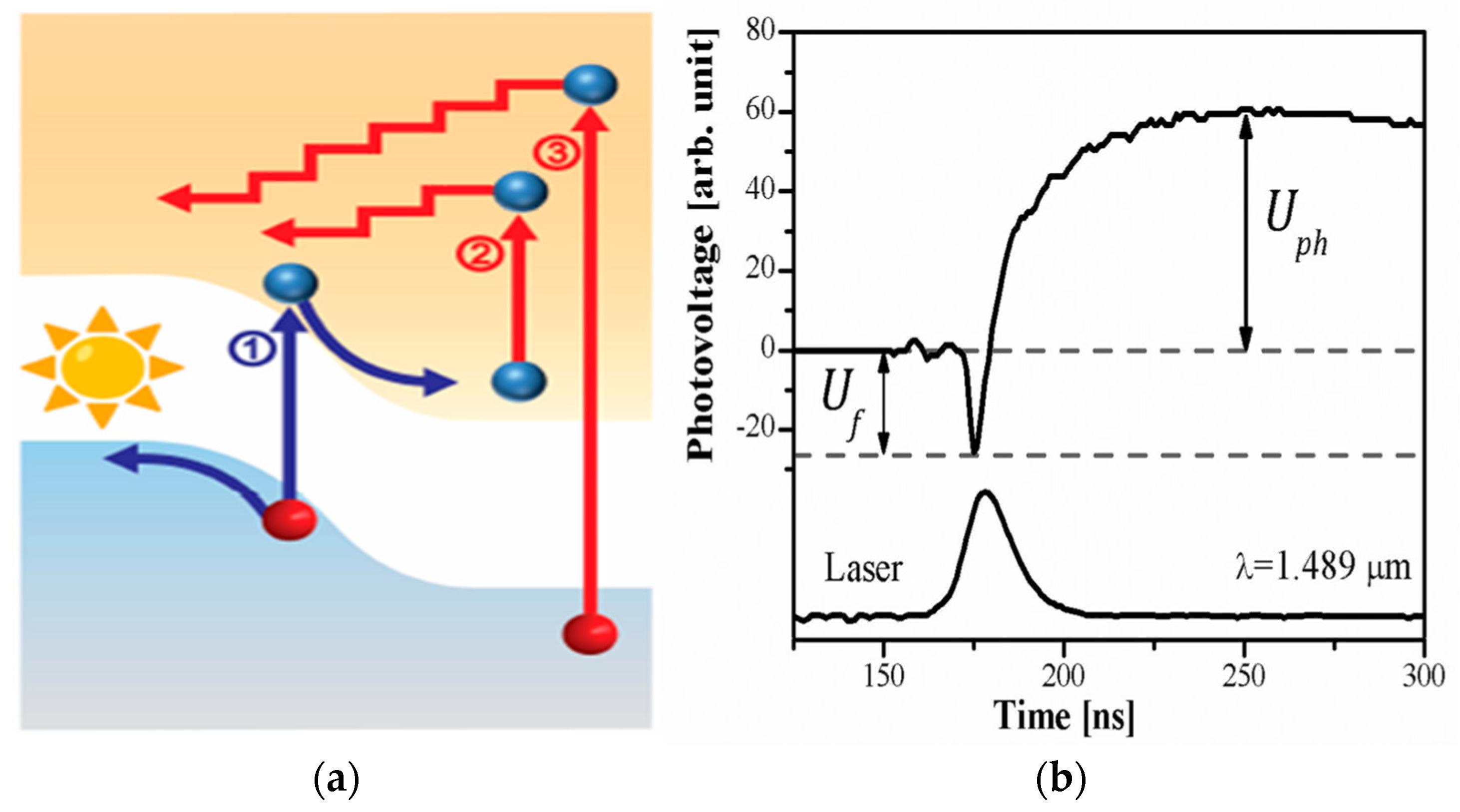
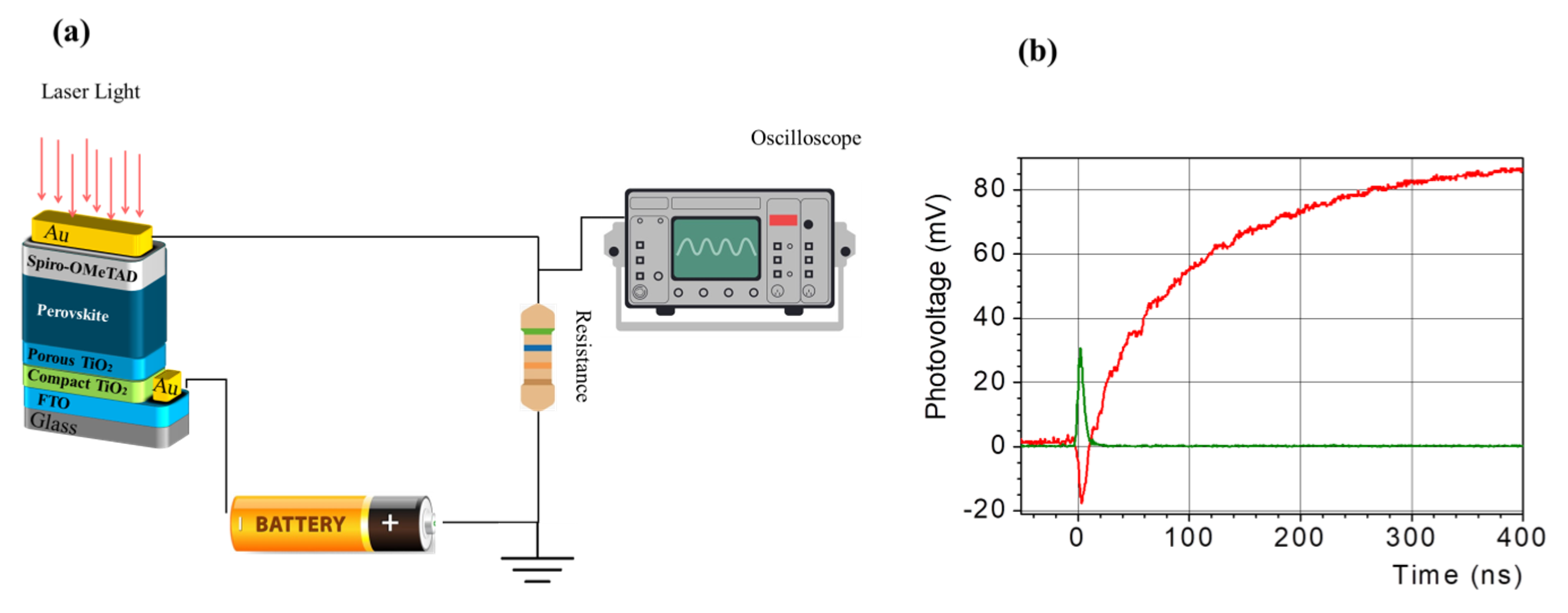
  287. Mujahid, M.; Čerškus, A.; Gradauskas, J.; Grigucevičienė, A.; Giraitis, R.; Leinartas, K.; Lučun, A.; Petrauskas, K.; Selskis, A.; Sužiedėlis, A.; et al. Unveiling the Influence of Hot Carriers on Photovoltage Formation in Perovskite Solar Cells. Materials 2025, 18, 85. [Google Scholar] [CrossRef]
  288. Hidayat, R.; Nurunnizar, A.A.; Fariz, A.; Herman; Rosa, E.S.; Shobih; Oizumi, T.; Fujii, A.; Ozaki, M. Revealing the charge carrier kinetics in perovskite solar cells affected by mesoscopic structures and defect states from simple transient photovoltage measurements. Sci. Rep. 2020, 10, 19197. [Google Scholar] [CrossRef]
  289. Ratner, M. The Physics of Solar Cells; Third Generation Photovoltaics: Advanced Solar Energy Conversion. Phys. Today 2004, 57, 71–72. [Google Scholar] [CrossRef]
  290. König, D.; Casalenuovo, K.; Takeda, Y.; Conibeer, G.; Guillemoles, J.F.; Patterson, R.; Huang, L.M.; Green, M.A. Hot carrier solar cells: Principles, materials and design. Phys. E Low-Dimens. Syst. Nanostruct. 2010, 42, 2862–2866. [Google Scholar] [CrossRef]
  291. Sherkar, T.S.; Momblona, C.; Gil-Escrig, L.; Avila, J.; Sessolo, M.; Bolink, H.J.; Koster, L.J.A. Recombination in perovskite solar cells: Significance of grain boundaries, interface traps, and defect ions. ACS Energy Lett. 2017, 2, 1214–1222. [Google Scholar] [CrossRef]
  292. Yang, S.; Fu, W.; Zhang, Z.; Chen, H.; Li, C.-Z. Recent advances in perovskite solar cells: Efficiency, stability and lead-free perovskite. J. Mater. Chem. A 2017, 5, 11462–11482. [Google Scholar] [CrossRef]
  293. Kamarudin, M.A.; Hayase, S. Passivation of Hybrid/Inorganic Perovskite Solar Cells. In Perovskite Solar Cells; Wiley-VCH: Weinheim, Germany, 2021; pp. 91–111. [Google Scholar]
  294. Ašmontas, S.; Gradauskas, J.; Grigucevičienė, A.; Leinartas, K.; Lučun, A.; Mujahid, M.; Petrauskas, K.; Selskis, A.; Sužiedėlis, A.; Šilėnas, A. Triple-cation perovskite/silicon tandem solar cell. Ukr. J. Phys. Opt. 2022, 23, 193. [Google Scholar] [CrossRef]
  295. Ašmontas, S.; Mujahid, M. Recent progress in perovskite tandem solar cells. Nanomaterials 2023, 13, 1886. [Google Scholar] [CrossRef]
Figure 1. (a) Perovskite materials, Reproduced with permission from Ref. [6], copyright 2015 Materials Today. (b) Crystallographic structure with a unit cell of cubic CH3NH3PbI3 perovskite. Reproduced with permission from Ref. [5], copyright 2015 Materials Today.
Energies 18 03543 g001
Figure 2. Calculated bandgaps at various levels of theory for (a) MAPbI3 and (b) MASnI3 perovskites. Reproduced with permission from Ref. [72], copyright 2016 ACS. (c) Schematic diagram of broadened phonon dispersion spectrum, (d) fluctuations of the orbital overlap induced by dynamic structural fluctuations. Reproduced with permission from Ref. [67], copyright 2024 Wiley.
Energies 18 03543 g002
Figure 3. (a) A photo absorber absorbs powerful photons. (b) Electrons originating from an absorber material’s VBM rapidly jump to energy levels beyond CBM (c) The particular phenomena of HC in detail (i) hot electron interaction (ii) thermalization (iii) cooling (iv) lattice temperature (d) either recombining or the charge carrier transferring to the electron-transport layer. Reproduced with permission from Ref. [1], copyright 2021 Nature.
Energies 18 03543 g003
Figure 4. The hot carrier solar cell structure is at equilibrium with the heater (Sun) and the cooler (ambient) in open-circuit conditions. Te,h is the temperature of the electron and hole gas. Blue dots represent electrons are excited by sunlight from lower energy states into higher energy states, Red dots represent holes, or the positively charged vacancies created in the valence band when electrons are excited to the conduction band. Reproduced with permission from Ref. [125], copyright 2017 Wiley.
Energies 18 03543 g004
Figure 5. (a) Schematic view of the formation of the thermoelectromotive force of HC and classical photovoltage caused by electron–hole pair generation across the p-n junction: 1—electron–hole pair generation by an equal–to-bandgap photon; 2—free electron heating; 3—generation of hot electron and hole pair. The stepped arrows indicate the cooling and diffusion of hot electrons. Analogous hot hole-related processes are omitted to avoid visual overloading. Reproduced with permission from Ref. [138], copyright 2024 MDPI. (b) Oscilloscope traces of laser pulse (bottom) and photovoltage (top) consisting of two components. Reproduced with permission from Ref. [139], copyright 2018 Sciendo.
Energies 18 03543 g005
Figure 6. Energy diagram of hot-hole and hot-electron relaxations. Reproduced with permission from Ref. [193], copyright 2019 MDPI.
Energies 18 03543 g006
Figure 7. (a) HC cooling dynamics following photoexcitation. (b) Scheme of hot electron relaxation via LO phonon emission and non-radiative Auger recombination helping to slow down hot electron cooling further. Reproduced with permission from Ref. [130], copyright 2017 Nature.
Energies 18 03543 g007
Figure 8. The hot-phonon bottleneck effect occurs because the rate of electron–phonon coupling is rapid, but the rate of phonon decay is comparatively slow. Reproduced with permission from Ref. [216], copyright 2024 ACS.
Energies 18 03543 g008
Figure 9. (a) Transient absorption spectroscopy principle: a schematic representation. (b) Groundstate bleach (dashed line), stimulated emission (dotted line), excited-state absorption (solid line), a total of these contributions shown on a ΔA spectrum (grey line). Reproduced with permission from Ref. [270], copyright 2009 Wiley.
Energies 18 03543 g009
Figure 10. (a) Scheme of the transient photovoltage measurements. Adapted with permission from Ref. [140], copyright 2024 MDPI. (b) Temporal shapes of the laser pulse (green) and photovoltage (red) of the PSC. Adapted with permission from Ref. [287], copyright 2025 MDPI.
Energies 18 03543 g010
Table 1. A comparison of HC cooling times in representative perovskites and conventional semiconductors.
MaterialCooling Time (to Near-Band-Edge Temperature)FindingRef
MAPbI3≈60 ps (high fluence, up to 600 K)Nearly two orders of magnitude slower than GaAs; lifetime reaches ≈ 60 ps at elevated carrier density[135]
CsPbBr30.8 ps (moderate density) to 17 ps (high density)Bottleneck yields 0.8 ps at ∼2 × 1018 cm−3, stretching to ∼17 ps above 1018 cm−3[131]
GaAs ≈0.6 psInferred from perovskite–GaAs comparison: perovskite is ~100× slower (MAPbI3 ∼60 ps vs. GaAs ∼0.6 ps)[1]
Si≈0.15 ps (150 fs)Thermalization via electron-phonon scattering in Si occurs in ~150 fs[133]
Table 2. Comparative analysis of HC dynamics.
Materialτcool (ps)ConditionsRef
Perovskites0.2–1 psFA/Cs/MA lead halides (varies with composition)[250]
GaAs (bulk)~1.4 psOverall cooling to CBM via Γ-valley[251]
GaAs (QWs, n > 1018 cm−3)tens–hundreds psHot-phonon bottleneck at high density[252]
Si (bulk)~0.35 ± 0.08 psProbe-wavelength TAS[253]
Si (2D phononic)10–16 psPhononic crystal suppression[254]
Disclaimer/Publisher’s Note: The statements, opinions and data contained in all publications are solely those of the individual author(s) and contributor(s) and not of MDPI and/or the editor(s). MDPI and/or the editor(s) disclaim responsibility for any injury to people or property resulting from any ideas, methods, instructions or products referred to in the content.

