Article

A Coordinated Communication and Power Management Strategy for DC Converters in Renewable Energy Systems

1
Department of Electronics and Informatics, Gunma University, Kiryu 376-8515, Gunma, Japan
2
Yangzhou Polytechnic Institute, Yangzhou 225127, China
*
Author to whom correspondence should be addressed.
Energies 2025, 18(13), 3329; https://doi.org/10.3390/en18133329
Submission received: 8 May 2025 / Revised: 10 June 2025 / Accepted: 20 June 2025 / Published: 25 June 2025

Abstract

Effective communication among distributed energy sources (DESs) is essential for optimizing energy allocation across power sources, loads, and storage devices in integrated renewable energy and energy management systems. This paper proposes a novel communication and energy management strategy to address challenges related to communication interference and inefficiencies in energy management. The proposed strategy employs the DC bus as a communication medium, enabling module coordination via pulsed voltage signals. Controller modules regulate the bus voltage based on the energy state of the bus and control the supplementary or absorptive energy flow from slave modules to maintain voltage stability. Simultaneously, communication between the master and slave modules is achieved through pulsed voltage signals of varying pulse widths, and power sharing is realized via droop control. Experimental results demonstrate that the proposed method effectively distributes energy across different voltage levels, enabling the controller modules to precisely regulate the voltage of the slave modules under varying load conditions.

1. Introduction

Renewable energy integration and management systems are critical components of modern energy systems. Using technology, they integrate distributed renewable energy sources, such as solar and wind energy, into the grid. This facilitates efficient energy utilization and collaborative operation, leading to the development of stable and efficient DC microgrids [1]. These systems offer significant advantages for both power companies and users. They can supplement the primary grid, flexibly adjust the load, and meet real-time transmission and distribution demands [2]. Additionally, they can cater to users’ specific power quality requirements. The flexibility, scalability, and energy exchange capabilities of microgrids with the primary grid have made them a key research focus in the energy sector [3].
Regarding DC–microgrid control strategies, two common approaches are employed: one relies on external communication, and the other does not. In communication-dependent systems, stability is vulnerable to communication failures. However, communication-independent methods are limited by the number of distributed energy sources and may require additional complex circuitry, which can interfere with communication signals [4]. This paper proposes a pulse communication method based on bus voltage to address these challenges. This approach aims to improve microgrid stability, effectively manage distributed energy sources, and provide a novel solution for addressing microgrid control challenges [5].

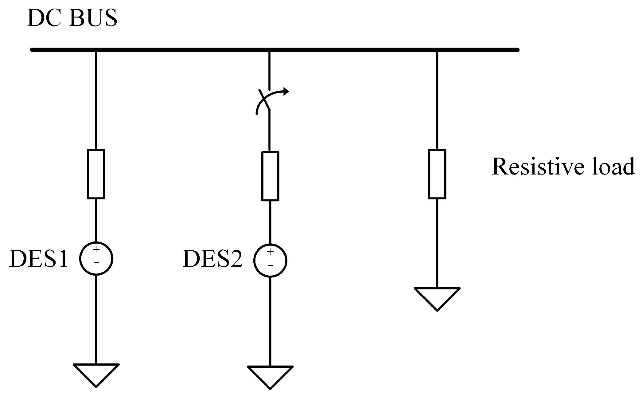
2. Analysis of Pulse Signal Method Based on Bus Voltage

The efficient coordination of distributed energy storage systems (DESs) is critical for promoting DC microgrid technology. This paper proposes a pulse signal control strategy based on bus voltage to enhance DES’s operational efficiency. The approach is based on a differential evolution strategy, incorporating a distributed management mechanism to promote effective collaboration between DESs [6].
The control strategy adopts a master–slave control architecture. The master control module monitors the DC bus voltage, manages the energy balance, and ensures an accurate supply. The slave control module operates in the current mode, delivering the required energy to the microgrid [7,8]. The bus voltage is the key to coordinating the master–slave modules. The controller and agent modules automatically perform the corresponding control actions based on changes in bus voltage. This response mechanism, driven by bus voltage variations, supports the stable and efficient operation of the microgrid [9,10].
This innovative control method is expected to significantly improve the efficiency of energy management and system stability of DC microgrids.

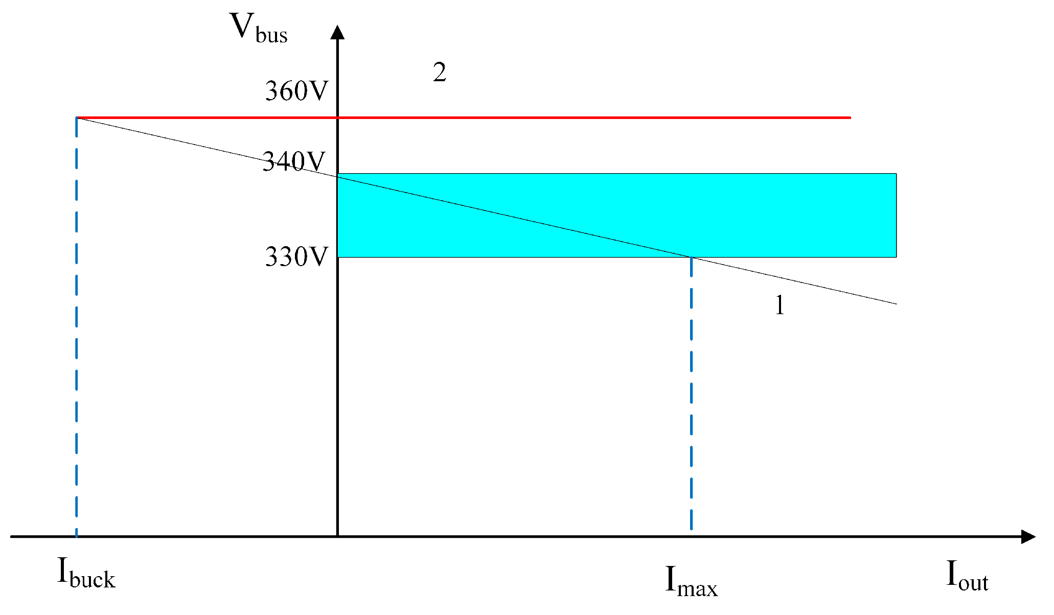
2.1. Droop Curve Analysis

In the control strategy proposed in this paper, the system involves only two distributed energy units during each information exchange: a controller module and an agent module, with their connecting circuit shown in Figure 1. Other modules must wait for the current agent module to complete the information exchange before starting their communication process [11,12].
When the slave module is connected to the DC bus for communication, it is assumed that the two distributed energy systems (DESs) involved in the information exchange each have a droop curve, as expressed by Equation (1). Here, V ref represents the preset value in voltage mode, V out k is the actual output voltage in voltage mode, and I out k is the output current. R vir k is the virtual resistance set in the controller, which determines the slope of the droop control curve [13].
V out k = V ref k I out k · R vir k , k { 1 , 2 } .
If two DES converters are operating in parallel, their output voltages V out 1 and V out 2 will be equal. Based on this condition, we can derive Equation (2).
I out 1 = V ref 1 V ref 2 R vir 1 + R vir 2 · I out 2 R vir 1 , ( R vir 1 0 ) .
When the system is connected to a distributed energy storage system (DES), the voltage–current curves for the main module DES1 and the slave module DES2 can be derived from the two formulas above, as shown in Figure 2, where number 1 represents the preset value V ref 1 in the voltage mode, and number 2 represents the preset value V ref 2 [14,15].
Figure 2a illustrates the curve relationship between the two energy modules, with the voltage–current relationship described by Equation (2). Upon analyzing Figure 2a, it is observed that there is no clear correlation between DES2 and the DC bus voltage when DES2 is connected or disconnected. Therefore, this relationship curve is not suitable for system analysis and application.
Figure 2b presents the droop curve commonly referenced in most literature, where both modules share the same reference voltage V ref . The figure shows that the current distribution between the two modules can be derived from Equation (3).
I out 1 = R vir 2 · I out 2 R vir 1
When DES2 is connected to the DC bus, part of the load current is supplied by DES2, leading to a gradual increase in the bus voltage. However, this voltage variation is unsuitable for bus voltage signal exchange because the voltage level is not fixed. The connection of different energy sources to the system results in varying voltage levels, and load fluctuations further contribute to bus voltage instability. These variations can lead to system malfunctions. Therefore, such droop curves are not suitable for system control. Similarly, although the droop curves shown in Figure 2c are identical, they are also inappropriate for system control.
In Figure 2d,e, one module has a droop coefficient of zero, leading to different quadrant positions for the intersection points of the two curves. In Figure 2d, the main module operates with a droop coefficient, whereas the slave module has a droop coefficient of zero. When DES2 is connected, the bus voltage decreases to V ref 2 .
Under these conditions, the output current of DES1 remains constant at I out 1 , while the current supplied by DES2 is determined by the load demand. Similarly, in Figure 2e, when DES2 is connected, the bus voltage increases to V ref 2 .
Theoretically, both configurations shown in Figure 2d,e can be employed for control. However, in Figure 2d, the current of DES2 becomes uncontrollable once it is connected. If the load demand is low, DES2 could generate excessive current, which may lead to undesirable effects. This configuration is only viable if DES2 is a bidirectional energy storage device capable of handling both positive and negative currents, such as a battery or supercapacitor. In contrast, this configuration is unsuitable for unidirectional energy sources, such as photovoltaic systems.
In Figure 2e, when DES2 is connected, the current of DES1 remains constant and negative, while DES2 supplies a constant and positive current.
This paper proposes a DC bus voltage pulse signal method. During system operation, droop control voltage is used, while a voltage level higher than the droop control voltage is applied for communication [16,17]. The specific operating and communication voltage levels are shown in Figure 3.
As shown in the figure, the blue area and the slash 1 intuitively present the working characteristics of the master module affected by the droop coefficient, with its actual voltage fluctuating between 330 V and 340 V and following the droop control law with the change of output current, which is consistent with the voltage setpoint of 340 V for the master module in the controller and the actual working voltage range affected by the droop coefficient. The red horizontal line 2 represents the communication voltage level of 360 V, which is higher than the droop control voltage and is specially used for system communication. It is worth noting that if a slave module is connected and the master module does not limit the current, an uncontrollable reverse current may be generated in the actual circuit, which may lead to system instability.
To prevent this issue, the current limits of the inner current loop in the master module controller are set between 0 and I max . This ensures that when the slave module is connected, the master module operates with zero current, effectively remaining inactive, while the bus load determines the current of the slave module. This approach prevents reverse current in the master module, thereby avoiding potential system instability.

2.2. Analysis of Communication Method

Traditional droop control methods typically employ the same floating voltage and droop coefficient [18]. In contrast, this paper introduces a novel droop control strategy based on a pulse signal method, which leverages the DC bus voltage. This approach facilitates communication by adjusting the bus voltage, eliminating the need for additional circuits or devices [19]. By regulating the bus voltage, it coordinates the operation of distributed energy sources, ensuring the efficient and orderly functioning of the DC microgrid system [20].
During system operation, the nominal bus voltage is set to 340 V and is initially controlled by the master module. Upon connection of a slave module, it assumes control of the bus voltage, raising it to 360 V to facilitate communication. At this point, the master module detects changes in the bus voltage to identify the presence of a slave module. Once communication is completed, the slave module ceases its operation, and control of the bus voltage is returned to the master module, resuming normal operation. The system differentiates between slave modules by assigning distinct time intervals for each to control the bus voltage.
When slave module 1 connects to the system, it raises the bus voltage to 360 V and maintains this voltage for a duration of t 1 . After t 1 , slave module 1 enters a sleep state, and control of the bus voltage is returned to the master module. During system operation, slave modules briefly operate in voltage mode upon connection for communication.
The operation of slave module 2 is similar to that of slave module 1, with the key difference being the communication duration; slave module 2 maintains the 360 V voltage for t 2 , allowing the system to distinguish between the two slave modules. While a slave module controls the bus voltage, the master module identifies which slave module is currently connected by monitoring the duration of the 360 V voltage level.
When the system load increases, the slave modules are required to supply power to the bus, thereby alleviating the burden on the master module. In this scenario, the master module raises the bus voltage to 360 V as a communication signal. To activate slave module 1, the master module sends the connection signal specific to slave module 1; to activate slave module 2, the corresponding signal for slave module 2 is sent. Similarly, when the bus load decreases and a slave module needs to be disconnected, the master module issues the appropriate signal. This communication mechanism is illustrated in Figure 4. If additional slave modules are integrated into the system, they can be distinguished by adjusting the duration of the communication voltage.
The key distinction of this communication method is based on time allocation. In this paper, the communication time t 1 is set to 1 s, while t 2 is set to 2 s. Different time combinations are used as communication signals, as shown in Figure 5. The advantage of this communication method lies in its ability to quickly identify different slave modules while theoretically supporting unlimited expansion.

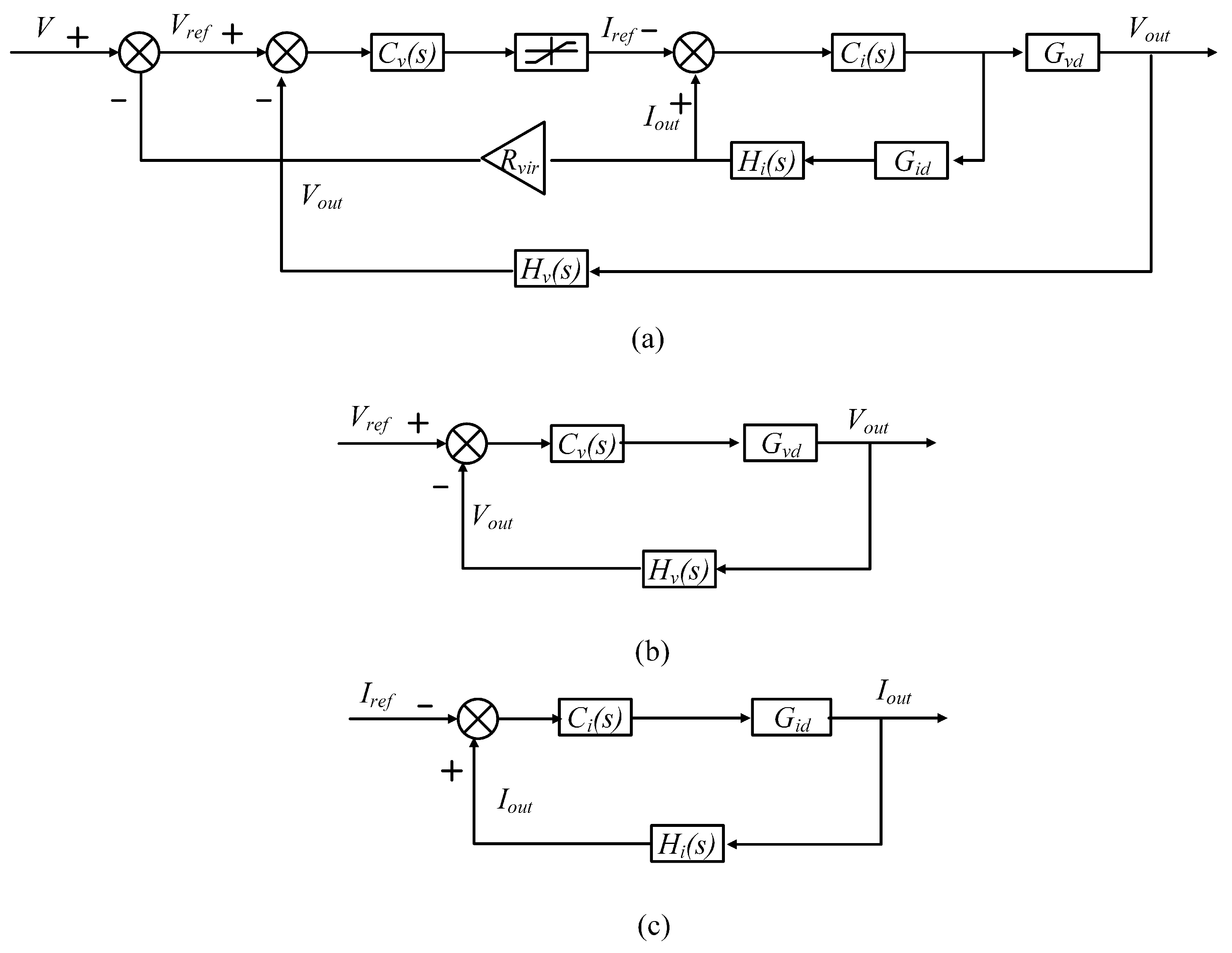
3. Controller Design

The core mechanism of the pulse signal method, based on the DC bus voltage proposed in this paper, is as follows: During system operation, the master module is responsible for controlling the bus voltage, ensuring stable operation within the droop control range [21,22]. When communication with the slave module is required, the slave module raises the bus voltage to 360 V, which serves as the communication voltage level with the master module. If the system load increases, the master module raises the bus voltage to the preset communication voltage level, activating the slave module to support the bus. During this process, the slave module operates in constant current mode, supplying power to the bus.
In the overall system architecture, the master module has two control modes: the voltage closed-loop control mode and the voltage–current dual-loop control mode with a droop curve. The slave module also has two control modes: the voltage closed-loop control mode and the current closed-loop control mode. The control block diagram in Figure 6 presents the specific control architecture.
In Figure 6, Figure 6a illustrates the voltage–current dual-loop control mode with a droop curve. This mode employs a classic dual-loop control strategy with an inner current loop and an outer voltage loop. The virtual resistance value R v i r set in the controller plays a decisive role in shaping the droop curve. By adjusting the value of R v i r , the droop characteristics of the system can be flexibly adjusted to suit different operating conditions.
Figure 6b presents the voltage closed-loop control mode. This mode’s primary function is to maintain the bus voltage at a constant level, ensuring the stability of the system’s supply voltage and providing a stable operating voltage environment for various load devices.
Figure 6c presents the current closed-loop control mode. This mode is primarily used to control the slave module, enabling it to either supply power to the DC bus with a constant current or absorb power from it. This ensures the precise regulation of the system’s power flow, contributing to its efficient and stable operation under varying load conditions.
In the control system, V r e f represents the set reference voltage value, and I r e f represents the set reference current value. The actual output voltage is V o u t , and the actual output current is I o u t . C v ( S ) is the transfer function of the voltage controller, and C i ( S ) is the transfer function of the current controller. G v d ( S ) describes the relationship between the output voltage and duty cycle, while G i d ( S ) describes the relationship between the output current and duty cycle. H v ( S ) and H i ( S ) are the transfer functions of the voltage and current sensors, respectively.
For the voltage outer-loop PI controller shown in Figure 6a, the computed value is limited and used as the reference for the current inner-loop controller. The limitation is applied to define the circuit’s maximum and minimum current values, ensuring stable operation.
As shown in Figure 6a, V r e f is obtained by subtracting the product of the output current and the virtual resistance R v i r from V, which is the key to droop control. When R v i r and V remain constant, as the output current increases, the value of V r e f decreases, causing V o u t to decrease as the output current increases. From the voltage–current curve in Figure 2, it can be seen that R v i r determines the slope of the current working curve of the controller.

4. System Operating Mode Analysis

In the system proposed in this paper, the master module has three operating modes, while the slave module has seven operating modes. Therefore, analyzing the different operating modes of the master and slave modules and the logical relationships between these modes is of significant importance for the design of the control program [23,24,25].

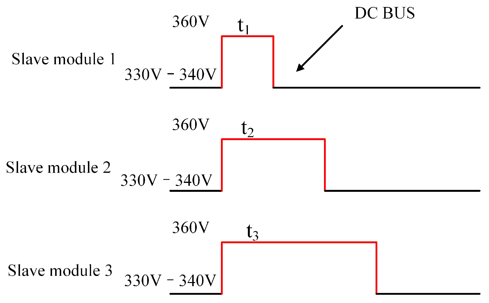
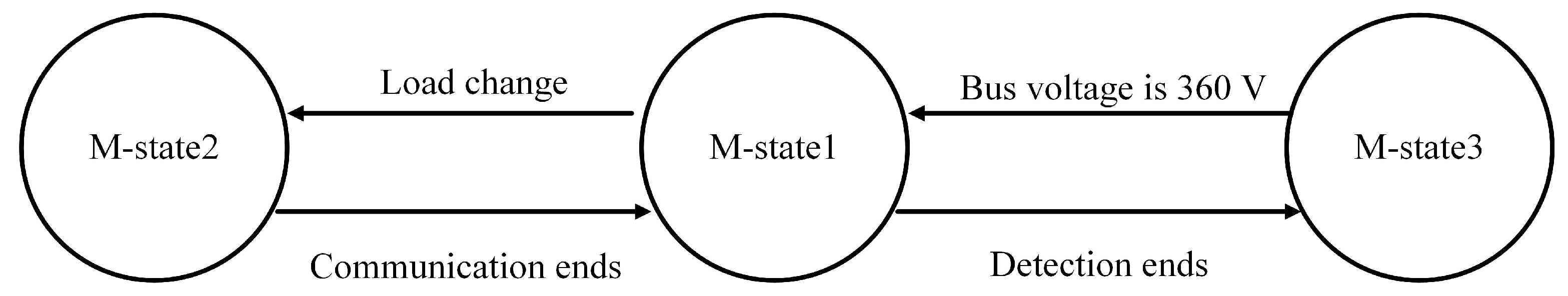
4.1. Master Module Operating Mode Analysis

In the system design, the master module has the following three operating modes, and their logical relationships are shown in Figure 7.
I. M-state 1: The master module controls the bus voltage between 330 V and 340 V. When the load changes, the system switches to M-state 2. If the slave module controls the bus voltage to 360 V, the system enters M-state 3.
II. M-state 2: In this mode, if the load decreases, the master module maintains the current operating mode. When the system load increases, the master module controls the bus voltage. It sends a communication signal to wake up the connected slave module to provide additional power to the bus. If the load decreases, the master module controls the bus voltage and sends a communication signal to disconnect the slave module, providing power to the bus, and then returns to M-state 1.
III. M-state 3: In this mode, the master module monitors the bus voltage, analyzes the received signals, and marks the status of the slave module in the controller before returning to M-state1.
These modes’ proper switching and control are crucial for ensuring that the system operates stably and communicates effectively.

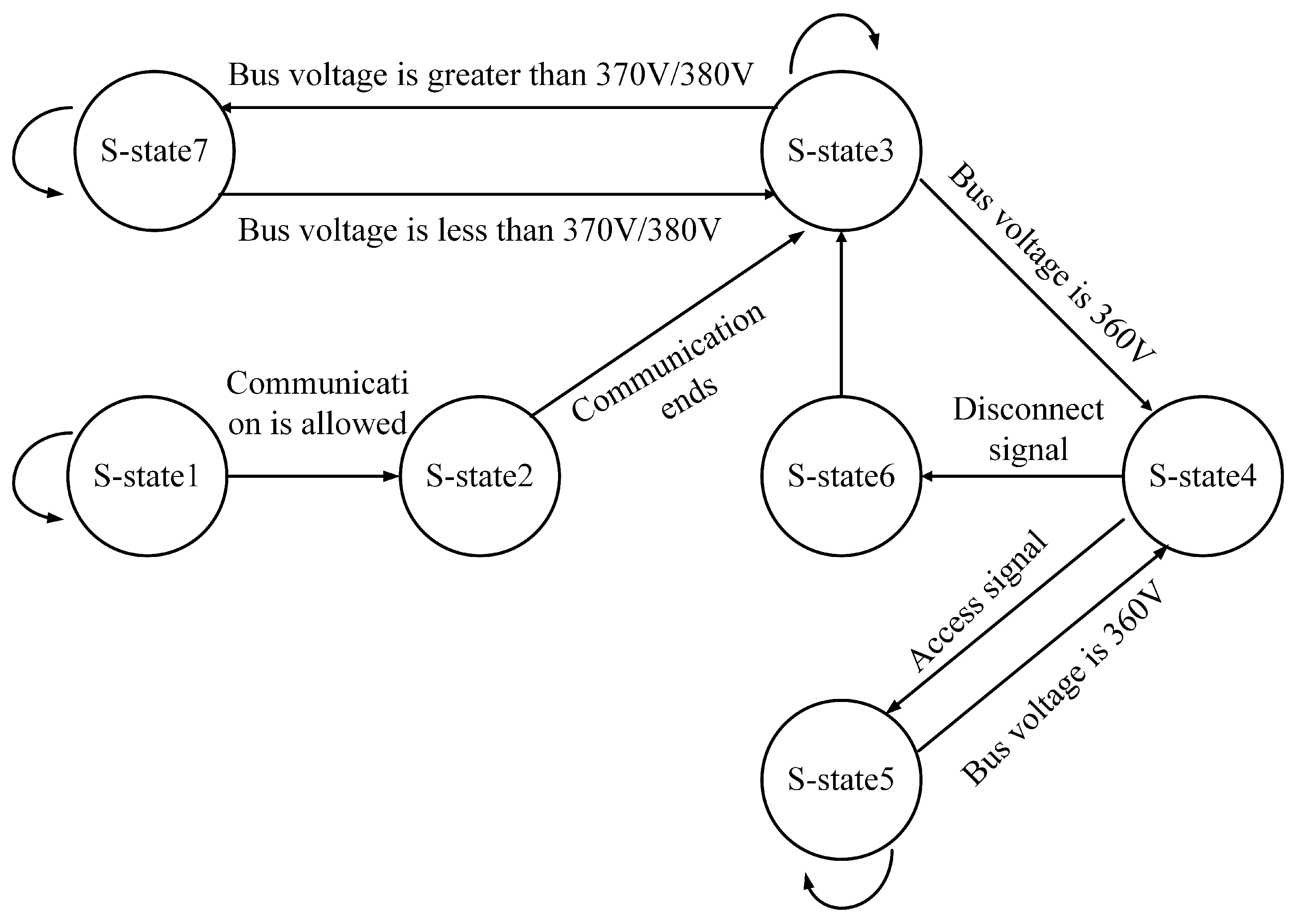
4.2. Slave Module Operating Mode Analysis

The slave module operates in seven modes, with their logical relationships shown in Figure 8:
I. S-state 1: The slave module waits for the external switch to connect to the DC microgrid. Once connected, if another slave module does not control the bus voltage, it enters S-state 2; if controlled, it waits until the control ends.
II. S-state 2: The slave module raises the bus voltage to 360 V for communication. After communication ends, it enters S-state 3.
III. S-state 3: The slave module enters sleep mode while continuously monitoring the bus voltage for any wake-up signal from the master module. If a signal is detected, it enters S-state 4.
IV. S-state 4: The slave module receives and analyzes the signal. If it is a wake-up signal for the module, it enters S-state 5; if it is a power absorption signal, it enters S-state 7.
V. S-state 5: The slave module is awakened, starts providing power to the bus, and continuously monitors signals from the master module. If a disconnect signal is received, it enters S-state 6.
VI. S-state 6: The slave module receives and analyzes the signal. If it is a disconnect signal for the module, it enters sleep mode and returns to S-state 3.
VII. S-state 7: The slave module operates in reverse constant current control mode, absorbing power from the bus. If the bus voltage falls below the set threshold, it returns to S-state 3.
These modes ensure that the slave module can flexibly respond to commands from the master module while entering an energy-saving sleep mode when not needed.

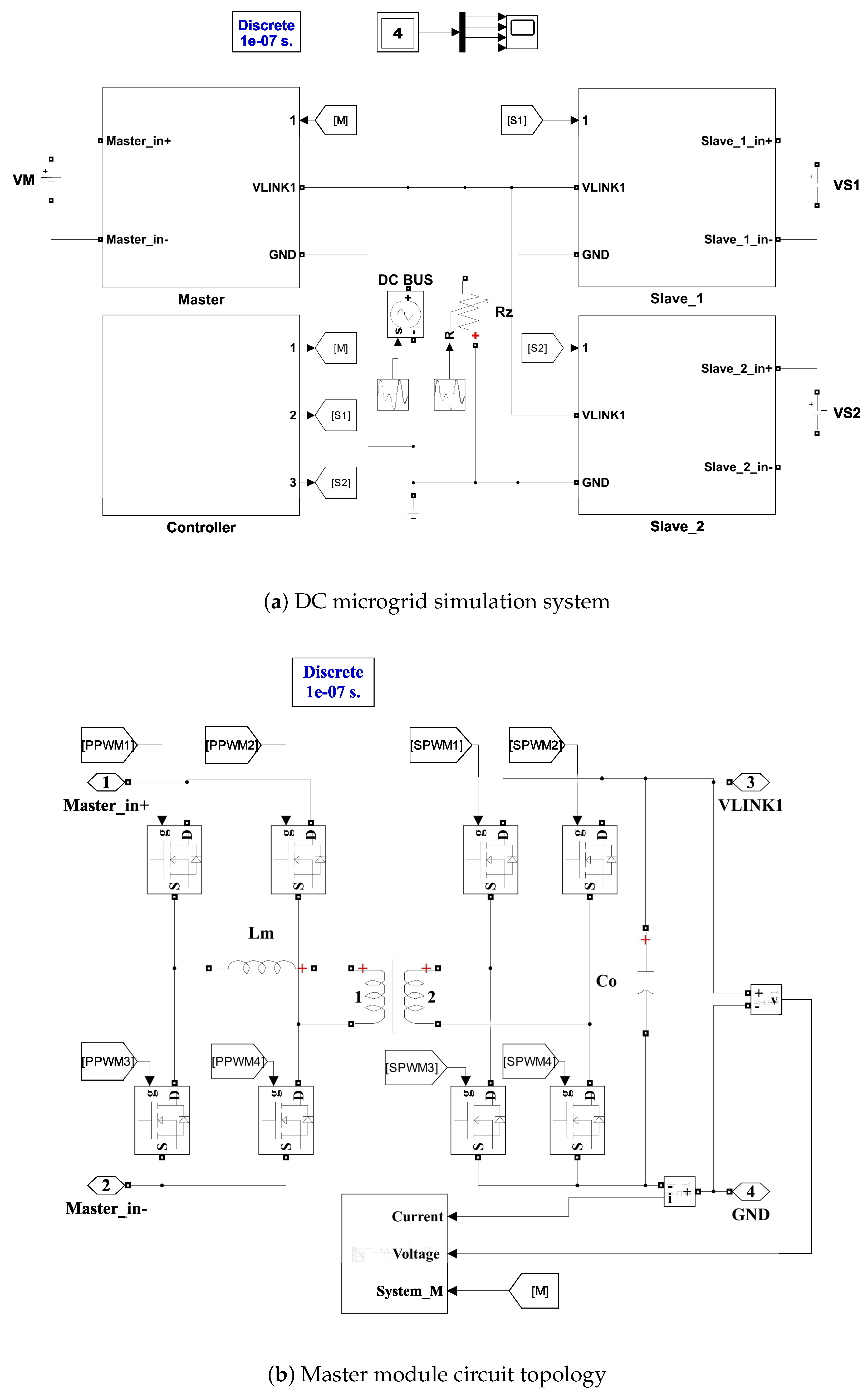
5. Simulation Verification

To validate the effectiveness of the pulse signal method based on DC bus voltage proposed in this study, a DC microgrid simulation system was developed, comprising a master module, two slave modules, and a variable load. Each module adopts a four-quadrant DC–DC converter topology. The input of the master module is connected to a regulated DC power supply, while the slave modules are powered by batteries. The overall simulation system is illustrated in Figure 9a, the detailed module circuit is presented in Figure 9b, and the corresponding circuit parameters are listed in Table 1. Based on this simulation platform, the communication capabilities of the proposed method are evaluated under four conditions: fixed load, variable load, bus voltage variation, and constant power load.

5.1. Simulation Verification of Fixed Load

To verify the communication principle analyzed in Section 3, the communication function between the master module and two slave modules in a fixed load mode is simulated and verified. The bus load resistance is selected as 68 ohms, and the simulation results are shown in Figure 10.
As illustrated in the simulation waveform of Figure 10a, upon the connection of slave module 1, the DC bus voltage is elevated to 360 V under its regulation, indicating that the bus load should be entirely supplied by slave module 1. However, the waveform reveals that during the initial second, as the bus voltage ramps up to 360 V, the master module still delivers a current of 0.3 A, while the output current of slave module 1 surges to 5 A. Following the issuance of a wake-up signal by the master module, slave module 1 promptly responds and transitions to current control mode to supply power to the bus. During this phase, slave module 1 operates in a cross-current control mode, maintaining a constant output current of 2 A, whereas the master module’s output current decreases to 3 A. Once the master module transmits the cut-off signal, slave module 1 reverts to sleep mode and remains on standby until the next wake-up signal is received.
The simulation waveform in Figure 10b illustrates the operating behavior of slave module 2. Compared with slave module 1, slave module 2 initiates communication at 2 s. Apart from the timing difference, the remaining operational process remains identical.

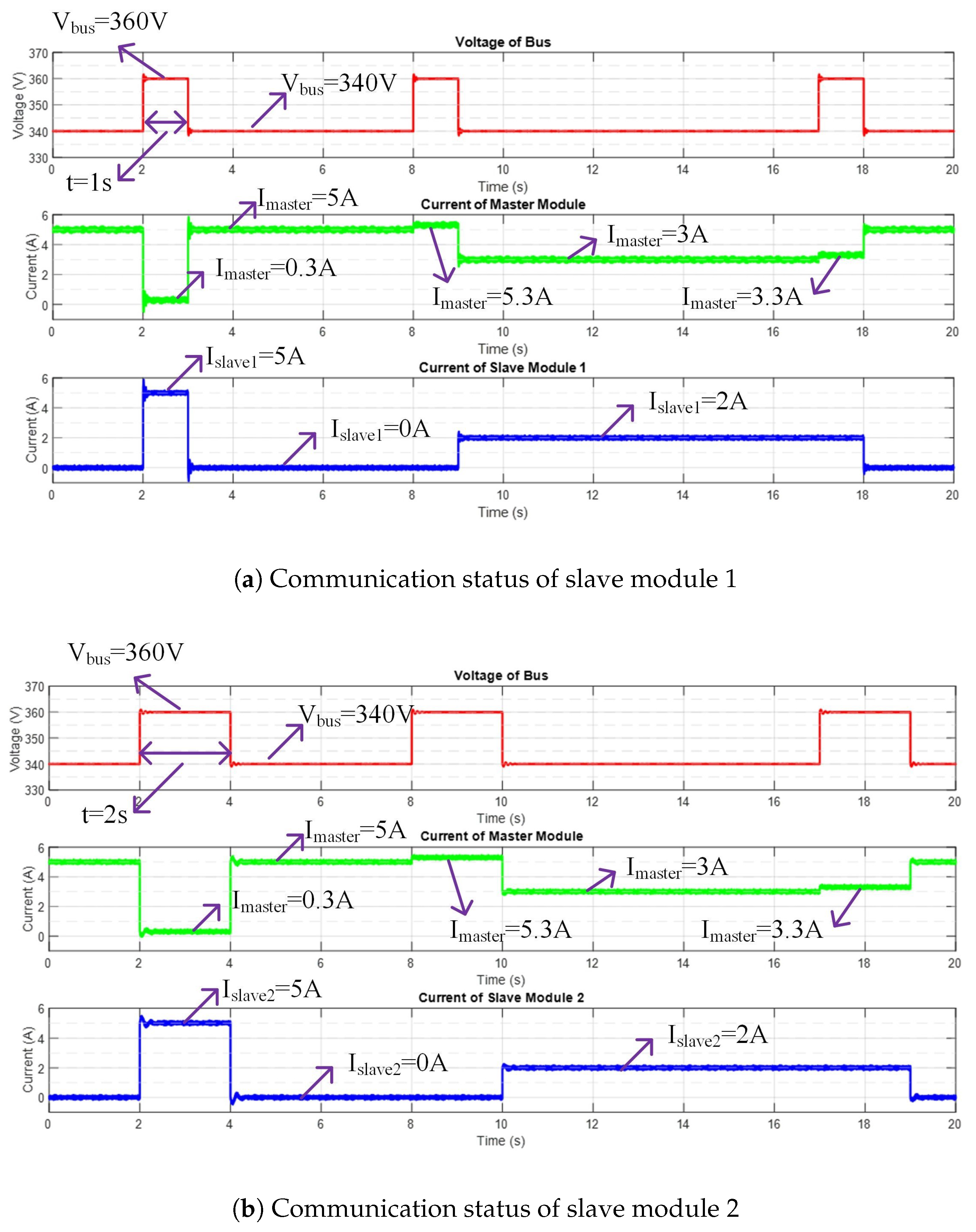
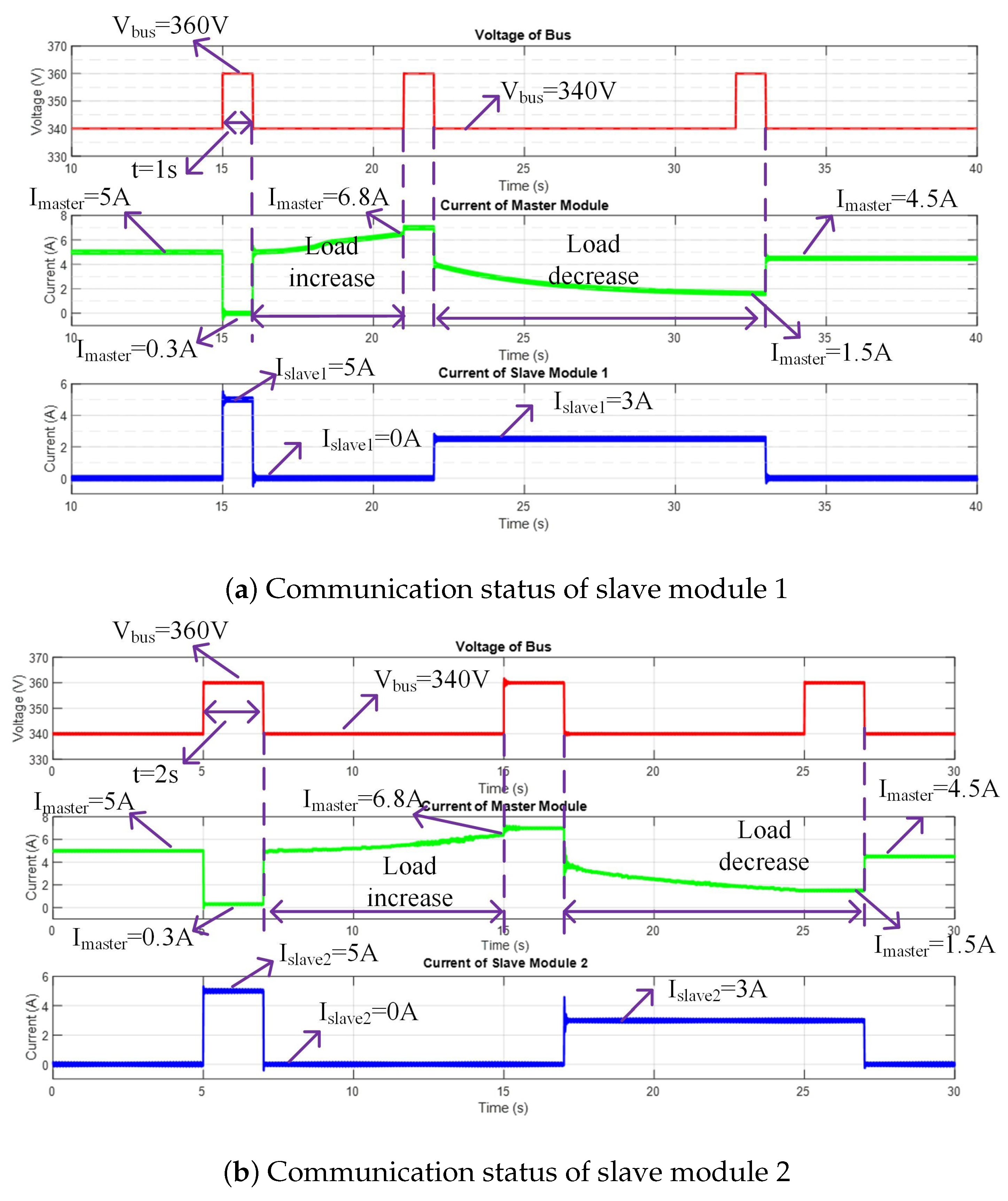
5.2. Simulation Verification of Load Variation

In practical application scenarios, the load of a DC microgrid is time-varying. To evaluate the applicability of the DC bus voltage pulse signal method proposed in this paper, a load variation simulation was conducted. In this simulation, the load first increases and then decreases, exhibiting a continuous variation trend, with the load resistance ranging from 50 to 75 Ω . The corresponding simulation results are presented in Figure 11.
As shown in Figure 11a, when the bus load increases and the output current of the master module exceeds the predefined upper limit of 6.8 A, the master module initiates a communication signal to activate the slave module for bus power support. Upon receiving the signal, the slave module responds by supplying a constant current of 3 A. When the current output of the master module drops below the predefined 4.5 A, another communication signal is sent by the master module to deactivate the slave module. In response, the slave module ceases operation and enters a sleep mode, awaiting the next activation command.
The simulation waveform in Figure 11b illustrates the operating process of slave module 2. Compared with slave module 1, the communication activation time for slave module 2 is 2 s, while all other aspects remain consistent.

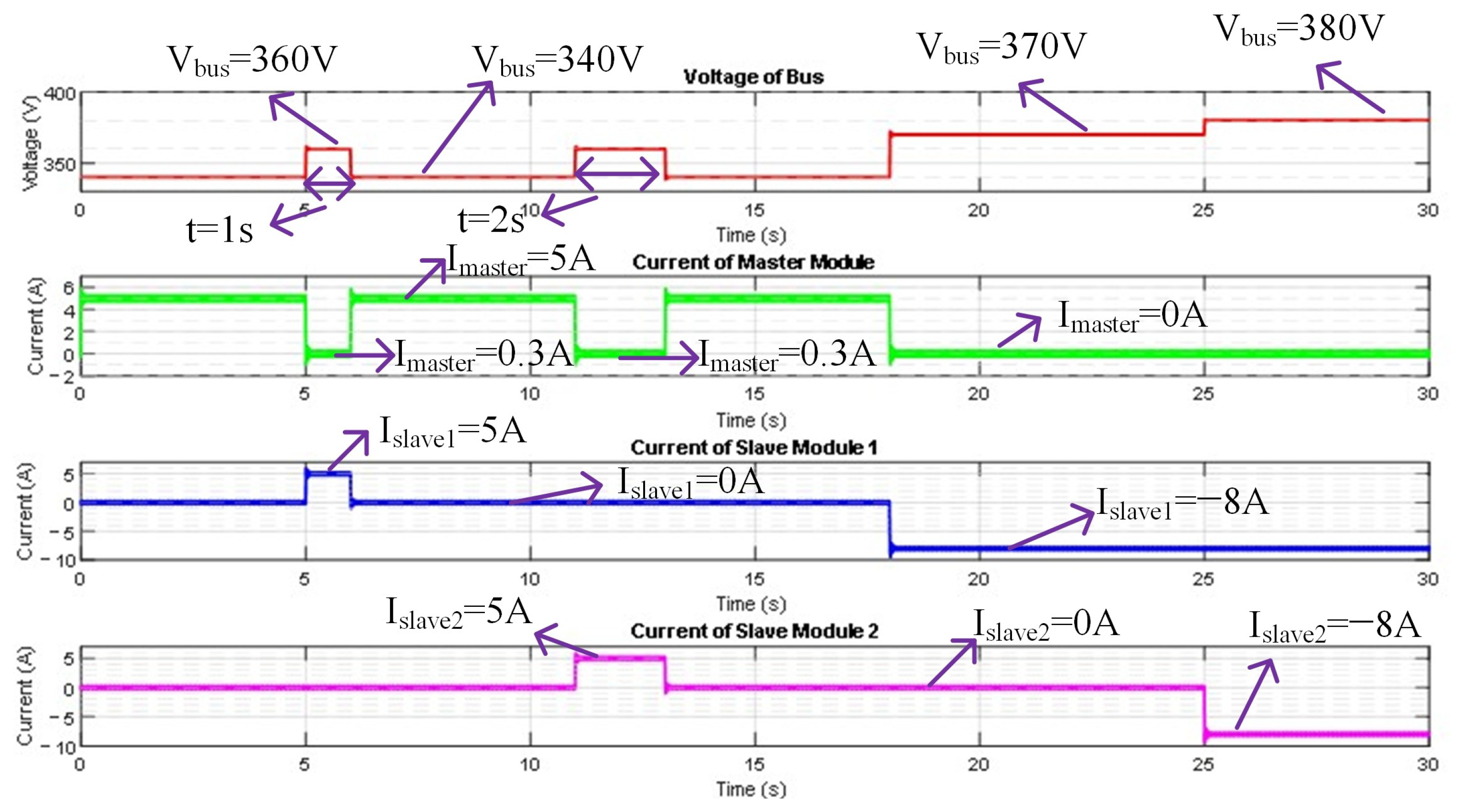
5.3. Simulation Verification of Bus Voltage Change

The circuit topology used by the master–slave module can transmit power in both directions. The previous section has verified that the slave module can provide power to the bus. When the bus voltage is too high, the slave module needs to absorb part of the bus power in time to control the bus voltage within a reasonable range to ensure the safety and reliability of the system.
We simulated the system operation status when the bus voltage changes, and the results are shown in Figure 12. The bus voltage threshold is set to wake up the slave module to absorb energy. In this simulation, the bus voltage value responded by slave module 1 is set to 370 V, and the bus voltage value responded by slave module 2 is set to 380 V.
As illustrated in Figure 12, when the bus voltage exceeds 370 V, slave module 1 autonomously wakes up and draws 8 A of current from the bus to charge battery VS1. As the bus voltage further rises to 380 V, slave module 2 is similarly activated and absorbs 8 A of current from the bus to charge battery VS2.

5.4. Simulation Verification of Constant Power Load

The verification of constant power load is not only an important part of the theoretical research of DC microgrids but also a key link to achieving safe and stable operation and efficient control of microgrids. Therefore, this paper verifies the proposed communication strategy under constant power load. The simulation model and results are shown in Figure 13.
Because the core of the proposed communication strategy is to regulate the bus voltage to facilitate direct communication between the master and slave modules, validation under constant power load conditions is carried out with the bus voltage held fixed. A simulation model, depicted in Figure 13a, was developed wherein the constant power load is realized using a controlled current source in parallel with a resistive load.
As shown in Figure 13b, before 10 s, the system maintains a power level of 1700 W. After slave module 1 is activated and integrated into the system, and the load is jointly supplied by the master module and slave module 1. During this period, the bus voltage remains at 340 V, with the master module delivering 3 A and slave module 1 supplying 2 A. At 10 s, when the load power is increased to a constant 2720 W, the bus voltage is still regulated at 340 V. The system continues to be powered cooperatively, with the master module current increasing to 4 A and the current from slave module 1 rising to 4 A. Between 11 s and 13 s, the awakening of slave module 2 for communication purposes causes the bus voltage to increase to 360 V, during which the master module output current stabilizes at 3.5 A. Upon the integration of slave module 2 at 13 s, the master module current decreases to 2 A, and slave module 2 begins supplying 2 A. Subsequently, at 16 s, the load power is adjusted again to 2040 W. The figure illustrates that slave module 1 responds swiftly, regulating its output current to 2 A.
These simulation results, as presented in Figure 13b, confirm the effectiveness of the proposed communication strategy under constant power load conditions.

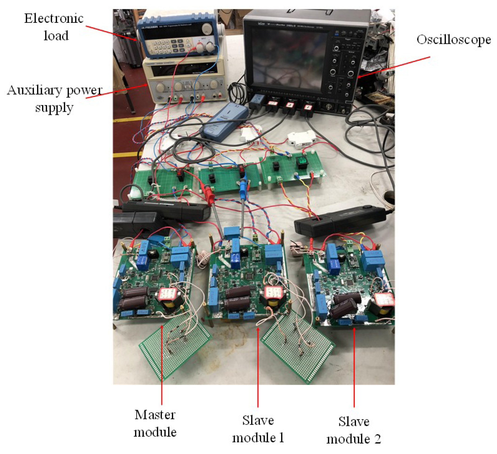
6. Experimental Verification

The experimental platform is constructed as shown in Figure 14. Three converters are used in the system to realize the functions of the master module, slave module 1, and slave module 2, respectively. The circuit parameters are the same as the simulation parameters in Section 4. Among them, the input voltage of the master module is provided by a DC regulated voltage, the two slave module inputs are connected to two 24 V batteries, and the bus voltage works at 30 V. Considering the safety of the experiment and the voltage limit of the existing laboratory equipment, a low-voltage power supply is used to simulate the system behavior without losing the versatility for high-voltage applications. Because the experimental circuit parameters are designed according to high-power scenarios and the voltage level used in the actual experiment is lower, the working state of the circuit components deviates from the design expectations, which in turn causes harmonics to appear in the experimental waveform.

6.1. Experiment of Fixed Load

Before the load change experiment, a preliminary experiment was conducted to verify the communication and coordination mechanism between the master and slave modules. Specifically, the experiment aims to confirm whether the master module can accurately detect the presence of the slave module and whether the slave module can correctly respond to the connection and disconnection commands from the master module under a fixed control signal. In the experiment, the communication voltage is selected as 31 V, and the load resistance is selected as 12 Ω . The corresponding experimental waveform is shown in Figure 15.
As shown in Figure 15a,b, the slave module can accurately respond to the wake-up and disconnection signals of the master module and smoothly switch its working mode. This proves the responsiveness of the slave module and the effectiveness of the system control strategy.

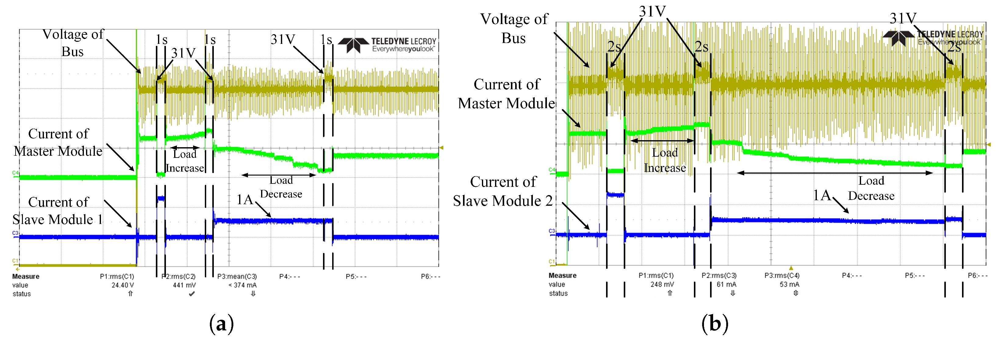
6.2. Experiment of Variable Load

To evaluate the response of the master–slave modules to load variations under realistic operating conditions, an electronic load was introduced into the experimental setup to emulate a resistive load connected to the DC bus. The resistance value was dynamically adjusted in real time to induce variations in the load. During the experiment, the load resistance was varied within the range of 10 to 20 Ω . The corresponding experimental waveforms are shown in Figure 16.
Figure 16a,b show that when the busload increases and causes the current of the controller module to exceed the set upper limit value of 3 A, the controller module will send a communication signal to request the agent module to supply power to the bus. Once the communication signal ends, the agent module immediately responds and stably outputs a current of 1 A.
In contrast, when the controller module’s current drops below the set lower limit value of 1.5 A, it sends a signal to disconnect the agent module. After receiving this signal, the agent module stops working and enters the sleep state, waiting to be woken up next time. This enables automatic connections and disconnects to meet the demands of load changes.

6.3. Experiment on Bus Voltage Variation

The system’s agent modules’ functions are not limited to providing energy to the DC bus when the bus load increases. They also include storing energy in the DC microgrid. When energy accumulation on the DC bus causes the voltage to rise, agent modules need to be able to absorb this energy promptly to maintain the bus voltage within the normal range and prevent damage to the system’s power devices.
In this experiment, it is set that agent module 1 will respond when the bus voltage reaches 32 V, while agent module 2 will respond when the bus voltage reaches 33 V. The relevant waveforms of the experiment are shown in Figure 17.
As illustrated in Figure 17, when the bus voltage exceeds 32 V, slave module 1 is automatically awakened and begins to draw power from the bus at a current of 4 A to charge the battery connected to its input. Subsequently, upon the bus voltage reaching 33 V, slave module 2 is similarly awakened and starts to absorb power from the bus at a current of 4 A to charge its corresponding input-side battery.

7. Conclusions

This paper proposes an innovative method to enhance the energy management efficiency of DC microgrids by utilizing DC bus voltage pulse signals. The proposed approach allows the master module to accurately identify and flexibly control slave modules by assigning a unique communication voltage to each slave, thereby accommodating varying load characteristics on the DC bus.
Simulation and experimental results from a DC microgrid system composed of master and slave modules confirm that the proposed method effectively enables power management under fixed resistance, variable resistance, and constant power load conditions. Furthermore, it is demonstrated that this method improves energy distribution capabilities in response to fluctuations in DC bus voltage, thereby enhancing the overall controllability and stability of the system.

Author Contributions

Conceptualization, F.Z. and T.K.; Methodology, F.Z. and W.J.; Software, F.Z.; Validation, F.Z., T.K. and S.H.; Formal analysis, F.Z.; Investigation, F.Z.; Resources, T.K.; Data curation, F.Z.; Writing—original draft preparation, F.Z.; Writing—review and editing, S.H.; Visualization, F.Z.; Supervision, S.H. and W.J.; Project administration, S.H.; Funding acquisition, W.J. All authors have read and agreed to the published version of the manuscript.

Funding

This research was funded by the Yangzhou City Zero-Carbon Smart Manufacturing Engineering Technology Research Center and the Industrial Microgrid Intelligent Gateway Research and Development Project under grant number YZ202428.

Data Availability Statement

The data are not publicly available due to privacy or ethical restrictions.

Conflicts of Interest

The authors declare no conflicts of interest. The funders played an active role in the design of the study, data collection, analysis, interpretation of results, manuscript writing, and the decision to publish the findings.

References

  1. Shi, Z.; Wang, W.; Huang, Y.; Li, P.; Dong, L. Simultaneous optimization of renewable energy and energy storage capacity with the hierarchical control. Csee J. Power Energy Syst. 2022, 8, 95–104. [Google Scholar]
  2. Li, J.; Fang, Z.; Wang, Q.; Zhang, M.; Li, Y.; Zhang, W. Optimal Operation with Dynamic Partitioning Strategy for Centralized Shared Energy Storage Station with Integration of Large-scale Renewable Energy. J. Mod. Power Syst. Clean Energy 2024, 12, 359–370. [Google Scholar] [CrossRef]
  3. Yang, H.; Shen, W.; Yu, Q.; Liu, J.; Jiang, Y.; Ackom, E.; Dong, Z.Y. Coordinated demand response of rail transit load and energy storage system considering driving comfort. CSEE J. Power Energy Syst. 2020, 6, 749–759. [Google Scholar]
  4. Kini, R.L.; Drigal, N.; Jiang, Y.; Vartanian, C.; Maple, S.; Kolln, J. Integration of Distributed Energy Resources for Microgrid. In Proceedings of the 2025 IEEE PES Grid Edge Technologies Conference Exposition (Grid Edge), San Diego, CA, USA, 21–23 January 2025; IEEE Power & Energy Society: San Diego, CA, USA, 2025; pp. 1–5. [Google Scholar] [CrossRef]
  5. Liu, H.; Yang, Y.; Wang, X.; Loh, P.C.; Blaabjerg, F.; Wang, W.; Xu, D. An Enhanced Dual Droop Control Scheme for Resilient Active Power Sharing Among Paralleled Two-Stage Converters. IEEE Trans. Power Electron. 2017, 32, 6091–6104. [Google Scholar] [CrossRef]
  6. Song, A.; Tang, W.; Liu, Z.; Li, H. An Externally Adjustable Overcurrent Protection Circuit for High-Current DC-DC Converters. In Proceedings of the 2023 3rd International Conference on Electrical Engineering and Control Science (IC2ECS), Hangzhou, China, 29–31 December 2023; pp. 489–493. [Google Scholar] [CrossRef]
  7. Stallmann, F.; Liebchen, G.; Mertens, A. Initial Start and Synchronization Algorithm for Droop-Controlled Inverters with Consideration of the Inner Voltage Control Loop. In Proceedings of the 2022 IEEE PES 14th Asia-Pacific Power and Energy Engineering Conference (APPEEC), Melbourne, Australia, 20–23 November 2022; pp. 1–6. [Google Scholar] [CrossRef]
  8. Fan, B.; Li, Q.; Wang, W.; Yao, G.; Ma, H.; Zeng, X.; Guerrero, J.M. A Novel Droop Control Strategy of Reactive Power Sharing Based on Adaptive Virtual Impedance in Microgrids. IEEE Trans. Ind. Electron. 2022, 69, 11335–11347. [Google Scholar] [CrossRef]
  9. Dadi, R.; Meenakshy, K.; Damodaran, S.K. A Modified Droop Control Method for DC Microgrid with Improved Voltage Regulation and Current Sharing. In Proceedings of the 2020 International Conference on Power, Instrumentation, Control and Computing (PICC), Thrissur, India, 10–12 December 2020; pp. 1–6. [Google Scholar] [CrossRef]
  10. Sevostyanov, N.A.; Gorbunov, R.L. Control Strategy to Mitigate Voltage Ripples in Droop-Controlled DC Microgrids. IEEE Trans. Power Electron. 2023, 38, 15377–15389. [Google Scholar] [CrossRef]
  11. Peng, Z.; Wang, J.; Bi, D.; Wen, Y.; Dai, Y.; Yin, X.; Shen, Z.J. Droop Control Strategy Incorporating Coupling Compensation and Virtual Impedance for Microgrid Application. IEEE Trans. Energy Convers. 2019, 34, 277–291. [Google Scholar] [CrossRef]
  12. Zhao, P.; Liu, Z.; Zhao, Y.; Wang, Q.; Liu, J. An Adaptive Piecewise Droop Control Strategy for DC Microgrids. In Proceedings of the 2021 IEEE Fourth International Conference on DC Microgrids (ICDCM), Arlington, VA, USA, 17–19 December 2021; pp. 1–6. [Google Scholar] [CrossRef]
  13. Sharma, S.; Iyer, V.M.; Bhattacharya, S. A Load Profile Based Optimized Piecewise Droop Control for DC Microgrids. In Proceedings of the 2021 IEEE Fourth International Conference on DC Microgrids (ICDCM), Arlington, VA, USA, 18–21 July 2021; pp. 1–7. [Google Scholar] [CrossRef]
  14. Ozcelik, M.A.; Clark, T.; Ruppert, M.; Sun, J. Modeling and Analysis of Transient Overvoltage due to Reclosing of Distributed Energy Resources. In Proceedings of the 2023 27th International Conference Electronics, Palanga, Lithuania, 19–27 June 2023; pp. 1–5. [Google Scholar] [CrossRef]
  15. Sondharangalla, M.; Moldovan, D.; Ayyanar, R. A Novel Asymmetric Distributed Voltage Regulation Scheme to Enhance the Utilization of Distributed Energy Resources. In Proceedings of the 2024 IEEE 52nd Photovoltaic Specialist Conference (PVSC), Seattle, WA, USA, 8–13 June 2024; pp. 0469–0474. [Google Scholar] [CrossRef]
  16. Wang, W.; Lei, X.; Wei, B.; He, K.; Yang, P. Research on Adaptive Droop Control Strategy of DC Active Power and Voltage in DC Microgrid. In Proceedings of the 2023 International Conference on Power Energy Systems and Applications (ICoPESA), Nanjing, China, 24–26 February 2023; pp. 627–632. [Google Scholar] [CrossRef]
  17. He, J.; Liu, Y.; Wang, Y. Cascaded Droop and Inverse Droop Regulation for Two-Layer Coordinated Power Flow Control in Series-Connected Power Cells. IEEE Trans. Ind. Electron. 2021, 68, 6939–6951. [Google Scholar] [CrossRef]
  18. Xie, X.; Quan, X.; Wu, Z.; Cao, X.; Dou, X.; Hu, Q. Adaptive Master-Slave Control Strategy for Medium Voltage DC Distribution Systems Based on a Novel Nonlinear Droop Controller. IEEE Trans. Smart Grid 2021, 12, 4765–4777. [Google Scholar] [CrossRef]
  19. Eto, Y.; Noge, Y.; Shoyama, M.; Babasaki, T. Control System of PV Source for DC Distribution System with Seamless Operation Transition Between I-V Droop Control and Current Control for MPPT. IEEE Trans. Ind. Appl. 2024, 60, 3638–3652. [Google Scholar] [CrossRef]
  20. Zhu, Y.; Zhong, F.; Jiang, Z.; Gao, J.; Yang, X.; Liu, S. Simulation and implementation of new energy grid-connected power line communication system based on FPGA. In Proceedings of the 2024 7th International Conference on Electronics Technology (ICET), Chengdu, China, 17–20 May 2024; pp. 796–801. [Google Scholar] [CrossRef]
  21. Nateghi, A.; Schaarschmidt, M.; Fisahn, S.; Garbe, H. Susceptibility of Power Line Communication (PLC) Channel to DS, AM and Jamming Intentional Electromagnetic Interferences. In Proceedings of the 2021 Asia-Pacific International Symposium on Electromagnetic Compatibility (APEMC), Nusa Dua-Bali, Indonesia, 27–30 September 2021; pp. 1–4. [Google Scholar] [CrossRef]
  22. Huo, X.; Xie, X.; Wu, Z.; Cao, X. A Novel DC Voltage Control Strategy for DC Distribution Based on Adaptive Droop Control. In Proceedings of the 2020 4th International Conference on Green Energy and Applications (ICGEA), Singapore, 7–9 March 2020; pp. 40–44. [Google Scholar] [CrossRef]
  23. Belal, E.K.; Yehia, D.M.; El Gebaly, A.E.; Azmy, A.M.; Ali, G.E.M. Enhancing Transient Response in Autonomous DC microgrids Via Adaptive Droop control with Virtual inertia. In Proceedings of the 2024 25th International Middle East Power System Conference (MEPCON), Cairo, Egypt, 17–19 December 2024; pp. 1–6. [Google Scholar] [CrossRef]
  24. Nasab, M.R.; Cometa, R.; Ghalebani, P.; Bruno, S.; Scala, M.L. Distributed Adaptive Droop Control Method for Flexibility Enhancement of Islanded DC Microgrids Including Electric Springs. In Proceedings of the 2024 Energy Conversion Congress Expo Europe (ECCE Europe), Darmstadt, Germany, 2–6 September 2024; pp. 1–6. [Google Scholar] [CrossRef]
  25. Matehkolaei, M.J.; Peyghami, S.; Mokhtari, H.; Blaabjerg, F. An Adaptive droop Curve for the Superimposed Frequency Method in DC Microgrids. In Proceedings of the 2020 IEEE 21st Workshop on Control and Modeling for Power Electronics (COMPEL), Aalborg, Denmark, 9–12 November 2020; pp. 1–6. [Google Scholar] [CrossRef]
Figure 1. Schematic diagram of system communication architecture.
Energies 18 03329 g001
Figure 2. Different droop curve structures: (a) uncorrelated master–slave modules; (b) master–slave modules sharing the same reference voltage; (c) master–slave modules with identical droop curves; (d) only the master module has a droop coefficient; (e) only the slave module has a droop coefficient.
Energies 18 03329 g002
Figure 3. System voltage level diagram.
Energies 18 03329 g003
Figure 4. Slave module communication signal.
Energies 18 03329 g004
Figure 5. Schematic diagram of communication signal combinations.
Energies 18 03329 g005
Figure 6. Master–slave module control system block diagram: (a) block diagram of voltage–current dual-loop control with droop curve; (b) block diagram of voltage closed-loop control; (c) block diagram of current closed-loop control.
Energies 18 03329 g006
Figure 7. Master module operating modes.
Energies 18 03329 g007
Figure 8. Master module operating modes.
Energies 18 03329 g008
Figure 9. System simulation model.
Energies 18 03329 g009
Figure 10. Working status of master and slave modules under fixed load.
Energies 18 03329 g010
Figure 11. Working status of master and slave modules under variable load.
Energies 18 03329 g011
Figure 12. Working status of master and slave modules under changing bus voltage.
Energies 18 03329 g012
Figure 13. Simulation verification of constant power load.
Energies 18 03329 g013
Figure 14. Experimental platform.
Energies 18 03329 g014
Figure 15. The connection and disconnection of the slave module under a fixed load: (a) the action of slave module 1 under a fixed load; (b) the action of slave module 2 under a fixed load.
Energies 18 03329 g015
Figure 16. The connection and disconnection of the slave module under the condition of variable load: (a) the action of slave module 1 under variable load; (b) the action of slave module 2 under variable load.
Energies 18 03329 g016
Figure 17. The slave modules absorb power from the bus.
Energies 18 03329 g017
Table 1. Parameters of the module converter circuit.
ParametersValues
System input voltage V M / V S 1 / V S 2 200–400 V
Switching frequency f s 100 kHz
Primary inductor L p 810  μ H
Secondary inductor L s 1.6 mH
Output capacitor C o 2200  μ F
Load resistance R Z 40–180  Ω
Disclaimer/Publisher’s Note: The statements, opinions and data contained in all publications are solely those of the individual author(s) and contributor(s) and not of MDPI and/or the editor(s). MDPI and/or the editor(s) disclaim responsibility for any injury to people or property resulting from any ideas, methods, instructions or products referred to in the content.

