Article

DC-Link Voltage Stabilization and Capacitor Size Reduction in Active Neutral-Point-Clamped Inverters Using an Advanced Control Method

1
Department of Electrical & Electronics Engineering, Graduate School of Natural and Applied Sciences, Gazi University, Ankara 06650, Türkiye
2
Department of Energy Technologies, Marmara Research Center (MAM), Scientific and Technological Research Council of Türkiye, Ankara 06650, Türkiye
3
Department of Electrical & Electronics Engineering, Faculty of Technology, Gazi University, Ankara 06650, Türkiye
4
Department of Electrical Engineering, University of South Carolina, Columbia, SC 29208, USA
*
Author to whom correspondence should be addressed.
Energies 2025, 18(12), 3143; https://doi.org/10.3390/en18123143
Submission received: 7 May 2025 / Revised: 11 June 2025 / Accepted: 13 June 2025 / Published: 15 June 2025

Abstract

:
This study examines the impact of midpoint voltage fluctuations on the performance of multilevel converters and proposes an advanced control strategy to reduce the required DC bus capacitance while maintaining system stability. The research demonstrates that active voltage imbalance control in active neutral-point-clamped (ANPC) topologies allows for stable operation with significantly reduced capacitor values. A hybrid control approach, combining fuzzy logic control and third-harmonic injection PWM (THIPWM), is developed to enhance voltage balancing, and modulation techniques are systematically optimized. Both simulation and experimental analyses confirm the efficacy of the proposed method, which achieves superior voltage regulation compared to conventional PI-based control schemes. Specifically, experimental results show a reduction in peak-to-peak DC-link voltage fluctuation from 116 V to just 4 V, and the phase current THD is reduced from 3.6% to 0.8%. The results indicate a substantial reduction in voltage fluctuations, contributing to a total harmonic distortion (THD) as low as 0.8%. Furthermore, the proposed strategy facilitates an approximate 26-fold decrease in DC bus capacitor size without compromising system stability. The reduction in capacitance not only lowers the overall system costs and hardware complexity but also improves reliability. The inverter was tested at a rated power of 62.5 kW using 0.3 mF capacitors instead of the theoretically required 7.8 mF. This work advances power electronics by presenting an efficient voltage balancing methodology, offering a cost-effective and robust solution for multilevel converter applications. The findings are validated through comprehensive simulations and experimental tests, ensuring practical applicability.

1. Introduction

In recent years, multilevel converters have garnered considerable attention in power electronics research, particularly for high-power applications, owing to their operational flexibility and enhanced performance [1]. Among renewable energy and motor drive systems—such as solar photovoltaic arrays, wind turbines, and industrial motor controls—multilevel inverters present distinct advantages over traditional two-level topologies. These benefits include reduced switching voltage stress, diminished THD, lower common-mode voltage fluctuations, and superior power loss distribution, as evidenced by recent studies [2,3,4]. Such characteristics make them a critical technology for improving efficiency and reliability in modern energy conversion systems.
Among the diverse family of neutral-point-clamped (NPC) converters, the flying capacitor (FC), diode-clamped (DC), and active neutral-point-clamped (ANPC) topologies have emerged as prominent configurations, extensively adopted in both industrial and academic research [5]. These converters achieve balanced voltage distribution through strategically regulated DC bus capacitors while maintaining compatibility with a single DC power source. This unique combination of features enhances their versatility, enabling efficient deployment across a wide spectrum of power conversion applications, including renewable energy integration, motor drives, and grid-tied systems.
Within the family of neutral-point-clamped converters, the flying capacitor (FC) and ANPC and T-Type NPC (TNPC) topologies have become the predominant choices in both commercial applications and academic research [5]. These converter architectures employ DC bus capacitors for effective voltage division while retaining the operational advantage of single-power-source compatibility.
Despite their widespread adoption, NPC converters face a critical challenge in maintaining neutral-point stability. The neutral point exhibits inherent susceptibility to voltage fluctuations arising from DC bus capacitor imbalances [6]. This phenomenon manifests through two distinct components: a DC offset that elevates switching device stress, and an AC ripple component that contributes to accelerated capacitor degradation and elevated harmonic distortion levels, collectively compromising system reliability and performance [7,8,9].
To mitigate these challenges, researchers have developed both hardware- and software-based solutions. Hardware approaches, such as increasing the number of DC bus capacitors, demonstrate particular efficacy in medium-power converter applications. However, this solution introduces a significant trade-off through elevated system costs and an increased physical footprint [6,10].
Software-based solutions for neutral-point voltage regulation employ advanced control algorithms to dynamically adjust modulation signals, addressing three critical objectives: (1) the suppression of neutral-point oscillations, (2) the minimization of switching losses, and (3) a reduction in THD. The literature presents numerous voltage balancing strategies, which can be systematically categorized according to three key dimensions: converter topology, control methodology, and the modulation technique [11,12].
Commonly used modulation techniques include pulse-width modulation (PWM), space vector modulation (SVPWM), phase-shifted carrier PWM (PSC-PWM), sinusoidal PWM (SPWM), and selective harmonic elimination PWM (SHE-PWM) [13]. The paper proposes a Hybrid Virtual Coordinate-Driven CBPWM strategy for 3L-T-NPC converters. This method enhances the neutral-point voltage fluctuation control and reduces switching losses by integrating coordinate-based modulation and active discontinuous pulse trains. However, the enhanced computational demands of the algorithm could present practical deployment limitations despite its efficiency and reliability benefits [14]. On the other hand, the SVPWM method evaluates the states of fundamental vectors without directly considering neutral-point voltage fluctuation [15]. However, these approaches are often insufficient in effectively reducing low-order harmonics.
In [16], an SPWM strategy is employed for a nested T-type NPC inverter to ensure dc-link capacitor voltage balancing. Owing to its simplicity, SPWM is widely regarded as one of the most straightforward modulation techniques for multilevel inverters. Nevertheless, it exhibits several critical drawbacks, including elevated THD, increased switching losses, and suboptimal dc-link voltage regulation.
In [17], space vector pulse-width modulation is implemented for an NPC inverter, and its performance is benchmarked against SPWM. The results demonstrate that SVPWM yields superior THD characteristics; however, it introduces higher switching losses. A more comprehensive comparative analysis is provided in [18], where the performance of a five-level diode-clamped inverter is evaluated under both SPWM and THPWM techniques.
Furthermore, ref. [19] examines various medium-voltage power converter topologies and their associated control strategies, focusing on efficiency improvements for grid-connected solar photovoltaic (PV) systems. Despite these advancements, a common limitation across these studies is the persistence of high switching losses.
An alternative method, the discontinuous PWM (DPWM) technique, reduces neutral-point voltage fluctuation while lowering switching losses and providing better harmonic performance at high modulation index values [20,21]. While the proposed hybrid modulation technique achieves a reduction in switching losses compared to conventional DPWM, it exhibits higher THD and elevated switching losses relative to SPWM. This trade-off stems from the inherent compromise between harmonic performance and switching frequency optimization in hybrid strategies.
To address the limitations of the conventional modulation methods, recent research has focused on hybrid modulation strategies that synergistically combine the DPWM and SVPWM techniques. These advanced approaches leverage the complementary strengths of each method: SVPWM provides the precise control of neutral-point voltage fluctuations, while DPWM effectively minimizes switching losses. The resulting hybrid technique demonstrates variable performance characteristics across different operating regions, with both harmonic content and switching loss profiles being strongly dependent on the specific modulation index and load conditions. The complete elimination of neutral-point voltage oscillations necessitates operating at D = 0 (pure SPWM), which maximizes switching losses and undermines the core advantage of the hybrid approach. This constraint limits the ability to simultaneously optimize for both minimal voltage ripple and high efficiency, requiring careful trade-offs in practical implementations [22].
The Nearest Three Virtual Space Vectors (NTV2) method represents an advanced modulation strategy that specifically targets the synthesis of small- and medium-scale vectors. By strategically generating virtual vectors, this approach effectively neutralizes the neutral-point current, achieving two critical improvements: (1) a significant reduction in harmonic distortion across the full operating range of the converter, and (2) enhanced performance stability under varying load conditions [23,24]. This technique demonstrates particular efficacy in maintaining voltage balance while optimizing harmonic performance, even at maximum output capacity. The NTV2 strategy increases computational complexity due to real-time vector selection and sector identification, while its inherent asymmetry in switching sequences introduces higher harmonic distortion (8–12% THD increase) compared to conventional carrier-based methods. Additionally, the technique’s dependency on accurate DC-link capacitor voltage sensing makes it sensitive to measurement errors and parameter mismatches, potentially compromising neutral-point balance under transient conditions.
Although it does not directly target neutral-point fluctuations, studies based on third-harmonic PWM injection have also been presented in the literature. Third-harmonic injection particularly enhances gain when the peak of the output voltage approaches the DC bus voltage [25]. This method is widely used, especially in motor drive circuits powered by the grid [26].
Another study proposed a method that simultaneously reduces neutral-point voltage oscillations and switching losses. Two different switching states representing the same voltage vector are available, and neutral-point voltage variation is controlled by selecting the appropriate switching state based on the voltage difference. While the hysteresis voltage balancing approach uses a low-voltage vector, this selection can lead to additional switching losses. The proposed method aims to optimize the trade-off between these two states [27].
The paper [28] presents a hybrid PWM technique combined with a capacitor voltage balancing control strategy for a four-level asymmetrical flying capacitor inverter (AFCI). The proposed method improves the inverter’s output voltage quality, enhances efficiency, and ensures better voltage balancing across capacitors, which are crucial for reliable operation. The hybrid PWM technique increases control complexity due to its multi-objective modulation requirements for capacitor voltage balancing, while its discontinuous switching patterns lead to higher THD (5–10%) and switching losses (10–20%), compared to SPWM. Additionally, the asymmetrical flying capacitor design introduces hardware costs and scalability challenges, particularly under dynamic load conditions.
Conventional methods in the literature rely on oversized DC-link capacitors to mitigate neutral-point voltage fluctuations, which passively improve THD by suppressing oscillations. However, this design paradigm significantly escalates the system cost and volume, undermining the practical feasibility in cost-sensitive applications [29,30,31,32,33].
This study presents an innovative advanced control strategy, validated through both experimental and simulation analyses, which combines fuzzy logic control (FLC) and THIPWM to mitigate neutral-point voltage oscillations and offset drift in a three-phase ANPC inverter. The proposed method dynamically detects DC bus capacitor voltage imbalances and injects a corrective compensation signal into the modulation waveform, ensuring robust system stability. Simulation and experimental results demonstrate that this dual-control approach significantly reduces capacitor requirements, enabling an approximate 26-fold decrease in DC bus capacitance while effectively minimizing voltage fluctuations. Additionally, the strategy maintains superior harmonic performance, with THD kept at low levels. The synergistic integration of third-harmonic injection further enhances voltage balancing efficacy, complementing the fuzzy logic controller to improve the dynamic response and overall system reliability. By enhancing modulation techniques and control dynamics, this work advances the design of ANPC inverters, offering a cost-effective, high-performance solution with reduced hardware demands. The findings are rigorously validated through comprehensive simulations and experimental testing, confirming the practical feasibility of the proposed methodology.

2. Methodology

In this section, the circuit structure, operating principle, SPWM-based switching strategy, and neutral-point oscillation of the three-level ANPC inverter with a hybrid switching structure based on SiC MOSFET and Si IGBT will be examined in detail. Figure 1 presents the single-line general block diagram of the inverter.

2.1. System Structure

The control strategy of the three-phase, three-level inverter can be analyzed under three main categories:
  • Balancing and regulating DC bus capacitor voltage;
  • Minimization of inverter current and voltage harmonics;
  • High-efficiency inverter design.
To address these requirements, the proposed control strategy for the three-phase grid-connected hybrid ANPC inverter consists of three corresponding control loops:
  • The current controller;
  • The voltage equalization controller;
  • The voltage fluctuation controller.
In the single-line general block diagram of the inverter shown in Figure 1, the control system is built upon current- and voltage-based controllers.
In the system, the three-phase voltages are measured, and a dq coordinate transformation is applied. This transformation decouples the time-dependent variation in the voltage from the time domain and expresses it using the following equations.
E d = 2 3 V a sin ω t + V b sin ω t 2 π 3 + V c sin ω t + 2 π 3
E q = 2 3 V a cos ω t + V b cos ω t 2 π 3 + V c cos ω t + 2 π 3
E 0 = V a + V b + V c 3
where V a , V b , and V c are the phase-to-neutral voltage for each phase, E d , E q , and E 0 are the dq transformations corresponding to each phase-neutral voltage. Using these signals, PLL algorithms are executed to obtain phase angle information. The aforementioned equations are applied to the three-phase current waveforms in the system, allowing the calculation of the dq0 components of the inverter output current. The obtained current values are then compared with the dq components of the reference current, forming the inputs of the PI controller.
The controller parameters ( K p and K i ) can be determined using the following equations [34].
K p = L T f s w 3
T i = L T R T
K i = K p T i
where K p is the proportional gain of the PI controller, L T refers to the total inductance and is calculated as the sum of ( L i ) and ( L g ), i.e., L T = L i + L g ,   f s w is the switching frequency, T i denotes the integral time constant, R T refers to the total resistance and is calculated as the sum of ( R i ) and ( R g ), i.e., R T = R i + R g , and K i is the integral gain of the PI controller.
Once the controller parameters are determined, the operating principle of the controller involves adding feedforward components to the PI controller output voltage signals ( U d and U q ) to compensate for the phase shift caused by the output LCL filter. Subsequently, the necessary transformations are applied to generate the modulation signals ( m a , m b , and m c ) required for the three-phase system control.

2.2. Three-Level Inverter Switching Strategies

The SVPWM and SPWM methods offer different advantages in terms of gain, harmonics, efficiency, and implementation. SVPWM is particularly preferred in motor drive applications requiring high input–output voltage gain. On the other hand, the SPWM method can be implemented by adding specifically tailored signals at the third-harmonic component.
Figure 2 illustrates the relevant modulation and switching signals.
As shown in Figure 2a, the third-harmonic injected modulation signal is obtained by adding a sinusoidal signal with a lower amplitude and three times the fundamental frequency to the base sinusoidal modulation signal.
These signals constitute the revised modulation signal. In three-phase systems, the modulation signal is related to the ratio of output voltage to input voltage. The general formula for the three phases is given below.
V m t * = V t * + V t h *
In this formula, V t h represents the added 150 Hz third-harmonic component, and t denotes the three phases (a, b, and c), which are not explicitly written for each phase component.
Figure 2b presents the normalized switching signals of the hybrid ANPC inverter based on the SPWM method. The normalized signal can be expressed using the following equation:
m t = 1 + 2 V t n * V d c
To adapt the modulation signal ( m t ) for compatibility with the microcontroller, the following equation was applied. m t t is the renewed index modulation signals:
m t t = m t   ,       m t < 1 m t 1 ,   m t > 1

2.3. Three-Level Hybrid ANPC Inverter

In high-voltage and power applications, the three-level neutral-point-clamped (NPC) inverter topology is frequently utilized. However, the efficiency of the NPC circuit decreases due to the load imposed on the diodes, especially when the power factor varies. To address this issue, an improved topology known as the ANPC inverter has been introduced, where switches replace the diodes, providing higher efficiency compared to the NPC topology. Figure 3 illustrates the single-phase circuit structure of a three-phase ANPC inverter along with its hybrid switching strategy.
In recent years, the cost of SiC-based switches has become more affordable, leading to their increased use on the AC output side of the topology. In this hybrid structure, four IGBT switches ( S 1 , S 2 , S 3 , and S 4 ) operate at the grid frequency per phase, while the SiC switches ( S 5 and S 6 ) on the output side leverage their low switching losses to enable high-frequency operation. This approach facilitates the filtering of the three-level high-frequency signal and reduces the overall cost of the inverter.
In the hybrid ANPC topology, the four IGBT switches on the DC side switch at the zero crossings of the modulation signals. S 1 and S 3 switch simultaneously, while S 2 and S 4 are their complements. On the AC side, the two SiC switches switch at a high frequency as complementary pairs. The corresponding output voltage variations for different switching states are given in Table 1.
During the design process, special attention must be given to the switching sequence; particularly, when switching S 1 and S 4 , a delay must be introduced between the turn-on and turn-off events of S 1 and S 3 . If this delay is not implemented, an inherent delay in the switching behavior could expose S 2   to the bus voltage, potentially leading to short-circuit issues. This is a critical design consideration for hybrid ANPC topologies.
As shown in Table 1, multiple alternatives exist for generating a zero-voltage level at the inverter output. These alternatives directly impact neutral-point oscillations.

2.4. Investigation of Neutral-Point Fluctuation

In three-level NPC inverter structures, significant issues arise due to the drift and oscillation of the neutral-point offset. The primary cause of offset drift is the imbalance in the grid supply and the non-identical characteristics of the DC bus capacitors. This issue can be addressed by continuously monitoring the capacitor voltages and vertically shifting the generated modulation signal.
The main focus of this study, neutral-point voltage fluctuation, imposes an excessive burden on the controller. To understand the root cause of this voltage imbalance, the current flowing through the neutral point must be analyzed. Figure 3 illustrates the DC bus structure in a three-level inverter.
The variation in the neutral-point voltage can be expressed as
i 1 = C 1 d ( V d c 2 V 0 ) d t ,   i 2 = C 2 d ( V d c 2 V 0 ) d t
i n p = i 2 i 1 = 2 C d V 0 d t
where i 1 represents the current flowing through C 1 ,   i 2 represents the current flowing through C 2 , and i n p denotes the current flowing through the neutral point in Figure 3. The voltage V 0   represents the potential variation in the neutral point relative to note N.
The midpoint voltage variation is expressed by the following equation.
V = I r m s 2 π f d C m i n
where V represents the neutral-point voltage fluctuation, I r m s is the current drawn from the neutral point, f d is the frequency of neutral-point voltage variation, and C m i n is the minimum required capacitance to maintain the desired voltage stability.
The current flowing into the neutral point directly affects the bus oscillations. This current not only negatively impacts the lifespan of DC bus capacitors but also contributes to common-mode currents. In the dq-axis transformation, the neutral-point current corresponds to the zero-sequence component. This current can be regulated either through zero-sequence control or by utilizing the SVPWM technique.
To mitigate the 150 Hz voltage fluctuation, a third-harmonic signal is injected into the modulation waveforms of the inverter. This technique aims to reduce the peak amplitude of the combined modulation signal, thereby attenuating the third-harmonic component in the DC-link current and the corresponding voltage ripple.
The modified modulation waveform is defined as
m t = m 0 cos w 0 t + m 3 cos w 3 t  
where m 0 is the fundamental modulation signal (50 Hz) and m 3 is the third modulation signal (150 Hz).
This third-harmonic injection reduces the third-harmonic current component responsible for the 150 Hz ripple. The resulting voltage fluctuation across the DC-link capacitor can be expressed as follows:
Without harmonic injection:
v 1 = 2 I n p c 1 3 w o m 0 s i n ( 3 w 0 t )  
With third-harmonic injection:
v 2 = 2 I n p c 1 m 0 + m 3 3 w 0 s i n ( 3 w 0 t )  
By properly adjusting the value of m 3 , the amplitude of the 150 Hz component can be significantly reduced. The injected third harmonic is tuned such that the inverter operates within the linear modulation range while achieving the effective suppression of the targeted harmonic.
In three-phase NPC inverters, during the positive half-cycle, the current is drawn from the upper capacitor group ( C 1 ), whereas in the negative half-cycle, it is drawn from the lower capacitor ( C 2 ). During a single grid period ( 1 / f g ), corresponding to the grid frequency ( f g ), this switching event occurs three times. Consequently, this phenomenon induces oscillations at three times the grid frequency ( 3 × f g ). This oscillation is seen as a current component at ( 3 × f g ) flowing into the neutral point. To eliminate or mitigate this current behavior, an opposing zero-sequence current component at 3 × f g can be injected into the system. This approach effectively improves the oscillation characteristics. This concept is analogous to the third-harmonic injection method, commonly employed in motor drive applications to enhance gain. The added signal is computed using the following equation:
V t h = 0.23 ( 2 V g ) / 3 V d c / 2 s i n ( 3 ω t )
where   V t h is the peak value of the third-harmonic gain, V g   is the line-to-line grid voltage, and V d c   is the total dc input voltage. The coefficient 0.23 in Formula (13) was optimized through iterative simulations and experiments, balancing THD performance and DC-link voltage ripple. This value was selected as it achieved the best trade-off between harmonic distortion limits, voltage stability, and control system robustness under rated load conditions.
Since this component is added simultaneously to all phases, it does not affect the differential current but instead converts into a common-mode current. Analyzing the THD reveals that the added component appears as a third-harmonic distortion relative to the grid frequency. Although this component positively influences oscillation reduction, it does not fully minimize it, necessitating the design of a dedicated controller.
The voltage equalization and fluctuation control strategy used in this study is illustrated in Figure 4. The voltage equalization controller is highlighted within the red rectangular region in Figure 4. This controller compensates for voltage discrepancies between the upper ( V c 1 ) and lower ( V c 2 ) DC bus capacitors, which may arise due to pre-charging processes, fault occurrences, or gradual capacitor degradation over time ( V c 1 V c 2 ). This voltage imbalance differs from fluctuation and must be carefully regulated to prevent excessive stress on the system. Otherwise, the IGBT switches may be exposed to voltages exceeding their maximum drain–source voltage rating ( V d s s ), leading to potential device failure.
In a capacitor, voltage fluctuations occur at three times the grid frequency ( 3 × f g ) and at the switching frequency ( f s w ). To prevent these oscillations from affecting the stability of the controller operation, the measured values are averaged over a window of three times the grid frequency. This approach effectively eliminates oscillations greater than ( 3 × f g ), which are inherently present in the system. The averaged voltage values are then used as inputs to the controller. The controller’s output serves as the primary element in generating the modulation signal. A DC offset is added to the modulation signal, which corresponds to the psh signal in Figure 4. The fundamental strategy behind this approach is to draw more current from the capacitor with a rising bus voltage to reduce its voltage level. The reverse operation is also possible when necessary.
The voltage fluctuation controller is delineated as the blue rectangular region in Figure 4. This controller is specifically engineered to attenuate oscillations occurring at thrice the grid frequency ( 3 × f g ), a phenomenon predominantly associated with capacitor dynamics. In the present study, an open-loop third-harmonic injection methodology was implemented to effectively suppress these oscillations, with the amplitude of the third harmonic being derived from Equation (13).
To further optimize the controller’s efficacy, an FLC has been integrated into THIPWM. The operational principle involves averaging the upper and lower bus capacitor voltages at a sampling frequency and order of magnitude higher than the oscillation frequency yet remaining subordinate to the switching frequency. Subsequently, the differential voltage between these capacitors is computed to isolate the oscillatory component. This extracted oscillation signal is then utilized as the primary input to the FLC, which has been meticulously designed to drive the oscillatory component asymptotically toward zero, thereby ensuring enhanced stability and performance.

2.5. Fuzzy Logic Control

A fuzzy logic controller (FLC) is a control approach that determines the output signal based on the input signal without requiring a precise mathematical model. It consists of three layers: fuzzification, fuzzy inference, and defuzzification, as illustrated in Figure 5. It works by converting precise input values into linguistic variables (fuzzification), applying the predefined rules to perform fuzzy inference, and then translating the fuzzy output back into a crisp value (defuzzification). Various variables can be defined to regulate the system. To control neutral-point fluctuation, a control variable has been developed that minimizes the difference between the upper bus capacitor voltage ( V c 1 ) and the lower bus capacitor voltage ( V c 2 ). This control signal is directly incorporated into the third-harmonic component. The equations defining the error and the change in error, which form the inputs of the FLC, are given as follows:
e k = V c 1 ( k ) V c 2 ( k )
d e k = e k e k 1
where e k is the difference between the upper and lower capacitor voltage values, and de(k) is the change in this difference.
The fuzzy logic controller in the proposed system is structured around two input signals, where the error e(k) and change in error de(k) and one output signal du(k) are utilized. The error signal e(k) is calculated from the voltage difference between the upper and lower DC-link capacitors, Vc1(k) and Vc2(k). To reduce high-frequency noise induced by the 10 kHz switching operation, this voltage difference signal passes through a filtering stage. The filtered signal is then scaled by a gain factor of 0.1 and used for both e(k) and de(k) in Figure 5a.
Both e(k) and de(k) are fuzzified using five triangular membership functions over the ranges [−20, +20] and [−1, +1], respectively. These functions correspond to five linguistic variables: Negative Big (NB), Negative Small (NS), Zero (Z), Positive Small (PS), and Positive Big (PB). The output variable du(k), which adjusts the THIPWM index, uses these same five linguistic terms, with triangular membership functions spanning [−0.5, +0.5]. The specific distribution of these membership functions is shown in Figure 5b.
Table 2 presents the fuzzy rule base that controls the FLC’s behavior. The table’s rows show the change in error de(k), while its columns show the instantaneous error e(k). Each cell in the table defines the corresponding fuzzy control action du(k), expressed as one of five linguistic terms. These terms indicate the direction and magnitude of the corrective signal needed to maintain balanced voltage across the DC-link capacitors.
For example, if e(k) is Positive Big (PB) and de(k) is Zero (Z), the output may be Negative Big (NB), indicating a strong corrective action to reduce the THIPWM output. Similarly, when both e(k) and de(k) are Negative Small (NS), the controller output might be Zero (Z), indicating that no change is needed in the THIPWM.
All 25 rules in the rule base have been assigned equal weight, in accordance with the standard Mamdani inference approach. The defuzzification process is performed using the Central of Area (COA) method, which was selected for its ability to produce smooth and stable control signals, as well as its proven robustness in power electronics applications. To analyze the FLC’s behavior, a three-dimensional surface plot showing the output du(k) as a function of e(k) and de(k) using MATLAB 2021a was created. This visualization, shown in Figure 5c, reveals the control surface curvature and decision boundaries.
The parameters of the FLC, including both the membership functions and the rule base, were tuned manually using a trial-and-error method. This tuning approach helps to achieve favorable dynamic performance in maintaining voltage balance under various load conditions, while preserving controller simplicity and real-time feasibility.
Tuning the FLC requires refining both the configuration of the membership functions and the rule base to achieve the best possible performance. This process is typically iterative, guided by the system’s response, with the goal of enhancing stability and minimizing steady-state errors.
  • Membership Functions: Modify the span and degree of overlap in the membership functions to more effectively capture the system’s dynamic behavior.
  • Rule Optimization: Revise existing rules or introduce new ones in response to varying system conditions and performance feedback.
The FLC offers significant advantages for control applications involving low-frequency dynamics, such as 150 Hz harmonic components commonly encountered in DC-link voltage fluctuations. Its inherent flexibility and model-free structure make it particularly well-suited for use in systems employing harmonic injection techniques like THIPWM. The key benefits are as follows:
  • Adaptive and Smooth Response: Unlike conventional controllers such as PID, which may exhibit aggressive control actions in response to sudden disturbances, the FLC provides a smoother and more adaptive control response. By evaluating both the magnitude of the error and its rate of change, the FLC can apply gradual corrective actions. This is especially beneficial in scenarios where DC-link voltage experiences abrupt deviations, as the FLC avoids overshooting and ensures better voltage stability.
  • No Requirement for an Accurate Mathematical Model: The FLC does not rely on a precise mathematical model of the system dynamics. Instead, it operates based on heuristic rules derived from expert knowledge or empirical observations (e.g., “if the error is large, increase the control output”). This feature is particularly advantageous in handling the nonlinear and complex interactions introduced by harmonic injection, where obtaining an accurate system model may be difficult or computationally expensive.
  • Compatibility with 150 Hz Harmonic Behavior: In systems where low-frequency harmonics such as 150 Hz are dominant, the FLC’s ability to adapt to slow dynamic variations becomes critical. When used in conjunction with THIPWM, a synergistic control structure is established: while THIPWM effectively suppresses high-frequency harmonics, the FLC manages the residual low-frequency voltage deviations. This cooperative control approach enhances overall system performance, reduces voltage ripple, and improves power quality.

3. Implementation and Analysis

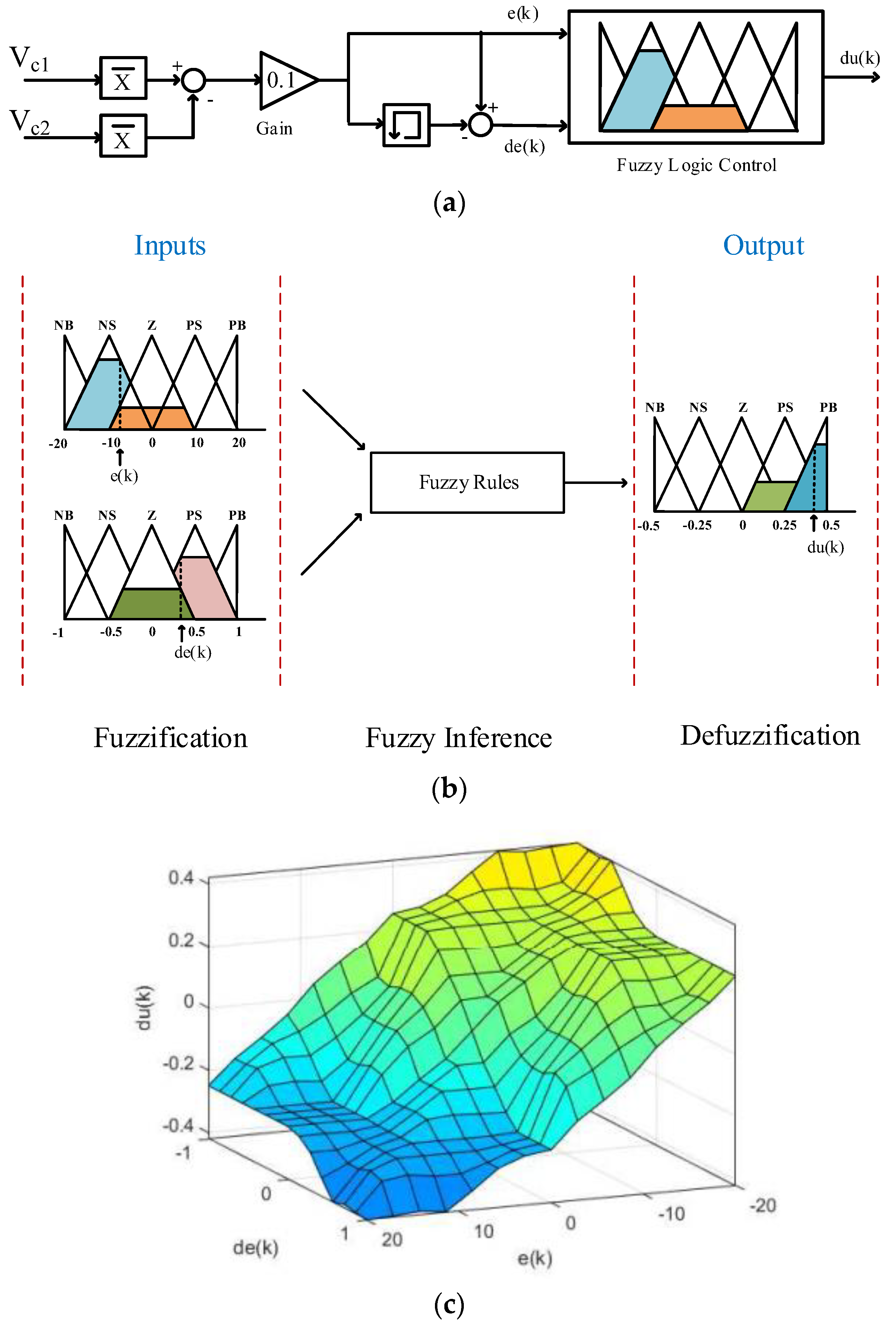
To thoroughly investigate the fluctuations in the DC bus capacitors, comprehensive simulation and experimental studies were conducted. The simulation analyses were performed using MATLAB/Simulink 2021a, while a laboratory-scale prototype test setup was developed to validate the findings experimentally.

3.1. Simulation Results

Comprehensive investigations were meticulously conducted to evaluate the various operating conditions of the three-phase grid-connected hybrid ANPC inverter system. The detailed parameters and specifications of this sophisticated system are thoroughly documented in Table 3, while the extensive scenarios examined throughout this research investigation are systematically presented in 
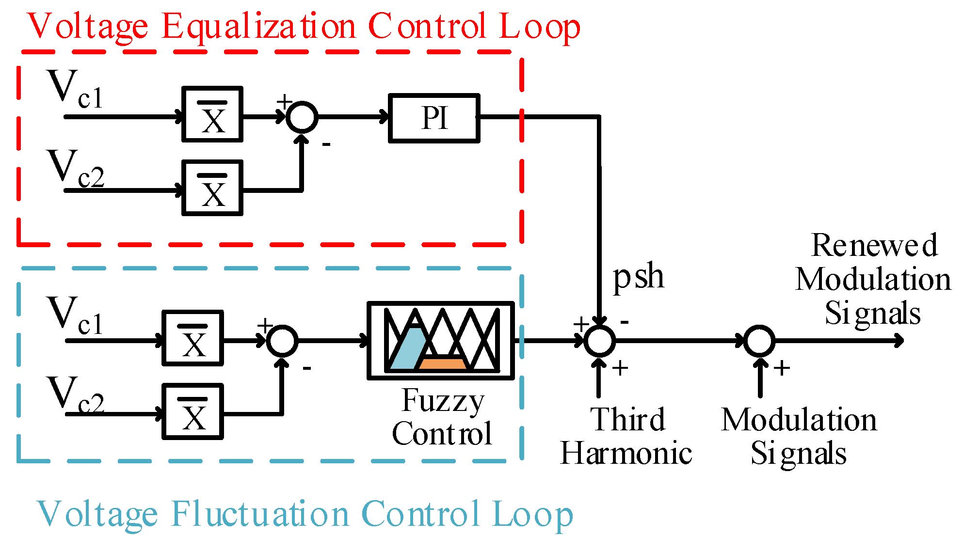
Table 4. To analyze the control of the 150 Hz fluctuation in the dc-link capacitor voltage, three different simulation studies were conducted. In the first scenario, no control was applied to this fluctuation. In the second scenario, an open-loop controller was designed using the THIPWM method. In the third scenario, the FLC was activated at a specific time interval in the simulation environment, and the system’s response both at the moment of the controller’s engagement and in subsequent instances was observed. For this comprehensive analysis, the system’s performance characteristics have been methodically evaluated through four distinct operational scenarios. During the initial phase of testing, specifically in the first scenarios (designated as Scenario-1), the SPWM technique was implemented as the primary modulation strategy, with the voltage fluctuation controller deliberately maintained in an inactive state. These conditions revealed notable voltage differentials between the initial capacitor voltages V c 1 and V c 2 , with measurements documented at 450 V–650 V, demonstrating significant variations in voltage distribution.
Progressing to Scenario-2 and Scenario-3, the research methodology incorporated a transition to the THIPWM technique, accompanied by the implementation of an open-loop control system architecture. Following these systematic modifications to the control strategy, the initial capacitor voltages V c 1   and V c 2 were carefully calibrated and maintained at a consistent level of 550 V.
The final phase of simulation, embodied in Scenario-4, introduced an enhanced control mechanism through the integration of a sophisticated fuzzy logic controller. This advanced configuration was subjected to an extended testing duration of 0.08 s to ensure comprehensive performance evaluation under sustained operational conditions. Throughout all scenarios, the PI controller remained consistently implemented within the voltage balancing loop, while the voltage fluctuation loop exhibited varying degrees of control sophistication across different scenarios—ranging from uncontrolled operation to open-loop configuration and ultimately culminating in the implementation of fuzzy logic control strategies.
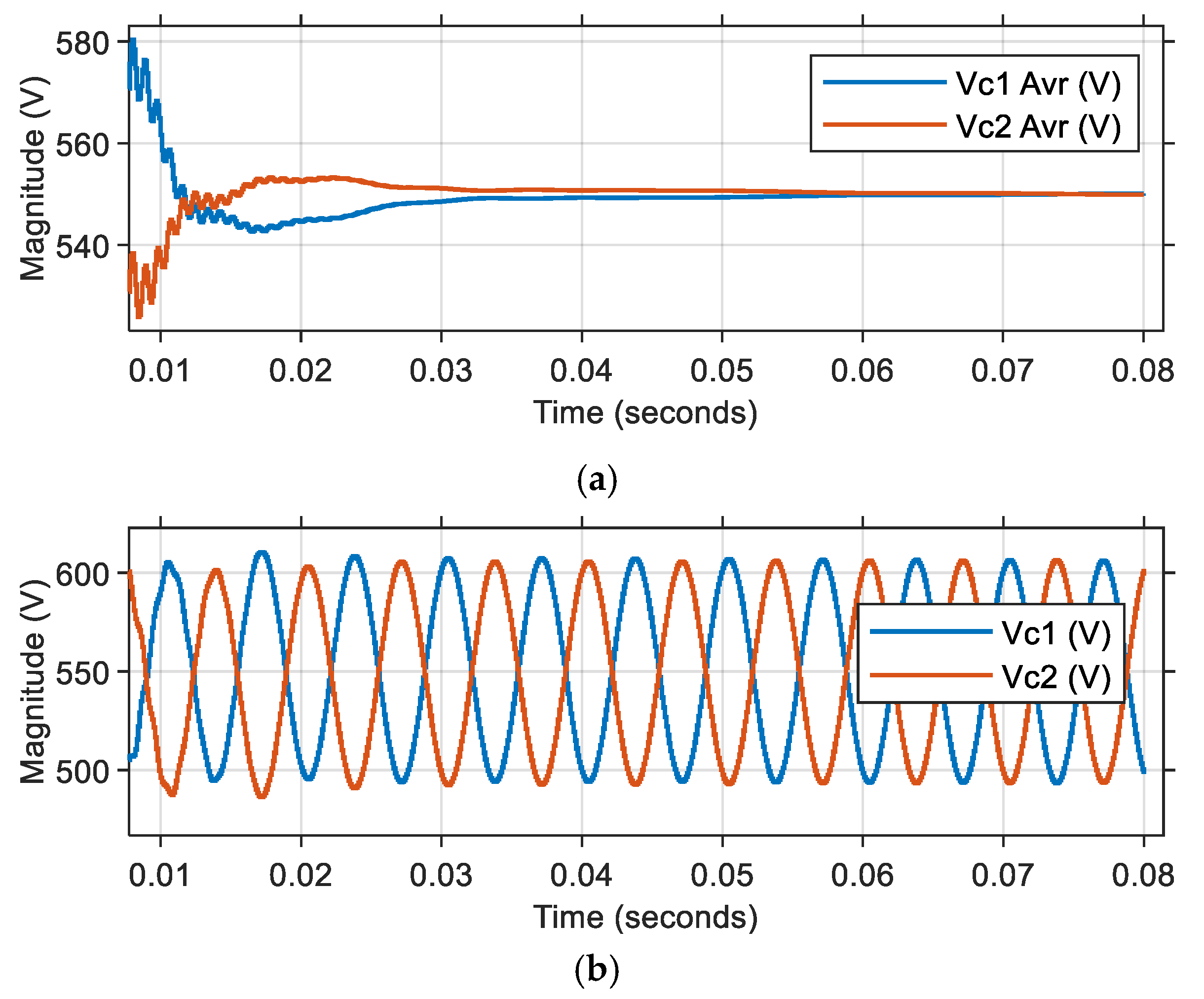
In Scenario-1, a comprehensive test was conducted within the specified time frame of 0 to 0.08 s to evaluate system performance under more challenging conditions. The initial capacitor voltage difference was deliberately increased to create a more demanding test environment. The initial voltage conditions were carefully configured, with V c 1 set to 450 V and V c 2 established at 650 V, creating a substantial initial voltage differential. The detailed simulation results and corresponding analysis for this scenario are thoroughly documented and presented in Figure 6.
In analyzing the results of Scenario-1, the careful examination of 
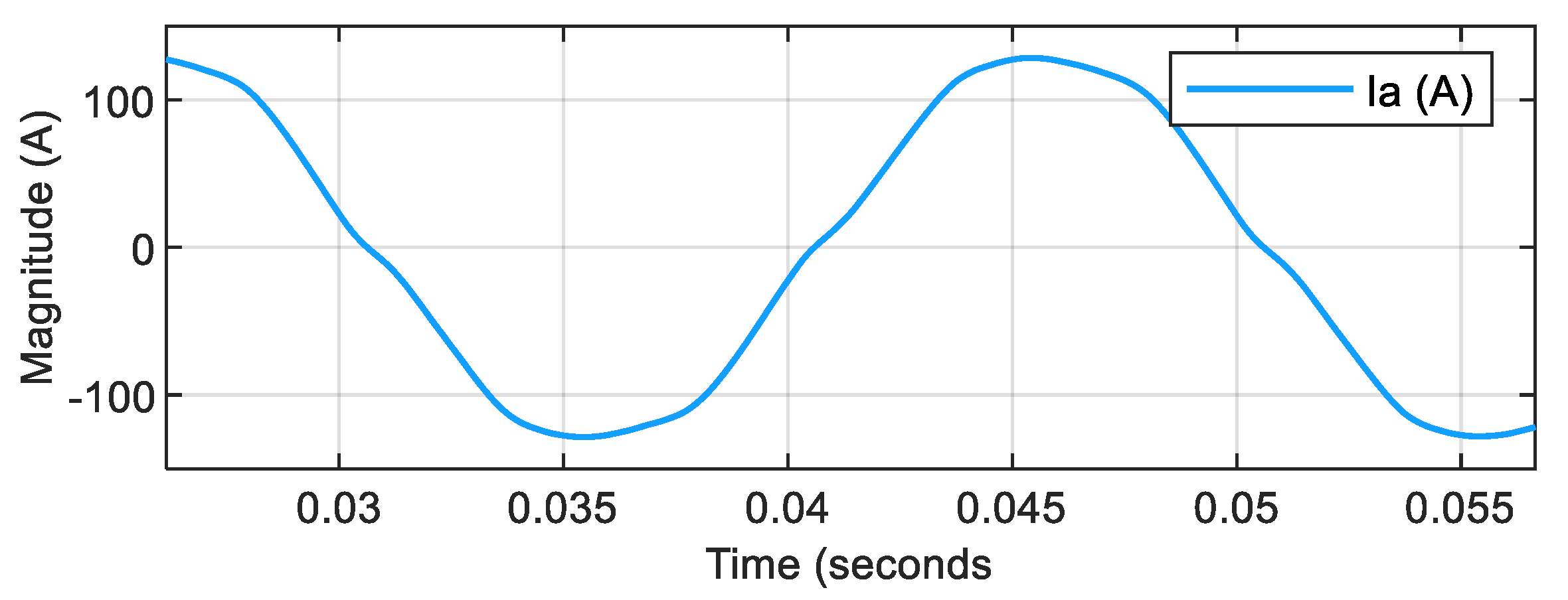
Figure 6 revealed that the process of equalizing the capacitor voltage values required a notably longer duration. Through precise measurements, the voltage settling time was determined to be 0.075 s, after which the steady-state average capacitor voltages stabilized at a measured value of 550 V. The further analysis of the voltage characteristics showed that the peak-to-peak voltage fluctuation maintained a consistent value of 120 V, while operating at a characteristic fluctuation frequency of 150 Hz. The current waveform of phase A injected into the grid is illustrated in 
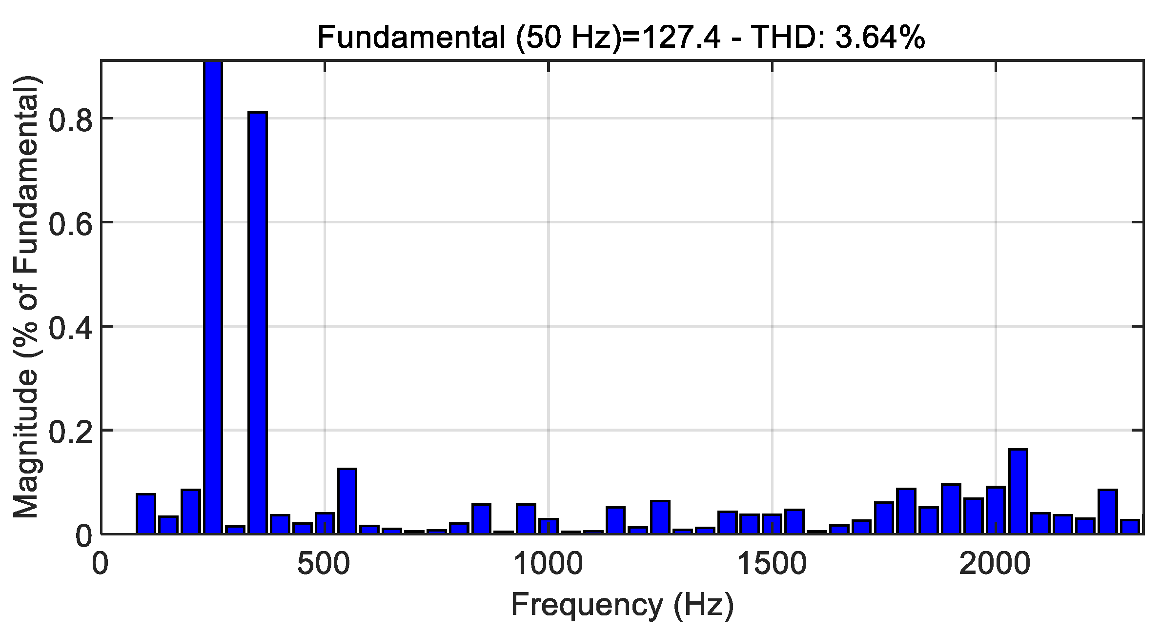
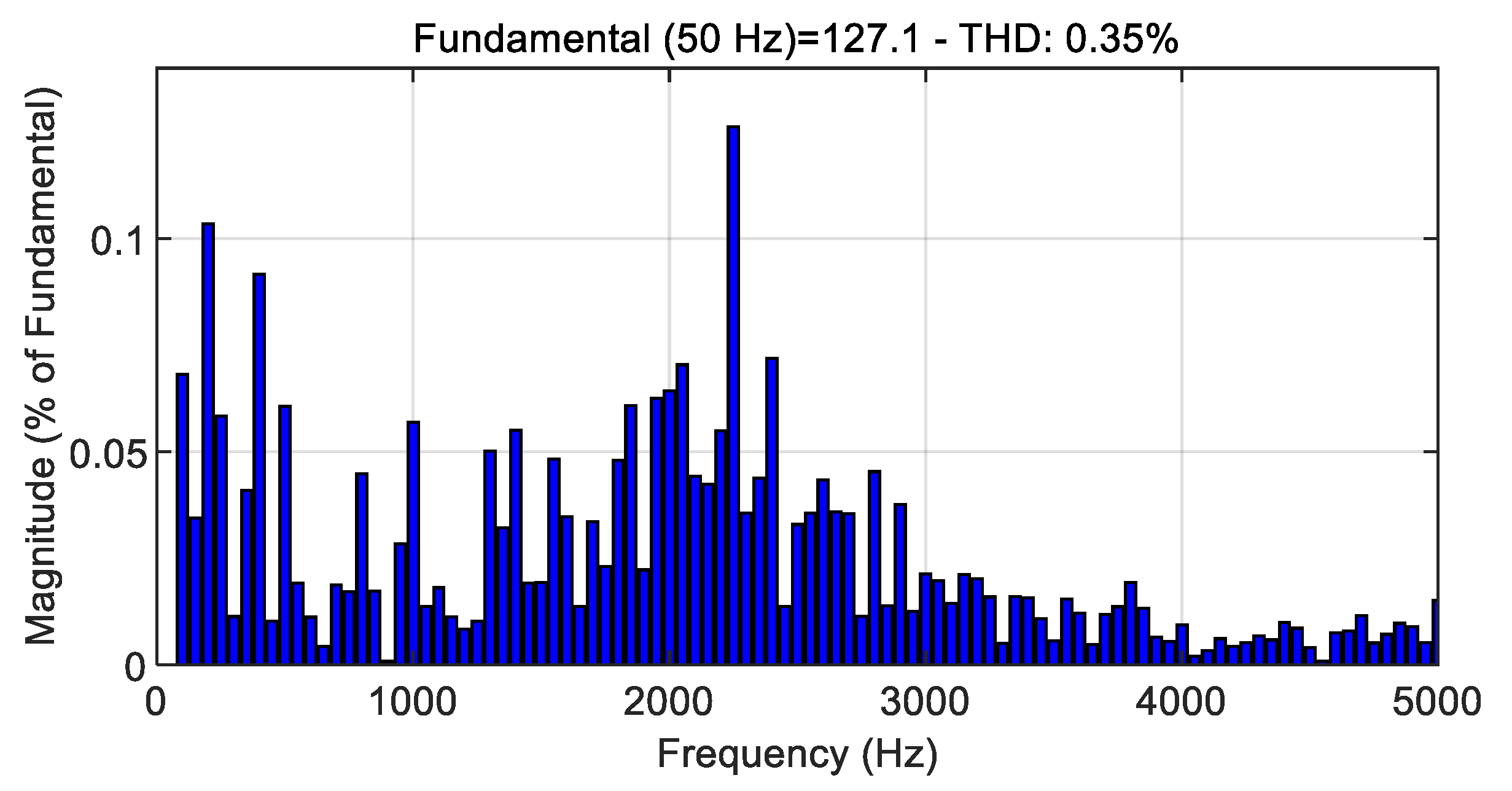
Figure 7. A comprehensive analysis of the power quality metrics was conducted, focusing on the THD distribution of the phase current in this sophisticated three-phase grid-connected hybrid ANPC inverter system. The detailed THD analysis, including the zoomed-in THD visualization, is comprehensively presented in Figure 8. Through careful measurement and analysis, the THD value of the phase current was precisely determined to be 3.64%, indicating excellent power quality characteristics.
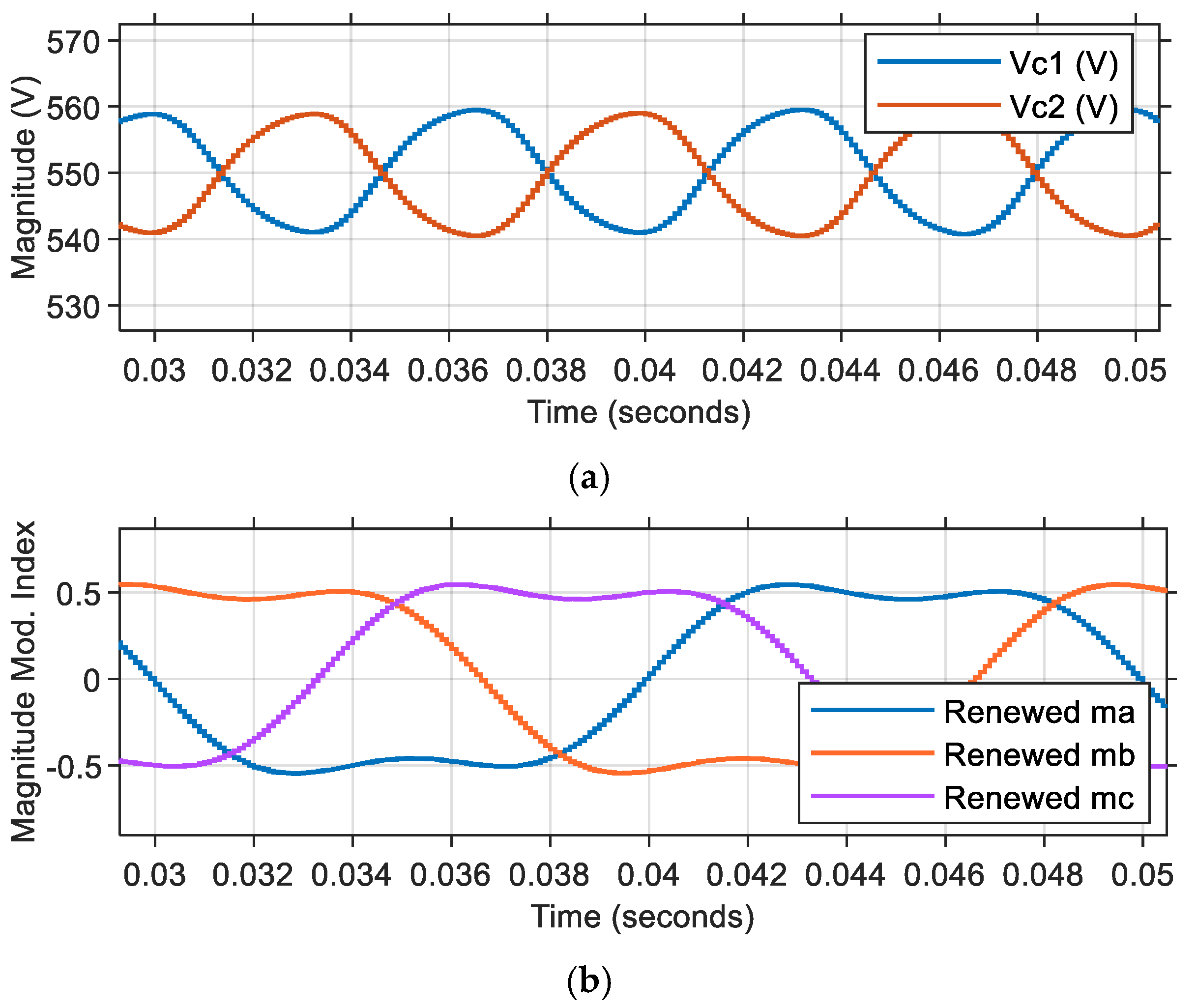
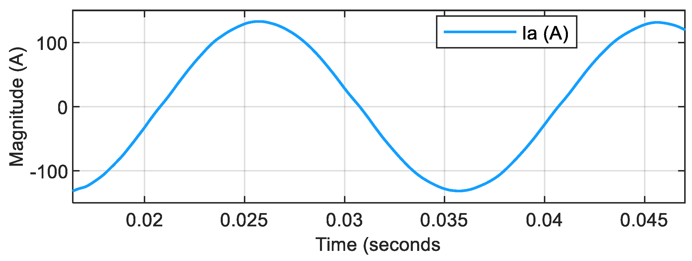
In Scenario-2, a comprehensive test was conducted within a carefully controlled time interval spanning from 0 to 0.05 s. For this particular scenario, the system configuration utilized a PI controller specifically implemented as the voltage equalizing loop controller, while the voltage fluctuation loop controller was deliberately maintained in open-loop configuration. The third-harmonic injection pulse-width modulation (THIPW) technique was selected as the preferred modulation method for this setup, and both capacitors in the system (designated as V c 1 and V c 2 ) were initialized with identical voltage values of 550 V. The detailed simulation results obtained from this system configuration are thoroughly documented and presented in Figure 9, Figure 10 and 
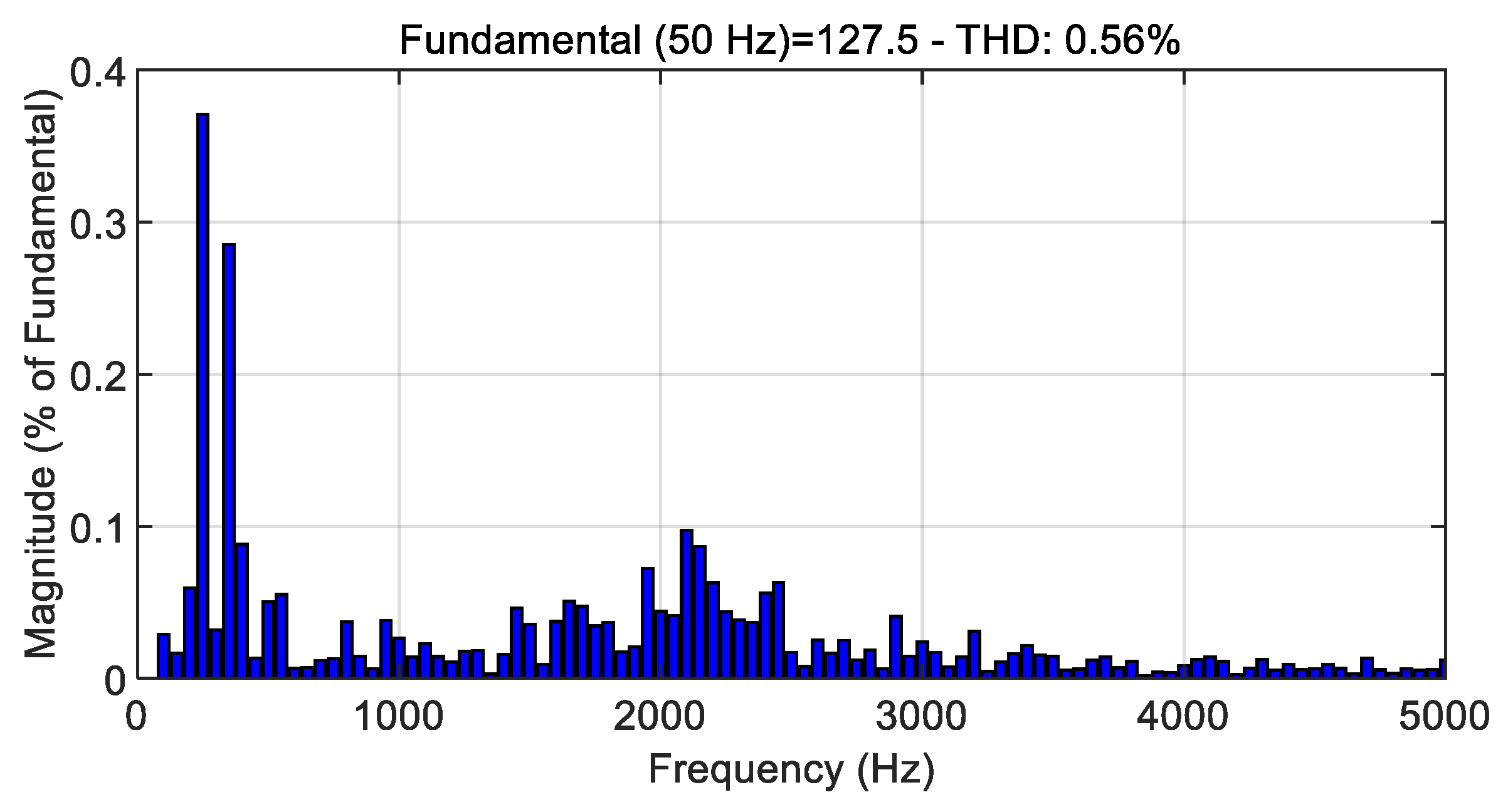
Figure 11. During the execution of Scenario-2, several significant performance metrics were carefully monitored and analyzed. The capacitor voltage demonstrated a settling time of precisely 0.045 s, after which the steady-state average capacitor voltage consistently maintained its initial value of 550 V throughout the test duration. A further analysis revealed that the voltage fluctuation characteristics exhibited a peak-to-peak magnitude of 18 V, occurring at a consistent frequency of 150 Hz. The comprehensive analysis of the system’s power quality metrics, particularly focusing on the THD distribution of the phase current in this hybrid ANPC inverter system, is extensively documented in Figure 11. The measurements indicate an exceptionally low THD value for the phase current, specifically calculated to be 0.56%, demonstrating the high quality of the power output.
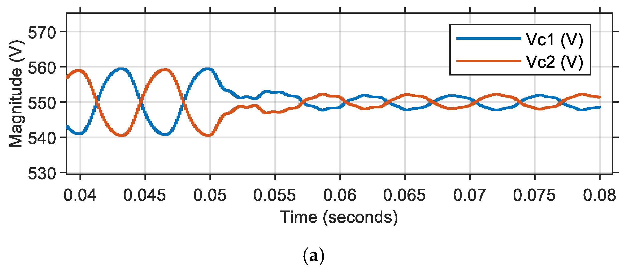
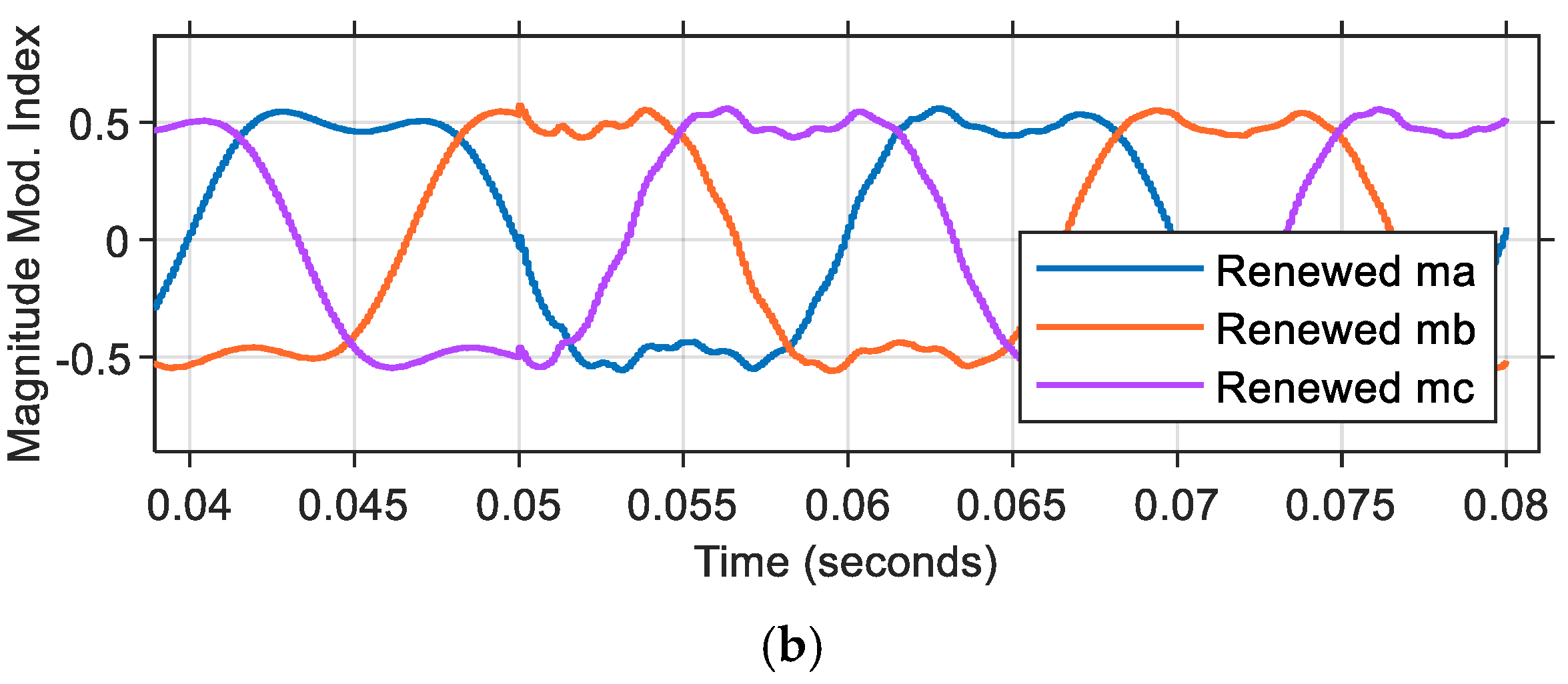
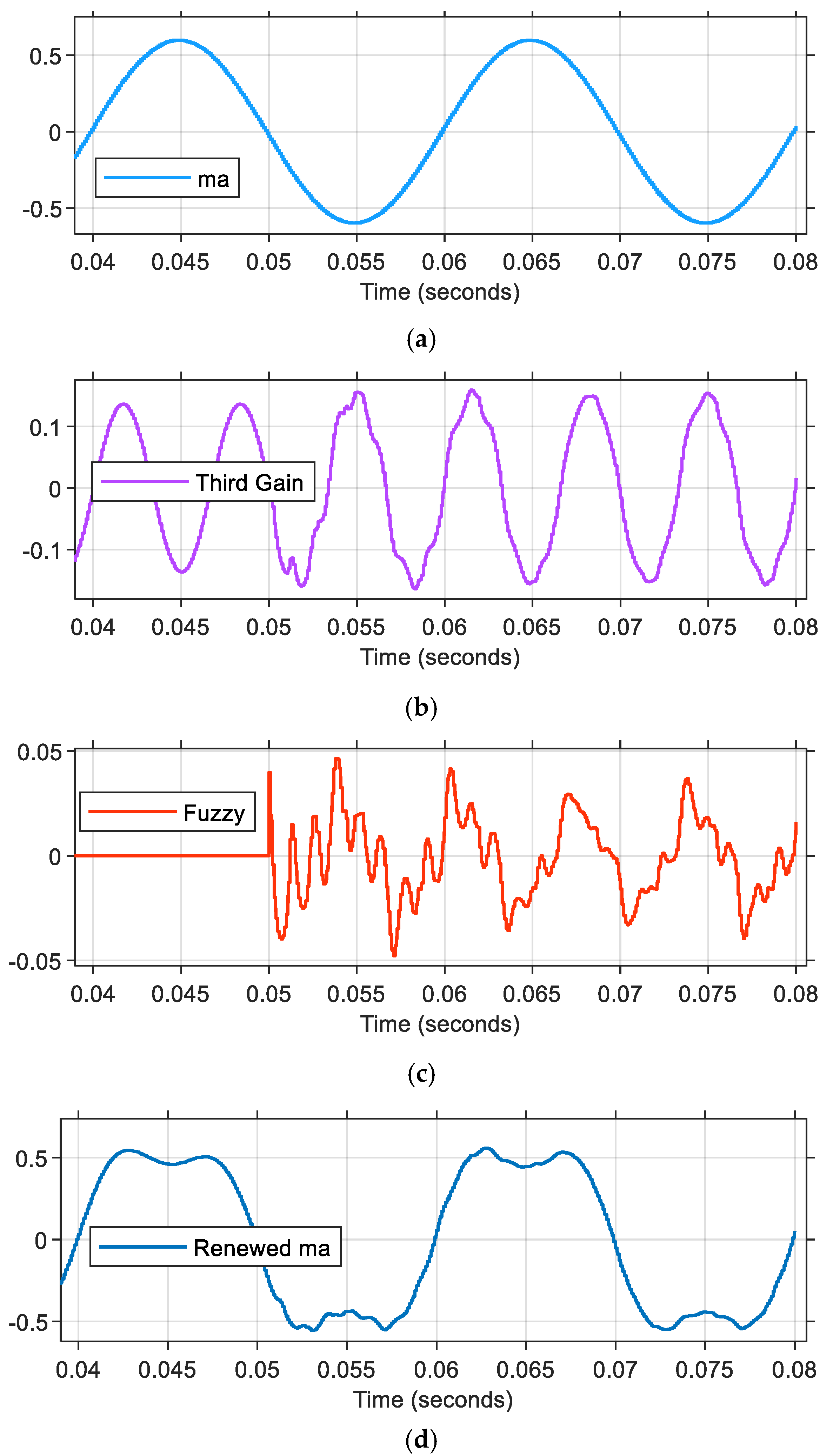
In Scenario-3, a comprehensive test was conducted within a precisely defined time interval spanning from 0 to 0.08 s. The simulation was strategically divided into two distinct phases of operation. During the initial phase, which encompassed the time interval from t = 0 to 0.05 s, the voltage fluctuation loop controller was configured to operate in open-loop mode. This was followed by a transition to the second phase, occurring in the interval from t = 0.05 to 0.08 s, during which a sophisticated fuzzy logic controller was implemented for managing voltage fluctuation control. Throughout the entire testing period, several key parameters were maintained to be constant to ensure simulation consistency. Specifically, the voltage equalization loop controller settings, the employed modulation technique, and the initial voltage values assigned to both capacitors (designated as V c 1 and V c 2 ) were kept identical to those utilized in Scenario-3. The comprehensive simulation results obtained from this simulation configuration were thoroughly documented and are presented in detail through Figure 12, Figure 13 and Figure 14. Some numerical results obtained from the conducted studies are presented in Table 5.

3.2. Experimental Results

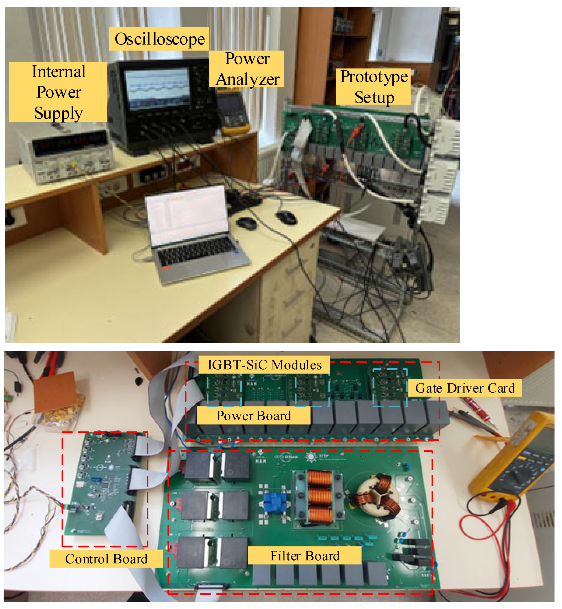
To validate the proposed advanced control technique, a laboratory prototype with a rated power of 62.5 kW was developed, mirroring the simulation setup. The parameters used for both simulation and experimental studies are presented in Table 3. Experimental conditions were replicated in the simulation environment as closely as possible; however, due to the grid-connected nature of the experimental tests, an exact real-time grid model could not be implemented in simulations. As a result, low-order voltage harmonics present in the actual grid led to slight discrepancies in THD measurements between the simulation and experimental results. Nevertheless, DC-link voltage ripple characteristics exhibited strong agreement between the two approaches.
The laboratory prototype used in the experimental study is illustrated in Figure 15, comprising the following
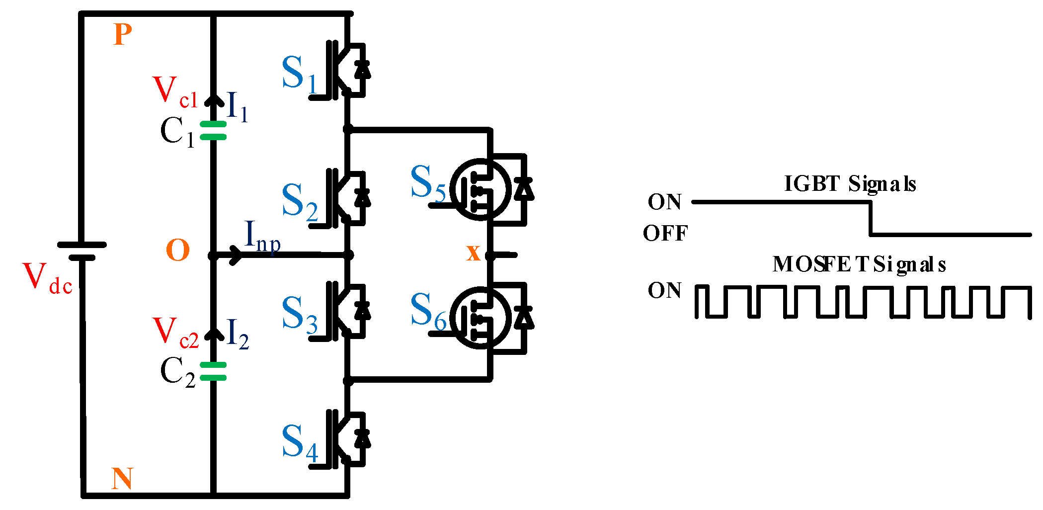
  • Power board: Features three “Vincotech B0-SP12NAA008ME01-LR88F78T” hybrid ANPC modules for the proposed topology, DC bus voltage measurement, and phase current routing.
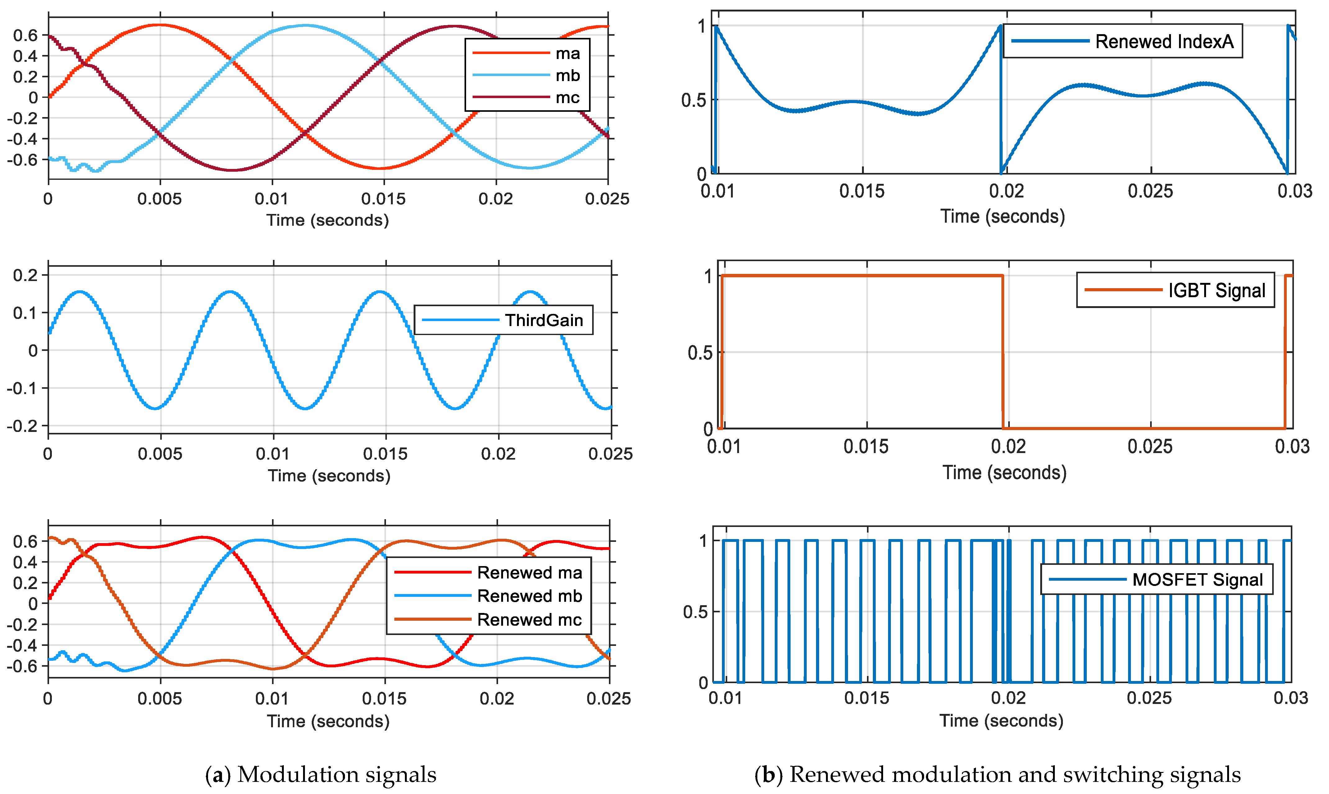
  • Control board: Hosts an STM32H723 550 MHz microcontroller for PWM signal generation, closed-loop control, cooling fan management, and analog measurements. Two DAC outputs enable real-time algorithm monitoring via an oscilloscope. The modulation index signals visible in the screen captures are acquired from the digital signal processor’s (DSP) digital-to-analog converter (DAC) output. These reference signals, which inherently vary between +1 and −1 in their normalized form, have been strategically scaled to a 0–3 V range through a linear transformation process. This scaling ensures optimal signal representation, with the zero-crossing point (x-axis) precisely aligned at the 1.5 V level, corresponding to the midpoint of the output range.
  • Driver board: Amplifies gate signals to drive the ANPC module’s IGBTs and SiC MOSFETs.
  • Filter board: Attenuates high-frequency switching noise and provides overcurrent protection.
  • A Fluke power analyzer is used to measure the THD of the phase current.
Three distinct experimental scenarios were designed and implemented to validate the theoretical framework. These scenarios are systematically presented in Table 6.
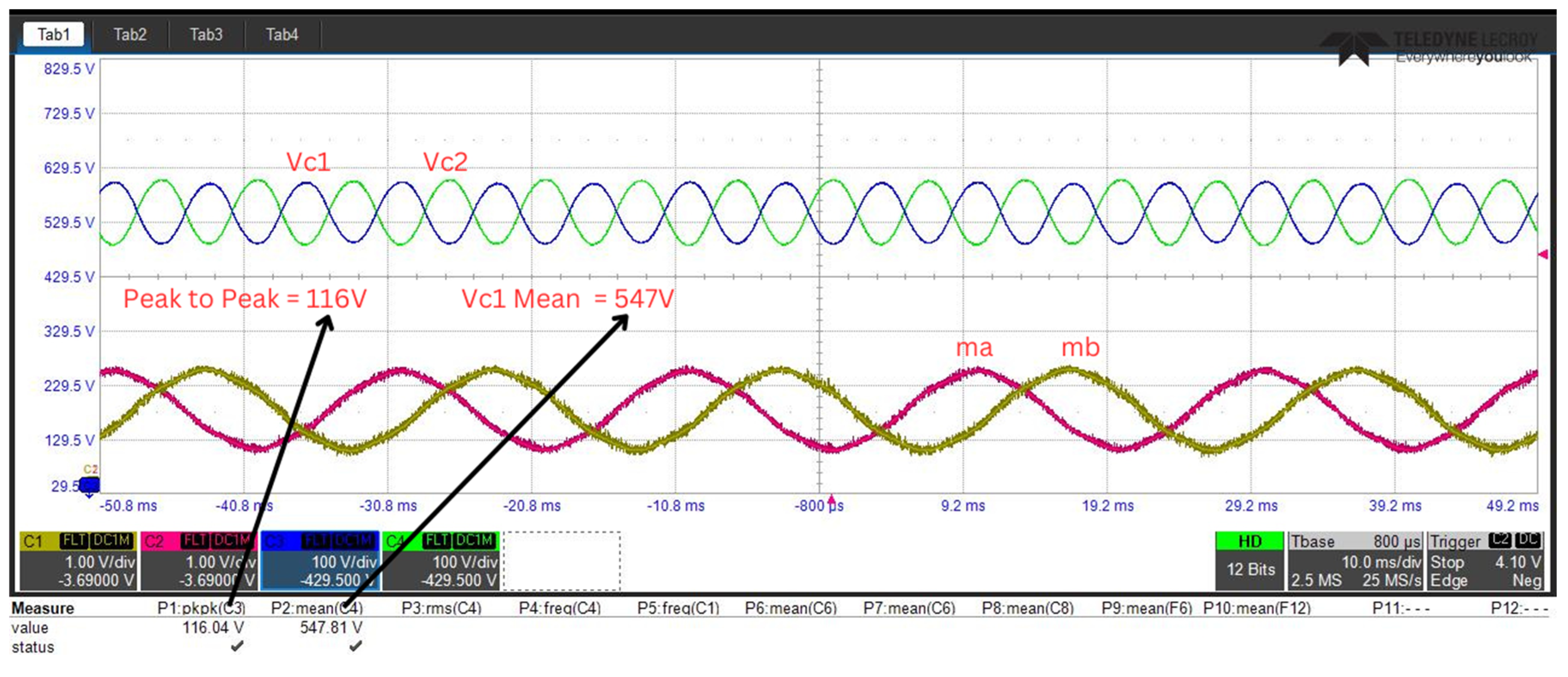
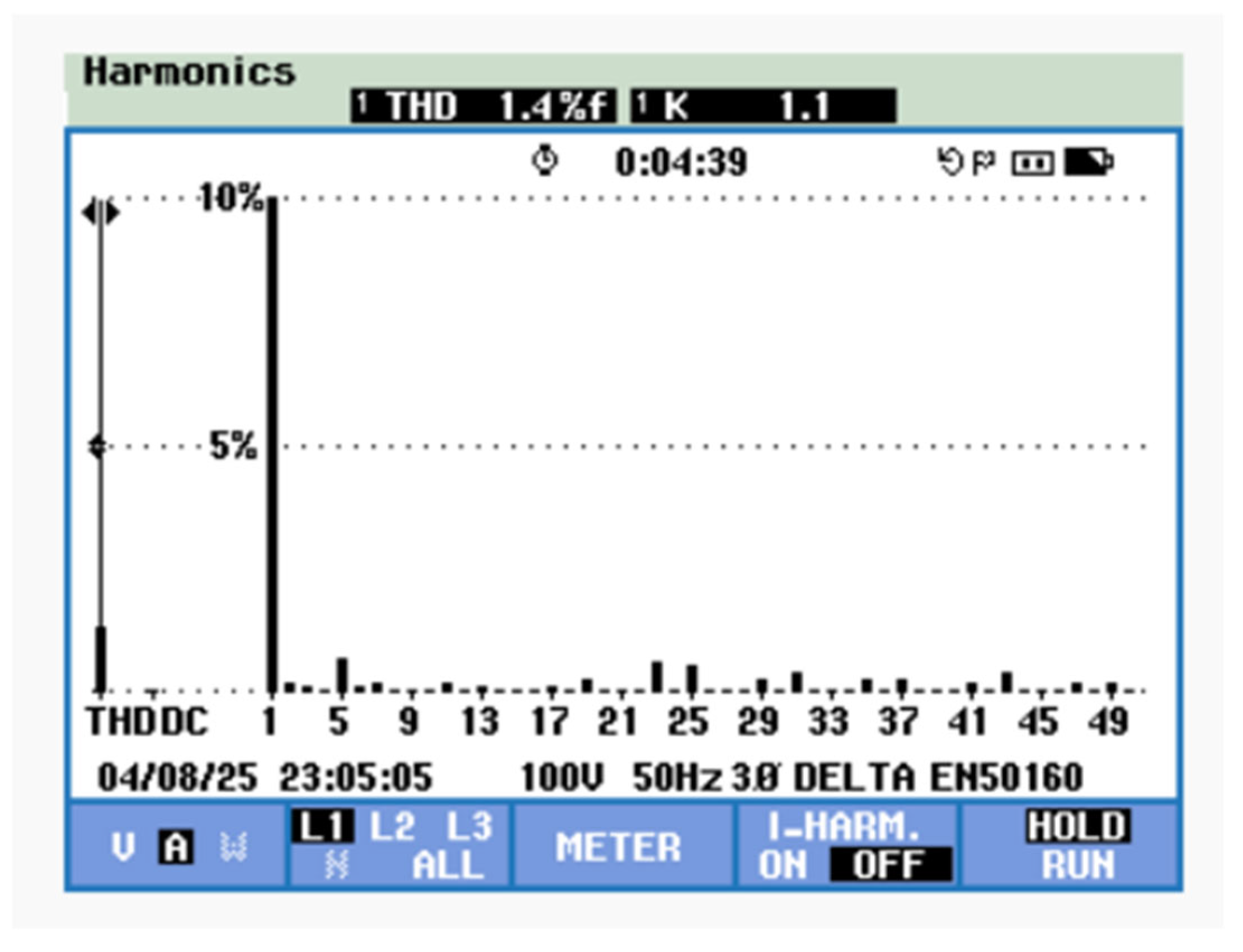
To analyze the control of the 150 Hz fluctuation in the dc-link capacitor voltage, three different experimental studies were conducted. In the first scenario, no control was applied for this oscillation. In the second scenario, an open-loop controller was designed using the THIPWM method. Finally, in the third scenario, a closed-loop FLC was designed. Under the first experimental configuration (Scenario 1), the voltage equalization control loop was maintained in an active operational state, while the voltage fluctuation suppression loop was deliberately deactivated for the duration of the testing period. The voltage balancing mechanism was governed exclusively by a PI control architecture to ensure precise voltage regulation across the capacitive elements.
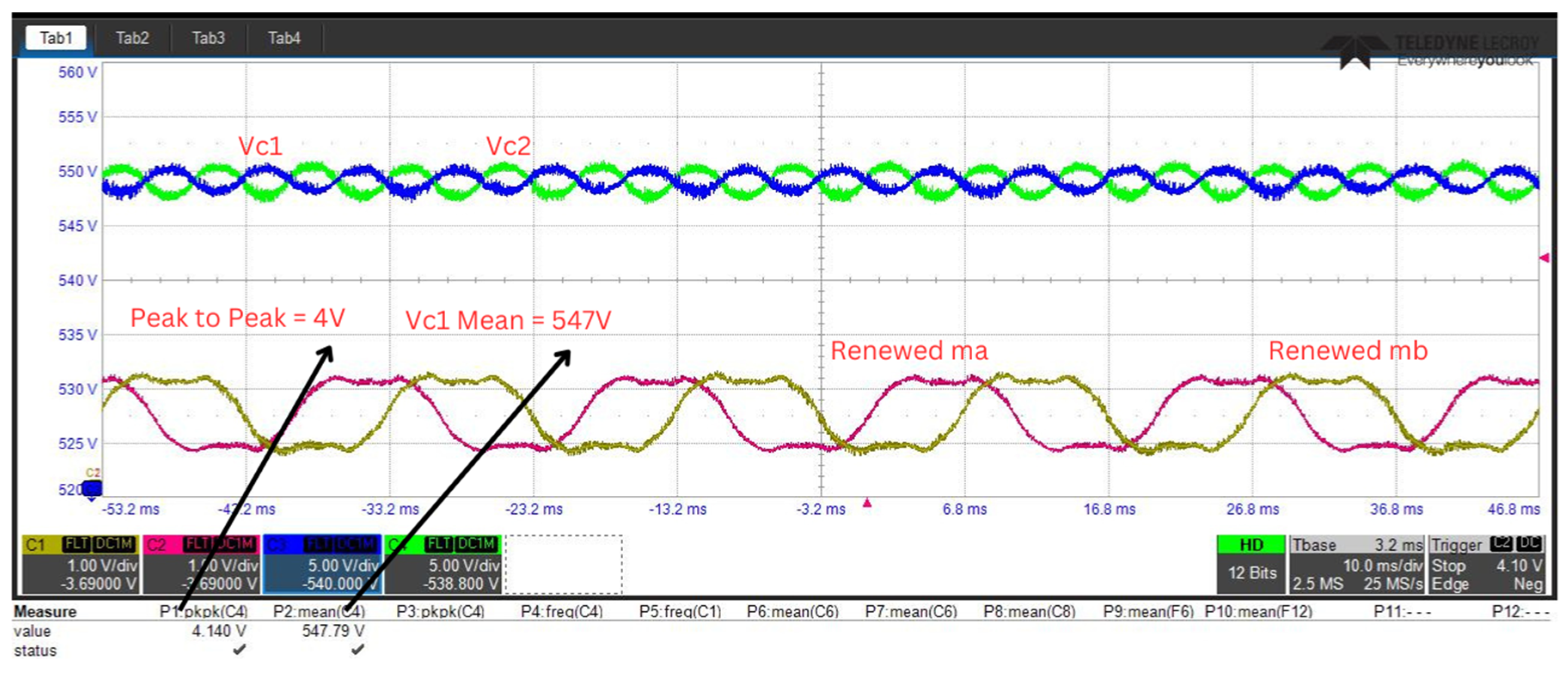
For this particular system configuration, SPWM was employed as the modulation strategy due to its well-documented advantages in harmonic suppression and implementation stability. The initial potential difference across the capacitive elements, denoted as ( V c 1 and V c 2 ), was carefully calibrated to an identical value of 547 V to establish uniform initial conditions.
The empirical results derived from this experimental configuration, which demonstrate the dynamic behavior and performance characteristics of the system under investigation, are comprehensively illustrated in Figure 16, Figure 17 and Figure 18. These graphical representations provide critical insights into the system’s operational efficacy under the specified control paradigm.
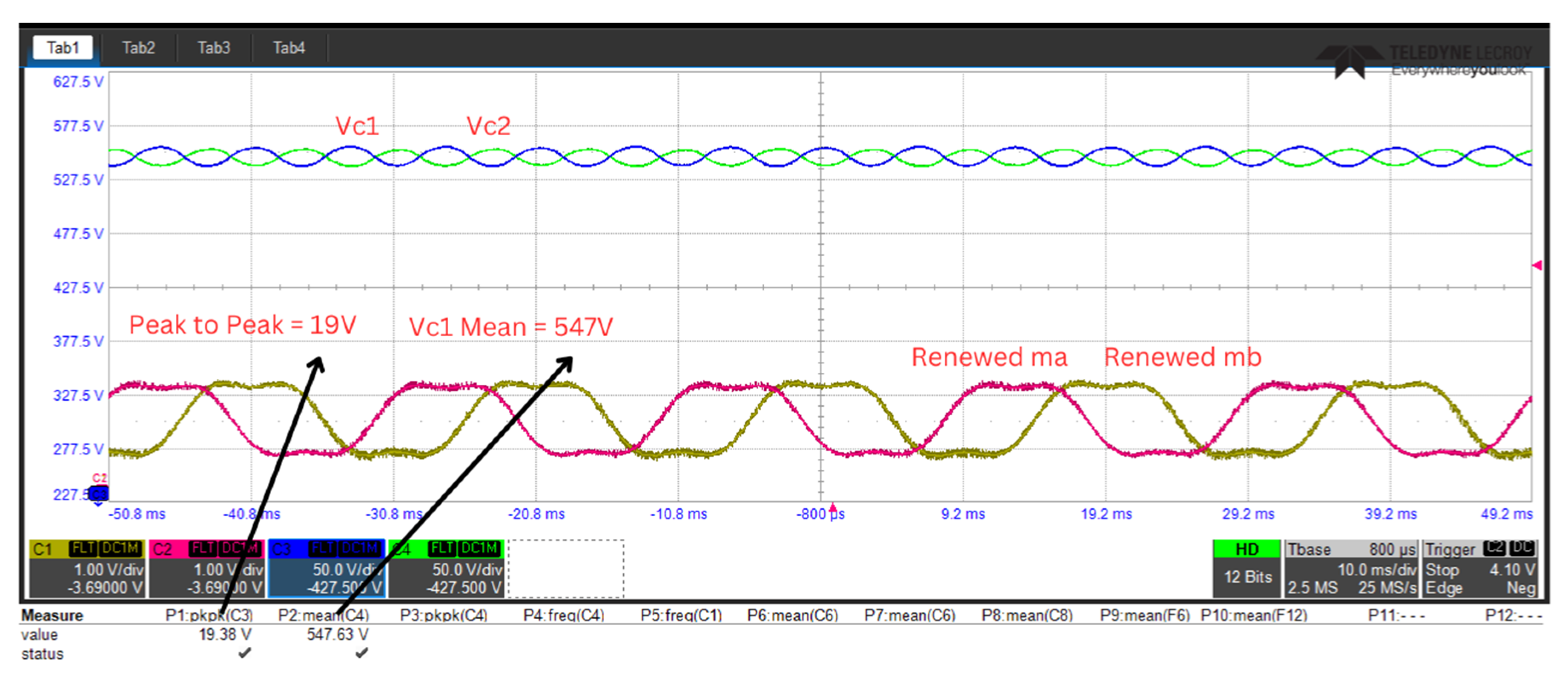
The second experimental scenario (Scenario-2) was precisely defined. In this configuration, the voltage equalization control loop was regulated by a PI control architecture, while the voltage fluctuation control loop system was intentionally maintained in an open-loop operational mode to isolate its effects. For the power conversion stage, the THIPWM technique was implemented as the modulation strategy, selected for its demonstrated efficacy in harmonic reduction and voltage utilization optimization. The initial charge distribution across both DC-link capacitors ( V c 1 and V c 2 ) was carefully balanced at 547 V to establish consistent initial operating conditions.
The experimental outcomes of this configuration, which reveal critical insights into the system’s dynamic response characteristics under these specific control parameters, are presented with analytical rigor in Figure 19 and Figure 20. These graphical representations comprehensively illustrate the temporal evolution of the key electrical parameters throughout the investigation period.
The third experimental scenario (Scenario 3) incorporated a hybrid control architecture to evaluate comparative performance metrics. The voltage equalization loop continued to employ a PI control scheme, while the voltage fluctuation mitigation system was upgraded to utilize an FLC in conjunction with THIPWM. This advanced configuration was designed to investigate potential synergistic effects between intelligent control algorithms and optimized modulation techniques.
Consistent with previous experimental protocols, the initial potential difference across both capacitive elements ( V c 1 and V c 2 ) was precisely initialized at 547 V to maintain methodological continuity. The comprehensive experimental results, which demonstrate the enhanced performance characteristics achieved through this sophisticated control strategy, are systematically presented in Figure 21, Figure 22 and Figure 23 These visual representations provide compelling evidence of the system’s improved stability and dynamic response when employing the proposed control paradigm.
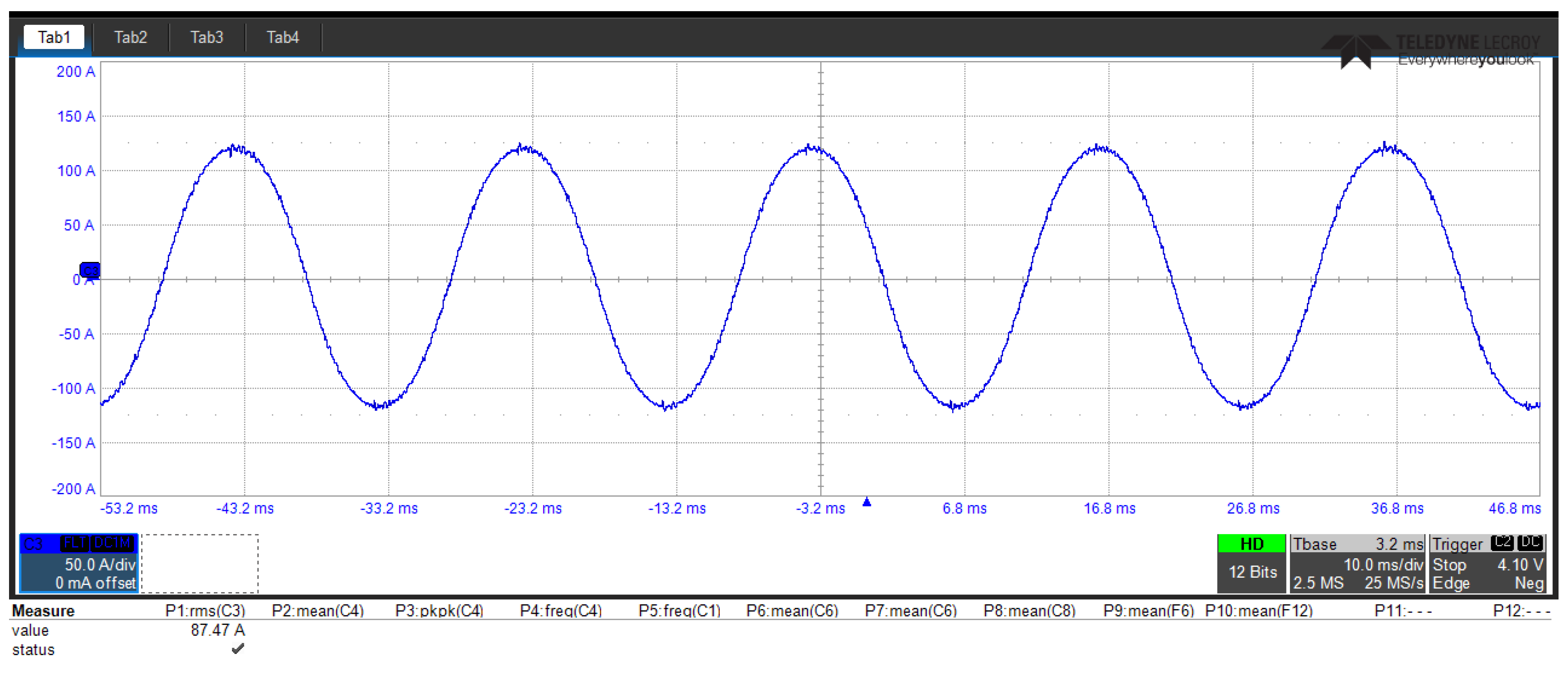
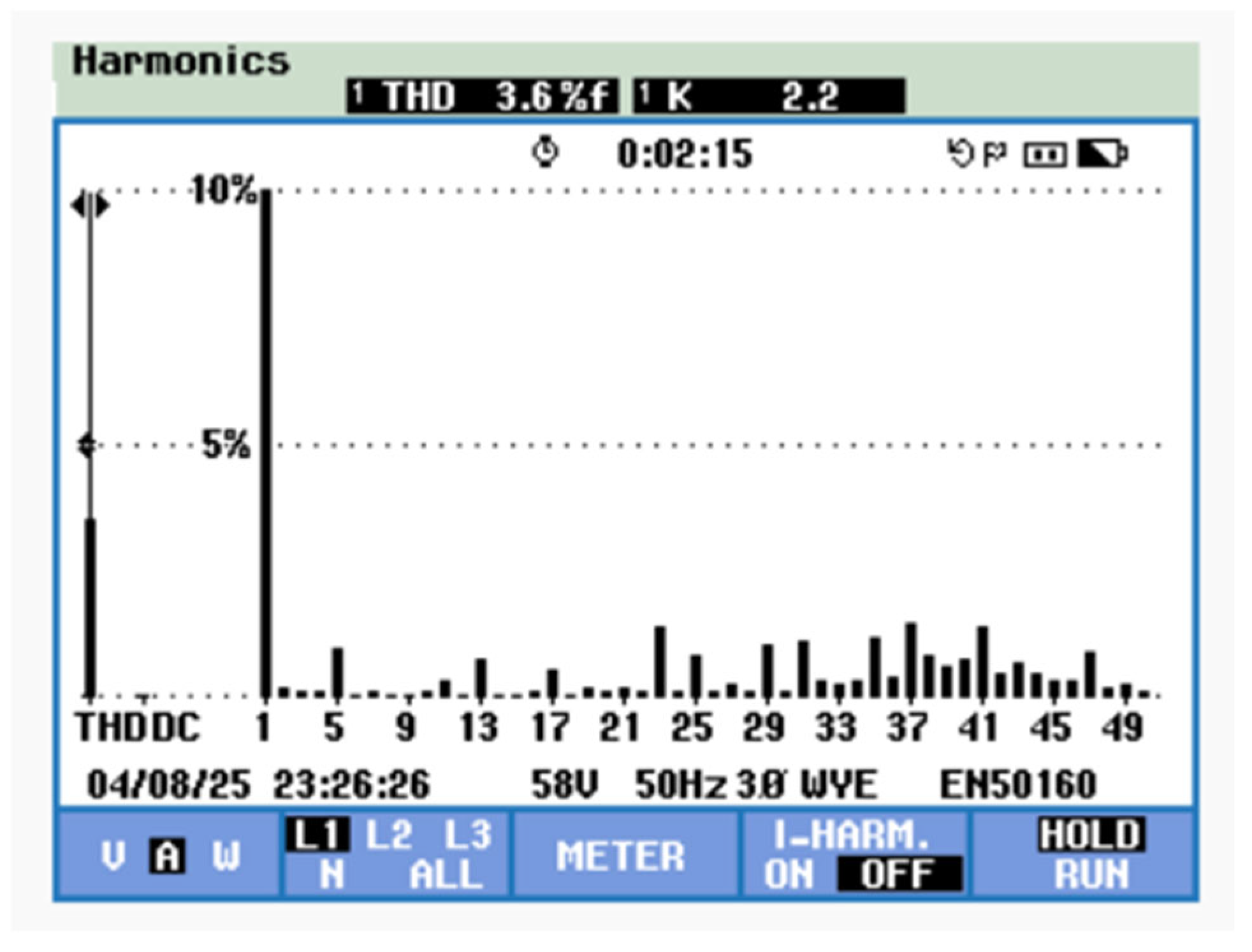
A rigorous examination of the Scenario-1 experimental results revealed several critical performance characteristics of the hybrid ANPC inverter system. The detailed analysis of the voltage waveform characteristics demonstrated that the peak-to-peak voltage fluctuation exhibited remarkable stability, maintaining a consistent amplitude of 116 V throughout operation. This fluctuation occurred at a well-defined characteristic frequency of 150 Hz, reflecting the system’s inherent dynamic behavior under the specified control configuration.
The investigation extended to a thorough evaluation of power quality metrics, with a particular emphasis on THD characteristics in this advanced three-phase grid-connected configuration. As systematically presented in Figure 18, the spectral analysis of phase current distortion reveals excellent harmonic performance characteristics. Precision measurements conducted under controlled laboratory conditions yielded a phase current THD of precisely 3.6%, a value that confirms exceptional power quality compliance with international standards for grid-connected power electronic systems.
Complementing these findings, Figure 17 presents an oscilloscope capture of the actual phase current waveform during system operation. This visual representation provides crucial empirical evidence of the current waveform, serving to validate the quantitative THD measurements through direct observation.
The combined analytical results from both quantitative THD assessment and qualitative waveform examination collectively demonstrate that the implemented control strategy successfully achieves power quality while maintaining stable voltage characteristics under the specified operating conditions. These findings establish a strong foundation for comparative performance evaluation with the subsequent experimental scenarios.
The second experimental scenario (Scenario-2) was systematically executed to evaluate the system’s performance under modified control conditions. In this configuration, the voltage equalization mechanism was regulated by a PI control architecture, while the voltage fluctuation control loop system was intentionally maintained in an open-loop configuration to isolate its effects on system dynamics.
The power conversion stage employed THIPWM as the modulation strategy, selected for its superior harmonic suppression capabilities in three-phase systems. Conditions were carefully established with both DC-link capacitors ( V c 1 and V c 2 ) precisely balanced at 547 V. During steady-state operation, the capacitor voltages demonstrated exceptional stability, maintaining an average value of 547 V with minimal deviation.
The detailed analysis of voltage characteristics revealed a well-regulated peak-to-peak voltage fluctuation amplitude of 19 V, oscillating at a characteristic frequency of 150 Hz. This represents a significant reduction in the voltage ripple compared to previous configurations, highlighting the effectiveness of the implemented control strategy.
Comprehensive power quality assessment, as illustrated in Figure 20, demonstrates outstanding current harmonic performance. The spectral analysis of the phase current yielded a remarkably low THD of just 1.4%, establishing new benchmarks for power quality in grid-connected hybrid ANPC inverter systems. This exceptional performance represents an approximately 61% improvement in THD compared to the Scenario-1 results.
The experimental outcomes, systematically presented in Figure 19 and Figure 20, provide compelling evidence of the system’s enhanced performance characteristics. Figure 19 presents detailed oscillography measurements of the key operational parameters, while Figure 20 offers a comprehensive spectral analysis of the current waveforms. Together, these results validate the superior harmonic suppression capabilities achieved by THIPWM in this configuration.
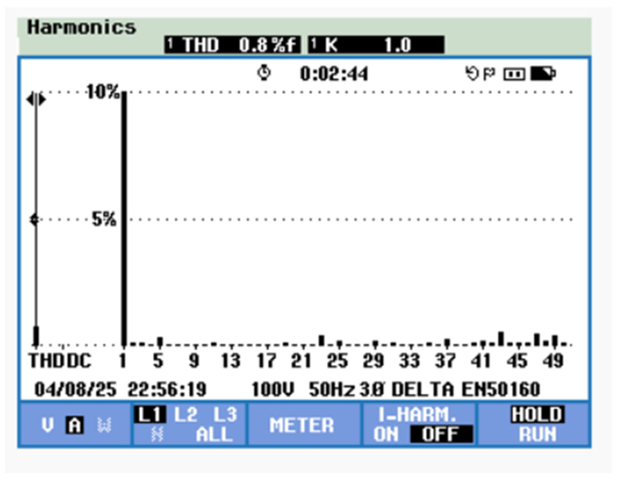
The final experimental scenario (Scenario-3) was conducted to assess the system’s performance under an advanced control architecture. This configuration employed a PI controller for the voltage equalization loop while implementing a fuzzy logic controller for voltage fluctuation suppression, combined with THIPWM. The mean capacitor voltages ( V c 1 and V c 2 ) were carefully balanced at 547 V to maintain consistent experimental conditions.
System performance metrics demonstrated exceptional results in this configuration. The steady-state average capacitor voltages remained precisely at 547 V, showing perfect voltage balancing capability. Voltage fluctuation analysis revealed a remarkably low peak-to-peak variation of just 4 V at the characteristic 150 Hz frequency, representing a significant improvement over the previous scenario. This minimal fluctuation amplitude underscores the effectiveness of the FLC and THIPWM approach in suppressing voltage fluctuations.
The comprehensive experimental results, presented in Figure 21, Figure 22 and Figure 23, provide a complete characterization of the system’s behavior under this optimal control configuration. 
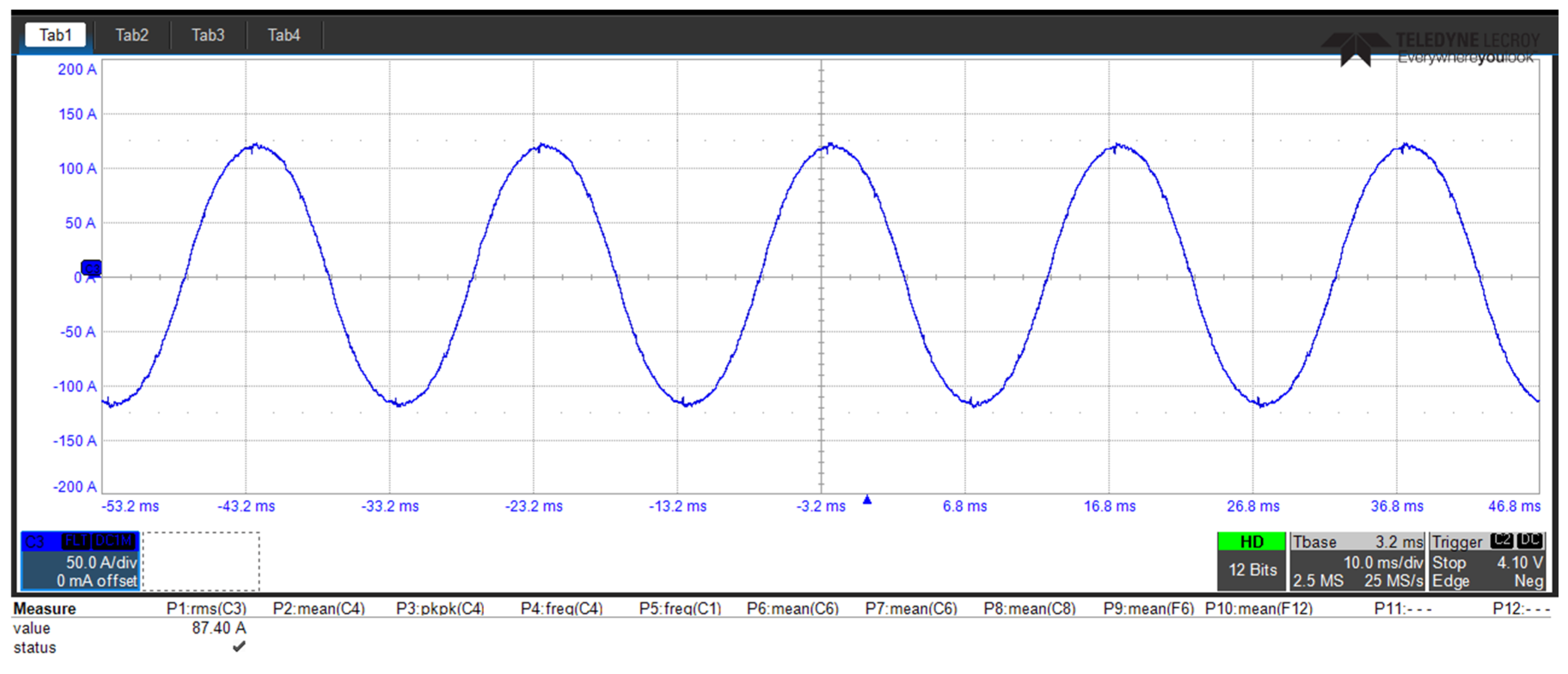
Figure 22 displays the system’s dynamic response and voltage regulation performance, while Figure 22 presents the exceptionally clean sinusoidal waveform of the phase current, demonstrating the system’s ability to produce low-harmonic output with negligible distortion. Figure 23 complements this with a detailed spectral analysis of the output current waveform, quantitatively confirming the outstanding 0.80% THD performance. Together, these results validate the advanced control architecture as an optimal solution for achieving both excellent voltage stability and superior power quality in three-phase grid-connected ANPC inverter systems. The progressive improvement observed across all three scenarios clearly demonstrates the effectiveness of the implemented control strategies, with Scenario-3 establishing new performance benchmarks for such power electronic systems. The waveform purity visible in Figure 22, combined with the spectral evidence in Figure 23, provides irrefutable proof of the system’s ability to meet the most stringent power quality requirements while maintaining robust voltage regulation. Some numerical results obtained from the conducted studies are presented in Table 7.

4. Conclusions

A comprehensive comparative analysis of this study with similar research initiatives from the literature was conducted, specifically examining three crucial parameters: THD, DC bus capacitor specifications, and voltage fluctuation characteristics. The experimental results are systematically presented and thoroughly documented in Table 8, which compares the findings of the proposed method with those of five distinct research studies. This current investigation particularly distinguishes itself through its innovative approach to DC bus capacitor optimization and exceptional performance in current harmonic distortion reduction. The strategic decrease in the quantity of implemented DC bus capacitors resulted in a substantial reduction in the overall system costs, making this solution particularly attractive from an economic perspective.
Both experimental and simulation studies were carried out to evaluate DC-link ripple and THD performance, with consistent results observed in DC-link voltage fluctuations. However, due to non-ideal grid conditions (including grid voltage harmonics) in the experimental tests, the current THD was slightly higher compared to the simulation results. In the operational analysis of the system, measurements indicate that the DC bus capacitors supply the inverter with approximately 59 amperes RMS. Based on conventional design principles and the mathematical framework established in Equation (12) derived from the detailed system analysis, the theoretical calculations suggested that a capacitor with a substantial capacity of 7.8 mF would be necessary to effectively manage and compensate for a voltage fluctuation of 4 volts. However, through the implementation of an advanced and meticulously engineered controller structure developed specifically for this study, equivalent operational performance was remarkably achieved using a significantly smaller 0.3 mF capacitor. This breakthrough represents an extraordinary enhancement in capacitor size optimization, achieving an approximately 26-fold reduction in capacity requirements. The successful implementation of these considerably lower-capacity capacitors led to a dramatic decrease in overall system costs. Moreover, the proposed control strategy reduced the peak-to-peak DC-link voltage ripple from 116 V to just 4 V, and the total harmonic distortion (THD) of the phase current was lowered from 3.6% to 0.8%.
The successful minimization of voltage fluctuation has yielded multiple significant benefits throughout the system. Primarily, it has substantially extended the operational lifespan of the capacitors while simultaneously achieving remarkable improvements in current harmonic distortion characteristics within the system. Additionally, the effective control of voltage fluctuation throughout the system has resulted in notably reduced voltage variations across power electronic switching components. This enhancement ensures that these critical switching elements consistently operate within their designated safe operating parameters and maintains robust protection against potentially hazardous voltage conditions. The solution method developed and successfully implemented in this study was primarily demonstrated and validated for ANPC-based inverter systems. However, it also offers a universal design approach that can be readily applied to three-level neutral-point-clamped inverter systems based on similar principles.
The integration of newly incorporated components into the system inherently introduces the phenomenon of common-mode current generation. In centralized inverter systems, each inverter is typically connected to a dedicated medium-voltage (MV) transformer. On the inverter side, these transformers are designed with an ungrounded (floating) configuration. To mitigate the effects of common-mode voltages, a grounded conductive layer, such as an aluminum foil or other suitable conductive material, is placed between the primary and secondary windings of the transformer. This situation is more complex for solar string inverter applications, compared to centralized inverter systems. This is primarily because the transformer’s inverter-side windings are often grounded. As a result, common-mode currents can flow from the transformer’s grounded input, pass through the leakage capacitances of the PV modules, and return to the inverter. This circulating current must be carefully managed to comply with international standards. To suppress these common-mode currents, it is necessary to implement dedicated common-mode filters. The cost of these filters is relatively low compared to DC-link capacitors. Also, the addition of a THIPWM signal introduces additional circulating currents, particularly at 150 Hz, in the AC cables. This leads to an increase in power losses due to the skin effect, when compared to conventional PWM schemes. The common-mode current discussed is depicted in Figure 24.

Author Contributions

Conceptualization, all authors; methodology, all authors; software, all authors; validation, all authors; formal analysis, all authors; investigation, all authors; resources, all authors; data curation, all authors; writing—original draft preparation, all authors; writing—review and editing, all authors; visualization, all authors; supervision, all authors. All authors have read and agreed to the published version of the manuscript.

Funding

This study has been supported by 20AG002 of 1004—Center of Excellence Support Program organized by Scientific and Technological Research Council of Türkiye (TUBITAK).

Data Availability Statement

The original contributions presented in the study are included in the article, further inquiries can be directed to the corresponding authors.

Conflicts of Interest

The authors declare no conflicts of interest.

Nomenclature

SymbolDescriptionUnit
VdcDC-Link VoltageVolt
VgPhase-to-Phase Voltage of AC Grid Volt
Vc1Upper Capacitor VoltageVolt
Vc2Lower Capacitor VoltageVolt
IaA Phase Line CurrentAmpere
RiInverter-Side Internal Resistance of InductorOhm
LiInverter-Side InductorHenry
RgGrid-Side Internal Resistance of InductorOhm
LgGrid-Side InductorHenry
RTThe Sum of Resistance Ri and Rg Ohm
LTThe Sum of inductance Li and Lg Henry
RfESR of CapacitorOhm
CfCapacitor of LCL filter Farad
PLLPhase Locked Loop
mModulation Index
mttRenewed Index Modulation Signals
m0 and m3Fundamental and Third Modulation Signal, respectively
Va, Vb, and VcPhase-to-Neutral Voltage for Each PhaseVolt
Ed, and Eqdq Transformation Corresponding to Each Phase-Neutral VoltageVolt
Id and Iqdq Transformation Corresponding to Phase Current Ampere

References

  1. Kim, G.; Lee, H.; Shon, J. Enhanced Harmonic Reduction and Voltage Utilization Ratio Improvement in ANPC Inverters Using an Advanced Hybrid SVPWM Technique. Energies 2025, 18, 1868. [Google Scholar] [CrossRef]
  2. Ben Mahmoud, Z.; Khedher, A. A Comprehensive Review on Space Vector Based-PWM Techniques for Common Mode Voltage Mitigation in Photovoltaic Multi-Level Inverters. Energies 2024, 17, 916. [Google Scholar] [CrossRef]
  3. Cavli, N.; Ozkop, E. Performance Analysis of Modulation Strategies in Single-Phase HBNPC Inverter Across Variable Operating Conditions. IEEE Access 2024, 12, 65997–66013. [Google Scholar] [CrossRef]
  4. Radomsky, L.; Keilmann, R.; Ferch, D.; Mallwitz, R. Challenges and Opportunities in Power Elec. Design for All- and Hybrid-Electric Aircraft: A Qualitative Review and Outlook. CEAS Aeronaut. J. 2024, 15, 751–764. [Google Scholar] [CrossRef]
  5. Yurievich, V.B.; Hien, N.T. Stochastic Pulse-Width Modulation and Modification of Direct Torque Control Based on a Three-Level Neutral-Point Clamped Inverter. Energies 2024, 17, 6017. [Google Scholar] [CrossRef]
  6. Wang, H.; Ha, L.; Lin, J.; Wang, S.; Xie, S.; Chen, X.; Su, M. A Mathematical Structural Modulation Method for Neutral-Point Potential Balancing of Three-Level Neutral-Point-Clamped Converters. IEEE J. Emerg. Sel. Top. Power Electron. 2024, 12, 1573–1582. [Google Scholar] [CrossRef]
  7. Le, H.-P.N.; Pham, K.D.; Nguyen, N. Analyses, Modeling, and SVPWM Control of a Three-Level T-NPC Inverter to Reduce Common-Mode Voltage Under Open-Circuit Fault in a Neutral-Point Switch. IEEE Access 2024, 12, 104708–104727. [Google Scholar] [CrossRef]
  8. Ogan, S.E.; Bostanci, E. Capacitor Sizing of Three-level Neutral Point Clamped Voltage Source Inverter for Electric Vehicles: Effects of Modulation and Motor Characteristics. IET Power Electron. 2024, 17, 1051–1066. [Google Scholar] [CrossRef]
  9. Roy, P.; Kurre, M.; Charan Nannam, H.; Banerjee, A. Reliability Evaluation of Carrier-based Pulse Width Modulated Three-level F-type Neutral Point Clamped Inverter with Power Loss Analysis. Int. J. Circuit Theory Appl. 2024, 52, 162–187. [Google Scholar] [CrossRef]
  10. Alepuz, S.; Busquets-Monge, S.; Nicolás-Apruzzese, J.; Filbà-Martínez, À.; Bordonau, J.; Yuan, X.; Kouro, S. A Survey on Capacitor Voltage Control in Neutral-Point-Clamped Multilevel Converters. Electronics 2022, 11, 527. [Google Scholar] [CrossRef]
  11. Wu, M.; Wang, K.; Pou, J.; Yang, K.; Zheng, Z.; Li, Y. Topology and Control of Seven-Level Tree-Type Active Neutral-Point-Clamped Converters. IEEE Trans. Ind. Electron. 2025, 72, 3257–3268. [Google Scholar] [CrossRef]
  12. Dong, Z.; Wang, C.; Li, Z. Four-Degree-of-Freedom Hybrid Control Strategy for the Neutral-Point Voltage of Three-Level NPC Multiphase Inverter. IEEE Trans. Power Electron. 2024, 39, 6745–6757. [Google Scholar] [CrossRef]
  13. Hasan, N.S.; Rosmin, N.; Osman, D.A.A.; Musta’amal@Jamal, A.H. Reviews on Multilevel Converter and Modulation Techniques. Renew. Sustain. Energy Rev. 2017, 80, 163–174. [Google Scholar] [CrossRef]
  14. Guo, F.; Ma, Z.; Diao, F.; Zhao, Y.; Wheeler, P. Hybrid Virtual Coordinate-Driven CBPWM Strategy of Three-Level T-Type NPC Converters for Electric Aircraft Propulsion Applications. IEEE Trans. Ind. Electron. 2024, 71, 2309–2319. [Google Scholar] [CrossRef]
  15. Halabi, L.M.; Hakami, S.S.; Lee, K.-B. Integrated Voltage Vector–Based SVPWM for Reliability and Performance Enhancement of Five-Level HANPC Inverters. IEEE Trans. Ind. Electron. 2024, 71, 1093–1103. [Google Scholar] [CrossRef]
  16. Bahrami, A.; Narimani, M. A Sinusoidal Pulsewidth Modulation (SPWM) Technique for Capacitor Voltage Balancing of a Nested T-Type Four-Level Inverter. IEEE Trans. Power Electron. 2019, 34, 1008–1012. [Google Scholar] [CrossRef]
  17. Srivastava, S.; Chaudhari, M.A. Comparison of SVPWM and SPWM Schemes for NPC Multilevel Inverter. In Proceedings of the 2020 IEEE International Students’ Conference on Electrical, Electronics and Computer Science (SCEECS), Bhopal, India, 22–23 February 2020; pp. 1–6. [Google Scholar]
  18. Subsingha, W. A Comparative Study of Sinusoidal PWM and Third Harmonic Injected PWM Reference Signal on Five Level Diode Clamp Inverter. Energy Procedia 2016, 89, 137–148. [Google Scholar] [CrossRef]
  19. Rabiul Islam, M.; Mahfuz-Ur-Rahman, A.M.; Muttaqi, K.M.; Sutanto, D. State-of-the-Art of the Medium-Voltage Power Converter Technologies for Grid Integration of Solar Photovoltaic Power Plants. IEEE Trans. Energy Convers. 2019, 34, 372–384. [Google Scholar] [CrossRef]
  20. Tcai, A.; Shin, H.-U.; Lee, K.-B. DC-Link Capacitor-Current Ripple Reduction in DPWM-Based Back-to-Back Converters. IEEE Trans. Ind. Electron. 2018, 65, 1897–1907. [Google Scholar] [CrossRef]
  21. Hossain, S.; Biswas, S.P.; Mondal, S.; Nath, J.; Islam, M.R.; Shah, R. Advanced Voltage Balancing Discontinuous PWM Technique for Solar PV Fed Grid-Tied NPC Inverters. IEEE Trans. Appl. Supercond. 2024, 34, 5402805. [Google Scholar] [CrossRef]
  22. Zaragoza, J.; Pou, J.; Ceballos, S.; Robles, E.; Ibanez, P.; Villate, J.L. A Comprehensive Study of a Hybrid Modulation Technique for the Neutral-Point-Clamped Converter. IEEE Trans. Ind. Electron. 2009, 56, 294–304. [Google Scholar] [CrossRef]
  23. Busquets Monge, S.; Somavilla, S.; Bordonau, J.; Boroyevich, D. Capacitor Voltage Balance for the Neutral-Point-Clamped Converter Using the Virtual Space Vector Concept with Optimized Spectral Performance. IEEE Trans. Power Electron. 2007, 22, 1128–1135. [Google Scholar] [CrossRef]
  24. Basak, S.; Paul, S.; Dholakia, A.; Ghotgalkar, S.; Basu, K. A Carrier-Based Implementation of a Nearest Three Space-Vector PWM Strategy of Three-Level Inverter. In Proceedings of the 2022 IEEE International Conference on Power Electronics, Drives and Energy Systems (PEDES), Jaipur, India, 14 December 2022; pp. 1–7. [Google Scholar]
  25. Kumar, B.H.; Janardhan, K.; Kumar, R.S.; Rahul, J.R.; Singh, A.R.; Naidoo, R.; Bansal, R.C. An Enhanced Space Vector PWM Strategies for Three Phase Asymmetric Multilevel Inverter. Int. Trans. Electr. Energy Syst. 2023, 2023, 548828. [Google Scholar] [CrossRef]
  26. Ozciflikci, O.E.; Koc, M. Comparison of Interior Mounted Permanent Magnet Synchronous Motor Drives with Sinusoidal, Third Harmonic Injection, and Space Vector Pulse Width Modulation Strategies with Particular Attention to Current Distortions and Torque Ripples. Electrica 2023, 23, 151–159. [Google Scholar] [CrossRef]
  27. Du To, D.; Lee, D.-C. Hybrid PWM Technique and Capacitor Voltage Balancing Control for Four-Level Asymmetrical Flying Capacitor Inverter. IEEE Access 2025, 13, 31401–31410. [Google Scholar] [CrossRef]
  28. Jiao, Y.; Lee, F.C.; Lu, S. Space Vector Modulation for Three-Level NPC Converter with Neutral Point Voltage Balance and Switching Loss Reduction. IEEE Trans. Power Electron. 2014, 29, 5579–5591. [Google Scholar] [CrossRef]
  29. Yuan, Q.; Qian, J.; Li, A. A Simplified Common-Mode Voltage Suppression and Neutral-Point Potential Control for the NPC Three-Level Inverter. J. Electr. Eng. Technol. 2019, 14, 2389–2398. [Google Scholar] [CrossRef]
  30. An, S.-W.; Kim, S.-M.; Lee, K.-B. Capacitor Lifetime Extension in a Hybrid Active Neutral-Point-Clamped Inverter with Reduction of DC-Link Ripple Current and Common-Mode Voltage. IEEE Access 2021, 9, 40336–40348. [Google Scholar] [CrossRef]
  31. Hakami, S.S.; Halabi, L.M.; Lee, K.-B. Dual-Carrier-Based PWM Method for DC-Link Capacitor Lifetime Extension in Three-Level Hybrid ANPC Inverters. IEEE Trans. Ind. Electron. 2023, 70, 3303–3314. [Google Scholar] [CrossRef]
  32. Liu, P.; Duan, S.; Yao, C.; Chen, C. A Double Modulation Wave CBPWM Strategy Providing Neutral-Point Voltage Oscillation Elimination and CMV Reduction for Three-Level NPC Inverters. IEEE Trans. Ind. Electron. 2018, 65, 16–26. [Google Scholar] [CrossRef]
  33. Hossain, S.; Prokash Biswas, S.; Mondal, S.; Islam, M.R.; Fekih, A. A Capacitor Voltage Balancing Hybrid PWM Technique to Improve the Performance of T-Type NPC Inverters. IEEE Access 2024, 12, 87545–87559. [Google Scholar] [CrossRef]
  34. Liserre, M.; Dell’Aquila, A.; Blaabjerg, F. Stability Improvements of an LCL-Filter Based Three-Phase Active Rectifier. In Proceedings of the 2002 IEEE 33rd Annual IEEE Power Electronics Specialists Conference. Proceedings (Cat. No. 02CH37289), Cairns, Australia, 23–27 June 2002; pp. 1195–1201. [Google Scholar]
  35. Abdelmalik, Z.; Barkat, S.; Sangwongwanich, A. Neutral point voltage balancing control based on adjusting application times of redundant vectors for three-level NPC inverter. IEEE J. Emerg. Sel. Top. Power Electron. 2022, 10, 5604–5613. [Google Scholar] [CrossRef]
Figure 1. General block diagram of the inverter.
Energies 18 03143 g001
Figure 2. Modulation and switching signals.
Energies 18 03143 g002
Figure 3. Single-phase topology and switching strategy of a three-phase ANPC inverter.
Energies 18 03143 g003
Figure 4. Voltage equalization and fluctuation controller block diagram.
Energies 18 03143 g004
Figure 5. Fuzzy logic controller structure. (a) FLC detailed block diagram. (b) Detailed FLC parameters. (c) Output signals according to input signals.
Energies 18 03143 g005
Figure 6. V c 1 and V c 2 capacitor voltage waveforms (simulation results—Scenario-1): (a) average; (b) actual.
Energies 18 03143 g006
Figure 7. Phase-A line current (Ia) waveform (simulation results—Scenario-1).
Energies 18 03143 g007
Figure 8. Zoomed THD of single-phase current (ampere) (simulation results—Scenario-1).
Energies 18 03143 g008
Figure 9. Waveforms (simulation results—Scenario-2): (a) average capacitor voltages V c 1 and V c 2 ; (b) modulation signal.
Energies 18 03143 g009
Figure 10. Ia phase line current waveform (simulation results—Scenario-2).
Energies 18 03143 g010
Figure 11. THD of single-phase current (ampere) (simulation results—Scenario-2).
Energies 18 03143 g011
Figure 12. Waveforms (simulation results—Scenario-3): (a) average capacitor voltages V c 1 and V c 2 ; (b) modulation signal.
Energies 18 03143 g012aEnergies 18 03143 g012b
Figure 13. Voltage fluctuation control loop waveforms (simulation results—Scenario-3): (a) fundamental modulation signal, (b) third-harmonic gain, (c) fuzzy logic controller output signal du(k), and (d) renewed modulation signal.
Energies 18 03143 g013
Figure 14. THD of single-phase current (ampere) (simulation results—Scenario-3).
Energies 18 03143 g014
Figure 15. Picture of the laboratory test bench.
Energies 18 03143 g015
Figure 16. V c 1 and V c 2 are actual capacitor voltage waveforms (C3–C4)—ma and mb are the modulation indexes (C1–C2) (experimental results—Scenario-1).
Energies 18 03143 g016
Figure 17. Ia phase line current waveform (experimental results—Scenario-1).
Energies 18 03143 g017
Figure 18. THD of single-phase current (experimental results—Scenario-1).
Energies 18 03143 g018
Figure 19. V c 1 and V c 2 are the actual capacitor voltage waveforms (C3–C4)—ma and mb are the modulation indexes (C1–C2) (experimental results—Scenario-2).
Energies 18 03143 g019
Figure 20. THD of single-phase current (experimental results—Scenario-2).
Energies 18 03143 g020
Figure 21. V c 1 and V c 2 are the actual capacitor voltage waveforms (C3–C4)—ma and mb are the modulation indexes (C1–C2) (experimental results—Scenario-3).
Energies 18 03143 g021
Figure 22. Ia phase current waveform (experimental results—Scenario-3).
Energies 18 03143 g022
Figure 23. THD of single-phase current (experimental results—Scenario-3).
Energies 18 03143 g023
Figure 24. Common-mode current loop.
Energies 18 03143 g024
Table 1. Switch states.
State S 1 S 2 S 3 S 4 S 5 S 6 U x o
P101010 0.5   V d c
OU10100100
OU20110100
OU30010010
OU40110010
N010101 0.5   V d c
Table 2. Fuzzy rule base for output signals (du(k)).
e/deNBNSZPSPB
NBNBNBNSNSZ
NSNBNSNSZPS
ZNSNSZPSPS
PSNSZPSZNS
PBZPSPSPBPB
Table 3. System parameters for simulation and experimentation.
SourceSwitch
DCAAIGBTMOSFET
Vdc1100 VVg400 VVCESAT1200 VVDS1200 V
C10.3 mFf50 HzIC320 AID320 A
C20.3 mFFs10 kHzRDS10 mΩ
P62.5 kW
Filter
Li0.2 mHRi0.1 mΩ
Lg0.1 mHRg0.08 mΩ
Cf0.1 mFRf0.1 mΩ
Table 4. Scenarios for simulations.
Scenario-1Scenario-2Scenario-3
Time (seconds)0–0.080–0.050–0.050.05–0.08
Voltage equalization control loopPIPIPIPI
Voltage fluctuation control loopNo ControlOpen LoopOpen LoopFLC
Modulation techniqueSPWMTHIPWMTHIPWMTHIPWM
Vc1 (V)450550550550
Vc2 (V)650550550550
Table 5. Scenario outputs for simulation.
Scenario-1Scenario-2Scenario-3
Time (seconds)0–0.080–0.050–0.050.05–0.08
Settling time (seconds)0.0750.0450.045
Voltage fluctuation value (Vpeak-peak)12018184
Average capacitor voltage (Vc1, Vc2)550550550550
Fluctuation frequency (Hz)150150150150
Phase current THD value (%)3.640.560.560.35
Table 6. Scenarios for experimental setup.
Scenario-1Scenario-2Scenario-3
Voltage equalization control loopPIPIPI
Voltage fluctuation control loopNo ControlOpen LoopFLC
Modulation techniqueSPWMTHIPWMTHIPWM
Vc1 (V)550550550
Vc2 (V)550550550
Table 7. Scenario outputs for experimental results.
ParameterScenario-1Scenario-2Scenario-3
Voltage fluctuation value (Vpeak-peak)116194
Average capacitor voltage (Vc1, Vc2)547547547
Fluctuation frequency (Hz)150150150
Phase current THD value (%)3.61.40.8
Table 8. Comparison table of similar studies.
StudyTopologyC1 (µF)C2 (µF)Vpp (V)Ip (A)Power (kW)Cap per Current
(µF)
Cap per kW (µF)THD (%)
[29]NPC33003300NA12NA275NA1.97
[30]ANPC10001000NA1015100674.28
[31]ANPC470047000.930NA156NANA
[32]NPC20002000NANA85NA23.50.88
[33]TNPC5000500011.82082506251.12
[35]NPC2000200018NA625NA3.4
ProposedANPC300300412762.52.364.80.8
Disclaimer/Publisher’s Note: The statements, opinions and data contained in all publications are solely those of the individual author(s) and contributor(s) and not of MDPI and/or the editor(s). MDPI and/or the editor(s) disclaim responsibility for any injury to people or property resulting from any ideas, methods, instructions or products referred to in the content.

