Abstract
A full-bridge DC–DC converter with structure exchange is proposed to simulate battery charging based on an electronic load. The full-bridge phase-shift converter (FBPSC) uses an external resonant inductor and phase-shift control on the primary side to realize zero voltage switching (ZVS) above medium load. However, the energy of the resonant inductor is not enough to carry away the energy of the parasitic capacitance on the switch at light load, leading to the inability of ZVS as well as the circulating current problem due to the long duration of the primary-side circulating current. Consequently, in order to conquer such problems mentioned above, the structure exchange, with only the control strategy changed from the phase-shift control to the two-transistor forward control, is presented to increase the light-load efficiency remarkably. Furthermore, the number of inductors is reduced by using the center-tap structure on the secondary side compared to the current-doubler structure. In addition, the synchronous rectifier on the secondary side is used to further improve the overall efficiency of the converter.
1. Introduction
Recently, environmental problems such as global warming and air pollution caused by fossil fuels have become the focus of global concern. With the increasingly stringent environmental protection regulations and the high price of fossil fuels, how to reduce the use of fossil fuels in order to minimize the heavy burden of high oil prices has become the focus of attention, and therefore, at this stage, the world has begun to seek renewable energy sources, such as solar, biomass, hydro, wind, geothermal, etc., to replace fossil fuels, but renewable energy sources often cannot provide stable power supply due to weather and environmental factors. However, electronic products need a stable and undisturbed DC power source. Consequently, batteries will be an important topic in future research.
Since batteries can be used as stable power sources, they are often employed in various electronic devices, such as cell phones, notebook computers, and other portable electronic products, as well as in electric vehicles, energy storage equipment, and other high-power applications. Accordingly, battery-related technologies, such as charging, discharging, and battery balancing, are very important. In recent years, battery charging has mainly focused on extending battery life and reducing charging time [1,2,3].
With the advances in semiconductor components and power electronics technology, linear power converters are gradually being phased out and replaced by high-frequency switching power supplies, which offer high efficiency, small size, high energy density, and other advantages. Switching power supplies are designed for different load requirements using different topologies. In general, they can be categorized according to the output power [4], as shown in Table 1.

Table 1.
Topology versus output power [4].
From Table 1, one can see that if the output power of 500 W or more is to be needed, a full-bridge topology is more suitable. Since the output power specification in this paper is 1 kW, a full-bridge converter is adopted as the main power stage.
Efficiency has always been a concern in switching power supplies. In recent years, they have been increasingly moving toward high-speed switching frequency, and this can effectively reduce the volume of transformers and inductors, but the power semiconductor components will be faced with increased switching losses, increased switching stress, and strong electromagnetic interference (EMI). Therefore, in order to improve efficiency, the resonant switching technology [5] is used to improve the traditional pulse width modulation (PWM) switching technology. The resonant converter, with additional LC circuits used to generate resonance, makes the voltage across or the current through the power switch fall to zero and then turns this switch on or off to realize the ZVS or the ZCS, leading to reducing the switching loss.
In contrast, conventional converters use fast-recovery diodes (FRDs) or Schottky barrier diodes (SBDs) to realize the rectification function. However, these diodes will generate a forward conduction voltage during conduction, resulting in an increase in conduction loss, and this is even more serious in high-current applications. Consequently, the use of a synchronous rectifier (SR) on the secondary side is necessary for the sake of improving the efficiency of the converter [6,7,8]. There are three main gate-driving methods [9,10,11,12], namely, self-excited drive [9,10], current drive [10,11], and voltage drive [12]; the latter is widely employed and can be used with an integrated circuit or a digital controller together with advanced battery charging techniques [13,14,15,16,17] or artificial intelligence (AI)-based control strategies [18,19,20]. Based on the above, the FBPSC with an SR is adopted. As generally acknowledged, the full-bridge phase-shift converter has the characteristic of ZVS turn-on above middle load, but it is not easy to achieve ZVS turn-on at light load, leading to a relatively high switching loss and a relatively large circulating current. That is to say, low efficiency occurs under light loads. The literature [21] adds a power switch, a capacitor, and two diodes, called a CDD circuit, to the center tap of the secondary side to clamp the voltages on the rectifier diodes and hence to reduce the loss created by the reverse recovery current. The literature [22] reduces the power loss in [10] by changing the position of the secondary-side components to decrease the loss generated by the reverse recovery current by reducing one power switch, and at the same time, during the circulating current period, the energy will be transferred to the secondary side for reducing the conduction loss. The literature [23] is used to improve the circulating current problem in [22]; in addition to the CDD circuit on the secondary side, a half-bridge LLC converter is integrated into the full-bridge phase-shift converter, and the LLC converter is used to transfer the energy to the secondary side during the current circulating period. In [24], two symmetrical half-bridge converters are connected in parallel on the primary side, and two transformers are used to increase the resonant inductance to increase the ZVS range, and the secondary-side windings, having a CDD circuit to reduce the reverse recovery current loss, are connected in series. The literature [25] adds two power switches and one resonant inductor to the primary side, and at light load, the controllable switch is used to make the added resonant inductor participate in resonance to provide energy to the rear leg to increase the ZVS range. The literature [26] focuses on light load and adjusts the turn-on time of the rear-leg switches to reduce the voltages on the power switches, thereby making the switches turned on with efficiency improved as well as reducing the voltage stresses on secondary-side diodes. The literature [27] adjusts the blanking time to boost the overall efficiency. The literature [28] uses adaptive control to optimize the blanking time as well as burst mode control for very light loads to elevate the overall efficiency. Based on the above mentioned, upgrading the efficiency or efficiency range by increasing the number of components reduces the reliability of the circuit and raises the cost and complexity of the circuit, whereas enhancing the efficiency by adjusting the blanking time increases control complexity. Therefore, via digital control, this paper adopts the structure exchange strategy of switching from phase-shift topology to two-transistor forward topology at light load, which solves the primary-side circulating current problem without additional components to improve the light-load efficiency remarkably. In addition, the SR technique is incorporated to further promote overall efficiency.
As for battery charging, there are five charging methods for batteries, and each charging method will correspond to different applications in order to accelerate the charging speed and prolong the battery life. Nowadays, the commonly used charging methods for batteries can be categorized into five types: (1) constant-voltage (CV) charging [29]; (2) constant-current (CC) charging [30]; (3) CC/CV charging [31]; (4) pulse charging [32]; and (5) reflex charging [33]. Constant-voltage charging is suitable for secondary batteries with small capacity because this charging method has a maximum output current limitation, and when the output current is greater than the load range, the output voltage cannot be maintained. In addition, the battery life will be affected by the excessive current at low voltage, and constant-current charging will leave the battery in an undercharged state due to the internal resistance of the battery. This method uses a pulse current to provide a rest period for the battery to spread the battery fluid evenly to extend the battery life, while the reflex charging method is based on the pulse charging method, and the circuit is designed in a bidirectional way so that the battery can be discharged during the rest period to eliminate the bubbles generated during charging. Compared with the pulse charging method, the reflex charging method is more expensive and has a shorter life cycle, so it is less commonly used. The CC/CV charging method is the most common charging method. Accordingly, the proposed circuit with the corresponding control strategy is verified by the electronic load under the CC and voltage modes to simulate CC and CV charging.
In this paper, the dSPIC33EP16GS502 (Microchip Technology Inc., Chandler, AZ, USA) is used as the control kernel of the charger, which is designed based on the LiFePO4 40152S specifications with a capacity of 15 Ah, an input voltage of 380 V, an output voltage of 58.4 V, a maximum output current of 17 A, and a CC/CV charging mode. In CC mode, the output current is stabilized at 17 A, whereas in CV mode, when the output current is above 30% of the rated load, a full-bridge phase-shift structure is used, which has a ZVS characteristic to reduce the switching loss of the power switches and improve efficiency. When the output current is below 30% of the rated load, the output is converted to a two-transistor forward structure, which exacerbates the circulating current problem but increases the efficiency at light load. Additionally, since the rated load output is 17 A, an SR is added to the secondary side to further improve the efficiency.
This paper is divided into six sections. Section 1 reviews existing techniques and proposes the control strategy; Section 2 describes the proposed structure exchange; Section 3 provides the system and component specifications; Section 4 explains the program flowchart; Section 5 presents the experimental results; and Section 6 concludes the paper.
2. Operating Principle of Structure Exchange
In this section, the method to realize structure exchange is described; however, the basic operating principles of the full-bridge phase-shift circuit and the two-transistor forward converter are omitted.
2.1. Circuit Symbol Definitions and Assumptions
Figure 1 shows the main power stage with structure exchange and synchronous rectification. This circuit has four power switches, S1–S4, on the primary side, and two power switches, S5 and S6, on the secondary side; an output inductor Lo and an output capacitor Co; six power diodes, D1–D6, are the body diodes for the individual power switches; a resonant inductor Lr, which is composed of the leakage inductance of the main transformer and the external inductance; and a resonant capacitor Cr, which is composed of the output capacitances of the power switches and is resonated with the resonant inductor Lr to achieve the goal of ZVS.
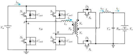
Figure 1.
Main power stage.
Before proceeding to the explanation of the proposed structure exchange, the following definitions and assumptions are given:
- (1)
- Vin, Vo, iin, and io are the input voltage, the output voltage, the input current, and the output current, respectively;
- (2)
- VAB is the voltage across the primary transformer;
- (3)
- Ip is the current of the primary transformer;
- (4)
- iLo is the current of the output inductor;
- (5)
- Ts is the switching period, and fs is the switching frequency;
- (6)
- D and Deff denote the duty cycle and the effective duty cycle, respectively;
- (7)
- Np and Ns represent the number of coils on the primary side and the number of coils on the secondary side, respectively;
- (8)
- The output capacitances of the power switches, called Coss1, Coss2, Coss3, and Coss4, are all equal;
- (9)
- The output capacitances are not considered for the secondary-side power switches;
- (10)
- Since the resonant time is comparatively short, the resonant current can be considered linear as a result.
2.2. FBPSS Transferred to Two-Switch Forward Structure (TSFS)
This section describes the process of converting the FBPSS transferred to the TSFS. Figure 2 shows its key waveforms.
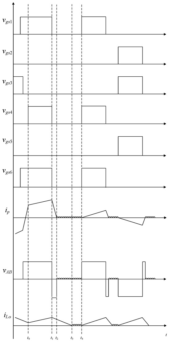
Figure 2.
Key waveforms for FBPSS transferred to TSFS.
State 1 [t0 ≤ t ≤ t1]: In this state, the switches S1, S4, and S6 are on, and the voltage across terminals A and B is vAB is Vin. Figure 3 shows the current flow in this state for FBPSS transferred to TSFS. From Figure 3, one can see that the resonant inductor Lr and the magnetizing inductance of the main transformer are magnetized, while the main transformer transfers energy to the secondary side, and the output inductor Lo is magnetized. In addition, the secondary-side diode D5 is cut off due to reverse bias, and the secondary-side current flows through the switch S6, the output inductor Lo, and the output capacitor Co to form a current loop. Until t1, the switches S1, S4, and S6 are cut off, and the circuit enters the next state.
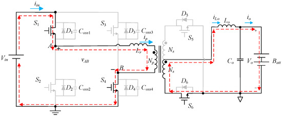
Figure 3.
Current flow in state 1 for FBPSS transferred to TSFS.
State 2 [t1 ≤ t ≤ t2]: As shown in Figure 4, the switches S1, S4, and S6 are cut off. As a result, the voltage across terminals A and B is vAB is −Vin. During this state, the resonant inductor Lr and the magnetizing inductance of the main transformer are demagnetized, and the main transformer transfers energy to the secondary side through the body diodes D2 and D3. At the same time, not only the secondary-side body diode D6 conducts due to the continuous current of the output inductor Lo but also the secondary-side body diode D5 due to the reverse bias. Until the resonant inductor Lr is fully demagnetized, the circuit enters the next state.
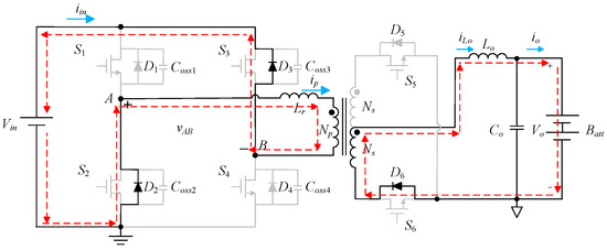
Figure 4.
Current flow in state 2 for FBPSS transferred to TSFS.
State 3 [t2 ≤ t ≤ t3]: In this state, the switches S1, S4, and S6 are still cut off, and the voltage across terminals A and B is vAB is zero. Figure 5 shows the current flow in state 3 for FBPSS transferred to TSFS. During this state, not only the resonant inductor Lr has been fully demagnetized but also the output inductor Lo continues to be demagnetized. At the same time, since there is no voltage across the primary side of the transformer, the secondary-side current ip flows through the output inductor Lo, the output capacitor Co, and the body diodes D5 and D6 to form a current loop.
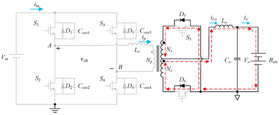
Figure 5.
Current flow in state 3 for FBPSS transferred to TSFS.
State 4 [t3 ≤ t ≤ t4]: As shown in Figure 6, the switches S1, S4, and S6 are still cut off, and the voltage between terminals A and B is vAB is zero. During this state, the output inductor Lo has been fully demagnetized, and the energy of load is provided by the output capacitor Co. After this state, the circuit enters the two-transistor forward structure.
Figure 6.
Current flow in state 4 for FBPSS transferred to TSFS.
2.3. TSFS Transferred to FBPSS
This section describes the process of converting the TSFS transferred to the FBPSS. Figure 7 shows its key waveforms.
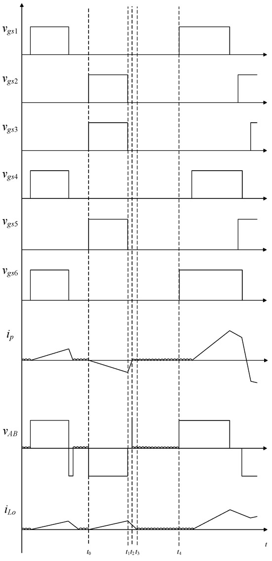
Figure 7.
Illustrated waveforms for TSFS transferred to FBPSS.
State 1 [t0 ≤ t ≤ t1]: As shown in Figure 8, the switches S2, S3, and S5 are on, and the voltage across terminals A and B is vAB is −Vin. From Figure 8, one can know that the resonant inductor Lr and the magnetizing inductance of the main transformer are demagnetized in the opposite direction, while the energy of the main transformer is transferred to the secondary side and the output inductor Lo is magnetized. At the same time, the secondary-side current flows through the output inductor Lo, the output capacitor Co, and the switch S5 to form a current loop.
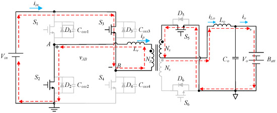
Figure 8.
Current flow in state 1 for TSFS transferred to FBPSS.
State 2 [t1 ≤ t ≤ t2]: As shown in Figure 9, S2, S3, and S5 are still cut off, and the voltage across terminals A and B is vAB is −Vin. During this state, the resonant inductor Lr and the magnetizing inductance of the main transformer are magnetized in the opposite direction, and the main transformer transfers energy to the secondary side through the body diodes D1 and D4. At the same time, the secondary-side body diode D5 conducts due to the continuous current of the output inductor Lo, and the secondary-side body diode D6 cuts off due to the reverse bias. Until the current in the resonant inductor Lr is zero, the circuit enters the next state. The equations of the voltage vAB and the currents iLo and ip are shown below.
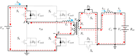
Figure 9.
Current flow in state 2 for TSFS transferred to FBPSS.
State 3 [t2 ≤ t ≤ t3]: As shown in Figure 10, the switches S2, S3, and S5 are still cut off, and the voltage across terminals A and B is vAB is zero. Simultaneously, the secondary-side current flows through the output inductor Lo, the output capacitor Co, and the body diodes D5 and D6 to form a current loop.
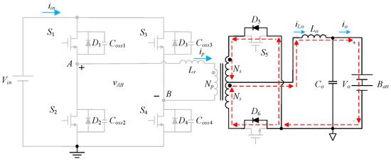
Figure 10.
Current flow is state 3 for TSFS transferred to FBPSS.
State 4 [t3 ≤ t ≤ t4]: As shown in Figure 11, the switches S1, S4, and S6 are still cut off, and the voltage across terminals A and B is vAB is zero. During this state, the current in the output inductor Lo is zero, and the energy needed by the load is provided by the output capacitor Co. After this state, the circuit enters the full-bridge phase-shift structure.
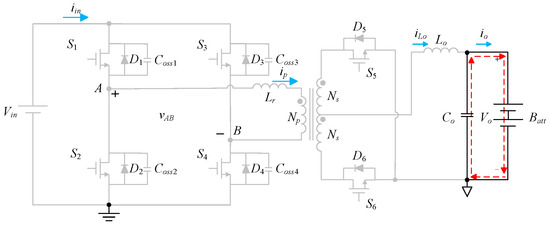
Figure 11.
Current flow is state 4 for TSFS transferred to FBPSS.
3. Design Considerations
This section describes the circuit design, including the given system specifications and the component specifications used.
3.1. System Configuration
Figure 12 shows the proposed system configuration, which consists of two types of circuits: the main circuit and the feedback control circuit. As shown in Figure 12, the main circuit is a full-bridge phase-shift circuit with synchronous rectification. In terms of the feedback control circuit, a current sensor and a voltage divider are used to detect the output voltage and current signals, which are then sent to the analog-to-digital converter (ADC 0 and ADC 1) inside the digital signal processor (DSP) to obtain the individual digital signals, and then the corresponding control forces are obtained by the algorithm to generate PWM signals to regulate the power switches so as to obtain the required output voltage and current.
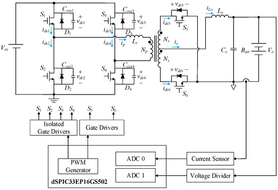
Figure 12.
System configuration.
3.2. System Specifications
Table 2 shows the system specifications, from which the required main component parameters of the circuit can be designed and summarized in Table 3.
Table 2.
System specifications.
Table 3.
Component specifications used.
3.3. Design of Resonant Capacitor and Inductor
In order to achieve ZVS of the power switches on the primary side, the resonant inductor should resonate with the parasitic capacitance, and the energy should be large enough to convince the power switches to zero before they turn on to complete ZVS.
where Cr is the sum of the parasitic capacitance of the power switch, Coss, and the stray capacitance of the transformer XFMR, CXFMR.
Accordingly, the resonant capacitor Cr can be expressed as
Since the value of Coss can be obtained to be 176 pF from the corresponding datasheet, and the value of CXFMR can be measured to be about 136 pF, substituting these values into (2) yields
From (1), it can be seen that the resonance condition depends on the current Ip. Since the value of Ip is set at 30% of the load current, the corresponding value is
Substituting (3) and (4) into (1) yields
The value of the resonant inductor Lr includes the primary-side leakage inductance Llk and the required external resonant inductance Lext. Since the value of Llk can be measured to be 12.2 µH, the required primary-side external resonant inductance Lext can be calculated to be
4. Control Program Flowchart
In this paper, a DSP is used as the control kernel, whose model name is dsPIC33EP16GS502, manufactured by Microchip Technology Inc. (Chandler, AZ, USA), and the C language is used to realize the required functions. The dsPIC33EP16GS502 has a 7.37 MHz oscillator, four high-speed PWMs, 12-bit analog-to-digital converters, a 12-bit digital-to-analog converter, flash memory of 16 kB, and 2 kB of random-access memory (RAM).
4.1. Main Program Flowchart
The main program flowchart is shown in Figure 13. The analog signals are sampled by triggering the analog-to-digital converters ADC0 and ADC1, converted to digital data, and then the errors are generated by subtracting these digital data from the target values and sent to the PI control module to obtain the required control forces that are sent the PWM module to obtain the corresponding gate-driving signals for the switches.
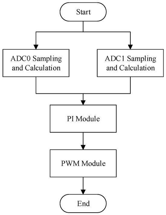
Figure 13.
Main program flowchart [34].
4.2. ADC Module
Figure 14 shows the flowchart of ADC. The ADC0 sampling and calculation and the ADC1 sampling and calculation are responsible for sampling the output voltage Vo and the output current Io, respectively, which are triggered by the PWM1 signal to achieve the sampling purpose. After this, subtracting the voltage feedback signal vfb and the current feedback signal ifb from the voltage command vref and the current command iref, respectively, yields the error values VError and IError, which are finally sent to the PI module.
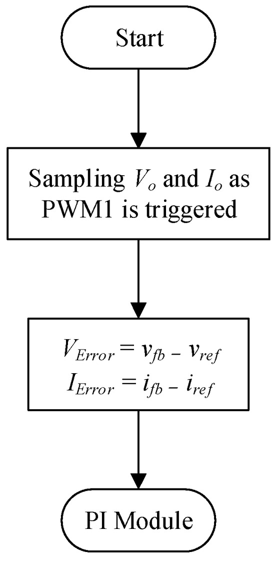
Figure 14.
ADC flowchart [34].
In order for the converter output voltage and current signals to be input to the digital controller, these signals need to be processed by the ADC module to convert them to digital signals. This DSP has a built-in 12-bit ADC, whose value is from 0 to 4095 in the decimal system. Since the acceptable voltage range of the ADC is 3.3 V, the output voltage and current commands are given in (7) and (8) as follows:
4.3. PI Module
Figure 15 shows the flowchart of the PI module, in which there are two gains of P (proportional gain) and I (integral gain) to control the output voltage and current, respectively. The proportional control forces Pv and Pi can be ob99++tained by multiplying the resulting voltage error VError and current error IError by the coefficients Vkp and Ikp, respectively. The integral control forces Iv and Ii can be obtained by multiplying the resulting voltage error VError and current error IError by the coefficients Vki and Iki, respectively, and adding with the previous integral control forces. Eventually, the voltage control force CFv can be obtained by adding Pv and Iv, whereas the current control force CFi can be obtained by adding Pi and Ii. Under constant current control, the full-bridge phase-shifted topology will be operated, and the current control force will be used to regulate the phase. Under constant-voltage control, the current is detected, and if this detected current is above the switching point value, the system will operate in the full-bridge phase-shift structure, with the phase regulated by the voltage control force. Conversely, if the detected current is below the switching point value, the system will operate in the two-transistor structure, and the voltage control force is used to regulate the duty cycle. In order to prevent the system from going out of control, it is necessary to add the minimum control force and the maximum control force to limit the duty cycle, and finally, the resulting control force is fed into the PWM module.
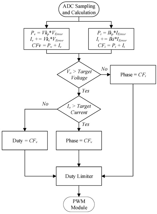
Figure 15.
PI flowchart [34].
4.4. PWM Module
The PWM of the DSP is 16-bit, and the PWM control is realized by setting the PWM-related registers. The related registers are duty cycle, frequency, phase, blanking time, complementary relationship, etc., which can be set so the value of the control force CF can be directly fed into the registers related to the duty cycle. The full-bridge phase-shift structure requires three PWMs, and one PWM has two PWM outputs; the signal of the front leg is generated by PWM1, the signal of the rear leg is generated by PWM2, and the signal of the SR is generated by PWM3. The frequencies of PWM1, PWM2, and PWM3 are set to 100 kHz, and the blanking times are set to 300 ns to avoid damage to the switches due to turn-on of the switches on the same leg.
5. Experimental Results
To verify the parameters of the circuit shown in Table 2 and Table 3, an electronics load (3255, Prodigit Electronics Co., Ltd., Taiwan) and a DC power supply (PSW80-27, GW Instek., Taiwan) will be used to provide the load input and voltage. As a result, one can measure the waveforms, and afterward, the measured waveforms will be explained.
5.1. Measured Waveforms Under Constant Current at 40 V and 17 A for FBPSS
Figure 16 shows the waveforms of gate-driving signals vgs1 for switch S1, vgs2 for S2, vgs3 for switch S3, and vgs4 for switch S4. Figure 17 shows the waveforms of the gate-driving signals vgs1 for switch S1, vgs4 for switch S4, and vgs6 for switch S6. Figure 18 shows the gate-driving signals vgs2 for switch S2, vgs3 for switch S3, and vgs5 for switch S5. Figure 19 shows the waveforms of the primary-side voltage between points A and B, called vAB, primary-side current ip, the output voltage Vo, and the output current Io. Figure 20 shows the waveforms of the gate-driving signal vgs1 for switch S1 and the voltage vds1 for switch S1. Figure 21 shows the waveforms of the gate-driving signal vgs2 for switch S2 and the voltage vds2 for switch S2. Figure 22 shows the waveforms of the gate-driving signal vgs3 for switch S3 and the voltage vds3 for switch S3. Figure 23 shows the gate-driving signal vgs4 for switch S4 and the voltage vds4 for switch S4. From Figure 16, Figure 17, Figure 18, Figure 19, Figure 20, Figure 21, Figure 22 and Figure 23, one can see that all switches at rated load have ZVS turn-on.
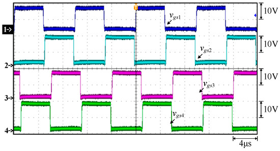
Figure 16.
Measured waveforms under constant current at 40 V and 17 A for FBPSS: (1) vgs1; (2) vgs2; (3) vgs3; (4) vgs4.
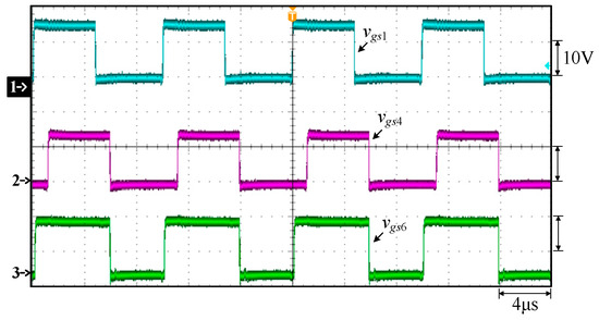
Figure 17.
Measured waveforms under constant current at 40 V and 17 A for FBPSS: (1) vgs1; (2) vgs4; (3) vgs6.
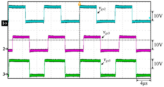
Figure 18.
Measured waveforms under constant current at 40 V and 17 A for FBPSS: (1) vgs2; (2) vgs3; (3) vgs5.
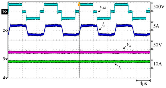
Figure 19.
Measured waveforms under constant current at 40 V and 17 A for FBPSS: (1) vAB; (2) ip; (3) Vo; (4) Io.
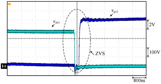
Figure 20.
Measured waveforms under constant current at 40 V and 17 A for FBPSS: (1) vgs1; (2) vds1.
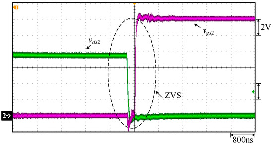
Figure 21.
Measured waveforms under constant current at 40 V and 17 A for FBPSS: (1) vgs2; (2) vds2.
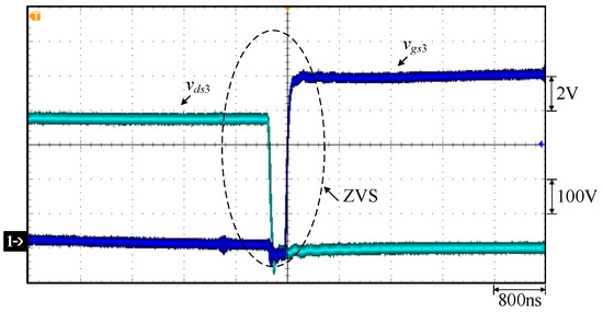
Figure 22.
Measured waveforms under constant current at 40 V and 17 A for FBPSS: (1) vgs3; (2) vds3.
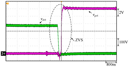
Figure 23.
Measured waveforms under constant current at 40 V and 17 A for FBPSS: (1) vgs4; (2) vds4.
5.2. Measured Waveforms Under Constant Voltage at 58.4 V and 1.7 A for TSFS
Figure 24 shows the waveforms of the gate-driving signals vgs1 for switch S1, vgs2 for S2, vgs3 for switch S3, and vgs4 for switch S4. Figure 25 shows the gate-driving signals vgs1 for switch S1, vgs4 for switch S4, and vgs6 for switch S6. Figure 26 shows the gate-driving signals vgs2 for switch S2, vgs3 for switch S3, and vgs5 for switch S5. Figure 27 shows the waveforms of the primary-side voltage between points A and B, called vAB, the output voltage Vo, the primary-side current ip, the output current Io, and the voltage vds3 for switch S3. From Figure 24, Figure 25, Figure 26 and Figure 27, one can see that when the switch is turned off, the resonant inductor resonates with the body capacitance of the switch, resulting in oscillations in the primary-side voltage and current.
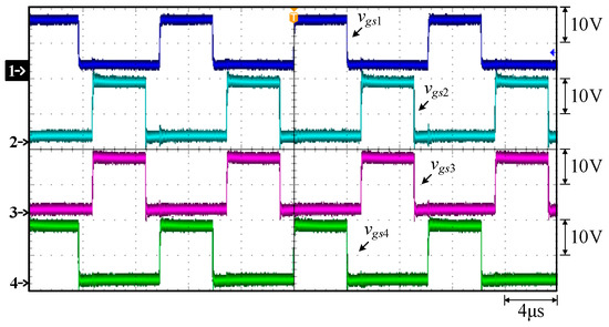
Figure 24.
Measured waveforms under constant voltage at 58.4 V and 1.7 A for TSFS: (1) vgs1; (2) vgs2; (3) vgs3; (4) vgs4.
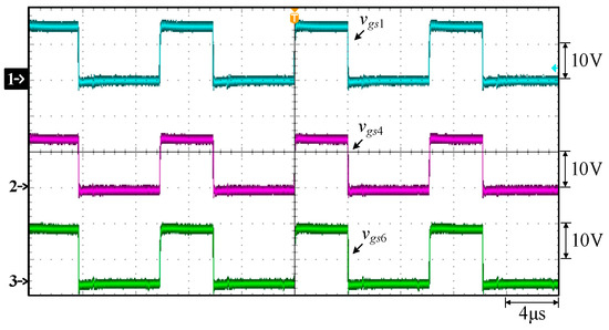
Figure 25.
Measured waveforms under constant voltage at 58.4 V and 1.7 A for TSFS: (1)vgs1; (2) vgs4; (3) vgs6.
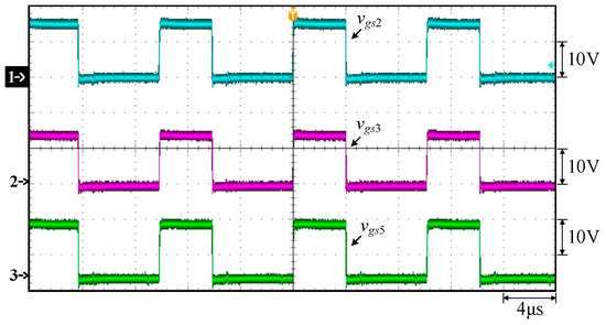
Figure 26.
Measured waveforms under constant voltage at 58.4 V and 1.7 A for TSFS: (1) vgs2; (2) vgs3; (3) vgs5.
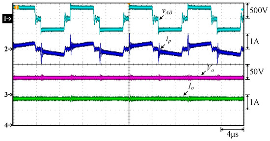
Figure 27.
Measured waveforms under constant voltage at 58.4 V and 1.7 A for TSFS: (1) vAB; (2) ip; (3) Vo; (4) Io.
5.3. Measured Waveforms for Transferring FBPSS to TSFS
Figure 28 shows the waveforms of the voltage across points A and B on the primary side, vAB, the primary-side current ip, the output voltage Vo, and the output current Io when the FBPSS is converted to the TSFS.
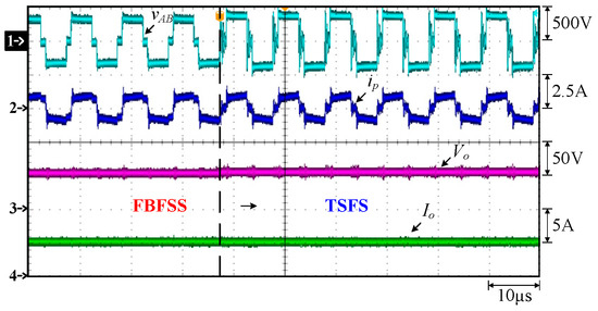
Figure 28.
Measured waveforms for transferring FBPSS to TSFS: (1) vAB; (2) ip; (3) Vo; (4) Io.
5.4. Measured Waveforms for Transferring TSFS to FBPSS
Figure 29 shows the waveforms of the voltage across points A and B on the primary side, vAB, the primary-side current ip, the output voltage Vo, and the output current Io when the TSFS is converted to the FBPSS.
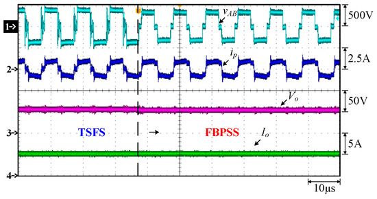
Figure 29.
Measured waveforms for transferring TSFS to FBPSS: vAB; (2) ip; (3) Vo; (4) Io.
5.5. Efficiency Measurement
In this section, the efficiency of battery charging is measured in different modes of the converter. A digital meter is adopted to measure the input and output voltages, and a current-sensing resistor is used and connected in series with the input and output current. In addition, the digital meter is not only used to measure the voltage across the current-sensing resistor to find out the values of the input and output currents but also the input and output powers. At the same time, a DC electronic load is used to simulate the behavior of the battery on the load side. Finally, the actual circuit efficiency is calculated. Figure 30 shows the curves of the efficiency measurement of the full-bridge phase-shift structure and two-switch flyback structure in constant-voltage mode. From Figure 30, one can see that the converter is switched to the two-switch forward structure under constant voltage, and the efficiency below 30% of the rated load can be improved by up to 7.1% compared to the full-bridge phase-shift structure. Figure 31 shows the curve of efficiency measurement of the full-bridge phase-shift structure under constant current. From Figure 31, it can be seen that the efficiency rises slightly as the output voltage increases.
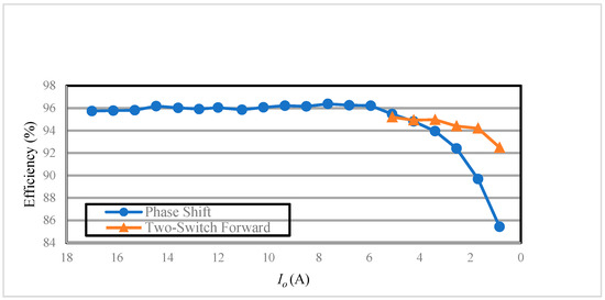
Figure 30.
Efficiency curves for phase shift and two-switch forward under constant voltage.
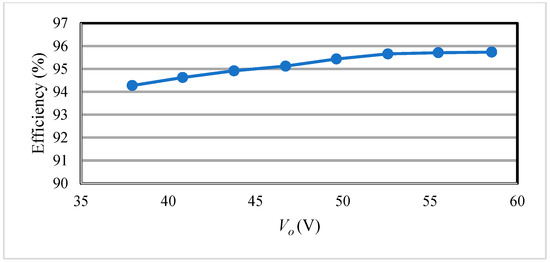
Figure 31.
Efficiency curve for phase shift under constant current.
5.6. Comparison Between the Proposed Converter and Other Topologies
Comparisons of the proposed converter with topologies operated as battery chargers [6,7,13,14,15,16,28] based on various criteria and features are presented in Table 4. From this table, the proposed converter possesses the highest light-load efficiency.
Table 4.
Comparisons between the proposed converter and existing topologies.
6. Conclusions
In this paper, a full-bridge DC–DC converter with structure exchange is applied to battery charging. The full-bridge phase-shift converter uses an external resonant inductor and phase-shift control on the primary side to achieve ZVS above medium load. However, the energy of the resonant inductor is not so enough to carry away the energy of the parasitic capacitance on the switch at light load, resulting in the inability of ZVS as well as the circulating current problem existed by the long duration of the primary-side circulating current time. Therefore, to solve these problems, the structure exchange, with only the control strategy changed from the phase-shift control to the two-switch forward control, is adopted to enhance the light-load efficiency significantly. Compared to the conventional BFPSS, the light-load efficiency of this converter can be increased by up to 7.1%.
Author Contributions
Conceptualization, K.-I.H. and J.-J.S.; Methodology, K.-I.H., P.-C.T. and J.-J.S.; Software, P.-C.T.; Validation, K.-I.H. and P.-C.T.; Formal analysis, P.-C.T.; Investigation, P.-C.T.; Resources, K.-I.H.; Data curation, P.-C.T. and J.-J.S.; Writing—original draft, K.-I.H.; Writing—review & editing, K.-I.H.; Visualization, P.-C.T. and J.-J.S.; Supervision, K.-I.H.; Project administration, K.-I.H.; Funding acquisition, K.-I.H. All authors have read and agreed to the published version of the manuscript.
Funding
This research was funded by the Ministry of Science and Technology, Taiwan, under Grant Number NSTC 112-2221-E-027-015-MY2.
Data Availability Statement
The original contributions presented in the study are included in the article, further inquiries can be directed to the corresponding author.
Conflicts of Interest
The authors declare no conflict of interest.
References
- Noh, G.; Lee, J.; Ha, J.-I. Design and analysis of single-inductor power converter for both battery balancing and voltage regulation. IEEE Trans. Ind. Electron. 2022, 69, 2874–2884. [Google Scholar] [CrossRef]
- Deng, R.; Liu, Y.; Chen, W.; Liang, H. A survey on electric buses-energy storage, power management, and charging scheduling. IEEE Trans. Intell. Transp. Syst. 2021, 22, 9–22. [Google Scholar] [CrossRef]
- Rahman, M.S.; Rahman, S.F.; Rahman, M.A.; Al Mansur, A. Advancements and Challenges in Electric Vehicle Battery Technology and Charging Solutions: Towards a Sustainable Transportation. In Proceedings of the 6th International Conference on Sustainable Technologies for Industry 5.0 (STI), Dhaka, Bangladesh, 14–15 December 2024; pp. 1–5. [Google Scholar]
- King, B. Selecting Optimal Topology. TI, 2017. Available online: https://www.ti.com/content/dam/videos/external-videos/en-us/2/3816841626001/5589612393001.mp4/subassets/Selecting-Optimal-Topology.pdf (accessed on 17 January 2023).
- Lee, F.C. High-frequency quasi-resonant and multi-resonant converter technologies. In Proceedings of the 14 Annual Conference of Industrial Electronics Society, Singapore, 24–28 October 1988; pp. 509–521. [Google Scholar]
- Phetphimoon, W.; Bhumkittipich, K.; Prabpal, P.; Yupapin, P.; Kongjeen, Y. Phase-shifted full-bridge zvs dc-dc converter with synchronous double rectifiers for battery charging applications. Int. Trans. Electr. Energy Syst. 2022, 2022, 1–12. [Google Scholar] [CrossRef]
- Wang, X.; Zhao, Q.; Zhao, Z.; Meng, F. Full-bridge dc-dc converter with synchronous rectification based on GaN transistors. J. Low Power Electron. Appl. 2025, 15, 25. [Google Scholar] [CrossRef]
- Gautam, K.K.; Chatterjee, A.; Prasad, D. Inherent constant current constant voltage (CCCV) charging of electric vehicles by using lcl resonant converter. In Proceedings of the 2nd International Conference for Innovation in Technology (INOCON), Bangalore, India, 10–12 March 2023; pp. 1–6. [Google Scholar]
- Di, Z.; Donglai, Z.; Zicai, W.; Hua, Z.; Ying, Z. Current-sharing active-clamped forward power converter with self-driven synchronous rectifier. In Proceedings of the IEEE 3rd International Conference on Electronics Technology (ICET), Chengdu, China, 8–11 May 2020; pp. 334–338. [Google Scholar]
- Wang, J.; Lu, B. Open loop synchronous rectifier driver for LLC resonant converter. In Proceedings of the IEEE Applied Power Electronics Conference and Exposition (APEC), Long Beach, CA, USA, 17–21 March 2013; pp. 2048–2051. [Google Scholar]
- Ho, G.K.Y.; Yu, R.; Pong, B.M.H. Current driven synchronous rectifier for LLC resonant converter with a novel integrated current transformer. In Proceedings of the IET International Conference on Power Electronics, Machines and Drives (PEMD 2012), Bristol, UK, 27–29 March 2012; pp. 1–5. [Google Scholar]
- Fei, C.; Li, Q.; Lee, F.C. Digital implementation of adaptive synchronous rectifier driving scheme for high-frequency LLC converters with microcontroller. IEEE Trans. Power Electron. 2018, 33, 5351–5361. [Google Scholar] [CrossRef]
- López-Santos, O.; Zambrano-Prada, D.A.; Valderrama-Blavi, H.; Flores-Bahamonde, F.; Pinzón, C.A.T.; Martínez-Salamero, L. Experimental efficiency comparison between the llc resonant converter and the phase shifted full bridge converter operating as battery chargers. In Proceedings of the 50th Annual Conference of the IEEE Industrial Electronics Society (IECON), Chicago, IL, USA, 20–23 October 2024; pp. 1–6. [Google Scholar]
- Werulkar, A.S.; Kulkarni, P.S. Efficiency improvement of a dual boost converter with zero voltage switching technique for battery charging application of a solar home lighting system. In Proceedings of the IEEE First International Conference on Smart Technologies for Power, Energy and Control (STPEC), Nagpur, India, 25–26 September 2020; pp. 1–6. [Google Scholar]
- Geda, M.G.; Song, H.; Do, B.P.; Choi, S. Light load efficiency enhancement strategy for single-stage ac-dc by using adaptive switching frequency. In Proceedings of the IEEE 10th International Power Electronics and Motion Control Conference (IPEMC2024-ECCE Asia), Kitakyushu, Japan, 12–15 May 2024; pp. 1–5. [Google Scholar]
- Lu, Y.; Wu, H.; Dong, X.; Xing, Y. Light load efficiency improvement for distributed battery energy storage system. In Proceedings of the 42nd Annual Conference of the IEEE Industrial Electronics Society (IECON), Florence, Italy, 23–26 October 2016; pp. 1–5. [Google Scholar]
- Dhiman, S.; Vasudevan, K. Optimal design of battery charging converters based on energy efficiency. In Proceedings of the IEEE 12th Energy Conversion Congress & Exposition-Asia (ECCE-Asia), Singapore, 24–27 May 2021; pp. 1–6. [Google Scholar]
- Sharma, D.K.; B K Vardhan, H.; Hulipalled, V.R. EV home charging infrastructure & low battery AI algorithm. In Proceedings of the Third International Conference on Smart Technologies in Computing, Electrical and Electronics (ICSTCEE), Bengaluru, India, 16–17 December 2022; pp. 1–9. [Google Scholar]
- Rakshith, S.K.; Rohit, S.; Sutha, S.; Goyal, H.R. Smart energy: Artificial intelligence (AI) in charging and battery management systems. In Proceedings of the 5th International Conference on Intelligent Communication Technologies and Virtual Mobile Networks (ICICV), Tirunelveli, India, 4–6 January 2024; pp. 68–73. [Google Scholar]
- KS, K.K.; Chitra, L.; Abraham, J.M.; Joseph, N.; TK, Y.K. The role of IOT & AI in battery management of electric vehicles. In Proceedings of the International Conference on Signal Processing, Computation, Electronics, Power and Telecommunication (IConSCEPT), Kollam, India, 8–9 March 2023; pp. 1–7. [Google Scholar]
- Tran, D.; Vu, H.; Yu, S.; Choi, W. A novel soft-switching full-bridge converter with a combination of a secondary switch and a nondissipative snubber. IEEE Trans. Power Electron. 2018, 33, 1440–1452. [Google Scholar] [CrossRef]
- Lim, C.; Han, J.; Park, M.; Kim, K.; Moon, G. Phase-shifted full-bridge DC-DC converter with high efficiency and reduced output filter using center-tapped clamp circuit. In Proceedings of the IEEE Applied Power Electronics Conference and Exposition (APEC), Anaheim, CA, USA, 17–21 March 2019; pp. 1710–1715. [Google Scholar]
- Lim, C.; Jeong, Y.; Lee, M.; Yi, K.; Moon, G. Half-bridge integrated phase-shifted full-bridge converter with high efficiency using center-tapped clamp circuit for battery charging systems in electric vehicles. IEEE Trans. Power Electron. 2020, 35, 4934–4945. [Google Scholar] [CrossRef]
- Lee, I.; Moon, G. Phase-shifted PWM converter with a wide ZVS range and reduced circulating current. IEEE Trans. Power Electron. 2013, 28, 908–919. [Google Scholar] [CrossRef]
- Kim, Y.-D.; Cho, K.-M.; Kim, D.-Y.; Moon, G.-W. Wide-range ZVS phase-shift full-bridge converter with reduced conduction loss caused by circulating current. IEEE Trans. Power Electron. 2013, 28, 3308–3316. [Google Scholar] [CrossRef]
- Kim, D.; Kim, C.; Moon, G. Variable delay time method in the phase-shifted full-bridge converter for reduced power consumption under light load conditions. IEEE Trans. Power Electron. 2013, 28, 5120–5127. [Google Scholar] [CrossRef]
- Liu, B.H.; Teng, J.H.; Lin, M.Y.; Huang, C.C. Light-load conversion efficiency improvement strategy for phase-shift full-bridge converters. In Proceedings of the IEEE International Future Energy Electronics Conference and ECCE Asia (IFEEC 2017-ECCE Asia), Kaohsiung, Taiwan, 3–7 June 2017; pp. 488–493. [Google Scholar]
- Sun, L.; Zhang, X.; Liu, B.; Wang, S.; Wang, Y.; Xu, D. Efficiency optimization of phase-shift full-bridge through adaptive dead-time and burst-mode at very light load. In Proceedings of the International Conference on Electrical Machines and Systems (ICEMS), Harbin, China, 11–14 August 2019; pp. 1–5. [Google Scholar]
- Arabsalmanabadi, B.; Tashakor, N.; Javadi, A.; Al-Haddad, K. Charging techniques in Lithium-ion battery charger: Review and new solution. In Proceedings of the 44th Annual Conference of the IEEE Industrial Electronics Society (IECON), Washington, DC, USA, 21–23 October 2018; pp. 5731–5738. [Google Scholar]
- Lan, Z.; Li, Y.; Gao, F.; Qiao, F. Research and implementation of step high voltage constant current closed-loop pre-charging technology. In Proceedings of the Advanced Electronic Materials, Computers and Software Engineering (AEMCSE), Changsha, China, 24–26 April 2020; pp. 810–815. [Google Scholar]
- Wang, S.; Liu, Y.; Wang, X. Resonant converter for battery charging applications with CC/CV output profiles. IEEE Access 2020, 8, 54879–54886. [Google Scholar] [CrossRef]
- Sun, T.-W.; Tsai, T.-H. A battery management system using interleaved pulse charging with charge and temperature balancing based on NARX network. IEEE Trans. Circuits Syst. I Regul. Pap. 2022, 69, 1811–1819. [Google Scholar] [CrossRef]
- Ahmadi, F.; Adib, E.; Azari, M. Soft switching bidirectional converter for reflex charger with minimum switches. IEEE Trans. Ind. Electron. 2020, 67, 8355–8362. [Google Scholar] [CrossRef]
- Lee, Y.-L.; Chen, H.-H.; Hwu, K.-I. Applying a current sharing method based on partial energy processing to multiphase LLC resonant converters. Energies 2024, 17, 3859. [Google Scholar] [CrossRef]
Disclaimer/Publisher’s Note: The statements, opinions and data contained in all publications are solely those of the individual author(s) and contributor(s) and not of MDPI and/or the editor(s). MDPI and/or the editor(s) disclaim responsibility for any injury to people or property resulting from any ideas, methods, instructions or products referred to in the content. |
© 2025 by the authors. Licensee MDPI, Basel, Switzerland. This article is an open access article distributed under the terms and conditions of the Creative Commons Attribution (CC BY) license (https://creativecommons.org/licenses/by/4.0/).