

Parameter Estimation-Based Output Voltage or Current Regulation for Double-LCC Hybrid Topology in Wireless Power Transfer Systems

 , , , and
Abstract
1. Introduction
2. Project Analysis
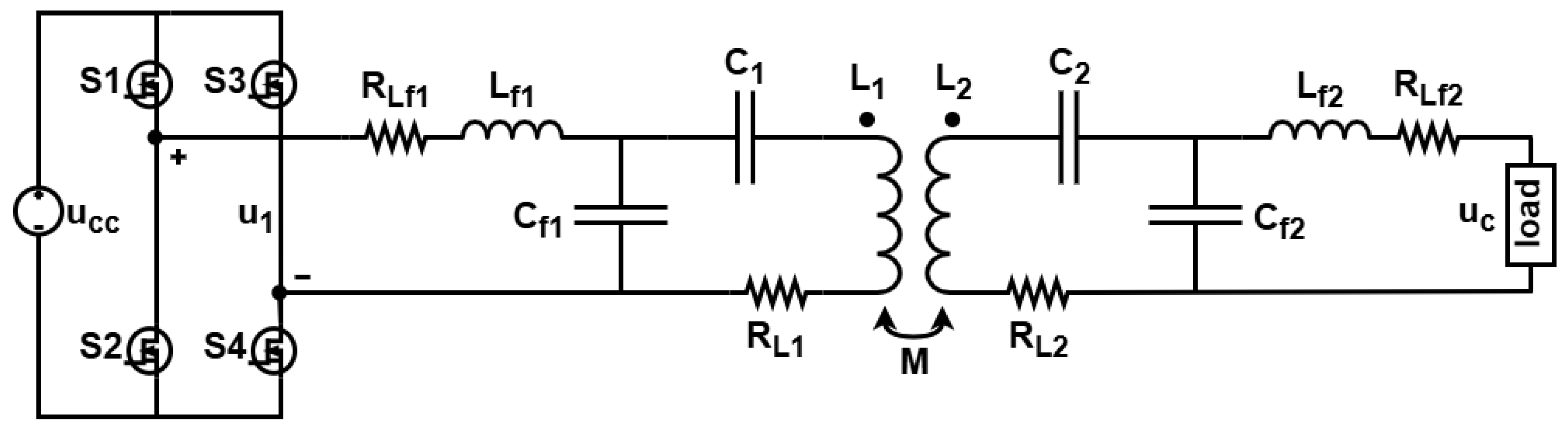
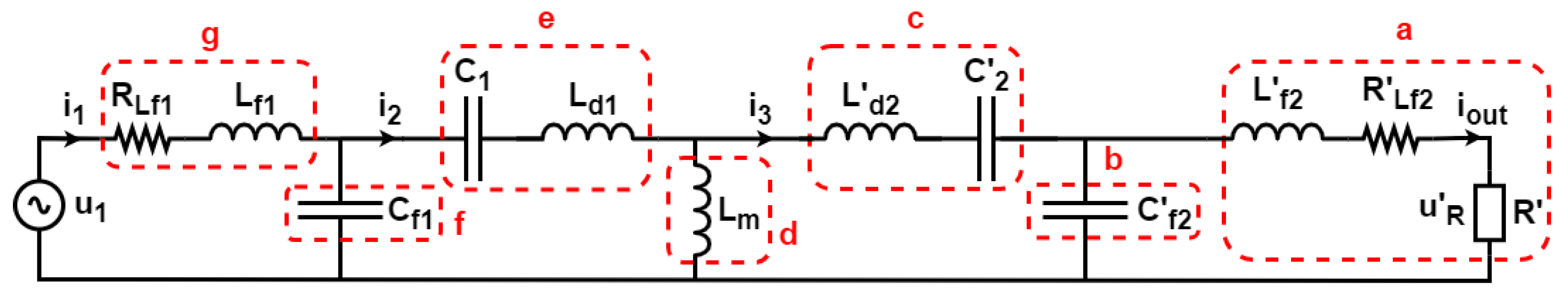
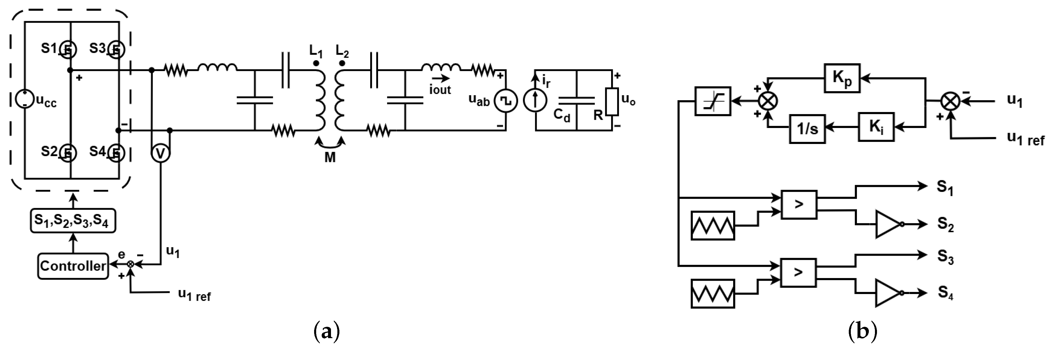
2.1. Principles
2.2. Coupling Coil Design
| Algorithm 1 Pseudo-algorithm for physical coil design. |
|
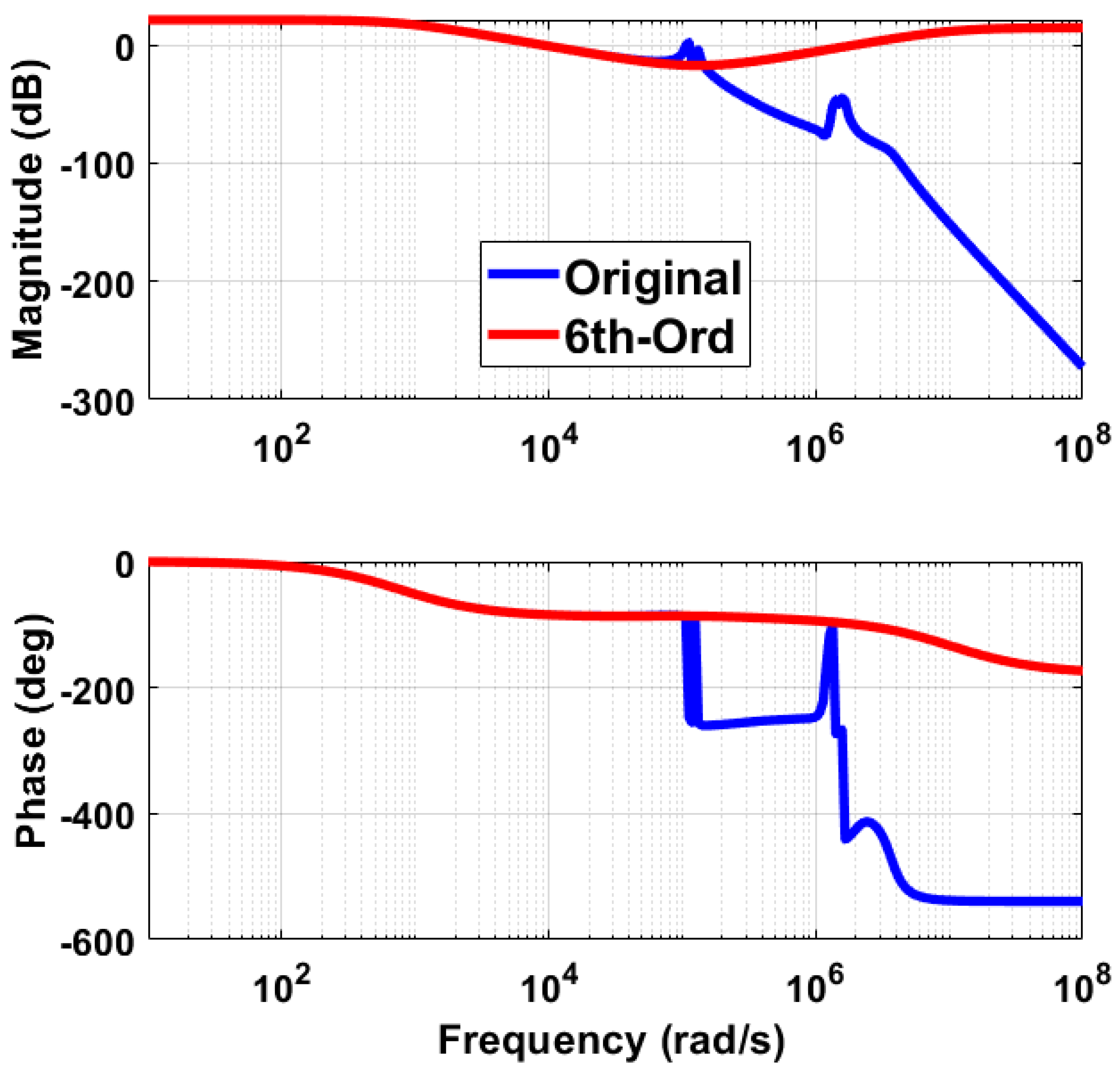
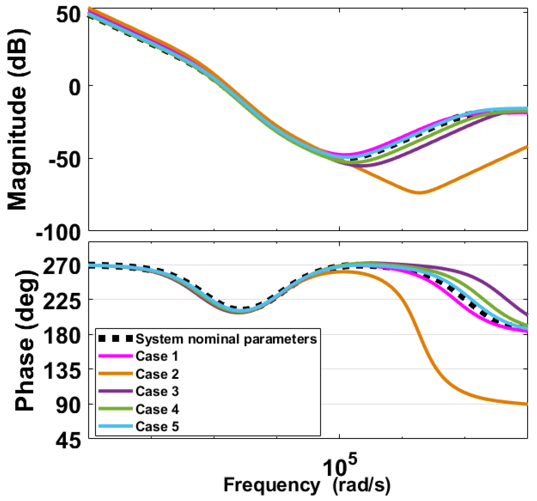
2.3. Load Estimation
2.4. Output Voltage Control
3. Simulation Results and Discussion
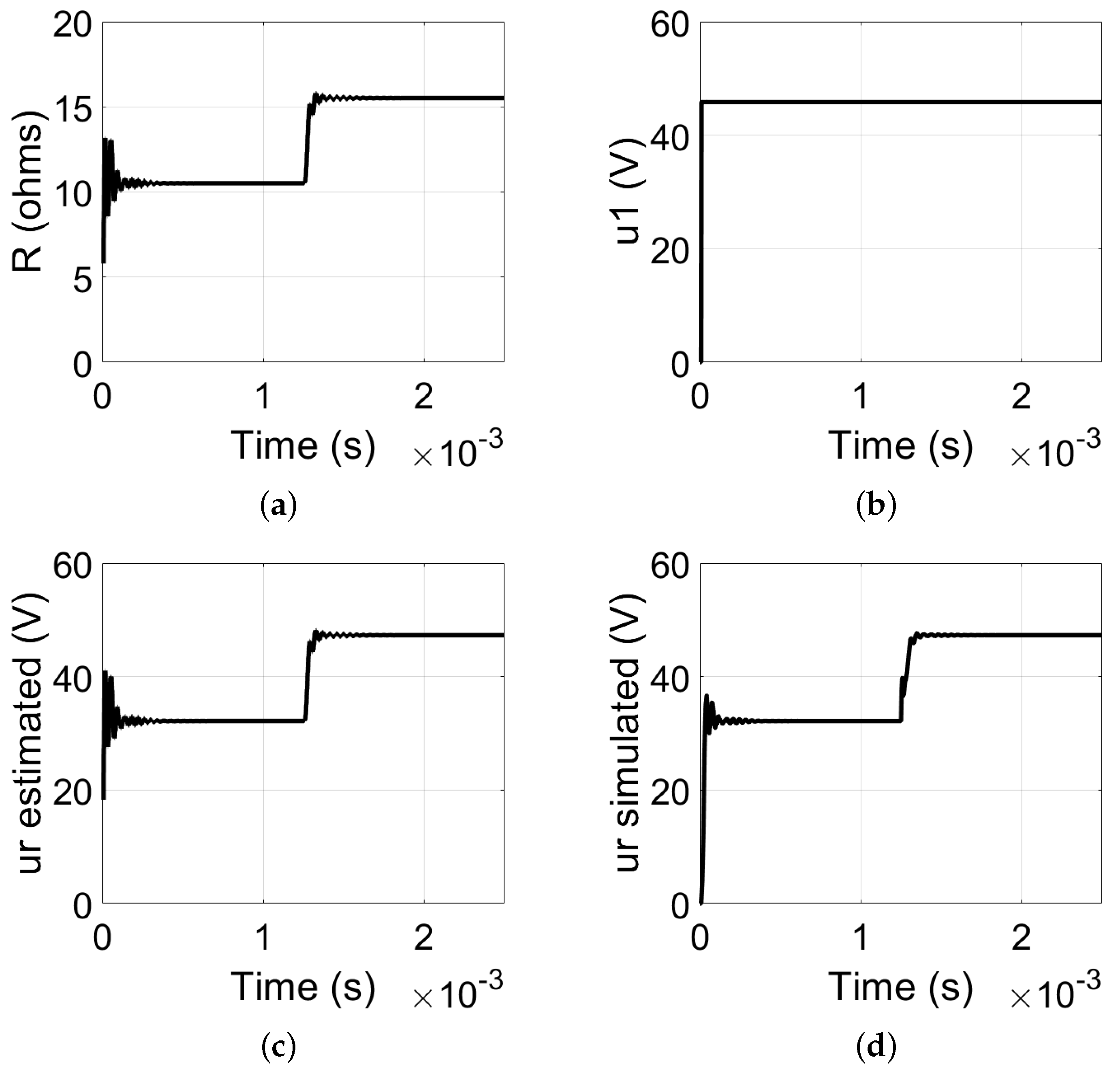
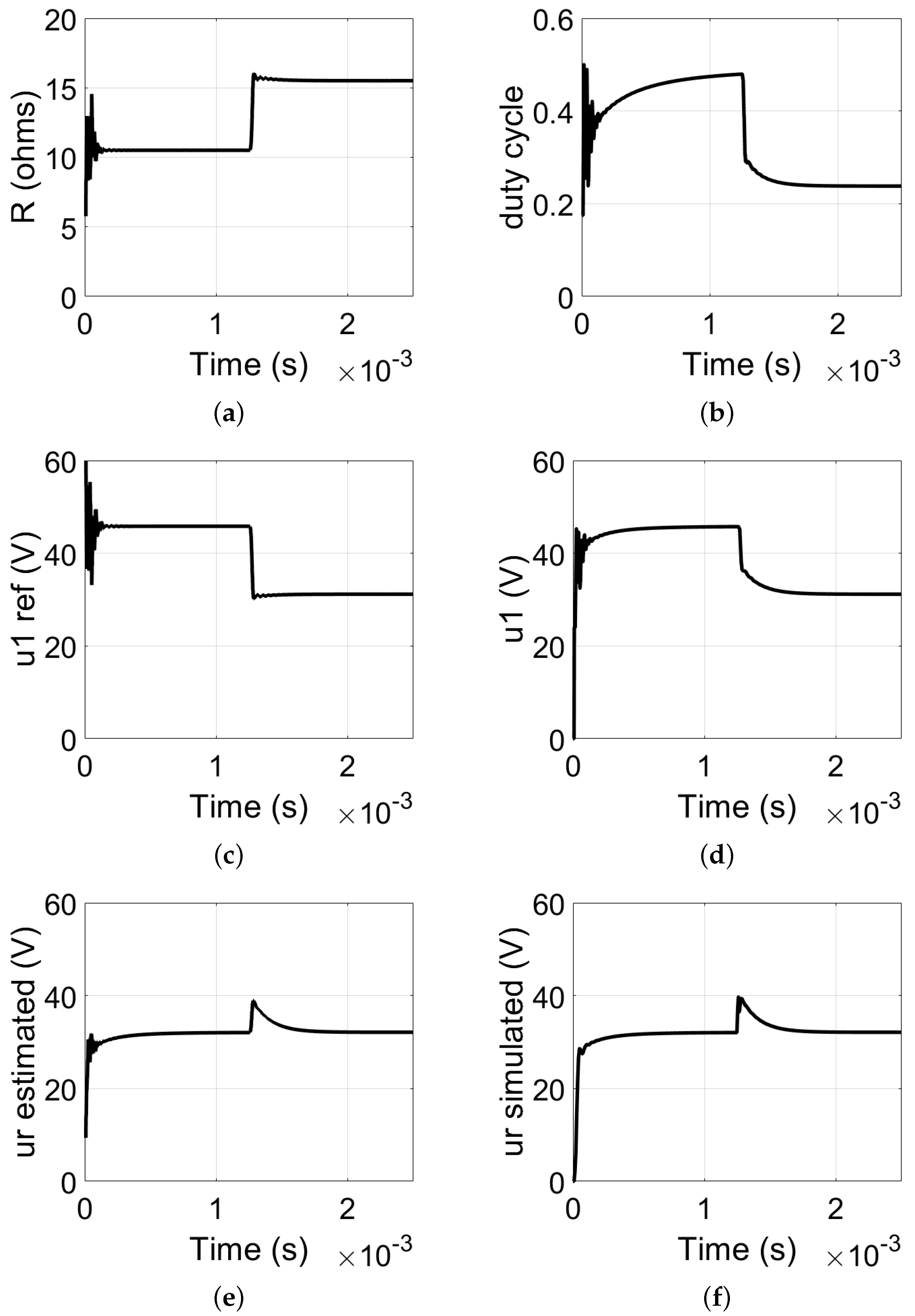
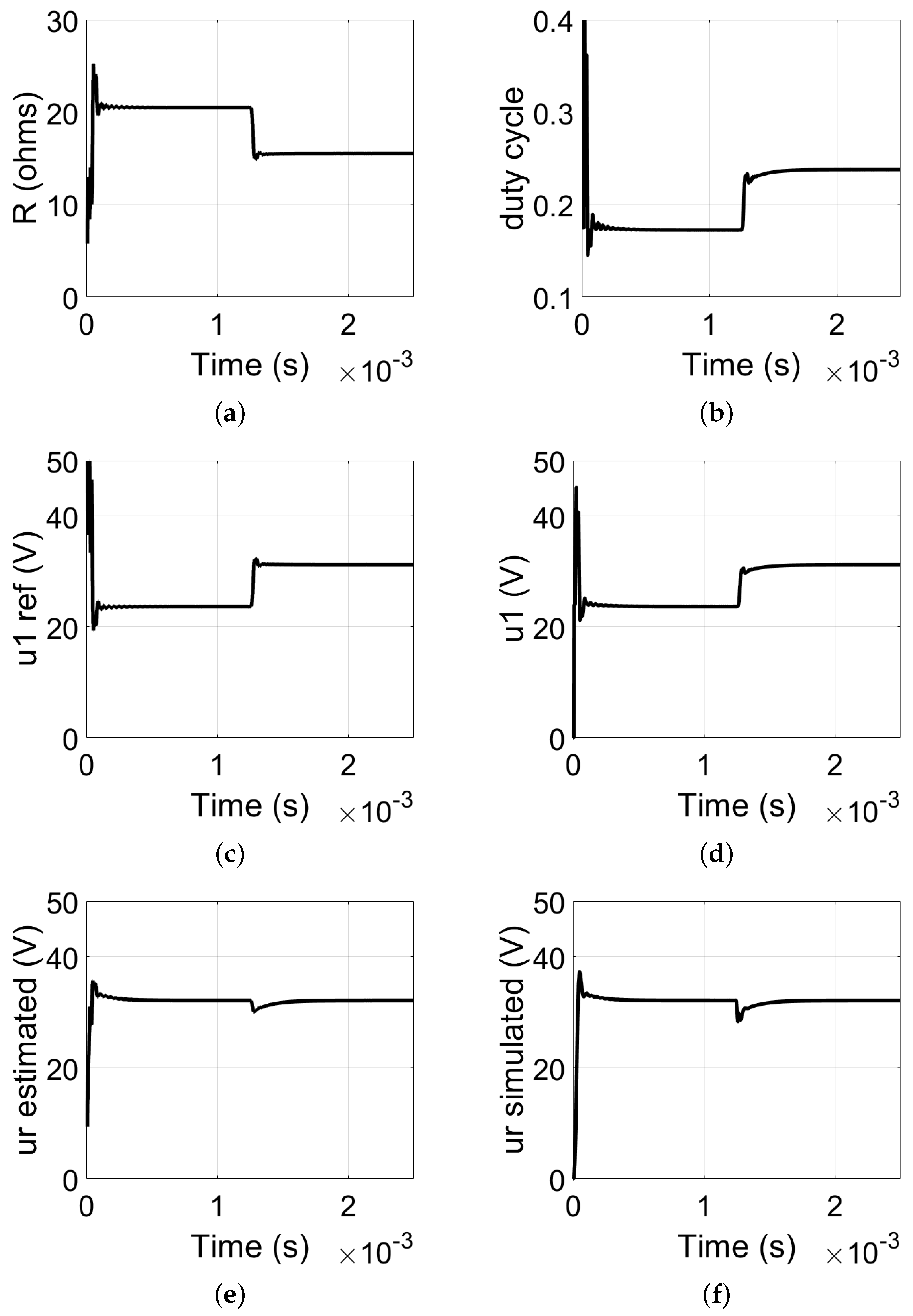
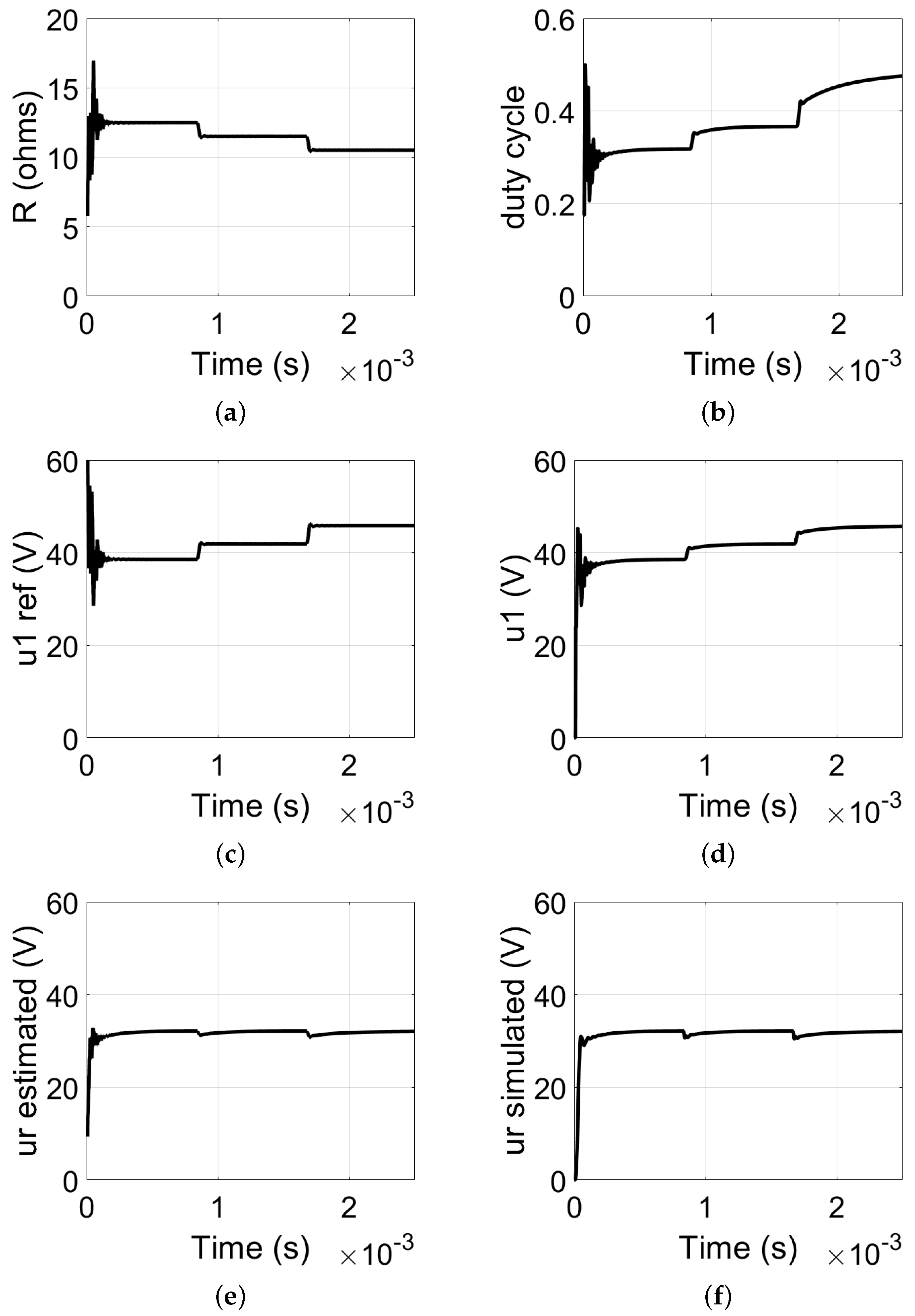
3.1. Voltage Source Operation
3.1.1. Load Step-Up
3.1.2. Load Step-Down
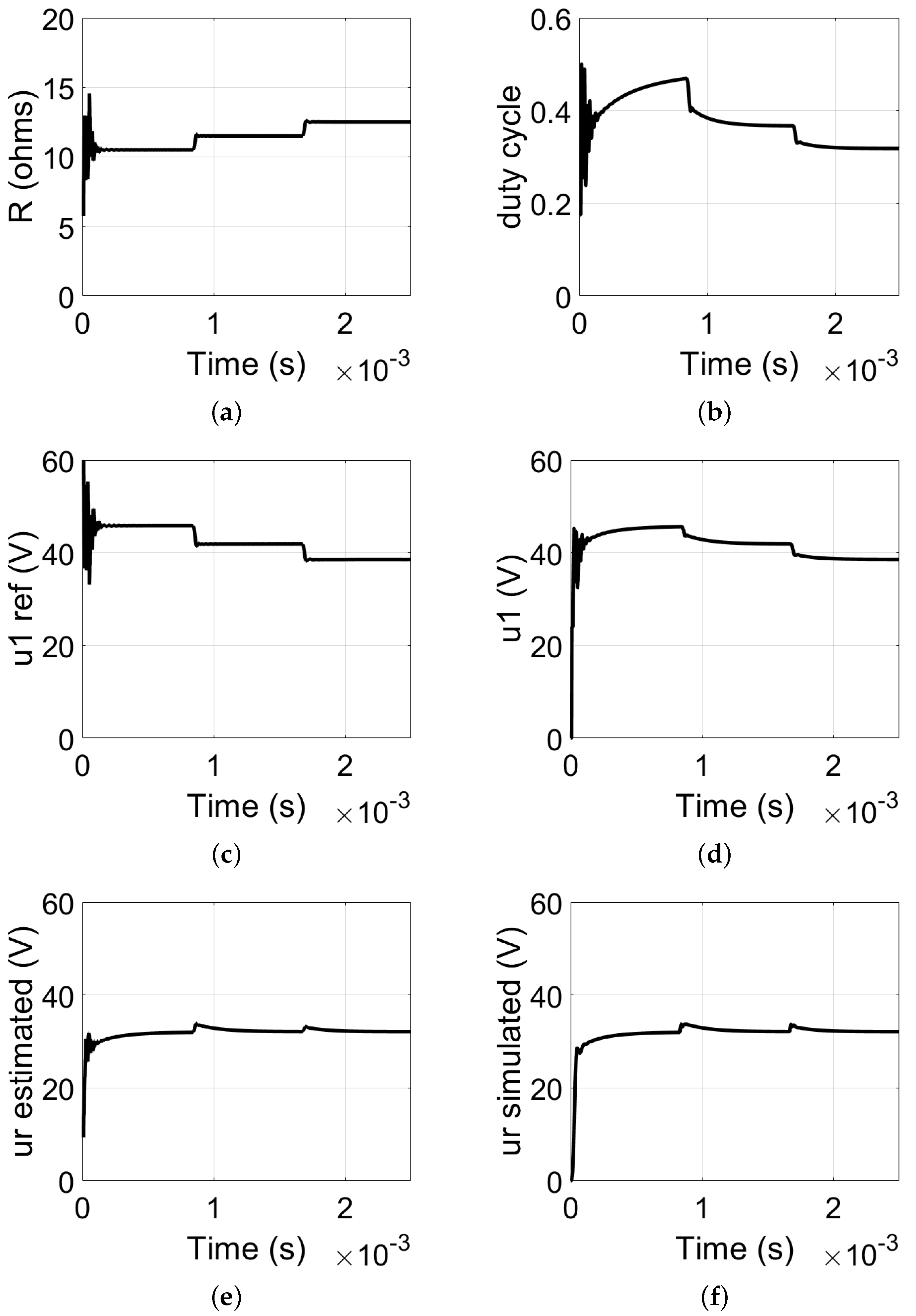
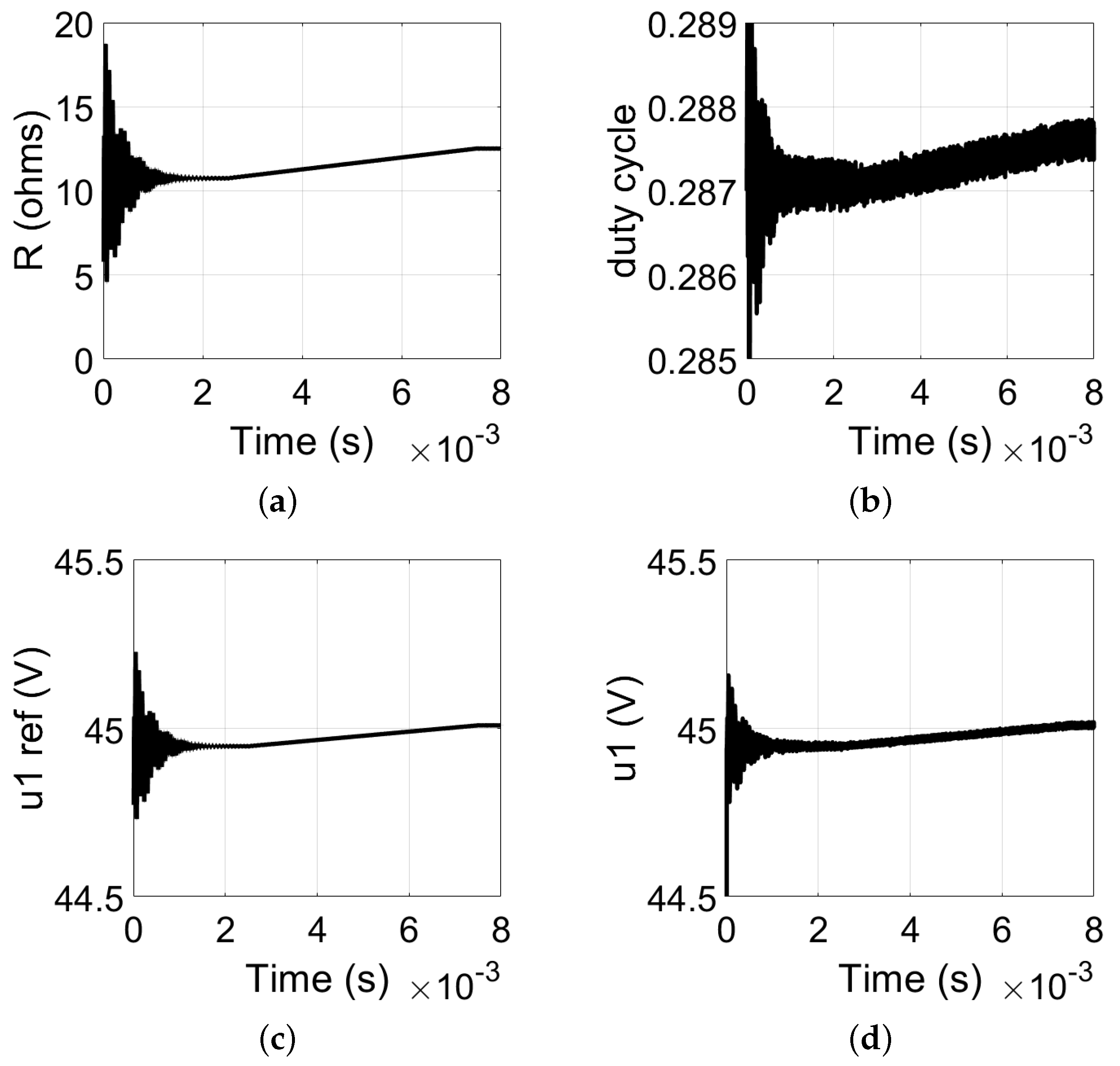
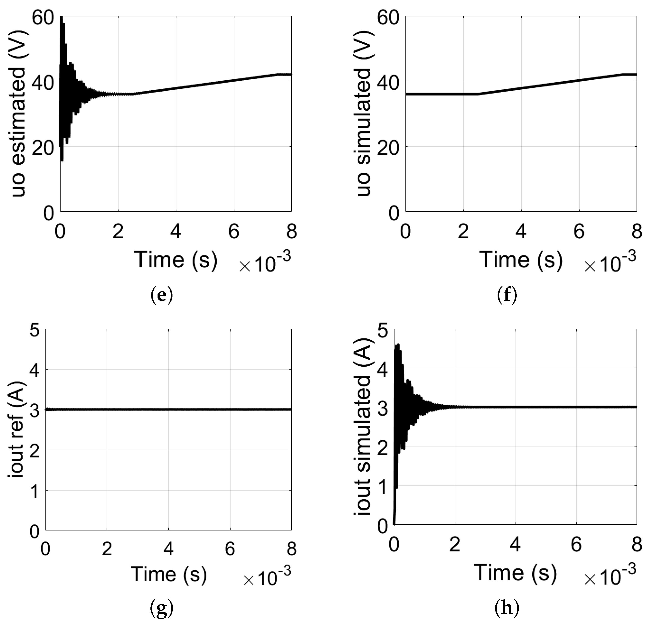
3.2. Current Source Operation
4. Conclusions
Author Contributions
Funding
Data Availability Statement
Acknowledgments
Conflicts of Interest
References
- Jiang, Y.; Wang, L.; Wang, Y.; Liu, J.; Wu, M.; Ning, G. Analysis, design, and implementation of WPT system for EV’s battery charging based on optimal operation frequency range. IEEE Trans. Power Electron. 2018, 34, 6890–6905. [Google Scholar] [CrossRef]
- Trivino, A.; González-González, J.M.; Aguado, J.A. Wireless power transfer technologies applied to electric vehicles: A review. Energies 2021, 14, 1547. [Google Scholar] [CrossRef]
- Agarwal, K.; Jegadeesan, R.; Guo, Y.X.; Thakor, N.V. Wireless Power Transfer Strategies for Implantable Bioelectronics. IEEE Rev. Biomed. Eng. 2017, 10, 136–161. [Google Scholar] [CrossRef] [PubMed]
- Pahlavan, S.; Jafarabadi-Ashtiani, S.; Mirbozorgi, S.A. Maze-Based Scalable Wireless Power Transmission Experimental Arena for Freely Moving Small Animals Applications. IEEE Trans. Biomed. Circuits Syst. 2025, 19, 120–129. [Google Scholar] [CrossRef] [PubMed]
- Pahlavan, S.; Shooshtari, M.; Jafarabadi Ashtiani, S. Star-Shaped Coils in the Transmitter Array for Receiver Rotation Tolerance in Free-Moving Wireless Power Transfer Applications. Energies 2022, 15, 8643. [Google Scholar] [CrossRef]
- Liu, F.; Yang, Y.; Jiang, D.; Ruan, X.; Chen, X. Modeling and Optimization of Magnetically Coupled Resonant Wireless Power Transfer System With Varying Spatial Scales. IEEE Trans. Power Electron. 2017, 32, 3240–3250. [Google Scholar] [CrossRef]
- Covic, G.A.; Boys, J.T. Inductive Power Transfer. Proc. IEEE 2013, 101, 1276–1289. [Google Scholar] [CrossRef]
- Wang, C.S.; Covic, G.; Stielau, O. Power transfer capability and bifurcation phenomena of loosely coupled inductive power transfer systems. IEEE Trans. Ind. Electron. 2004, 51, 148–157. [Google Scholar] [CrossRef]
- Carneiro, F.T.; Barbi, I. Análise, projeto e implementação de um conversor com transferência de energia sem fio para carregadores de baterias de veículos elétricos. Rev. Eletrônica -Potência-Sobraep 2021, 26, 260–267. [Google Scholar] [CrossRef]
- Ngini, M.A.; Truong, C.T.; Choi, S.J. Parameter Identification for Primary-Side Control of Inductive Wireless Power Transfer Systems: A Review. IEEE Access 2025, 13, 15885–15904. [Google Scholar] [CrossRef]
- Nath, S.; Lim, W.H.; Begam, K. Hybrid Inductive Power Transfer Topologies for Dynamic Wireless Power Transfer. Comput. Electr. Eng. 2024, 118, 109431. [Google Scholar] [CrossRef]
- Villa, J.L.; Sallan, J.; Osorio, J.F.S.; Llombart, A. High-misalignment tolerant compensation topology for ICPT systems. IEEE Trans. Ind. Electron. 2011, 59, 945–951. [Google Scholar] [CrossRef]
- Li, S.; Li, W.; Deng, J.; Nguyen, T.D.; Mi, C.C. A Double-Sided LCC Compensation Network and Its Tuning Method for Wireless Power Transfer. IEEE Trans. Veh. Technol. 2015, 64, 2261–2273. [Google Scholar] [CrossRef]
- Patil, D.; McDonough, M.K.; Miller, J.M.; Fahimi, B.; Balsara, P.T. Wireless Power Transfer for Vehicular Applications: Overview and Challenges. IEEE Trans. Transp. Electrif. 2018, 4, 3–37. [Google Scholar] [CrossRef]
- Jank, H.; Venturini, W.A.; Koch, G.G.; Martins, M.L.; Bisogno, F.E.; Montagner, V.F.; Pinheiro, H. Controle baseado em um LQR com estabilidade robusta a incerteza parametrica aplicado a um carregador de baterias. Rev. Eletrnica -Potencia-Sobraep 2017, 22, n4. [Google Scholar] [CrossRef]
- Vu, V.B.; Tran, D.H.; Choi, W. Implementation of the Constant Current and Constant Voltage Charge of Inductive Power Transfer Systems With the Double-Sided LCC Compensation Topology for Electric Vehicle Battery Charge Applications. IEEE Trans. Power Electron. 2018, 33, 7398–7410. [Google Scholar] [CrossRef]
- Meng, X.; Qiu, D.; Zhang, B.; Xiao, W. Output Voltage Stabilization Control without Secondary Side Measurement for Implantable Wireless Power Transfer System. In Proceedings of the 2018 IEEE PELS Workshop on Emerging Technologies: Wireless Power Transfer (Wow), Montreal, QC, Canada, 3–4 June 2018; pp. 1–5. [Google Scholar] [CrossRef]
- Meng, X.; Qiu, D.; Lin, M.; Tang, S.C.; Zhang, B. Output Voltage Identification Based on Transmitting Side Information for Implantable Wireless Power Transfer System. IEEE Access 2019, 7, 2938–2946. [Google Scholar] [CrossRef]
- Barbosa, C.R. Estudo de Sistemas de Transferência Indutiva de Potência Para Recarga de Baterias. Master’s Thesis, Escola de Engenharia de São Carlos, Universidade de São Paulo, São Carlos, Brazil, 15 May 2018. [Google Scholar] [CrossRef]
- Thrimawithana, D.J.; Madawala, U.K. A primary side controller for inductive power transfer systems. In Proceedings of the 2010 IEEE International Conference on Industrial Technology, Via del Mar, Chile, 14–17 March 2010; pp. 661–666. [Google Scholar] [CrossRef]
- Hoshikawa, H.; Koyama, K. Eddy current distribution using parameters normalized by standard penetration depth. In Review of Progress in Quantitative Nondestructive Evaluation; Springer: Berlin/Heidelberg, Germany, 1999; Volume 18A–18B, pp. 515–521. [Google Scholar]
- ABNT. NBR 5410: Low Voltage Electrical Installations, 2nd ed.; ABNT: Rio de Janeiro, Brazil, 2004; p. 209. (In Portuguese) [Google Scholar]
- Alexander, C.K.; Sadiku, M.N. Fundamentals of Electric Circuits; McGraw Hill: New York, NY, USA, 2021. [Google Scholar]
- Larbi, M.; Trinchero, R.; Canavero, F.G.; Besnier, P.; Swaminathan, M. Analysis of Parameter Variability in an Integrated Wireless Power Transfer System via Partial Least-Squares Regression. IEEE Trans. Compon. Packag. Manuf. Technol. 2020, 10, 1795–1802. [Google Scholar] [CrossRef]
- Li, D.; Wu, X.; Gao, J.; Lu, J.; Gao, W. Sensitivity Analysis and Parameter Optimization of Inductive Power Transfer. IEEE Access 2021, 9, 166951–166961. [Google Scholar] [CrossRef]
- Yang, J.; Zhang, X.; Zhang, K.; Cui, X.; Jiao, C.; Yang, X. Design of LCC-S Compensation Topology and Optimization of Misalignment Tolerance for Inductive Power Transfer. IEEE Access 2020, 8, 191309–191318. [Google Scholar] [CrossRef]
- Zhao, S.; Tang, C.; Fei, Y.; Deng, P. Research on order reduction and control of double-sided LCC wireless power transfer system based on GSSA model. In Proceedings of the 2022 IEEE 9th International Conference on Power Electronics Systems and Applications (PESA), Hong Kong, 20–22 September 2022; pp. 1–6. [Google Scholar]


| Variable | Primary Coil | Secondary Coil |
|---|---|---|
| 1.72 A | 1.72 A | |
| 0.07 m | 0.10 m | |
| Conductor | 6 × [AWG 26] | 6 × [AWG 26] |
| N | 110 | 54 |
| 16 cm | 8 cm | |
| 24 m | 17 m | |
| 360 μH | 360 μH | |
| 363.17 μH | 363.84 μH |
| Case | ||||||||||
|---|---|---|---|---|---|---|---|---|---|---|
| 1 | 90% | 107% | 102% | 110% | 101% | 99% | 112% | 89% | 100% | 118% |
| 2 | 101% | 107% | 105% | 102% | 95% | 107% | 83% | 105% | 106% | 115% |
| 3 | 108% | 110% | 105% | 102% | 109% | 103% | 81% | 85% | 115% | 110% |
| 4 | 107% | 94% | 101% | 103% | 91% | 105% | 94% | 82% | 100% | 104% |
| 5 | 92% | 94% | 93% | 94% | 91% | 105% | 91% | 102% | 108% | 110% |
| Parameter | Value |
|---|---|
| Transferred power (P) | 100 W |
| Switching frequency () | 120 kHz |
| Input voltage () | 36 V |
| Coupling factor (k) | 0.25 |
| Transmitter coil inductance () | 360 μH |
| Receiver coil inductance () | 360 μH |
| Filter inductance () | 35.41 μH |
| Filter inductance () | 35.41 μH |
| Filter capacitance () | 49.67 nF |
| Filter capacitance () | 49.67 nF |
| Primary capacitance () | 5.42 nF |
| Secondary capacitance () | 5.42 nF |
| Transmitter coil resistance () | 541.50 m |
| Receiver coil resistance () | 541.50 m |
| Filter inductance resistance () | 3.10 m |
| Filter inductance resistance () | 3.10 m |
Disclaimer/Publisher’s Note: The statements, opinions and data contained in all publications are solely those of the individual author(s) and contributor(s) and not of MDPI and/or the editor(s). MDPI and/or the editor(s) disclaim responsibility for any injury to people or property resulting from any ideas, methods, instructions or products referred to in the content. |
© 2025 by the authors. Licensee MDPI, Basel, Switzerland. This article is an open access article distributed under the terms and conditions of the Creative Commons Attribution (CC BY) license (https://creativecommons.org/licenses/by/4.0/).
Share and Cite
Tolfo, T.M.; Silva, R.d.S.; Godoy, R.B.; de Brito, M.A.G.; de Souza, W.S. Parameter Estimation-Based Output Voltage or Current Regulation for Double-LCC Hybrid Topology in Wireless Power Transfer Systems. Energies 2025, 18, 2664. https://doi.org/10.3390/en18102664
Tolfo TM, Silva RdS, Godoy RB, de Brito MAG, de Souza WS. Parameter Estimation-Based Output Voltage or Current Regulation for Double-LCC Hybrid Topology in Wireless Power Transfer Systems. Energies. 2025; 18(10):2664. https://doi.org/10.3390/en18102664
Chicago/Turabian StyleTolfo, Thaís M., Rafael de S. Silva, Ruben B. Godoy, Moacyr A. G. de Brito, and Witória S. de Souza. 2025. "Parameter Estimation-Based Output Voltage or Current Regulation for Double-LCC Hybrid Topology in Wireless Power Transfer Systems" Energies 18, no. 10: 2664. https://doi.org/10.3390/en18102664
APA StyleTolfo, T. M., Silva, R. d. S., Godoy, R. B., de Brito, M. A. G., & de Souza, W. S. (2025). Parameter Estimation-Based Output Voltage or Current Regulation for Double-LCC Hybrid Topology in Wireless Power Transfer Systems. Energies, 18(10), 2664. https://doi.org/10.3390/en18102664