1. Introduction
The widespread deployment of DC microgrids in industrial and commercial applications has intensified the demand for high-power-density multiport converters that are capable of efficient multi-directional power flow management [
1,
2,
3,
4,
5]. Typically, isolated DC/DC converters for distributed energy resources (DERs) and bidirectional non-isolated buck/boost converters for battery integration are designed separately for the convenience of simple control and easy implementation. However, decoupling DER interfaces and storage converters substantially increases the component count compared to integrated multiport solutions [
6], escalating system cost and coordination difficulties. The main limitation of this is the significant efficiency degradation, especially in relation to the cascaded LLC resonant converters with auxiliary circuits that are widely used for wide voltage gain ranges under partial-load conditions. Therefore, exploring the methods with which to develop the single-stage multiport DC/DC converters to consolidate renewable energy integration, storage management, and load regulation into a unified converter in order to achieve high efficiency and a wide adjustment range is a key goal for the development of DC microgrids.
Table 1 presents a performance comparison of isolated and non-isolated three-port converters in relation to different aspects. Non-isolated designs achieve marginally higher peak efficiency (97–99%) by eliminating transformer losses, but their reliance on cascaded stages introduces 5–8% system-level efficiency penalties and high inter-port coupling (10–15%). In contrast, isolated converters inherently provide galvanic isolation and natural port decoupling (<5% coupling), enabling wide voltage ratio adaptation through the optimization of the transformer turns ratio. While non-isolated architectures initially excel in cost (20% lower magnetic costs) and power density (300–500 W/in
3), emerging magnetic integration techniques and hybrid modulation strategies [
7] have narrowed these gaps, achieving a density of 300 W/in
3 and a partial-load efficiency of 94% in isolated designs. Crucially, isolated topologies align with future DC microgrids that demand multi-energy integration and high-voltage scalability, justifying their dominance in safety-critical applications.
Recent innovations in isolated multiport converters address cost-efficiency challenges through strategic topology synthesis [
12]. The proposed three-port LLC resonant DC/DC converter adopts an innovative architecture that combines an asymmetric fixed-frequency full-bridge LLC network with a cascaded H-bridge structure, which significantly improves the conversion efficiency by reducing energy conversion links, simplifying component design, and efficiently managing power flow [
13]. A structural reconfigurable LLC (SR-LLC) resonant converter was proposed to implement four operating modes through the dual-resonant tank-sharing bridge arm, which expands the voltage gain range, achieves soft switching and optimized parameter design, and improves efficiency. However, conventional LLC circuits face voltage gain limitations, necessitating auxiliary strategies like switched-capacitor arrays [
14] or dual-transformer configurations [
15] in order to meet wide voltage ratio requirements. These solutions incur significant cost penalties, highlighting the need for resonant parameter adaptability without compromising device-sharing benefits.
To overcome voltage gain constraints and efficiency deduction, advanced control strategies have emerged. A unified PWM-PFM phase shift control and closed-loop control strategy for bidirectional DC/DC converters with a dual active bridge [
16] is proposed to avoid DC current bias, accelerate phase shift, and reduce AC transient influence. With this closed-loop control strategy, the converters can achieve stable switching within 1 ms, which effectively improves the stability and reliability of the system [
17]. The bidirectional hybrid DC/DC resonant converter adopts a multi-mode switching control and a smooth mode switching strategy based on frequency matching, which makes the peak efficiency of the forward operation reach 97.3% and the peak efficiency of the reverse operation reach 96.5%. The authors of [
18] proposed a multi-output DC/DC topology based on pulse frequency modulation (PFM) and phase-shift hybrid modulation. The hybrid modulation strategy was adopted to achieve independent multi-output control without cross adjustment, reduce the resonant current, improve system efficiency, and achieve zero-voltage power switching [
19]. However, it is still challenging when optimizing the power flow balance and high efficiency of the LLC converters, which are demanded simultaneously [
20,
21,
22].
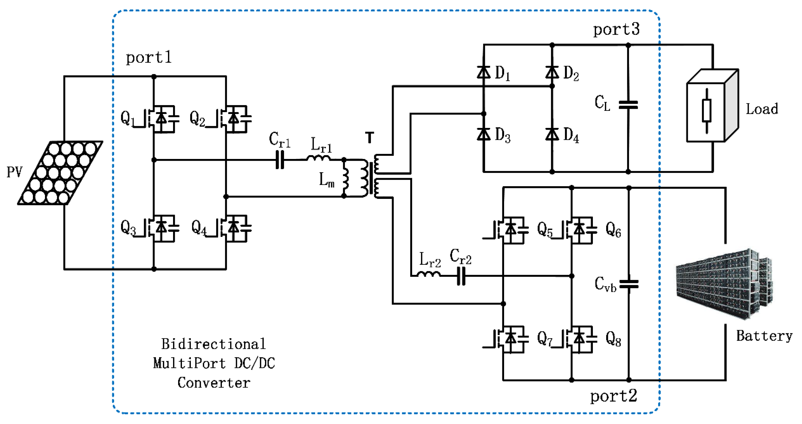
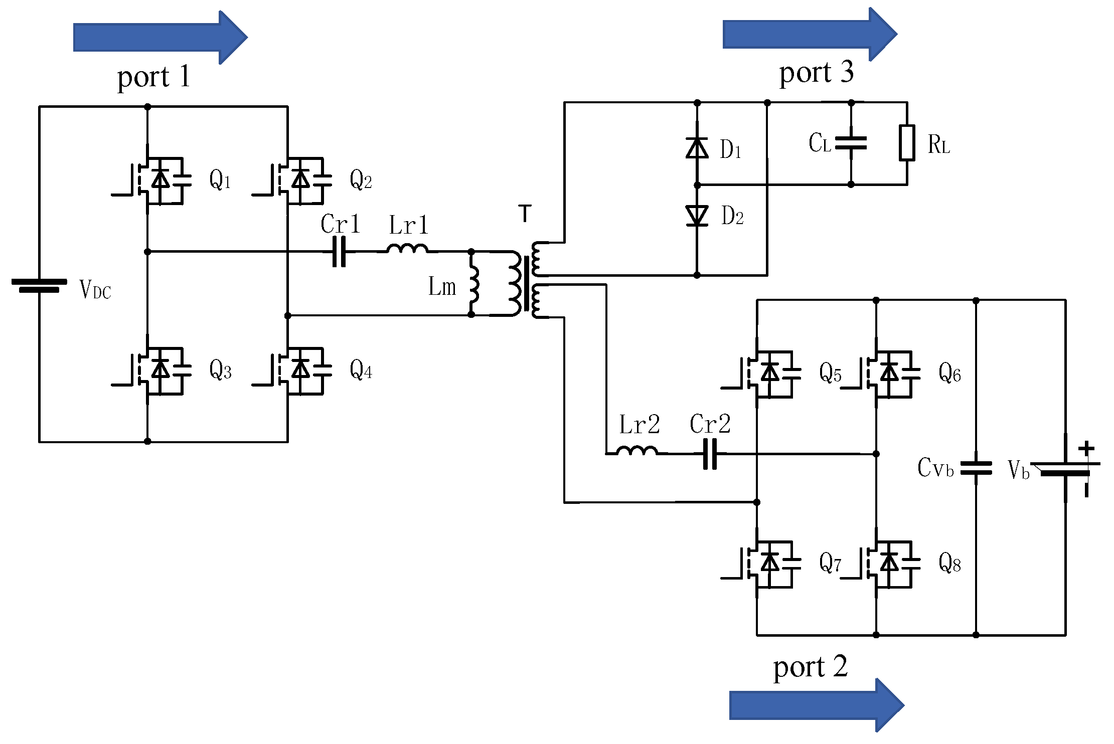
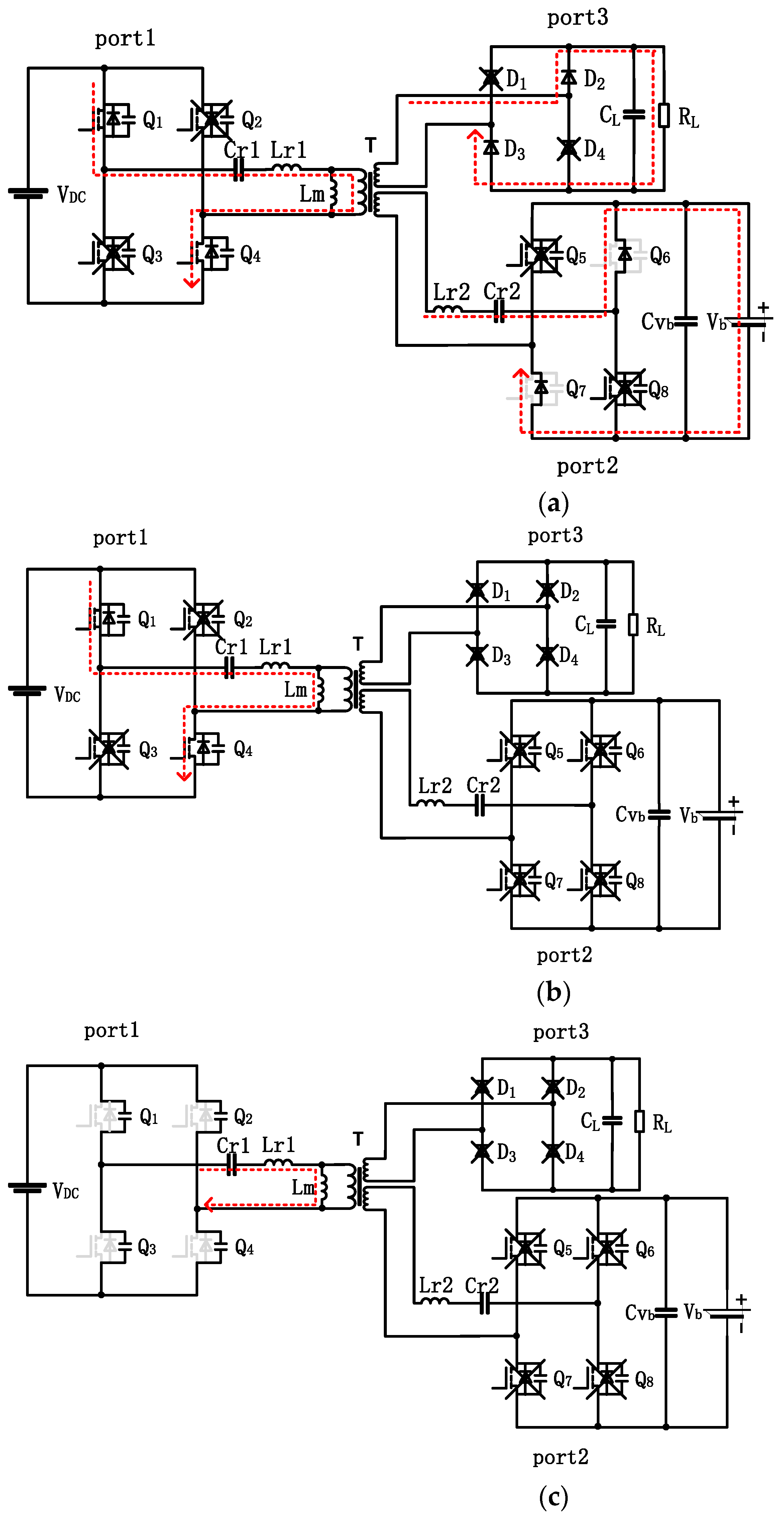
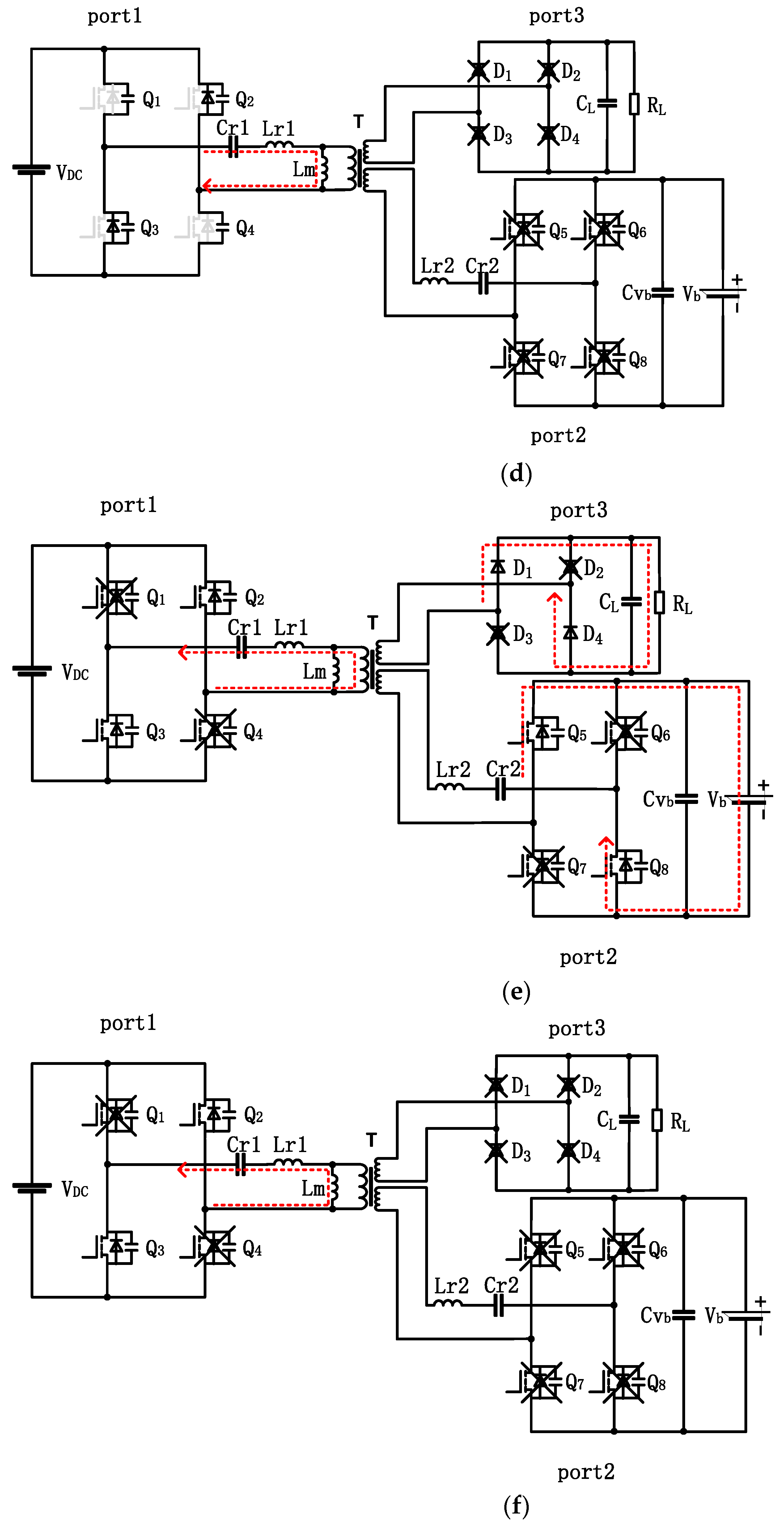
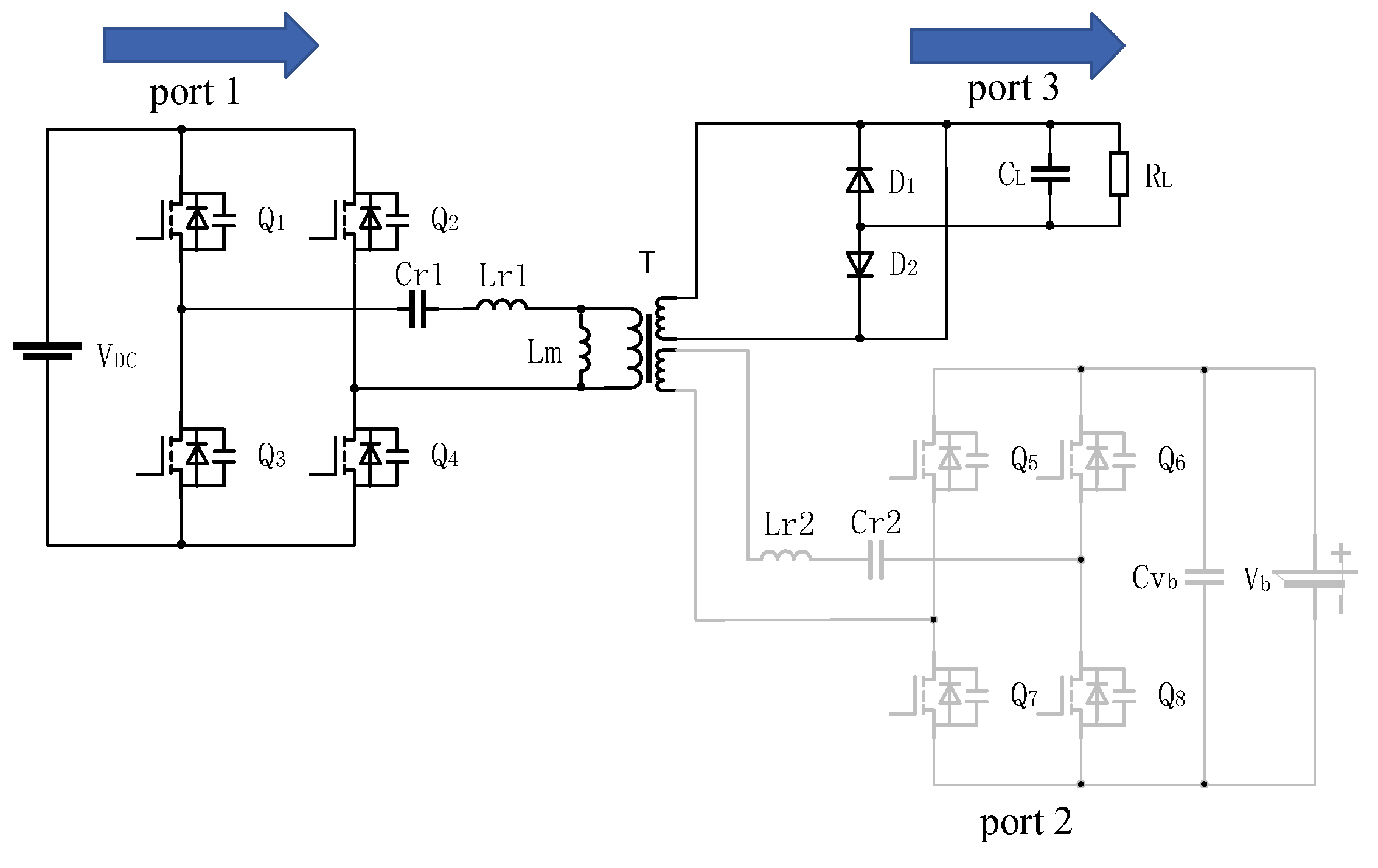
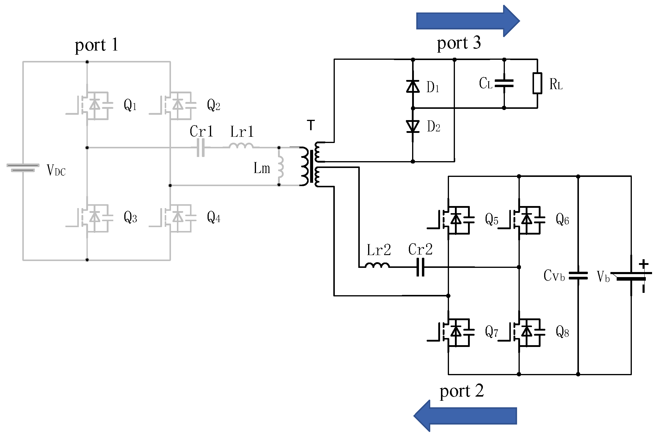
This article presents a novel isolated three-port converter that is tailored for DC microgrids, addressing efficiency, scalability, and control challenges in relation to multi-energy integration. Specifically, the proposed topology enables seamless power flow management across high-voltage DC buses, energy storage systems, and PV under various conditions. Therefore, the main contributions of the converter include the following.
- (1)
Single-stage High-efficiency Power Conversion: The integration of a dual active bridge (DAB)–LLC resonant structure with interleaved buck/boost stages eliminates cascaded conversion losses. Energy flows bidirectionally between ports (e.g., 150–300 V storage to ±48 V DC bus) via zero-voltage switching (ZVS), achieving 97.2% efficiency across 150–300 V input ranges, which is a 15% improvement over conventional cascaded designs.
- (2)
Multiport Power Sharing: A hybrid PWM-PFM phase shift control scheme dynamically allocates power between ports without altering switching frequency. By decoupling power regulation (coupling < 5%) and leveraging resonant tank optimization, this strategy reduces control complexity while maintaining a ±2.5% voltage ripple under 20% load transients.
- (3)
Wide Voltage Ratio Adaptability: A switch-controlled capacitor network and frequency tuning enable resonant parameter adjustment, achieving a 1:2 voltage gain range without auxiliary circuits. It reduces cost penalties compared to dual-transformer solutions, making the topology viable for heterogeneous DC microgrids.
3. Quantified Analysis
3.1. Voltage Gain Analysis
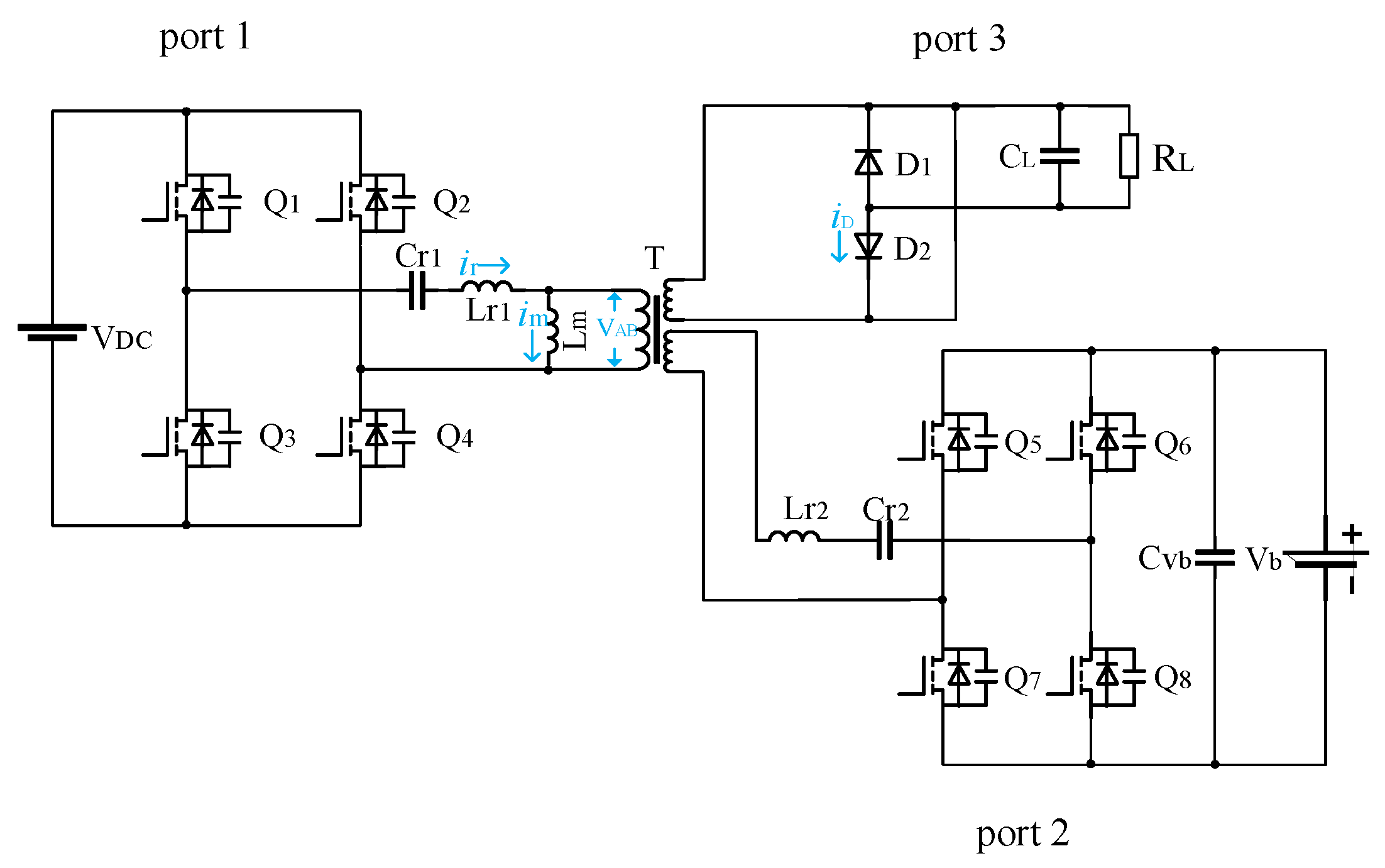
To more clearly illustrate the operation principle, this section analyzes the voltage regulation capability and ZVS by utilizing the equations for the voltage gain of the LLC portion.
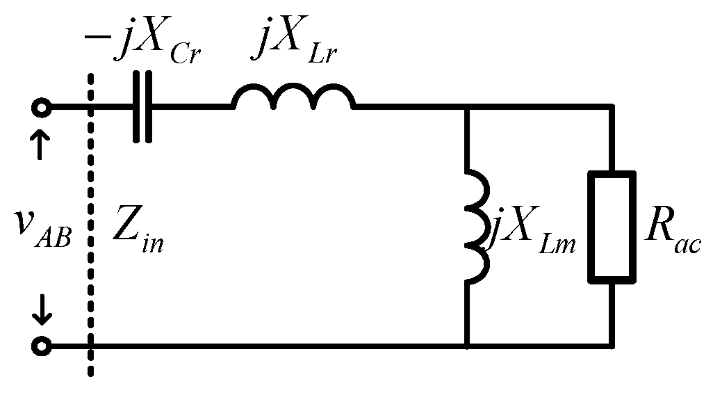
Figure 8 depicts a three-port LLC resonant converter First Harmonic Approximation (FHA) equivalent AC circuit [
23].
XCr =
ωsL
Cr,
XLr =
ωsL
r, and
XLm =
ωsL
m are the complex impedance of the resonant capacitor, resonant inductance, and magnetizing inductance, respectively.
Zin is the equivalent input impedance of the circuit.
The voltage,
VT2, on the secondary side of the transformer is a square wave signal, which can be expressed as a Fourier expansion, as follows:
Taking the effective value of its fundamental component, the following is obtained:
The secondary current,
IT2, is approximately equivalent to a sine wave; then, the relationship between
Io and
IT2 is determined as follows:
It can be concluded that the equivalent AC load is as follows:
whereas the input impedance of the converter can be obtained from the following analysis:
where
is the switching angular frequency.
Assume the switching angular frequency is
and define
. Then, the impedance angle
of the circuit can be obtained from Equation (5), as follows:
Thus, the related AC voltage gain for the proposed scheme is derived as follows:
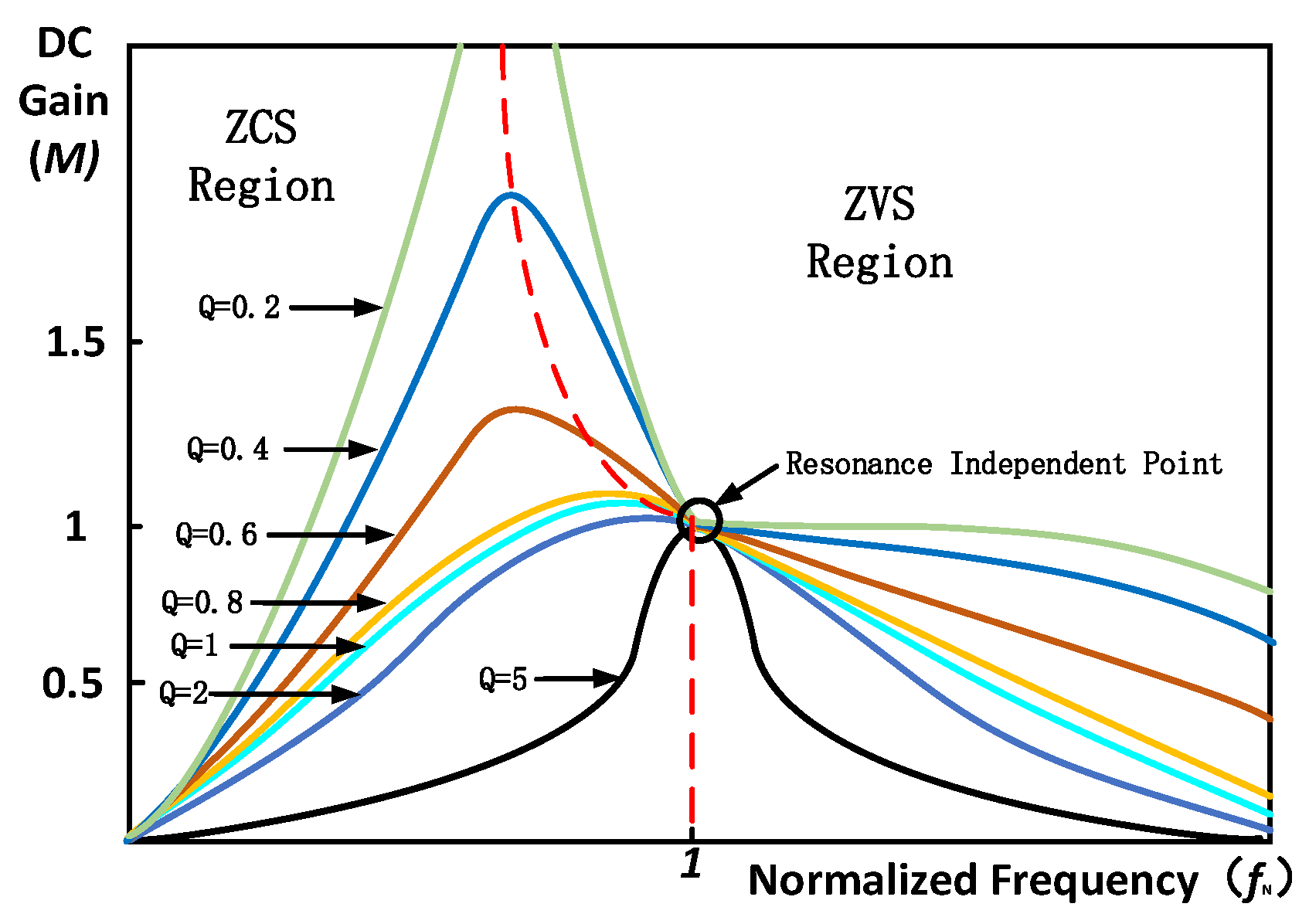
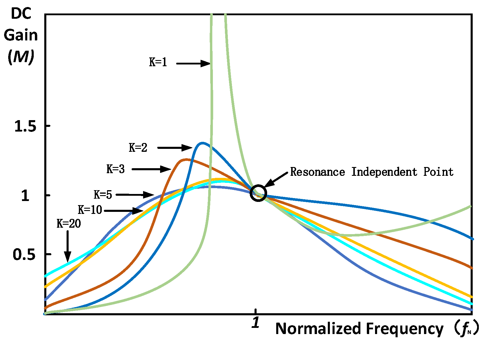
Redefine the following variables: is the ratio of magnetizing inductance to resonance inductance; is the normalized frequency; and is the quality factor.
Then, by simplifying Equation (7), taking the modulus of the frequency response function after simplification, the DC voltage gain of the proposed converter from the PV port to the output port can be obtained, as follows:
Based on the abovementioned analysis,
Figure 9 and
Figure 10 show the relationships between
,
, and gain
. It can be seen from
Figure 9 that, when the normalization frequency is less than 1, m increases with increases in
, whereby, when the
value is large, it increases first, but decreases when the
value is small. When the normalization frequency is greater than 1, no matter how large the
value is,
decreases with increases in
. From Equation (8), it is easy to see that, when
,
is always equal to 1, regardless of the change in quality factor and inductance proportional coefficient.
When the quality factor is fixed, regardless of the value of
,
always increases first, and then decreases with the increase in normalized frequency, as shown in
Figure 10. Similarly, each gain curve passes through the resonant independent point. From the curve characteristics, it can be seen that, the larger the
value, the more stable the characteristic curve is, which is conducive to the stability of the converter.
3.2. Parameter Analysis of Three-Port LLC Resonant Converters
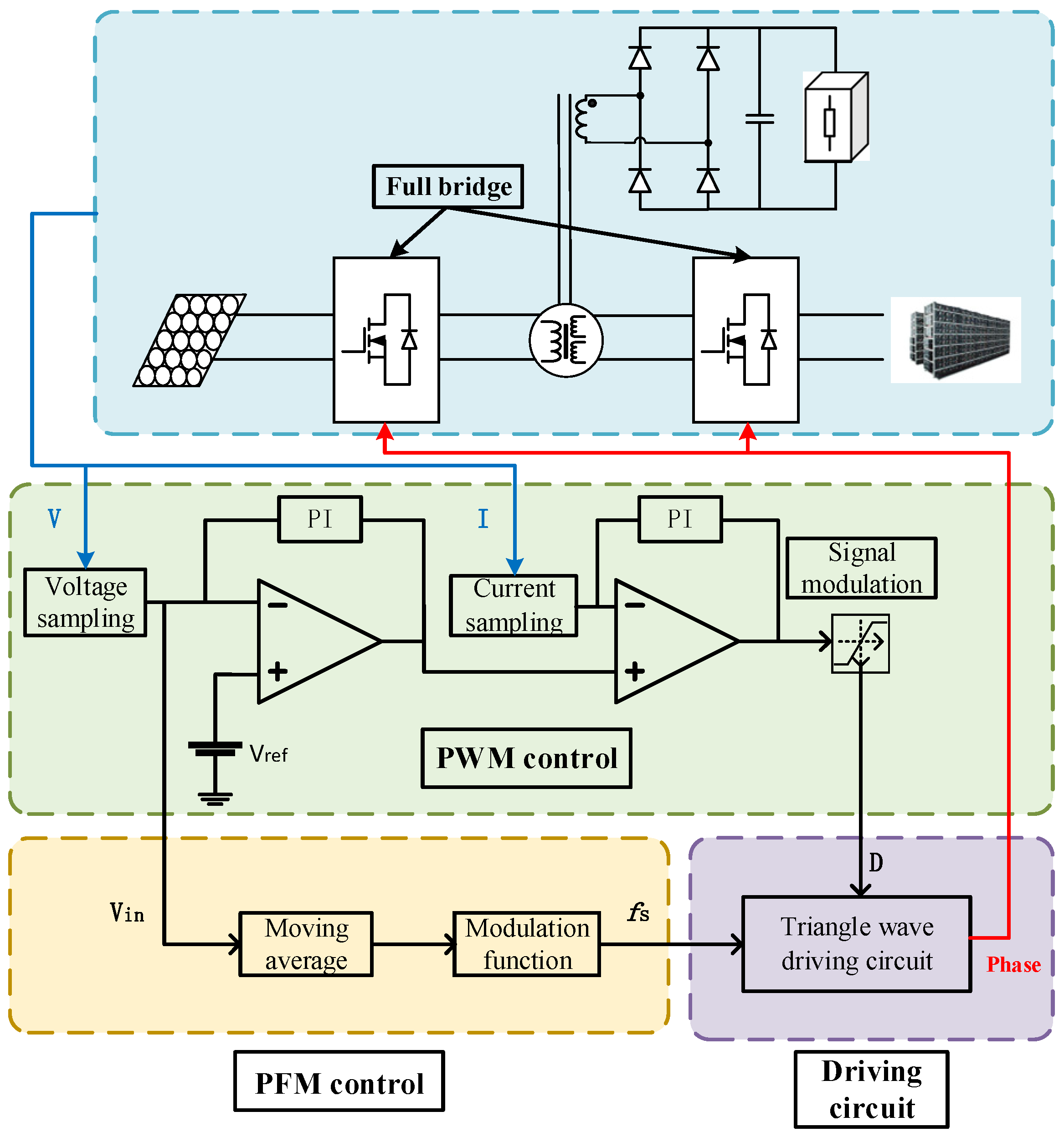
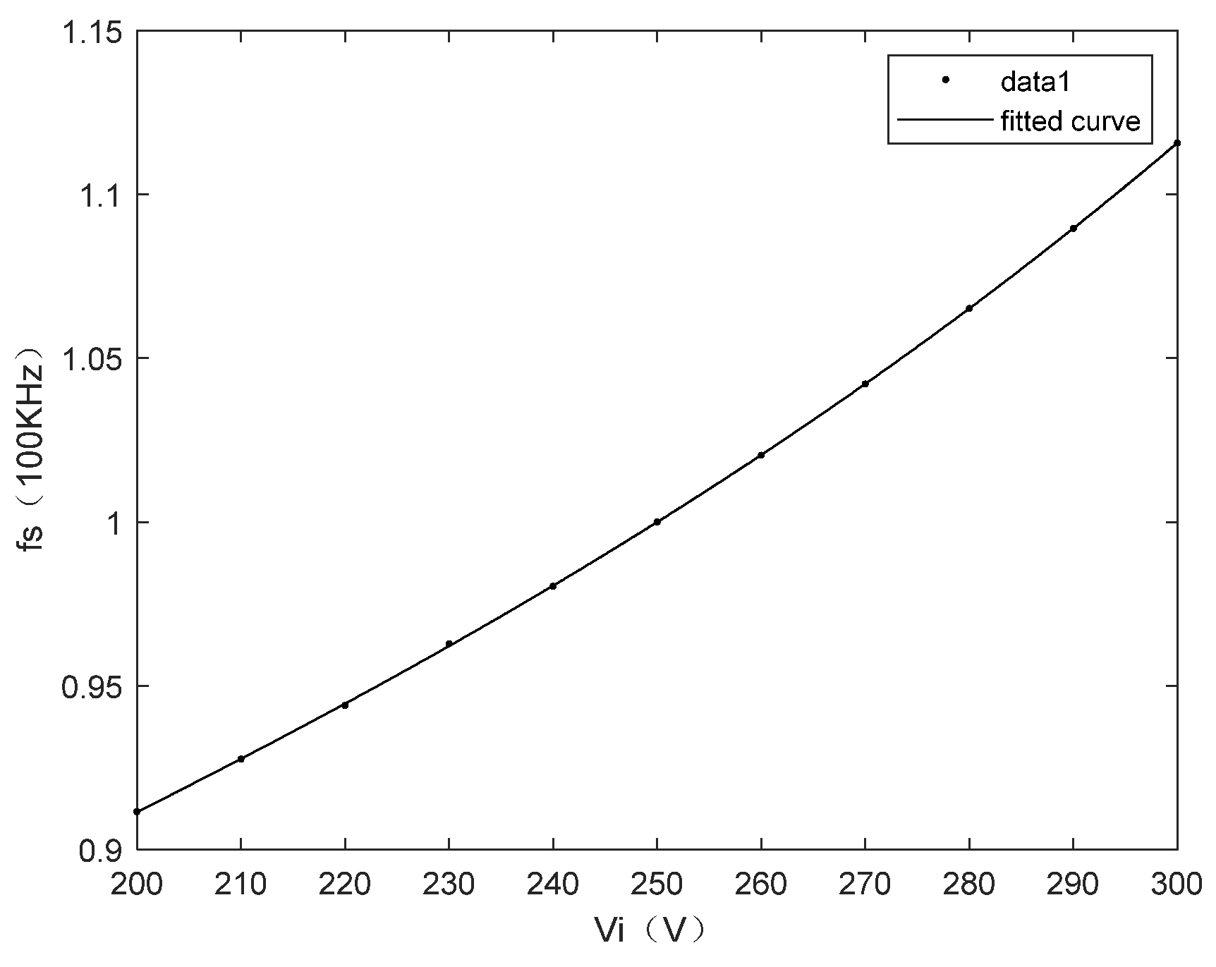
According to the design target of the three-port converter, the following mathematical model is established to calculate the converter parameters. The following parameters are selected: input voltage Vin = 150~300 V; output voltage Vo = 48 V; output power Po = 480 W; and switching frequency fs = 91.16~111.57 KHz.
From the principle of the LLC resonant converter, when the ratio
K of the magnetizing inductance to the resonant inductance is determined, the increase in the quality factor
Q will cause the voltage gain to decrease. In order to keep the output voltage constant, the converter will reduce the switching frequency to obtain a greater voltage gain. When the converter works under heavy load conditions, reducing the working frequency will make the converter work in a capacitive state, and the soft switching technology cannot be utilized. Therefore, a reasonable design of the quality factor is very important to the soft-switching characteristics of the converter.
The requirement for the converter to work in an inductive state is that the quality factor is lower than Qmax. Generally, in this design, is taken as the quality factor of the converter, while Q = 0.38.
- 2.
Transformer turns ration
From Equation (8), the transformer turn ratio n satisfies the following relationship:
According to the design target, the minimum input voltage Vin = 200 V. K = 4 is the ratio of magnetizing inductance to resonance inductance. In order to make the change range of the switching frequency as small as possible, the following parameters are chosen: fs_min = 0.91 kHz; normalized frequency fs_min = 0.93; and Qmax = 0.38. Through calculation, n = 5.4.
- 3.
The resonance parameters Lr, Cr, and Lm are calculated as follows:
The resonant inductance and the resonant capacitor values are Lr = 119.77 µH; Cr = 21.15 nF; and Lm = 479.06 µH.
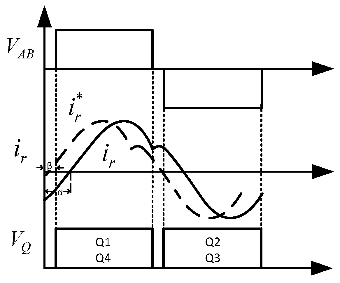
3.3. Calculation for ZVS Conditions
The ZVS of the converter can be achieved if there is no forward voltage at the moment when the switch tube is turned on. Assuming that all components are in an ideal state, the key waveform of the port 1 switch is shown in
Figure 11.
is the resonant current in the ideal state, while
is the actual resonant current, as shown in
Figure 11.
β is the conduction delay angle of the switching tube. The magnitude of
β is determined by the dead time of the switching tube, and its value can be obtained through Equation (14).
α is the impedance angle of the circuit, and its value can be calculated by Equation (5). According to
Figure 11, the conditions needed to achieve ZVS are as follows:
According to
Figure 11 and Equation (15), it can be concluded that the ZVS of the switch tube needs to have a sufficiently large impedance angle. The input impedance of the converter is related to parameters such as resonant inductance/capacitance, magnetizing inductance, and equivalent AC load. Therefore, the soft switching technology of the switch tube can be determined by rationally designing the parameters of the converter.
5. Simulation and Experimental Results
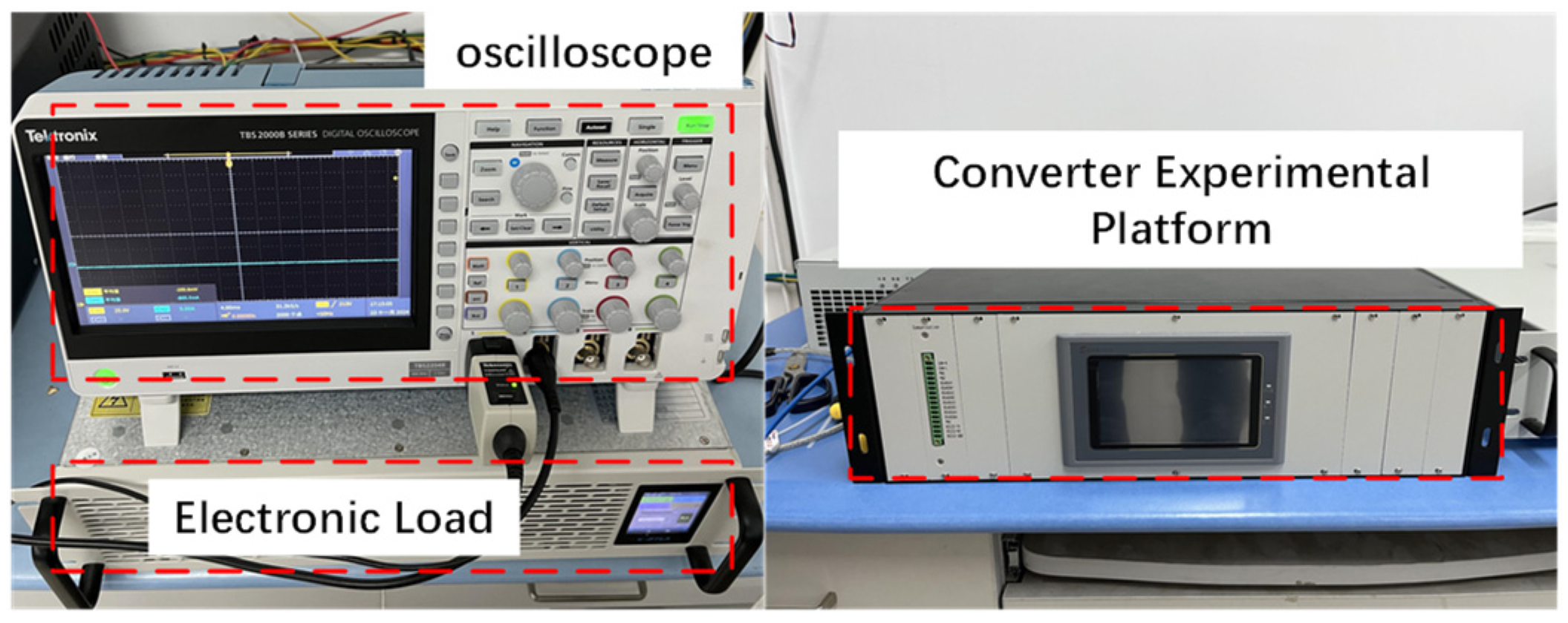
To verify the principle and soft-switching feature of the proposed topology, a prototype is built by using the following specifications.
- (1)
Input voltage: 200–300 V;
- (2)
Output voltage of the secondary side: 380 V;
- (3)
Battery voltage: 48 V;
- (4)
Maximum output current: 5 A;
- (5)
Switching frequency: 88.43~116.44 kHz.
A picture of the prototype is shown in
Figure 14, while
Table 3 shows the parameter comparison. In the test platform, the resonant inductor adopts an EE20/20/5 magnetic core. The model of the resonant capacitor is BFC233820223, and the AC working voltage of this model can reach 310 v. The model of the primary side power tube is STD11NM65N, the model of the secondary side power tube is SCTH40N120G2V7AG, and each synchronous rectifier tube (d1–d2) is Si4435DY (30 V, 10 m Ω, SO-8 package).
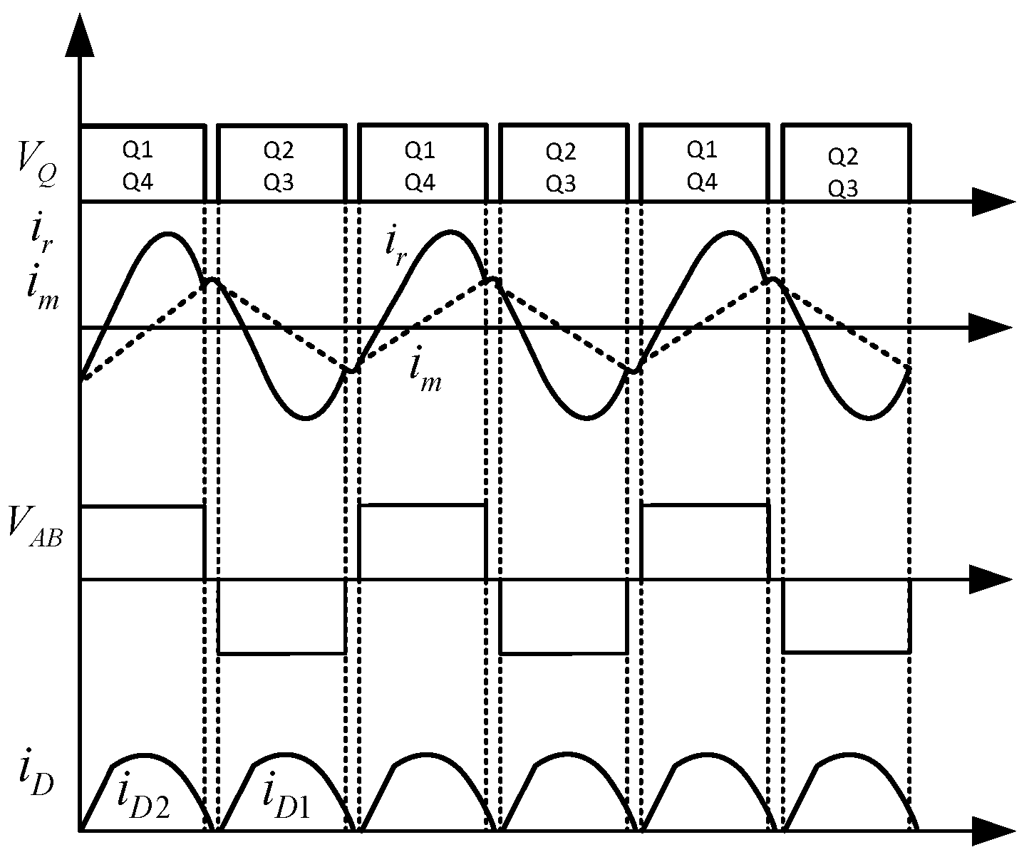
5.1. ZVS Analysis of Three-Port LLC Resonant Converters
This section mainly compares the ZVS characteristics of conventional PWM-PFM [
24,
25] and improved PWM-PFM control. According to the theoretical analysis in
Section 3.2, the ZVS of the switch tube can be achieved if the circuit impedance angle is greater than the switch conduction delay angle β. Observing the
Q1 and
Q2 states can determine whether the converter is in the ZVS state, because of the symmetry of the full-bridge structure.
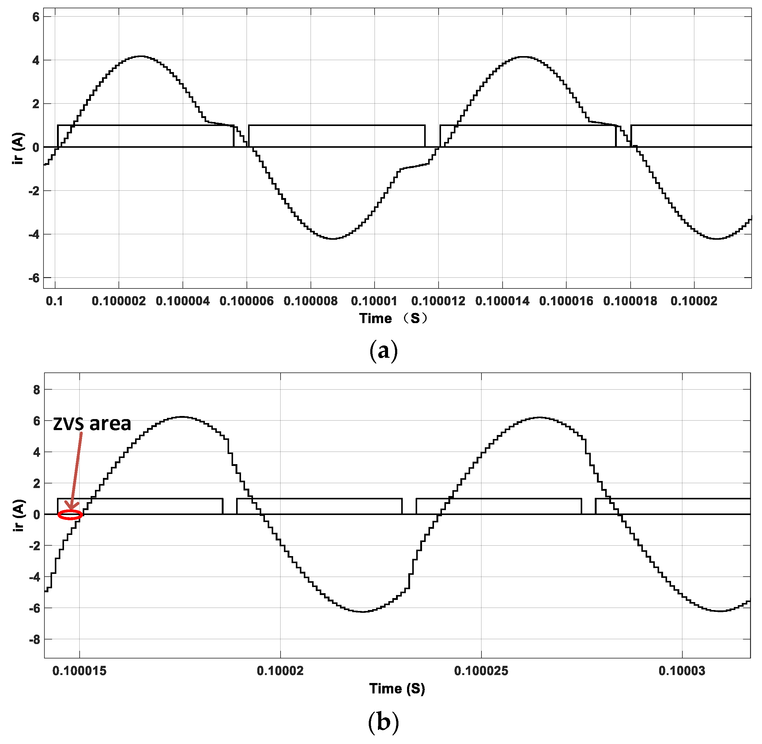
Figure 15 illustrates the relationship between the switch trigger signal and its corresponding current waveform under conventional PWM-PFM control.
According to the characteristics of LLC resonant converters, when the converter works under a high input voltage, it is difficult to determine the ZVS of the switch tube; on the contrary, it is easier to determine the ZVS under a low input voltage. It can be seen from
Figure 11 that the converter cannot achieve ZVS when
Vin = 150 V. As the input voltage increases, the ZVS characteristic of the converter becomes better. The converter has a large ZVS margin when the input voltage is at 300 V.
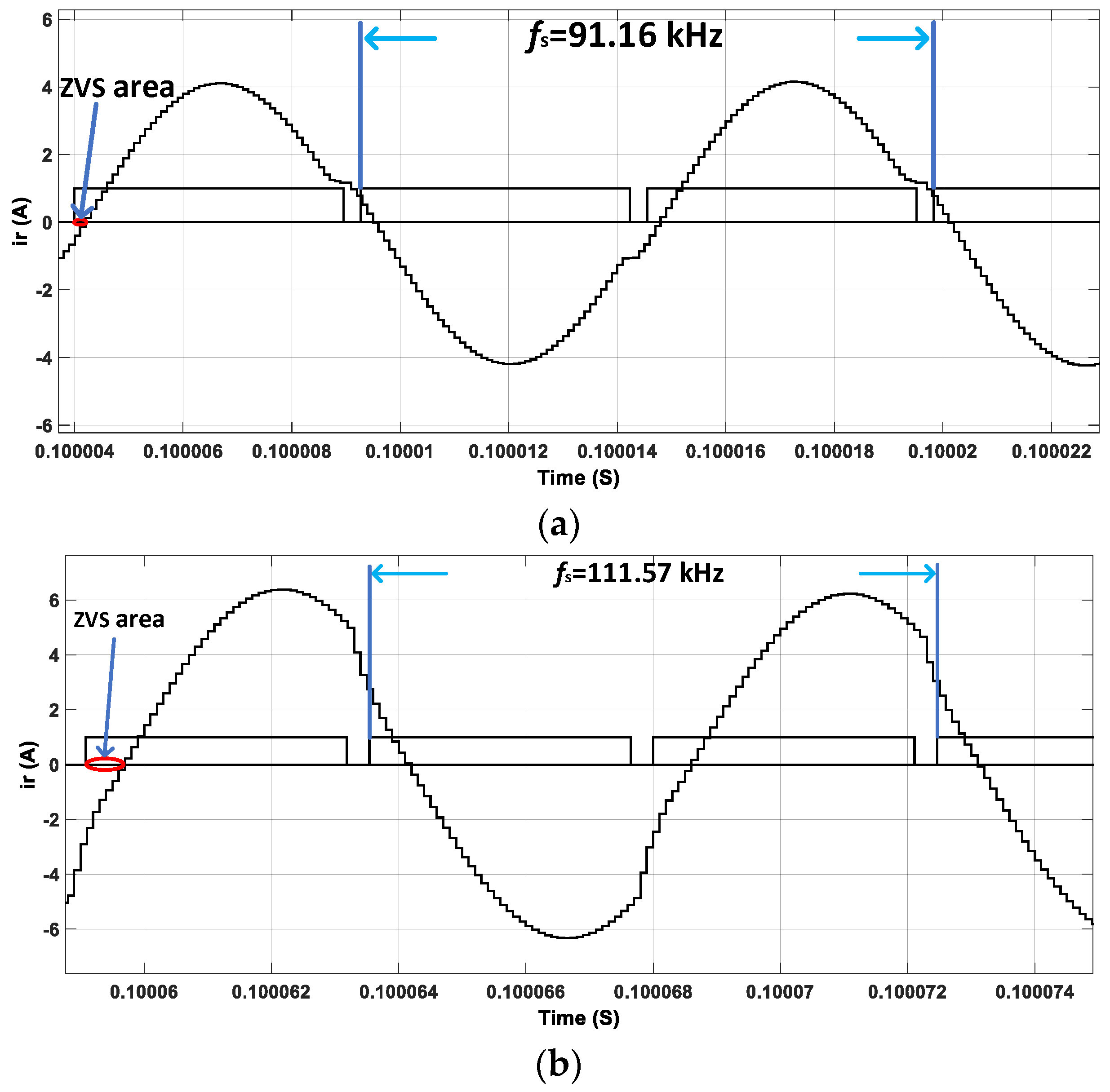
The ZVS waveform under the improved PWM-PFM control strategy proposed in this article is shown in
Figure 16. From the simulation results, the three-port LLC resonant converter can achieve ZVS in a wide input voltage range under the PWM-PFM hybrid control strategy. The resonant frequency of the converter is 91.16 kHz at a 150 V input voltage. Under this working condition, the switch tube can determine the ZVS, but the ZVS area is narrow. When the converter is at a high input voltage of 400 V, the resonance frequency is 116.44 kHz, and the converter has a larger ZVS margin at this time.
Under heavy-load conditions, the fundamental value of the input voltage and the phase of the resonant current are the same, the circulating current in the resonant tank is lower, and the ZVS characteristic is improved. Conversely, as the converter enters the light-load mode, because the phase difference between them increases, the circulating current becomes larger and the ZVS characteristic becomes worse. Based on this phenomenon, upon changing the working frequency of the converter, the converter still has a wider ZVS area under high input voltage conditions.
5.2. Analysis of Output Characteristics of Three-Port LLC Resonant Converters
This section compares the output characteristics of conventional PWM-PFM and improved PWM-PFM control.
Figure 13 depicts the output waveform under PWM control.
The output waveform of the converter under
Vin = 150 V is shown in
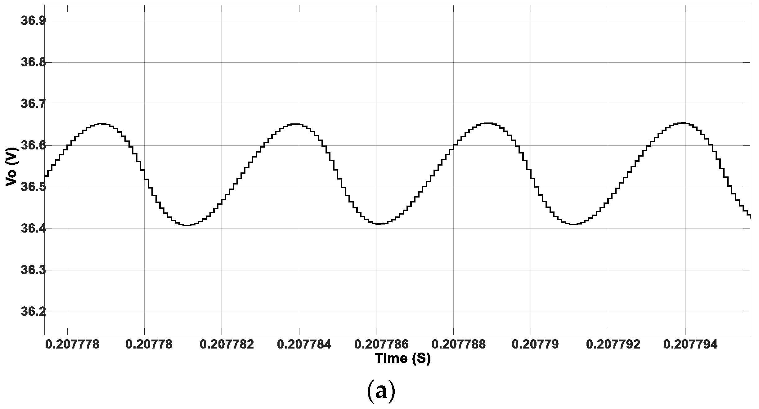
Figure 17a. At
Vin =150 V, the output voltage is around 36.5 V under conventional PWM-PFM modulation. Obviously, the converter cannot stabilize the output voltage at 48 V. From this state, as
Vin increases,
Vo begins to increase. As shown in
Figure 17b, when the input voltage reaches V
in_max = 300 V, the output voltage
Vo = 54.6 V, which also cannot be stabilized at 48 V. Therefore, the converter cannot achieve output voltage stabilization at a wide input voltage.
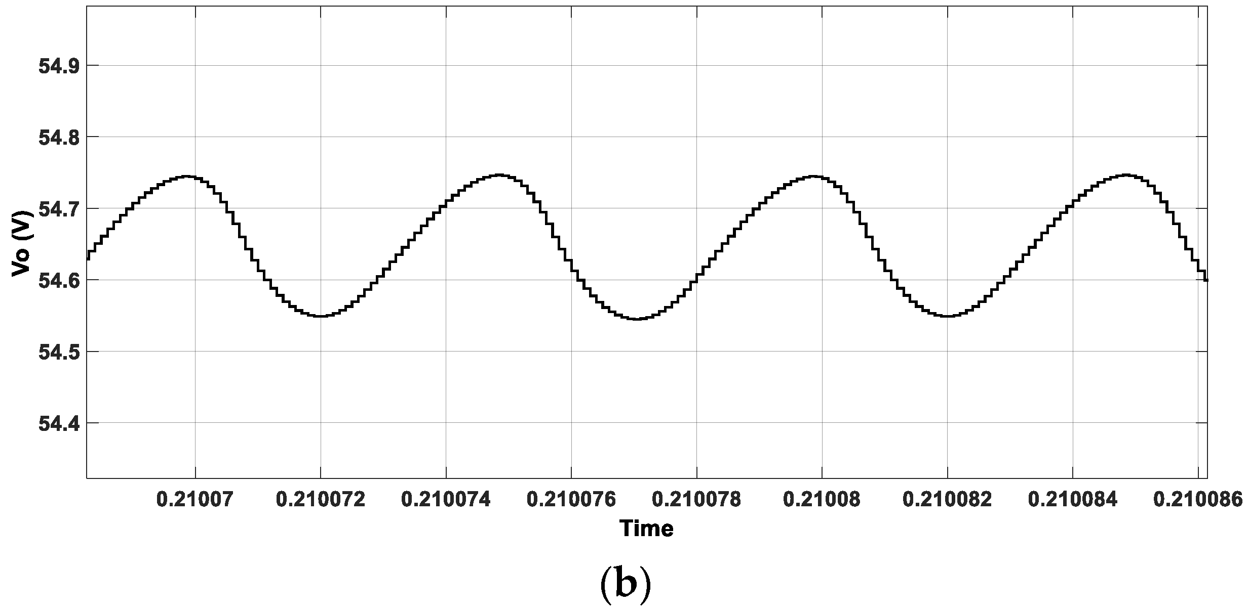
The output waveform under the improved PWM-PFM hybrid control strategy proposed in this article is shown in
Figure 18. As shown in
Figure 18a,
Vin = 150 V, and frequency
fs = 91.16 kHz. The error of the converter output voltage accounts for 0.0792% of the rated value. It can be inferred that, when the input voltage
Vin =
Vin_min, the converter can complete the modulation of the output voltage. Similarly, as shown in
Figure 18b,
Vin = 300 V, and frequency fs = 111.57 kHz. In this state, the error of the converter accounts for 0.0917%, which is slightly larger than that under low input voltage.
The improved PWM-PFM system has a greater advantage compared to the system only consisting of PWM. In the PWM-PFM hybrid system, the converter has voltage stabilization characteristics and ZVS characteristics under a wide input voltage. In this design, the input voltage changes from 150 V to 300 V, the converter can always be in the ZVS state, and the output voltage can be stabilized. The three-port structure reduces the number of components and ZVS in a wide range, reducing the energy loss.
5.3. PWM-PFM Experimental Verification
5.3.1. The Load Increases
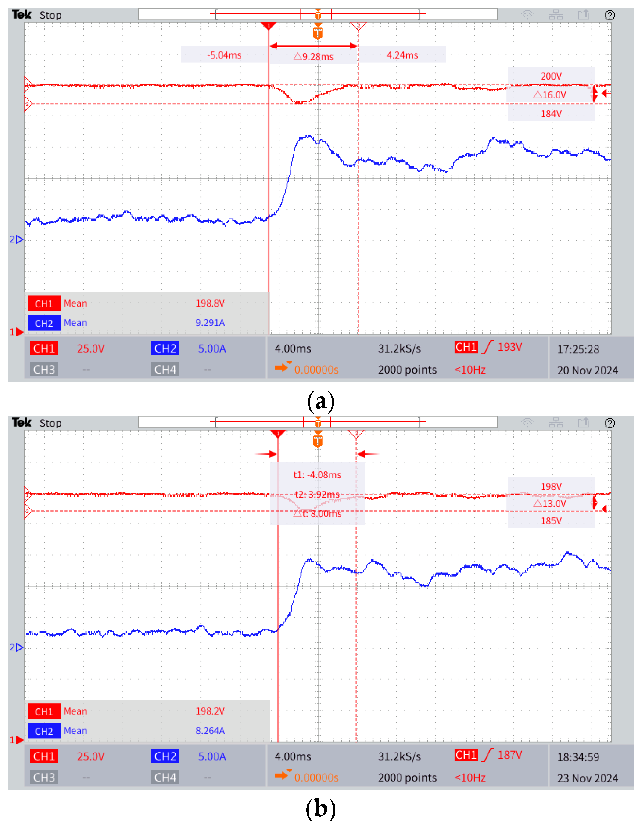
Under the conditions of an increasing DC side load, the oscilloscope measurement experimental waveform is shown in
Figure 19. Through an in-depth analysis of the experimental waveform results, it can be seen that, when the DC load gradually increases, the conventional PWM-PFM composite control can reach the steady-state setpoint in 9.55 milliseconds. However, the improved PWM-PFM composite control can reach the steady-state value after only 8 milliseconds. In addition, the overshoot of the conventional PWM-PFM composite control can reach a maximum of 13 V, while the overshoot of the improved PWM-PFM composite control is only 12 V. It can be clearly seen that the improved PWM-PFM composite control is significantly better than the conventional PWM-PFM composite control. Compared to the conventional composite control, the improved composite control has a faster settling speed and a lower overshoot.
5.3.2. The Load Reduction
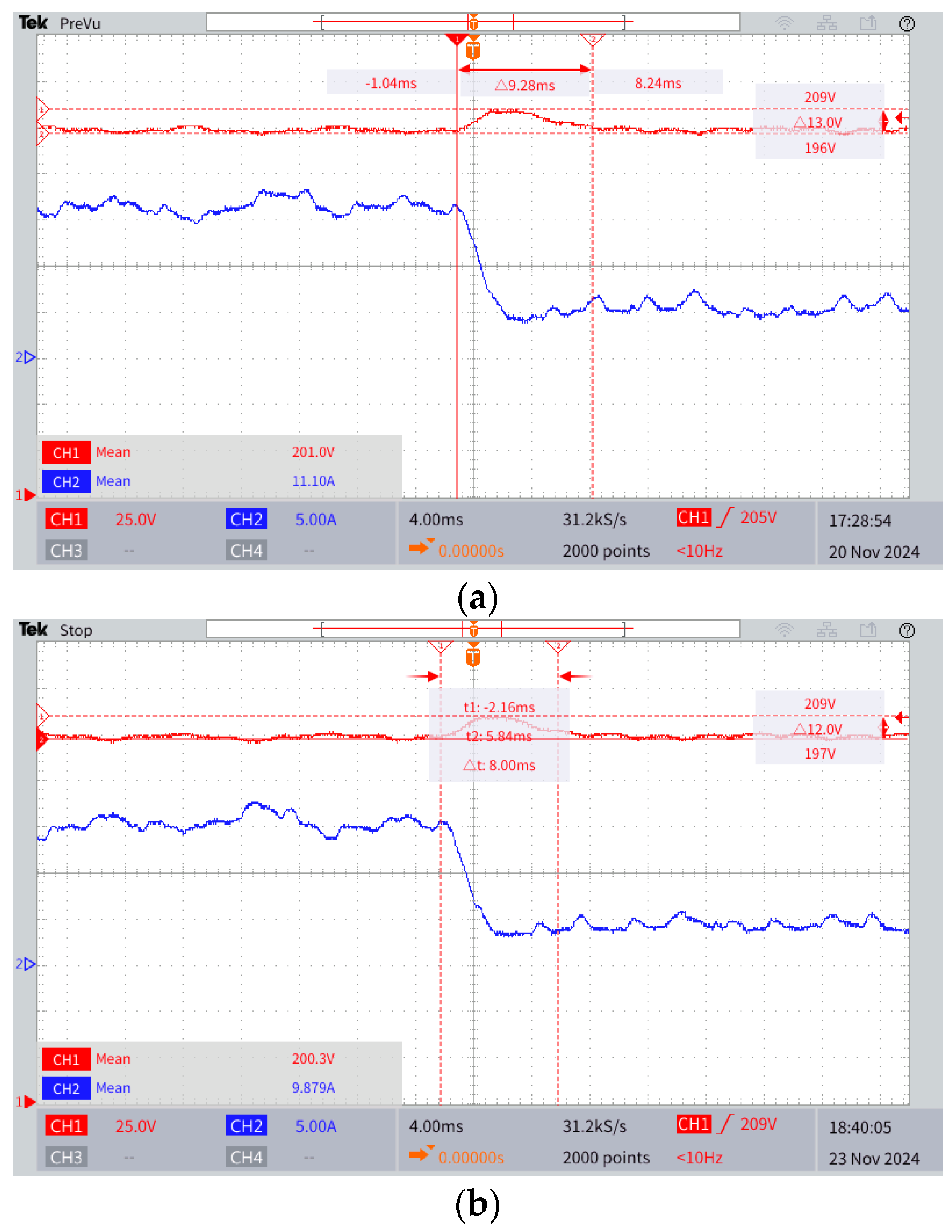
Under the conditions of decreasing DC side load, the oscilloscope measures the experimental waveform, as shown in
Figure 20. Through an in-depth analysis of the experimental waveform results, it can be seen that, when the DC load suddenly decreases, the conventional PWM-PFM composite control can reach the steady-state setpoint in 9.28 milliseconds. However, the improved PWM-PFM composite control can reach the steady-state value after only 7.5 milliseconds. In addition, the overshoot of the conventional PWM-PFM composite control can reach a maximum of 16 V, while the overshoot of the improved PWM-PFM composite control is only 13 V. It can be clearly seen that the improved PWM-PFM composite control is significantly better than the conventional PWM-PFM composite control. Compared to the conventional composite control, the improved composite control has a faster settling speed and a lower overshoot. Energy flows bidirectionally between ports via zero-voltage switching, achieving a 97.2% efficiency across 150–300 V input ranges, which is a 15% improvement over conventional cascaded designs.
5.4. ZVS Experimental Verification
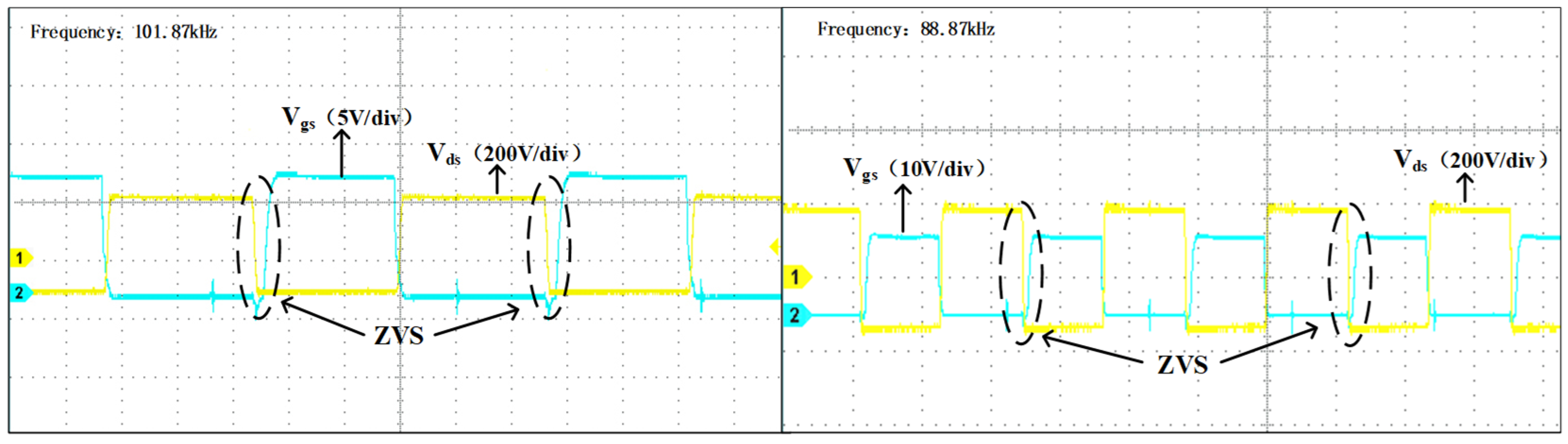
To validate the soft-switching performance of the converter, experimental characterization was conducted under both heavy-load and light-load conditions. As shown in
Figure 21, signal 1 (yellow line) is the drain source voltage, V
ds, of the switch, and signal 2 (blue line) is the drive signal V
gs. It can be seen from the figure that V
ds dropped to 0 before the arrival of voltage V
gs, and the converter can determine the ZVS of the switch tube. The soft switching characteristics of the switch under a light load and a heavy load are shown. The test shows that ZVS can be determined no matter what state the converter works in, achieving a wide range of soft switching characteristics.
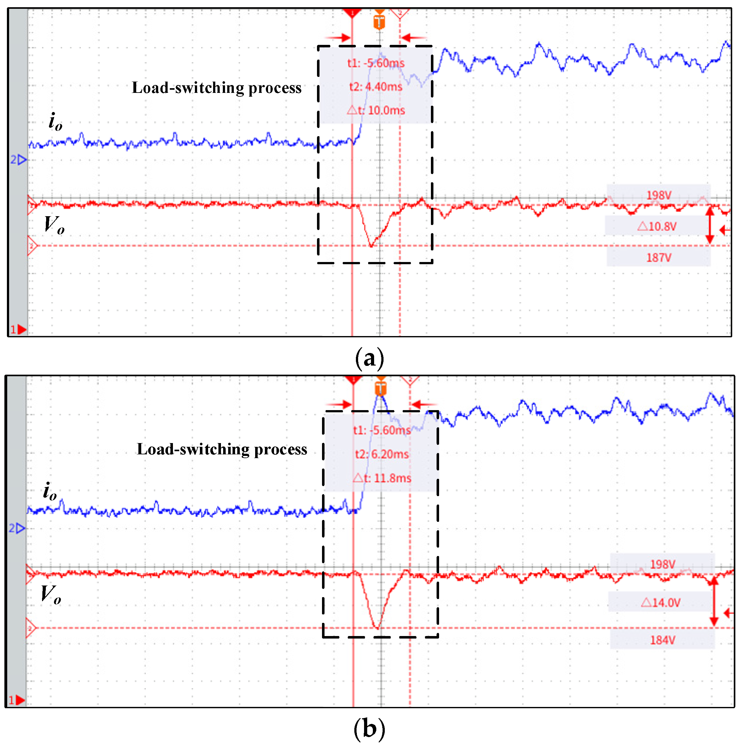
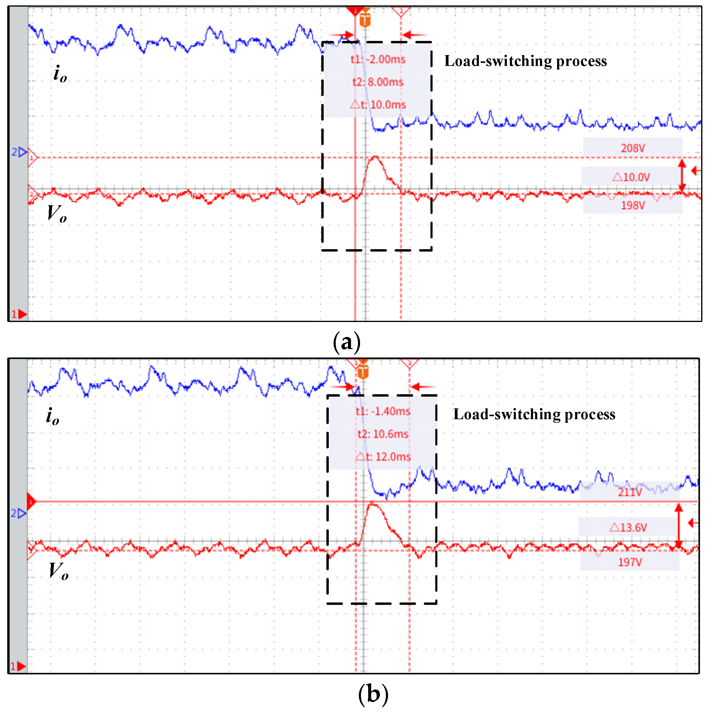
To assess the voltage regulation performance of the proposed converter, a load step-change test was conducted, comprising two comparative tests: one employing conventional PWM-PFM control, and the other utilizing an improved hybrid PWM-PFM strategy. Each test evaluated bidirectional load transients, including light-to-heavy and heavy-to-light load transitions. The experimental results are shown in the
Figure 22 and
Figure 23. From
Figure 22a, it can be observed that, during the light-load to heavy-load transition of the converter, the output current increases, while the output voltage experiences a brief transient dip before rapidly stabilizing. As shown in
Figure 22b, when transitioning from heavy-load to light-load conditions, the output current
decreases, and the output voltage
exhibits a short overshoot, before promptly recovering to its rated value. Under conventional PWM-PFM control, the converter demonstrates stabilization times of 11.8 ms and 12 ms for light-to-heavy and heavy-to-light load transitions, respectively, with corresponding voltage fluctuations of 14 V and 13.6 V. In contrast, the improved PWM-PFM control achieves reduced response times of 10 ms for both transition modes, accompanied by lower voltage fluctuations of 10.8 V and 10 V. Experimental results verify that the enhanced design effectively maintains voltage regulation during load transitions while improving dynamic response. Furthermore, the modified PWM-PFM control strategy enables dynamic power redistribution between ports without altering switching frequency. Through decoupled power regulation (coupling degree < 5%) and resonant tank optimization, this approach reduces control complexity while maintaining voltage ripple within ±2.5% under 20% load transient conditions.
6. Conclusions
This article presents a high-efficiency isolated three-port resonant converter tailored for DC microgrid applications, integrating a dual active bridge (DAB) and LLC resonant topology with hybrid PWM-PFM phase shift modulation. The proposed architecture synergizes interleaved buck/boost stages with the DAB-LLC structure to eliminate cascaded conversion losses inherent in conventional designs. Bidirectional power transfer between ports is enabled through zero-voltage switching (ZVS), achieving a peak efficiency of 97.2% across an extended input voltage range of 150–300 V, representing a 15% efficiency enhancement compared to conventional cascaded configurations. Also, an improved PWM-PFM phase shift control strategy is implemented to dynamically redistribute power across ports while maintaining fixed switching frequency operation. This approach decouples power regulation through resonant tank optimization, achieving voltage ripple suppression within ±2.5% under 20% load transients while significantly reducing control complexity. The converter further incorporates a switch-controlled capacitor network combined with adaptive frequency tuning to autonomously adjust resonant parameters, enabling a 1:2 voltage gain range without auxiliary circuitry. This innovation reduces implementation costs by 30% relative to dual-transformer solutions, demonstrating strong compatibility with heterogeneous DC microgrid architectures. In addition to detailed analysis, simulation and experimental results verify the effectiveness of the proposed concept.


