Article

Unified Inductor Type Based Linear Resonant Hybrid Converter for Wide Voltage Range Applications

1
School of Traffic & Transportation Engineering, Central South University, Changsha 410075, China
2
School of Electrical Engineering, Guangxi University, Nanning 530004, China
*
Author to whom correspondence should be addressed.
Energies 2025, 18(10), 2572; https://doi.org/10.3390/en18102572
Submission received: 8 April 2025 / Revised: 9 May 2025 / Accepted: 13 May 2025 / Published: 15 May 2025
(This article belongs to the Topic Power Electronics Converters, 2nd Edition)

Abstract

:
Pulse frequency modulation (PFM) is widely used in LLC resonant converters. However, in wide voltage applications, the switching frequency range is very wide, which affects the performance of magnetic components and filters. In order to achieve wide voltage gain in a narrow frequency range, this paper proposes a unified inductor type based linear resonant hybrid converter (UITBLRHC). The resonant inductor and excitation inductor are unified, and the resonant tank with equal inductance ratio is achieved. Hence, the output voltage can be adjusted within a very narrow frequency range. In addition, the parameters and operating modes of the two inductors are exactly the same. Therefore, the types of inductors can be reduced, and the magnetic flux and heat distribution between the two inductors are more uniform. Finally, an 800 W prototype was built. The proposed solution can achieve twice the voltage gain within a frequency range of 1.25 times. The experimental results prove the reliability and validity.

1. Introduction

Isolated DC/DC converters are employed in many application scenarios, such as energy storage systems, vehicle-to-grid applications, and renewable energy DC grid systems [1,2,3]. As one of the popular isolated DC/DC topologies, due to the advantages of soft switching characteristics, electrical isolation, high efficiency, and high power density, LLC resonant converter topology has received widespread attention in academia and industry [4,5,6]. For the traditional LLC resonant converter, pulse frequency modulation (PFM) is used to regulate the output voltage. When the switching frequency approaches the resonant frequency, the efficiency of LLC is higher [7]. However, for working scenarios with a wide voltage range, the switching frequency of the LLC converter needs to be varied over a considerably wide frequency range, which makes it more difficult to design the magnetic components and driver circuits [8,9].
In order to improve the voltage regulation capacity within a narrow switching frequency range, many improvement methods have been proposed based on the traditional LLC converter. The main improved schemes can be categorized into the following three: (1) Improving modulation strategies. (2) Reconfiguring the structure of the primary or secondary side. (3) Changing the topology of the resonant tank. For the aspect of improving the modulation strategy, some hybrid control strategies, such as PFM-phase-shift (PFM-PS) modulation [10,11] and pulse width modulation (PWM) with fixed frequency [12], are adopted. A hybrid modulation method is used in a dual-transformer-based LLC converter in [10]. Two different control strategies are used: PFM in normal operation and phase-shift control in hold-up-time operation. Similar to [10], two extra active switches are utilized in [11] to adjust the output voltage through phase shift angle. In [12], a PWM-controlled strategy is applied to widen the voltage gain range by controlling the duty cycle of the additional switch. Although they improve the gain range by some degree, the modulation strategies, driving logic, and circuit design become more complex. Pulse width modulation or phase shift modulation with fixed switching frequency is proposed in [13] and [14]. However, the voltage gain derivation and ZVS analysis are relatively complex. The mode switching control can effectively extend the voltage regulation range [15]. By changing the driving logic, the converter can be switched between full-bridge and half-bridge modes. Although this method can obtain more than twice the voltage gain, it is relatively difficult to achieve smooth mode switching. In [16], the voltage regulation capacity is optimized by periodically switching operation modes. Especially when running in burst mode, it can solve the overvoltage problem under light load. However, the equivalent frequency is reduced, and a larger filter is required.
The reconfigurable structure, like switching the resonant converter structure between full-bridge and half-bridge mode in [17] and arranging the configurable capacitors in parallel or series in [18], also contributes to enhanced voltage regulation capability. In [19], the semiactive variable-structure rectifier (SA-VSR) can operate in both voltage-doubler rectifier (VDR) mode and voltage-quadrupler rectifier (VQR) mode, which makes the output voltage range be doubled. Although mode switching can double the range of voltage gain, the modes’ smooth transition control is still a problem. And the number of components is usually more. In [20], the auxiliary switch is added. However, the complexity of the control and drive logic is increased.
In terms of the topology of the resonant tank, changing the equivalent parameters of the resonant tank or the combination method of resonant elements is a viable approach to broaden the voltage gain range. Neither additional active devices nor complex modulation strategies need to be introduced, which is very simple for practical implementation. A linear resonant hybrid bridge converter is proposed in [21]. By changing the position of the resonant inductor and adding the hybrid bridge, the converter can be divided into HG mode and LG mode. In [22], a CLL resonant converter with a secondary-side resonant inductor is proposed to remove the circulating current and reduce loss. Despite the fact that the number of their components is few, the types of inductors are still categorized into two different types, resonant inductors and excitation inductors, as in traditional LLC converters. Overall, in traditional LLC resonant topologies, it is necessary to supply two different inductors. Two types of inductors mean that inductors also require a separate design. A multi-transformer structure is adopted in [23]. The various operation configurations can achieve good conversion efficiency. However, the utilization of the auxiliary transformer is relatively low, which leads to a low power density. In [8,24], a variable inductor is used in a half-bridge variable magnetizing inductance-controlled LLC resonant converter. By changing the inductance value of the variable inductor, the inductance ratio can be altered to improve the gain capability. However, in order to change the inductance value, a variable inductor requires additional excitation to be applied to the corresponding winding.
In order to achieve wide voltage gain within a narrow frequency range and unify the types of inductors, this paper proposes a unified inductor type based linear resonant hybrid converter (UITBLRHC). The two inductors of the resonant tank operate in the linear resonant hybrid mode with the identical inductance values and working states. The detailed advantages are as follows:
  • The resonant inductor and excitation inductor are unified, and the resonant tank with equal inductance ratio is realized. The wide voltage gain can be achieved within a very narrow frequency range;
  • The type of inductor in the resonant tank is reduced. In addition, compared with the traditional LLC resonant converters, the magnetic flux and heat distribution are more uniform.
The rest of this paper is organized as follows. Section 2 presents the topology structure of the proposed UITBLRHC converter and its operation principle. In Section 3, the key characteristics of the proposed converter are analyzed. In Section 4, the design considerations and processes are discussed and shown. In Section 5, an 800 W prototype is built to verify the analysis, and the experimental results are presented. Furthermore, a comparison is made. Finally, Section 6 concludes this paper.

2. Proposed Topology and Operation Principle

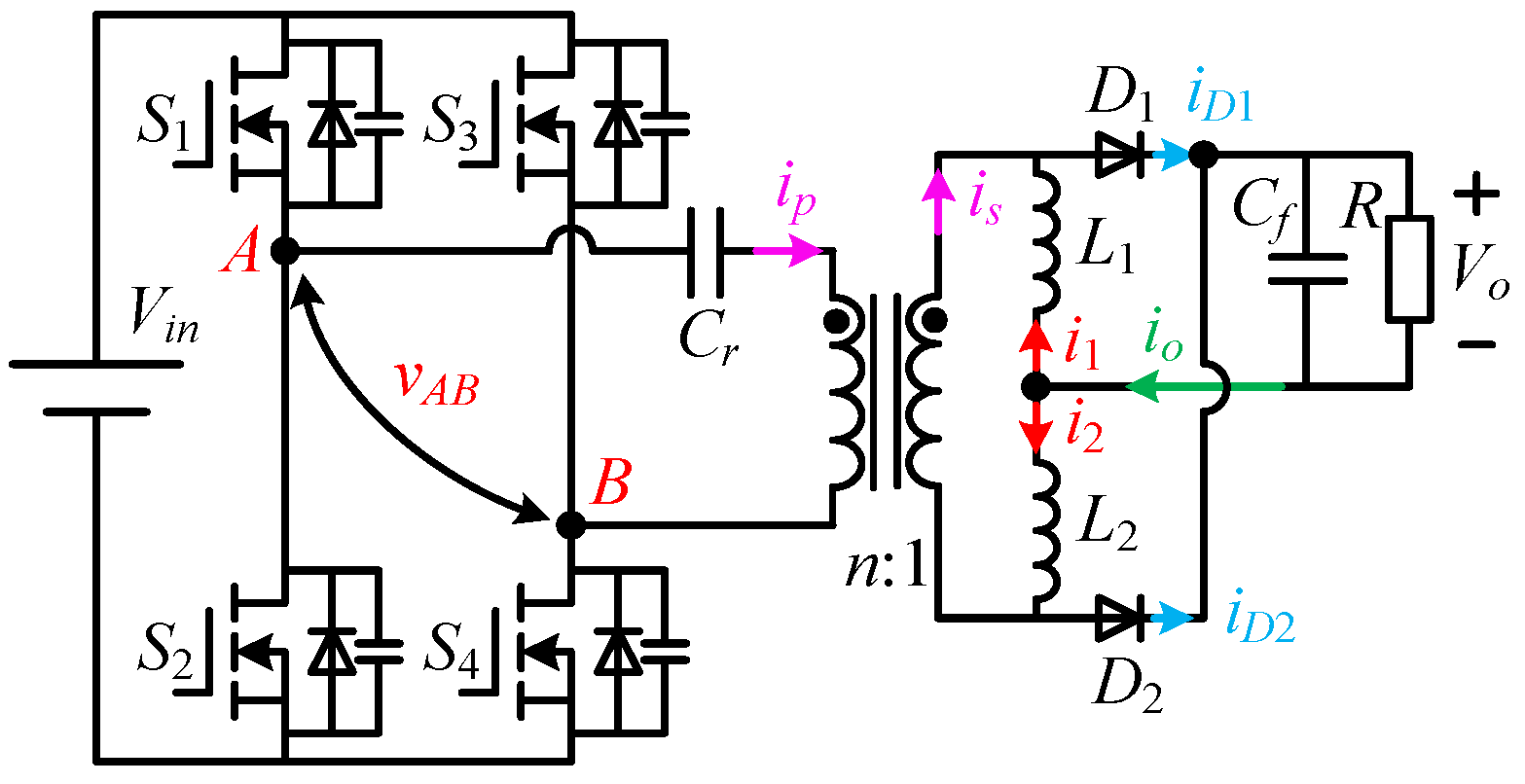
2.1. Topology of the Proposed UITBLRHC

The proposed unified inductor type based linear resonant hybrid converter (UITBLRHC) is shown in Figure 1. The input to the converter is a DC voltage source, Vin, and the output voltage is Vo. The primary side of the transformer is composed of a full-bridge structure with four switches. The midpoint A, B of each leg is connected to a resonant capacitor Cr in series with the power transformer. The secondary side is composed of two rectifier diodes; D1&D2; two linear resonant (L-R) inductors, L1&L2, with equal inductance value; and an output filter capacitor, Cf. The transformer turns ratio is defined as n: 1. The direction of the arrow in Figure 1 is the positive direction specified in this paper.
As shown in Figure 1, Cr resonates with two L-R inductors, L1 or L2, together constituting the resonant tank of the converter. Since L1 or L2 alternately presents linear or resonant characteristics, respectively, two L-R inductors have a unified function. The result is that the inductor types are unified and the equivalent inductance ratio L n = L r / L m equals one, making the converter obtain the capability of higher voltage gain.

2.2. Operation Principle

The typical operation waveform of the UITBLRHC converter is illustrated in Figure 2. Vin is the input voltage. iD1&iD2 are the currents of the rectifier diodes. i1&i2 are the currents of the L-R inductors. io is the output current. ip is the primary side current. Define that Lr is the equivalent resonant inductor and Lm is the equivalent excitation inductor. Define Ceq as the equivalent resonant capacitor converted to the secondary side. Thus, Lr, Lm, Ceq, and the series-resonant frequency fr can be expressed as follows:
L r = L m = L 1 = L 2 C e q = C r × n 2 f r = 1 / 2 π L r C e q
There are a total of eight stages in a complete operation period. Since the first and second half cycles are completely symmetrical, only the first half of the cycle will be analyzed as an example. The equivalent circuits of each stage are illustrated in Figure 3.
Stage 1 [t0, t1] [see Figure 3a]: Before t0, S2&S3 are ON. i1 and i2 are equal in amplitude and opposite in polarity. Cr is in ternary resonance with both L1 and L2. Stage 1 begins at t0 when S2&S3 are turned OFF and D1 is turned ON. It should be noted that Stage 1 is within the deadband of S1S4. Since the polarity of ip is negative, ip charges the output capacitors Coss2,3 of S2&S3 and discharges Coss1,4. When the voltages across Coss1,4 are discharged to 0, the body diodes of S1&S4 are able to conduct, preparing for ZVS turn ON of S1&S4. ir, vCr, im and ip can be expressed as follows:
i r ( t ) = i 2 ( t ) = I m cos ω r ( t t 0 ) + V i n / n V o V C r 0 / n Z r sin ω r ( t t 0 ) v C r ( t ) = V i n n V o + Z r I m sin ω r ( t t 0 ) V i n n V o V C r 0 n cos ω r ( t t 0 ) i m ( t ) = i 1 ( t ) = I m V o L m t t 0 i p ( t ) = i r ( t ) / n = i 2 ( t ) / n
where −Im is the initial value of the resonant current at t0, and VCr0 is the initial value of the voltage at t0, ω r = 1 / L r C e q , Z r = L r / C e q .
Stage 2 [t1, t2] [see Figure 3b]: As the body diodes conduct, the voltages across both S1 and S4 are 0. At t1, S1&S4 are turned ON with ZVS. The input and output port voltages of the resonant tank remain both constant; hence, ir, vCr, im, and ip have the same expression formulas as stage 1.
It should be noted that ir is defined as the current of the equivalent resonant inductor. For example, L2 is employed as a resonant inductor in stages 1 and 2, resulting in i2 and ir being identical. And im is defined as the current of the equivalent excitation inductor. Due to the voltage across L1 being clamped by −Vo, L1 is utilized as the excitation inductor, and im is equal to i1.
Stage 3 [t2, t3]: At t2, since the resonant current becomes positive, the polarity of ip also turns positive. Apart from that, the working condition is the same as Stage 2. During this stage, im will decrease under the effect of −Vo and eventually reach a negative peak.
Stage 4 [t3, t4] [see Figure 3c]: At t3, i1 and i2 are again equal in amplitude and opposite in polarity; thus, io and iD1 are identical and equal to 0. D1 is turned OFF with ZCS. Cr will be in ternary resonance with both L1 and L2 during this stage. Because of D1 being OFF, the load is supplied by Cf. ir, vCr, im, and ip can be written as follows:
i r ( t ) = I m 1 cos ω r 2 ( t t 3 ) + V i n / n V C r 1 / n 2 Z r sin ω r 2 ( t t 3 ) v C r ( t ) = V i n n + 2 Z r I m 1 sin ω r 2 ( t t 3 ) V i n n V C r 1 n cos ω r 2 ( t t 3 ) i m ( t ) = i r ( t ) = i 1 ( t ) = i 2 ( t ) i p ( t ) = i r ( t ) / n
where Im1 is the initial value of the current at t3 and VCr1 is the initial value of the voltage at t3.

3. Characteristics of the UITBLRHC

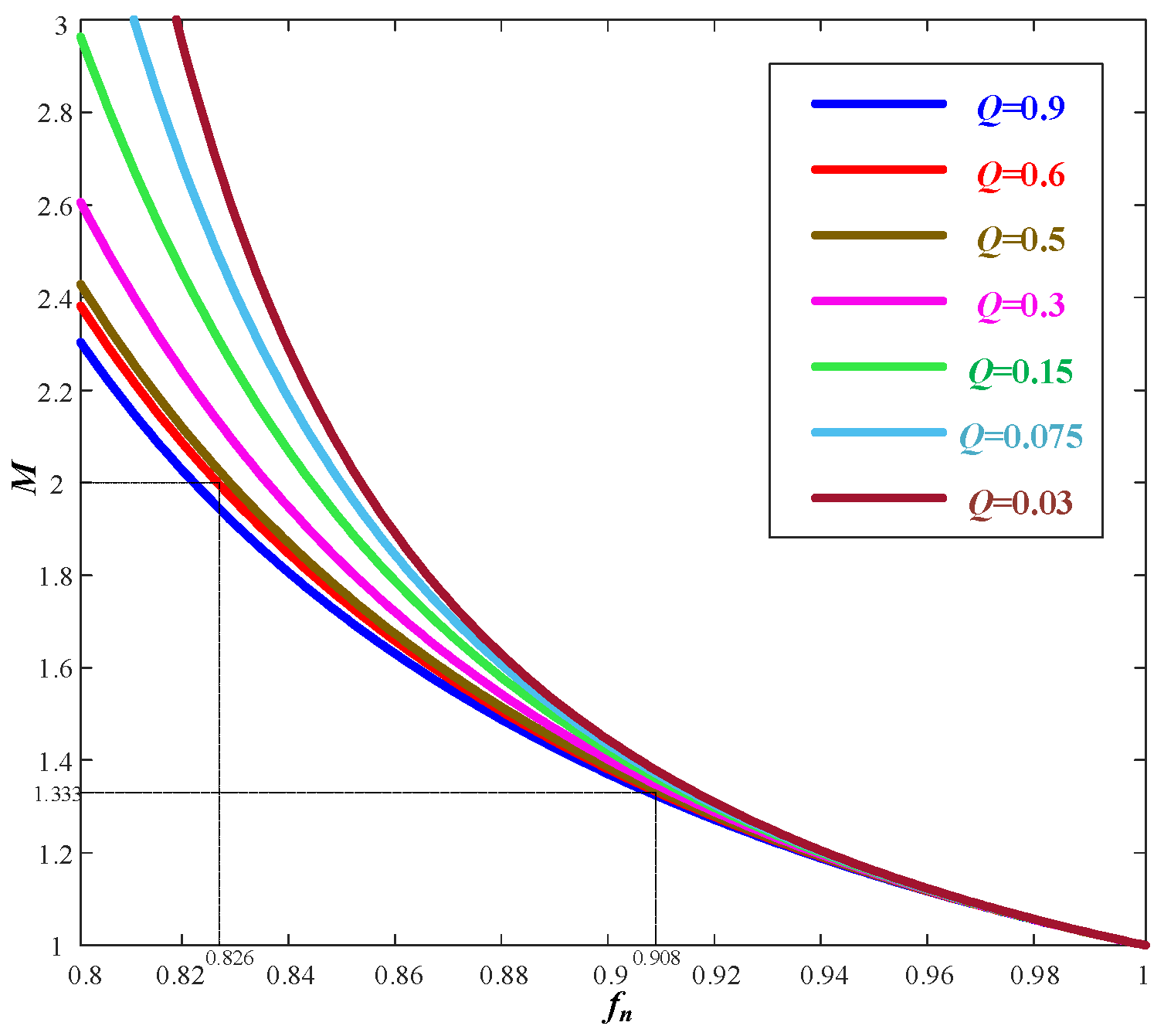
3.1. Voltage Gain Characteristic

Generally, fundamental harmonic approximation (FHA) is used in resonant converters to analyze the voltage gain characteristic. However, due to the high harmonic content of the current, FHA will lose accuracy. Therefore, time domain analysis (TDA) is applied in UITBLRHC. The normalized voltage gain of the resonant tank is defined as follows:
M = V o V i n / n = n V o / V i n
To simplify the calculation, the phase is used to represent the time:
θ = ω r t θ 0 = ω r t 0 = 0 θ 1 = ω r t 3 θ 2 = ω r t 4
Therefore, Equations (2) and (3) can be written as follows:
( 0 θ θ 1 ) i r ( t ) = I m cos θ + V i n / n V o V C r 0 / n Z r sin θ v C r ( t ) = V i n n V o + Z r I m sin θ V i n n V o V C r 0 n cos θ i m ( t ) = I m V o ω r L m θ
( θ 1 < θ θ 2 ) i r ( t ) = I m 1 cos θ θ 1 2 + V i n / n V C r 1 / n 2 Z r sin θ θ 1 2 v C r ( t ) = V i n n + 2 Z r I m 1 sin θ θ 1 2 V i n n V C r 1 n cos θ θ 1 2 i m ( t ) = i r ( t )
The capacitor voltages and inductor currents are always continuous in two adjacent stages. The voltage and current are symmetrical for the half cycle. Thus, the boundary conditions can be obtained:
I m = i r ( t 4 ) = i r ( t 0 ) V C r 0 = v C r ( t 0 ) = v C r ( t 4 ) I m 1 = i r ( t 3 ) = i m ( t 3 )
When the output voltage is Vo and the output power is Po, the equivalent load R = V o 2 / P o and the output current Io can be expressed as follows:
I o = V o R = V o π 2 R a c / 8 = 8 Q V o Z r π 2
where Rac is defined as R a c = 8 R / π 2 . And Q is defined as Q = Z r / R a c , which can indicate light or heavy load conditions.
Meanwhile, io is also the sum of i1 and i2, and averaging io over the half cycle is Io, which yields the following:
I o = i o ¯ = 1 T s / 2 t 0 t 4 [ i 1 ( t ) + i 2 ( t ) ] d t
Since i 1 = i 2 during [t3, t4], the equation can be reduced to the following:
8 Q V o 2 Z r π 2 f s = t 0 t 3 i 1 ( t ) d t + t 0 t 3 i 2 ( t ) d t
During [t0, t3], i2 is equivalent resonant current ir, which charges and discharges the resonant capacitor Cr:
t 0 t 3 i 2 ( t ) d t = t 0 t 3 i r ( t ) d t = C e q ( V c r 1 n V c r 0 n )
And i1 is equivalent to the excitation current, im. As shown in Figure 4, the integral of im over t0 to t3 is the area of the green rectangle minus the area of the yellow triangle, so the following can be deduced:
t 0 t 3 i 1 ( t ) d t = t 0 t 3 i m ( t ) d t = I m ( t 3 t 0 ) V o L m ( t 3 t 0 ) ( t 3 t 0 ) 2
Define the base values of the normalization parameters as follows:
V b a s e = V i n n ;   Z b a s e = Z r ;   I b a s e = V b a s e Z b a s e ;
The normalized variables are calculated by the following equation:
V x N = V x V b a s e ;   I x N = I x I b a s e ;
where the subscript x denotes the corresponding original variable, and xN denotes the normalized variable.
Therefore, by combining Equations (11)–(13) and normalizing the expression, the relationship between the charging of the resonant capacitor and the resonant current can be derived as follows:
V C r 1 N V C r 0 N + I m N θ 1 M θ 1 2 2 = 8 M Q θ 2 π 2
Combe Equations (4)–(8) and (14)–(16) and define the normalized frequency fn as f n = f s / f r . By normalizing all the relevant equations, the system of Equation (17) can be obtained:
I m N = I m 1 N cos θ 2 θ 1 2 + 1 V C r 1 N 2 sin θ 2 θ 1 2 V C r 0 N = ( 1 V C r 1 N ) cos θ 2 θ 1 2 1 2 I m 1 N sin θ 2 θ 1 2 M θ 1 I m N = I m N cos θ 1 + ( 1 M V C r 0 N ) sin θ 1 V C r 1 N = ( 1 M ) I m N sin θ 1 ( 1 M V C r 0 N ) cos θ 1 I m 1 N = I m N cos θ 1 + ( 1 M V C r 0 N ) sin θ 1 V C r 2 N = 1 + 2 I m 1 N sin θ 2 θ 1 2 ( 1 V C r 1 N ) cos θ 2 θ 1 2 ( V C r 1 N V C r 0 N ) + I m N θ 1 M θ 1 2 2 = 8 M Q θ 2 π 2 θ 2 = ω r t 4 = ω r T s / 2 = π / f n
Since the analytical solution for the voltage gain M is hard to find, the numerical solution of the system of Equation (17) is obtained with the help of computerized mathematical tools, and the gain curve is given by the graphical representation method. Figure 5 plots the normalized voltage gain versus the normalized frequency fn under different loads. It can be seen that the proposed UITBLRHC converter can achieve a wide voltage gain range in a narrow frequency range.

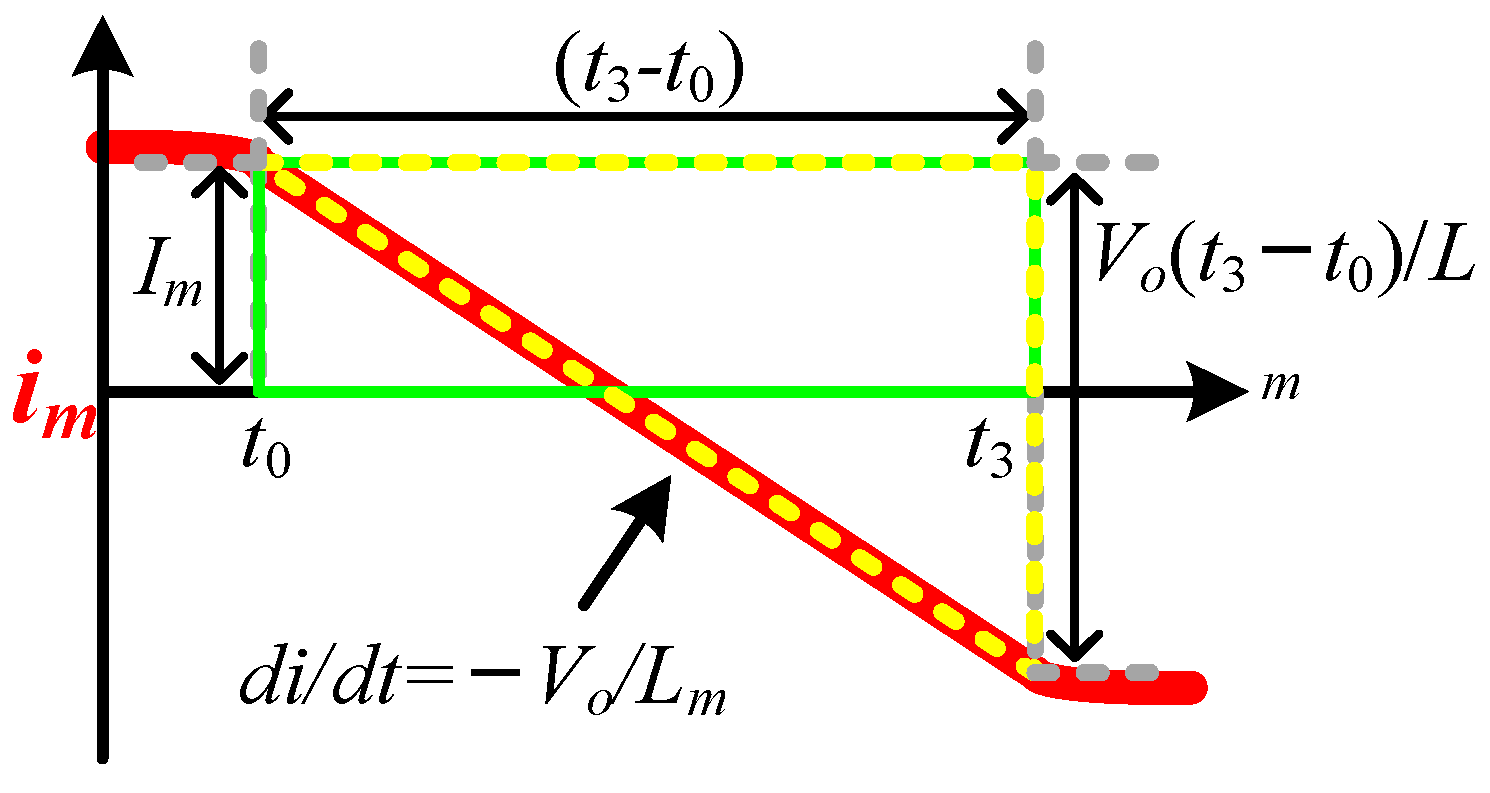
3.2. Soft Switching Performance

According to the operation principle in the previous paper, due to being in the discontinuous conduction mode (DCM) at f s < f r , ZCS turn OFF can be realized for both secondary-side rectifier diodes.
Although theoretically, ZVS turn ON for all switches on the primary side can be achieved naturally since the impedance of the resonant tank is inductive. However, in practice, to achieve ZVS turn ON in the deadband of S1S4, it is necessary to ensure that the excitation current discharges the output capacitors Coss to 0. Therefore, a large excitation current, Im, helps the ZVS implementation. Given that the duration of the deadband is small enough, the resonant tank is approximated as a current source, Im. The equivalent excitation current Im can be approximately expressed as follows:
I m = V o 4 L m f s
Considering the charge relationship of the output capacitors, it is essential to satisfy the following:
n I m t d e a d 4 C o s s V i n 0
Combing Equations (18) and (19), the ZVS condition can be obtained:
t d e a d 16 L m V i n f s C o s s n V o
It should be noted that this current is also the switch-off current of the complementary switches at the same time. Thus, the current should not be too large, or it will greatly increase the switch-off loss. Consequently, there is a trade-off to be considered in the actual design.

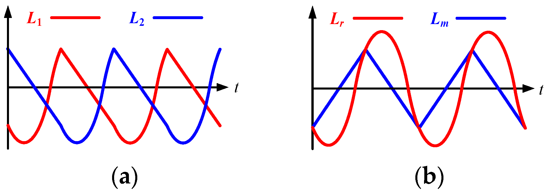
3.3. Magnetic Flux Analysis

The current waveforms of unified and non-unified resonant tanks are shown in Figure 6. It can be seen that for unified inductor type L-R inductors, the excitation current waveforms of L1 and L2 are the same, except for a 180-degree difference in phase. However, both amplitudes and waveforms are different for two types of separate inductors. From this perspective, the flux variations of two L-R inductors are the same, whereas the flux distribution of two types of separate inductors is not homogeneous, manifesting as higher in one and lower in the other.
The results of finite element analysis (FEA) simulations for the magnetic flux distribution are compared in Figure 7. Apart from the different waveforms of winding excitation, the parameters of the two structures are identical. The relation between the magnetic flux variations in the three cases is as follows:
Δ B L r > Δ B L - R > Δ B L m
where Δ B L r , Δ B L - R , and Δ B L m are the flux variations of the L-R inductor, resonant inductor, and excitation inductor, respectively. When using the same core and winding, and both inductors are of the same inductance value, the flux distribution between two L-R-type inductors will be more uniform compared to the combination of an individual resonant inductor and an individual excitation inductor. Since the hysteresis loss is mainly caused by the maximum magnetic flux density Bm, the L-R-type inductors will also have a more uniform loss distribution.

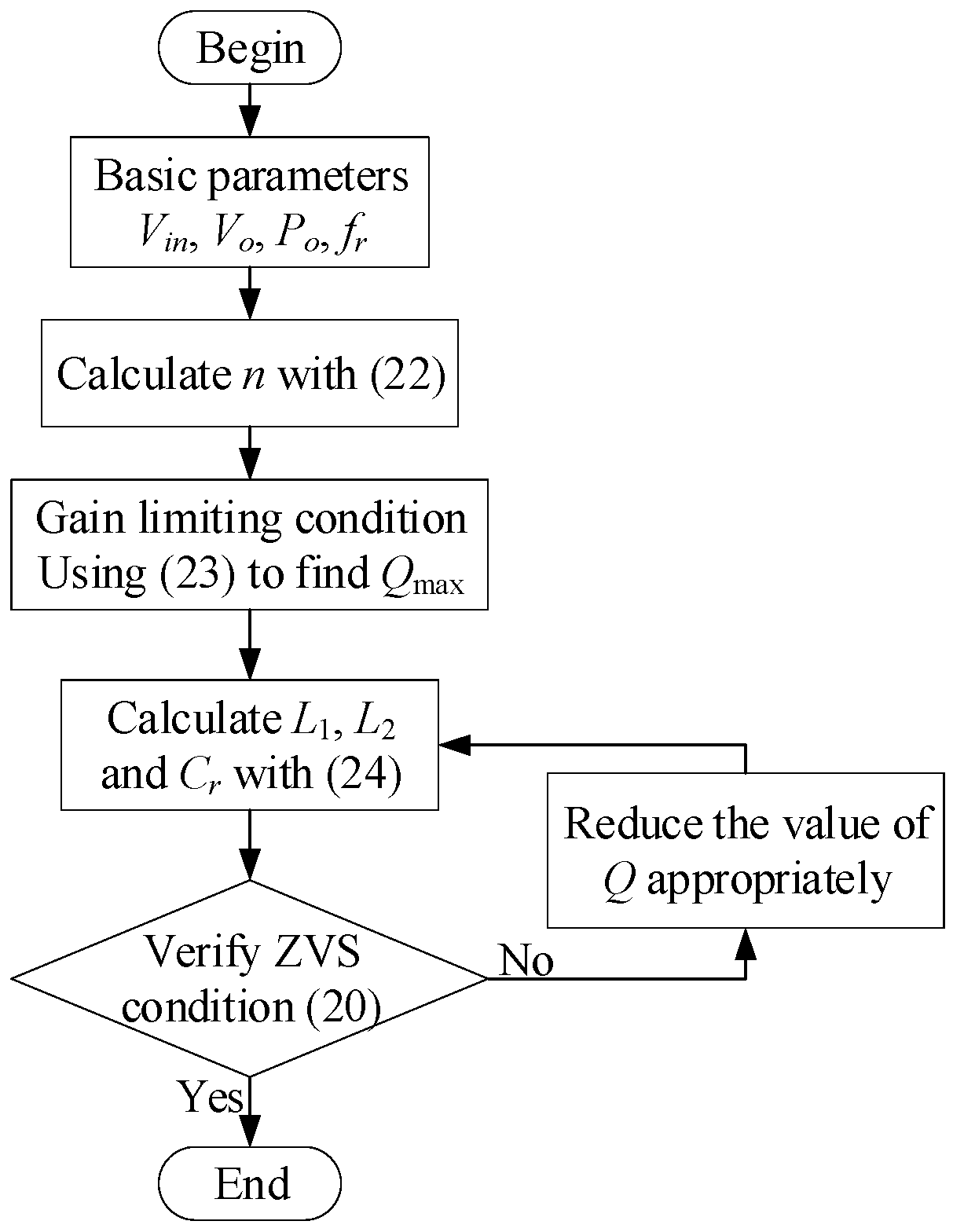
4. Proposed Converter Design Considerations

Figure 8 shows the overall design flowchart for the proposed UITBLRHC. To demonstrate the design process in detail, an example of the design of an 800 W experimental prototype is also used in this section. The circuit parameters are listed as follows: input voltage Vin = 240–480 V, output voltage Vo = 110 V, rated output power Po = 800 W, and resonant frequency fr = 150 kHz.

4.1. Turns Ratio of the Transformer

Taking the resonant point as the normal operating point, it corresponds to the case of maximum input voltage. Defining Vnorm = 480 V as the base input voltage at unit voltage gain. Hence, based on (4), the turns ratio n of the transformer can be designed as follows:
n = V n o r m V o
In the practical design, the number of coil turns must be an integer in order to facilitate the fabrication of the transformer.

4.2. Factor Q

Although the FHA method loses some accuracy, it is still widely used in the design of resonant converters due to its simplicity. Only two degrees (Q and Ln) should be considered. Once both of them are selected, the parameters of the resonant tank can be directly solved. Therefore, this paper still adopts the FHA method to obtain the resonant parameters.
Since two identical L-R inductors serve as a resonant inductor and an excitation inductor, respectively, the inductor ratio Ln equals one. Consequently, there is only one degree that needs to be chosen. Given that the input voltage range is 240–480 V, the maximum voltage gain, therefore, is 2. The maximum value of the factor Q is determined by the following equation:
Q max = 1 L n M max L n + M max 2 M max 2 1
It is worth noting that the FHA method will have a large error considering that the higher harmonic components account for more when the resonant converter operates away from the resonant frequency. Therefore, a certain margin should be left in the consideration of the maximum value of the voltage gain.

4.3. Resonant Tank

Once the factor Q is determined, the resonant parameters can also be obtained. The resonant parameters can be expressed as follows:
L 1 = L 2 = 4 Q V n o r m 2 π 3 n 2 f r P o C r = π P o 16 Q f r V n o r m 2
After calculating the resonant parameters, it is also necessary to verify that the ZVS can be realized by substituting the inductance value into relation (20). Since a margin was left for the choice of factor Q in the previous section, the value of Q can be appropriately reduced if relation (20) is not satisfied.

5. Experimental Verification and Comparison

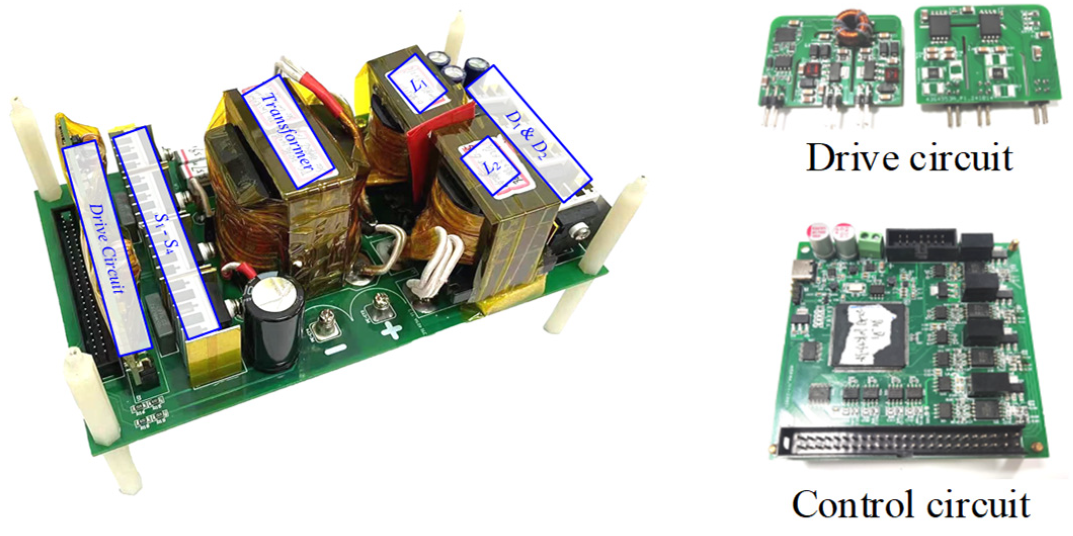
5.1. Experimental Prototype

An 800 W experimental prototype is built as shown in Figure 9, and relevant experiment tests are conducted on this platform to verify the validity of the proposed UITBLRHC. According to Formulas (22)–(24), the key parameters of the converter can be determined. The detailed parameters of UITBLRHC are listed in Table 1.

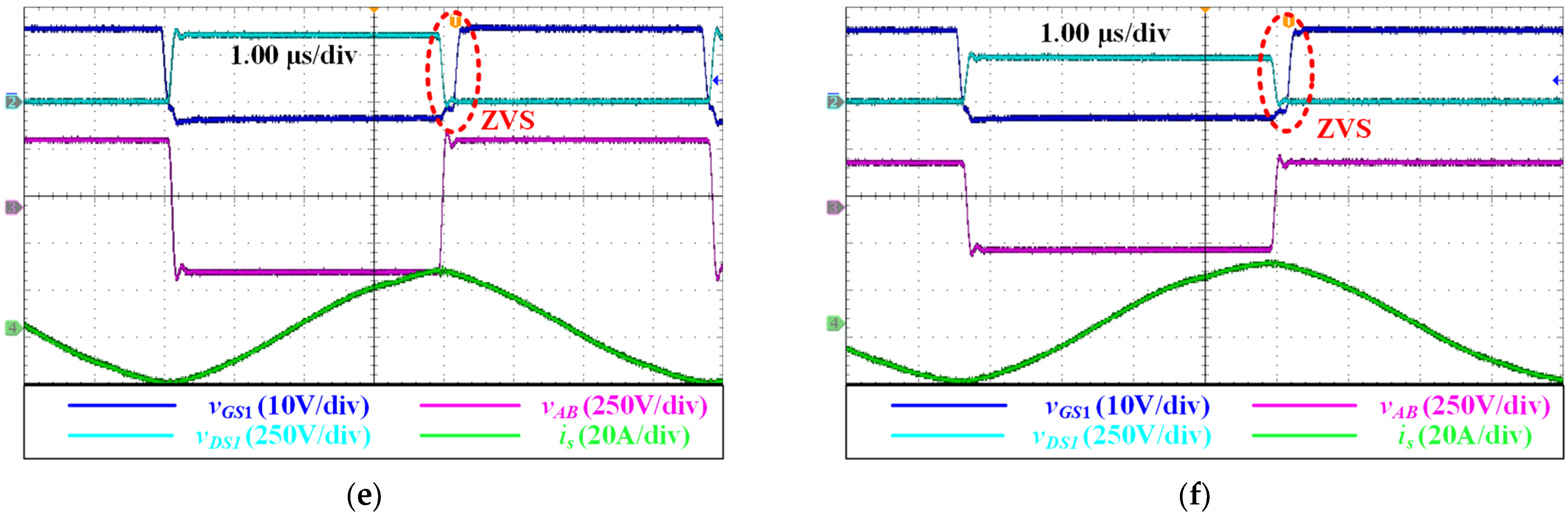
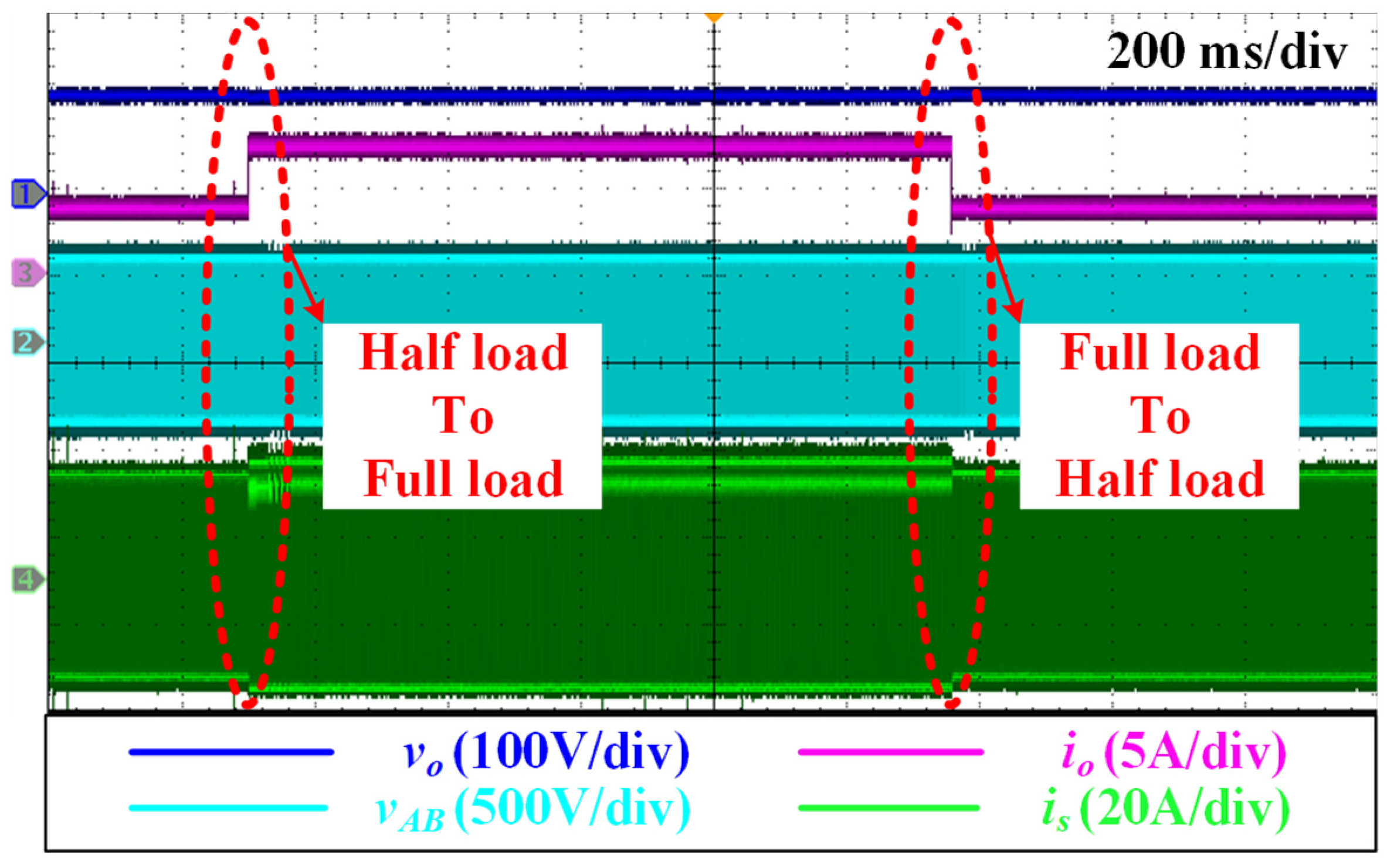
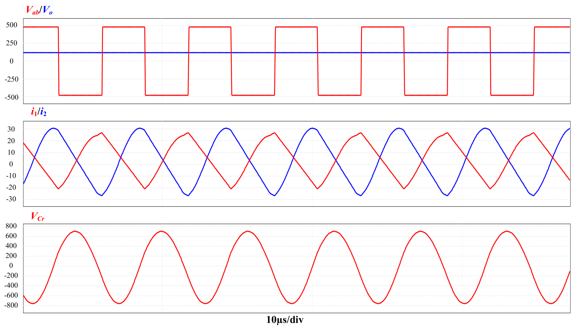
5.2. Experimental Results and Waveforms
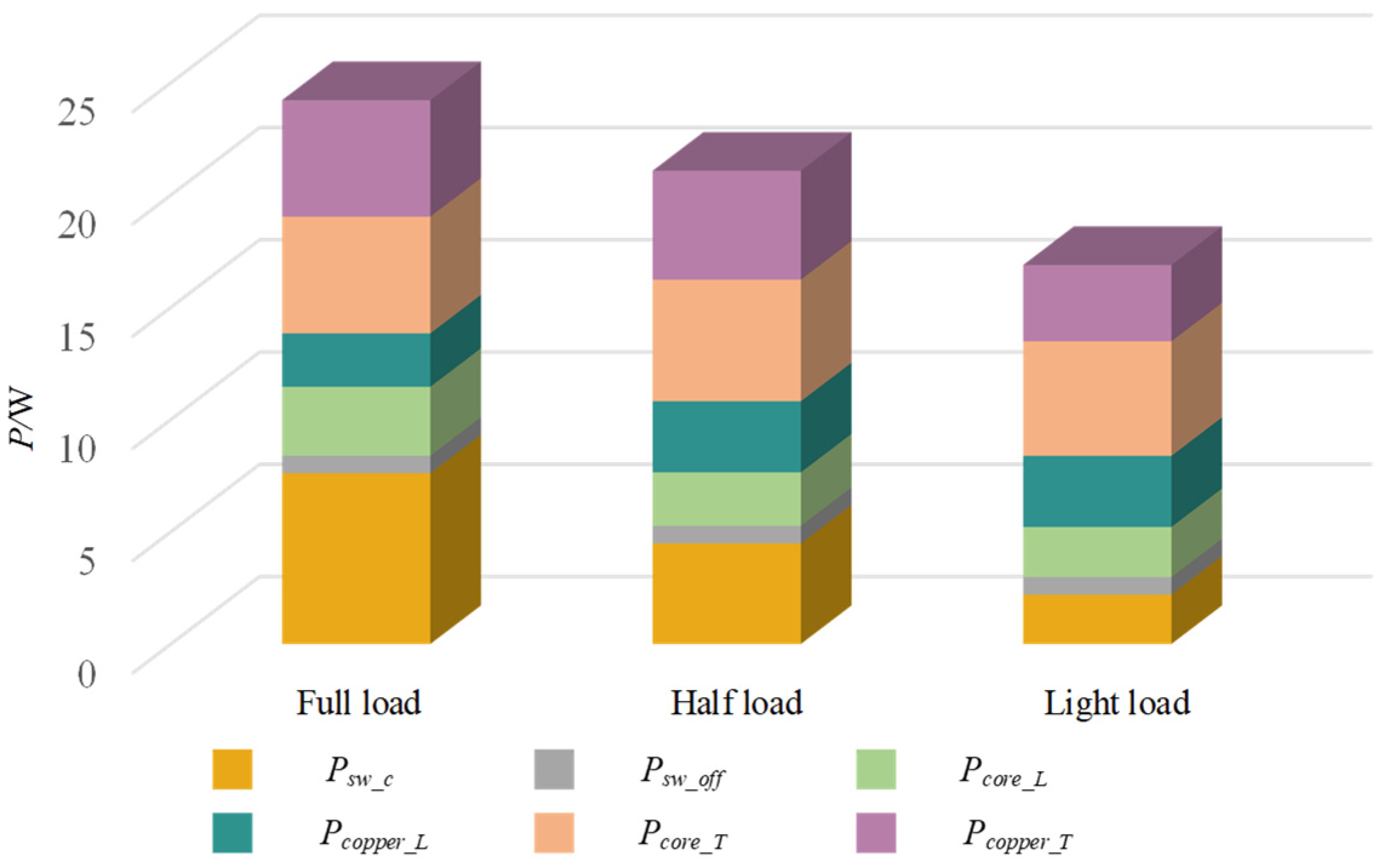
The steady-state working waveforms of the proposed UITBLRHC under different input voltages are shown in Figure 10. Over a wide input voltage range of 240–480 V, the proposed UITBLRHC can operate effectively to maintain a constant output voltage. The case of different input voltages can be represented by the amplitude of vAB. Additionally, the inductor currents iL1 and iL2 alternate between sinusoidal and linear, demonstrating linear resonant features. It is worth noting that from the voltage gain curves in Figure 5, the theoretical normalized frequencies are 1, 0.908, and 0.826 (with corresponding switching frequencies of 150, 136.2, and 123.9 kHz) for voltage gains of 1, 1.33, and 2, respectively. Meanwhile, the practical switching frequencies are 150, 136, and 124 kHz for identical output voltage when input voltages are 480, 360, and 240 V, respectively, which can match the theoretical values. This correspondence effectively proves the accuracy of the voltage gain analysis discussed in Section 3, based on the time-domain method.
Since the driver signals of S1&S4 or S2&S3 are identical and the duty cycle is fixed at 50%, the ZVS realization is the same for both bridge arms on the primary side. Hence, the ZVS waveforms of only one bridge arm (S1&S2) are shown in Figure 11. From Figure 11a–c, it can be seen that the drain source voltage vDS of switches is reduced to zero before the rising of the driver signal under different input voltages. Consistent with theoretical analysis, all switches can achieve ZVS turn ON. Apart from this, Figure 11d–f also gives the ZVS realization for different load cases. It can be seen that even under light load conditions, UITBLRHC is able to achieve ZVS turn ON.
The dynamic waveform of load switching is shown in Figure 12. When the output current changes within twice the range (3.6–7.2–3.6 A), the output voltage is maintained at 110 V. Therefore, the proposed UITBLRHC has good performance in a wide-range application. From the dynamic waveform of switching between half load and full load, when the load change occurs, the output voltage can also be adjusted rapidly and held at 110 V.
The curves of measured conversion efficiency for different output power levels under input voltages of 240, 360, and 480 V are shown in Figure 13. Due to the soft switching capability, the proposed UITBLRHC has good performance. The peak efficiency can reach 95.85%.

5.3. Loss Breakdown

The losses breakdown of the theoretical calculation is shown in Figure 14. For the proposed UITBLRHC, all the MOSFETs are turned on with ZVS, and all the diodes are turned off with ZCS. Hence, turning-on losses of MOSFETs and reverse recovery losses of diodes are zero. The overall losses can be divided into seven parts, namely conduction loss, switches turn-on loss, switches turn-off loss, inductor core loss, inductor copper loss, transformer core loss, and transformer copper loss. Among them, the conduction loss of switches and the copper loss of magnetic components are relatively high. The overall trend is basically consistent with the measured results. And it can be seen that efficiency is indeed higher under heavy loads, which is due to the large circulating current in the converter during light loads.

5.4. Inductor Difference Analysis

In the experimental prototype, L1 and L2 are 6.55 and 6.48, respectively. When the inductance difference is low, the inductor current waveform is symmetrical and the power is evenly distributed, as shown in the experimental waveform in Figure 10.
When the inconsistency between inductors increases, the characteristics of the converter will also be affected to a certain extent. The full load operation simulation results with a 20% inductance difference are shown in Figure 15. Under steady-state conditions, the difference in RMS value of inductor currents is approximately 17%.

5.5. Comparison

The proposed UITBLRHC is compared here with the conventional full-wave rectifier LLC converter since they are both resonant converters and PFM is used to regulate the output voltage for both of them.
For LLC, the magnetizing inductor of the transformer is typically utilized as the excitation inductor Lm. Therefore, the value of inductance ratio Ln is generally at least greater than 3, which limits the voltage gain capability of LLC topology. In contrast, due to inductor unification, UITBLRHC with an equivalent inductance ratio of 1 is more suitable for application scenarios in a wide voltage range.
While LLC can achieve an inductance ratio of 1 by using an external excitation inductor and resonant inductor, utilizing unified L-R-type inductors leads to better balance in terms of magnetic flux, losses, and thermal distribution, as analyzed earlier in Section 3. And the proposed UITBLRHC is simpler to design as it only needs to design one type of inductor.
The transformer in full-wave rectifier LLC topology has a central tap, with each secondary winding only operating for half a cycle while the other winding does not transfer power simultaneously. This alternating operation mode of two windings leads to a waste of winding utilization. Additionally, the structure with a central tap also makes manufacturing more complex. Compared with the former, the transformer in UITBLRHC does not require a central tap. This design is not only simpler to manufacture but also allows the secondary winding to operate throughout the entire cycle, resulting in improved utilization of the winding.
The proposed UITBLRC is compared with the other resonant topologies, as shown in Table 2. Compared with other wide voltage range resonant topologies, the proposed converter has fewer components. Moreover, the voltage regulation range is wide, which can be realized in a narrow frequency range. In terms of magnetic components, the transformer does not require a center tap, and there is only one inductor type in the proposed topology, simplifying the design of the magnetic components.

6. Conclusions

In this paper, a UITBLRHC converter is proposed and explored. The proposed converter uses two types of inductors as unified L-R-type inductors. Therefore, because of a low equivalent inductance ratio, a wide voltage gain range over a narrow switching frequency range can be achieved. Based on time-domain analysis, the proposed converter is suitable for wide voltage range application due to its high voltage gain characteristic. In addition, under the unified inductor type, the magnetic flux and heat distribution of the L-R inductors are more balanced. Compared to a full-wave rectifier, the transformer optimizes its winding utilization and eliminates the center tap, simplifying the design. Experimental results verify the effectiveness and the feasibility of the proposed topology.

Author Contributions

Conceptualization, J.X., H.W. and B.L.; methodology, J.X. and H.W.; writing—original draft preparation, J.X. and H.W.; writing—review and editing, J.X. and B.L. All authors have read and agreed to the published version of the manuscript.

Funding

This work was supported in part by the National Natural Science Foundation of China under Grants 52407232 and 52377172, in part by the Key Research and Development Program of Hunan Province under Grant 2024JK2013, and in part by the Transportation Operation Subsidy Project of Guangxi Key Laboratory of International Join for China-ASEAN Comprehensive Transportation in 2021, No. 21-220-21.

Data Availability Statement

The original contributions presented in the study are included in the paper, further inquiries can be directed to the corresponding author.

Conflicts of Interest

The authors declare no conflicts of interest.

References

  1. Li, L.; Xu, G.; Sha, D.; Liu, Y.; Sun, Y.; Su, M. Review of Dual-Active-Bridge Converters with Topological Modifications. IEEE Trans. Power Electron. 2023, 38, 9046–9076. [Google Scholar] [CrossRef]
  2. Li, L.; Su, M.; Xu, G.; Jiang, L.; Liu, Y. A Soft-Switched Semi Dual Active Half Bridge Converter with Voltage Match Trapezoidal Modulation Control. IEEE Trans. Circuits Syst. II Express Briefs 2024, 72, 303–307. [Google Scholar] [CrossRef]
  3. Rocha, J.; Amin, S.; Coelho, S.; Rego, G.; Afonso, J.L.; Monteiro, V. Design and Implementation of a DC–DC Resonant LLC Converter for Electric Vehicle Fast Chargers. Energies 2025, 18, 1099. [Google Scholar] [CrossRef]
  4. Yin, M.; Luo, Q. Stepwise Multi-Objective Parameter Optimization Design of LLC Resonant DC-DC Converter. Energies 2024, 17, 1919. [Google Scholar] [CrossRef]
  5. Yang, B.; Lee, F.; Zhang, A.; Huang, G. LLC resonant converter for front end DC/DC conversion. In Proceedings of the APEC 2002—Applied Power Electronics Conference and Exposition, Dallas, TX, USA, 10–14 March 2002; pp. 1108–1112. [Google Scholar]
  6. Beiranvand, R.; Zolghadri, M.R.; Rashidian, B.; Alavi, S.M.H. Optimizing the LLC–LC Resonant Converter Topology for Wide-Output-Voltage and Wide-Output-Load Applications. IEEE Trans. Power Electron. 2011, 26, 3192–3204. [Google Scholar] [CrossRef]
  7. Wei, Y.; Luo, Q.; Mantooth, H.A. A Resonant Frequency Tracking Technique for LLC Converter-Based DC Transformers. IEEE J. Emerg. Sel. Top. Ind. Electron. 2021, 2, 579–590. [Google Scholar] [CrossRef]
  8. Wei, Y.; Luo, Q.; Du, X.; Altin, N.; Alonso, J.M.; Mantooth, H.A. Analysis and Design of the LLC Resonant Converter with Variable Inductor Control Based on Time-Domain Analysis. IEEE Trans. Ind. Electron. 2019, 67, 5432–5443. [Google Scholar] [CrossRef]
  9. Wei, Y.; Luo, Q.; Mantooth, H.A. An LLC Converter with Multiple Operation Modes for Wide Voltage Gain Range Application. IEEE Trans. Ind. Electron. 2020, 68, 11111–11124. [Google Scholar] [CrossRef]
  10. Zhang, J.; Cai, Z. Hybrid Control Switching Technology for LLC Resonant Converter. Energies 2024, 17, 6250. [Google Scholar] [CrossRef]
  11. Wu, H.; Mu, T.; Gao, X.; Xing, Y. A Secondary-Side Phase-Shift-Controlled LLC Resonant Converter with Reduced Conduction Loss at Normal Operation for Hold-Up Time Compensation Application. IEEE Trans. Power Electron. 2015, 30, 5352–5357. [Google Scholar] [CrossRef]
  12. Wang, H.; Li, Z. A PWM LLC Type Resonant Converter Adapted to Wide Output Range in PEV Charging Applications. IEEE Trans. Power Electron. 2017, 33, 3791–3801. [Google Scholar] [CrossRef]
  13. Bai, C.; Han, B.; Kwon, B.-H.; Kim, M. Highly efficient bidirectional series-resonant DC/DC converter over wide range of battery voltages. IEEE Trans. Power Electron. 2019, 35, 3636–3650. [Google Scholar] [CrossRef]
  14. Zhu, T.; Zhuo, F.; Zhao, F.; Wang, F.; Yi, H.; Zhao, T. Optimization of extended phase-shift control for full-bridge CLLC resonant converter with improved light-load efficiency. IEEE Trans. Power Electron. 2020, 35, 11129–11142. [Google Scholar] [CrossRef]
  15. Zuo, Y.; Pan, X.; Wang, C. A Reconfigurable bidirectional isolated LLC resonant converter for ultra-wide voltage-gain range applications. IEEE Trans. Ind. Electron. 2021, 69, 5713–5723. [Google Scholar] [CrossRef]
  16. Fang, Z.J.; Huang, Z.; Jing, H.; Liu, F. Hybrid Mode-Hopping Modulation for LLC Resonant Converter Achieving High Efficiency and Linear Behavior. IET Power Electron. 2020, 13, 1153–1162. [Google Scholar] [CrossRef]
  17. Zong, S.; Fan, G.; Yang, X. Double Voltage Rectification Modulation for Bidirectional DC/DC Resonant Converters for Wide Voltage Range Operation. IEEE Trans. Power Electron. 2018, 34, 6510–6521. [Google Scholar] [CrossRef]
  18. Dang, H.; Du, S.; Zhang, Y.; Liu, J. A Novel LLC Resonant Converter with Configurable Capacitors in Output Stage for Wide Output Voltage Range Operation. IEEE Trans. Power Electron. 2021, 37, 6233–6236. [Google Scholar] [CrossRef]
  19. Wu, H.; Li, Y.; Xing, Y. LLC Resonant Converter with Semiactive Variable-Structure Rectifier (SA-VSR) for Wide Output Voltage Range Application. IEEE Trans. Power Electron. 2015, 31, 3389–3394. [Google Scholar] [CrossRef]
  20. Li, C.; Wang, H.; Shang, M. A Five-switch bridge based reconfigurable LLC converter for deeply depleted PEV charging applications. IEEE Trans. Power Electron. 2018, 34, 4031–4035. [Google Scholar] [CrossRef]
  21. Yuan, Y.; Peng, N.; Liu, W.; Yi, C. A Linear-Resonant Hybrid Bridge DC–DC Converter. IEEE Trans. Ind. Electron. 2022, 70, 1478–1488. [Google Scholar] [CrossRef]
  22. Liu, Y.; Wu, H.; Zou, J.; Tai, Y.; Ge, Z. CLL Resonant Converter with Secondary Side Resonant Inductor and Integrated Magnetics. IEEE Trans. Power Electron. 2021, 36, 11316–11325. [Google Scholar] [CrossRef]
  23. Hu, H.; Fang, X.; Chen, F.; Shen, Z.J.; Batarseh, I. A modified high-efficiency LLC converter with two transformers for wide input-voltage range applications. IEEE Trans. Power Electron. 2012, 28, 1946–1960. [Google Scholar] [CrossRef]
  24. Wei, Y.; Luo, Q.; Chen, J.; Mantooth, H.A. Analysis and design of LLC resonant converter with variable magnetising inductance control. IET Power Electron. 2020, 12, 3528–3536. [Google Scholar] [CrossRef]
Figure 1. Topology of the proposed UITBLRHC converter.
Energies 18 02572 g001
Figure 2. Key operation waveforms of the proposed UITBLRHC converter.
Energies 18 02572 g002
Figure 3. Operation modes of the proposed UITBLRHC. (a) Stage 1 [t0, t1]. (b) Stage 2, 3 [t1, t3]. (c) Stage 4 [t3, t4].
Energies 18 02572 g003
Figure 4. Schematic diagram of the integral area.
Energies 18 02572 g004
Figure 5. Normalized voltage gain curves.
Energies 18 02572 g005
Figure 6. Excitation waveforms of unified L-R inductors and non-unified inductors. (a) unified L-R inductors. (b) non-unified resonant inductor and excitation inductor.
Energies 18 02572 g006
Figure 7. Comparison of magnetic flux density between unified inductor type L-R inductors and non-unified resonant inductors and excitation inductors.
Energies 18 02572 g007
Figure 8. Design flowchart for the UITBLRHC.
Energies 18 02572 g008
Figure 9. Experimental prototype.
Energies 18 02572 g009
Figure 10. The steady-state waveforms. (a) Vin = 480 V, full load. (b) Vin = 360 V, full load. (c) Vin = 240 V, full load. (d) Vin = 480 V, 10% load. (e) Vin = 360 V, 10% load. (f) Vin = 240 V, 10% load.
Energies 18 02572 g010aEnergies 18 02572 g010b
Figure 11. ZVS waveforms. (a) Vin = 480 V, full load. (b) Vin = 360 V, full load. (c) Vin = 240 V, full load. (d) Vin = 480 V, 10% load. (e) Vin = 360 V, 10% load. (f) Vin = 240 V, 10% load.
Energies 18 02572 g011aEnergies 18 02572 g011b
Figure 12. The dynamic waveform.
Energies 18 02572 g012
Figure 13. Measured conversion efficiency curves.
Energies 18 02572 g013
Figure 14. Loss breakdown under full load (800 W), half load (400 W), and light load (80 W).
Energies 18 02572 g014
Figure 15. Simulation result under a 20% inconsistency in inductors.
Energies 18 02572 g015
Table 1. System parameters.
SymbolQuantityValue
VinInput Voltage240–480 V
VoOutput Voltage110 V
PoRated Power800 W
nTransformer Ratio28/6
fsSwitching Frequency120–150 kHz
frResonant Frequency150 kHz
L1, L2L-R Inductors6.34 μH
CrResonant Capacitor11.2 nF
S1~S4MOSFETsIPW60R070CFD7
D1&D2DiodesSTTH30AC06C
Table 2. Comparison with other resonant converter topologies.
TopologiesTraditional Full Bridge LLC Converter with Full-Wave RectifierPhase-Shift Controlled LLC Converter [10,11]LLC Converter with Additional Components [18]Variable Inductance LLC Converter [8,23]Proposed UITBLRC
Number of switches and diodes4 MOSFETs + 2 Diodes6 MOSFETs + 2 Diodes6 MOSFETs + 2 Diodes2 MOSFETs + 4 Diodes4 MOSFETs + 2 Diodes
Additional components-2 MOSFETs1 Switched capacitor + 2 MOSFETs + 2 Output capacitors1 Variable inductor-
Magnetic components1 Resonant inductor + 1 Excitation inductor + 1 Transformer (center-tapped)1 Resonant inductor + 1 Excitation inductor + 1 Transformer1 Resonant inductor + 1 Excitation inductor + 1 Transformer1 Variable inductor + 1 Transformer2 L-R inductors + 1 Transformer
Inductor types22221
ModulationPFMPFM + PSMPFM + PWMPFMPFM
Switching frequency rangeWideNarrowWideVariableNarrow
Voltage regulation rangeNarrowWideWideNarrowWide
Input/output voltage-200–400 V/48 V400 V/100–500 V190–210 V/48 V240–480 V/110 V
Disclaimer/Publisher’s Note: The statements, opinions and data contained in all publications are solely those of the individual author(s) and contributor(s) and not of MDPI and/or the editor(s). MDPI and/or the editor(s) disclaim responsibility for any injury to people or property resulting from any ideas, methods, instructions or products referred to in the content.

