Article

Research on Surface Charge Migration Characteristics of Two-Layered Polymer Film Based on Bipolar Charge Transport Model

College of Electrical Engineering, Shenyang University of Technology, Shenyang 110870, China
*
Author to whom correspondence should be addressed.
Energies 2025, 18(10), 2552; https://doi.org/10.3390/en18102552
Submission received: 24 March 2025 / Revised: 8 May 2025 / Accepted: 12 May 2025 / Published: 14 May 2025

Abstract

:
A cable accessory is a critical component in constructing high-voltage direct current (HVDC) power grids, and it is typically composed of multiple materials. Due to the discontinuity of the insulation medium, it is prone to failure. This study focuses on a two-layered composite insulation medium simplified from HVDC cable accessories, and its surface potential decay (SPD) characteristics are related to the space charge transport characteristics. Previous studies on surface charge migration have been limited and primarily focused on single-layered insulation materials. However, the actual insulation structure is mostly composite. Therefore, it is of great practical significance to explore the surface charge migration characteristics of two-layered structures. This study presents a bipolar charge transport model after pre-depositing surface charges to investigate the surface charge migration characteristics of an ethylene–propylene–diene monomer (EPDM)/polyethylene (PE) two-layered polymer film. The effects of charge injection and trap related to nano-doping, local defects, and thermal aging on the surface potential decay (SPD) and space charge distribution in EPDM/PE were analyzed. The results show that the increase in the electron injection barrier slows surface charge dissipation and inhibits charge accumulation at the interface. An increase in the trapping coefficient leads to a higher surface potential in the stable state and a greater space charge density. During the early depolarization stage, the SPD rate is weakly dependent on the trap depth, with charge migration primarily governed by the external electric field.

1. Introduction

With the continuous development of power systems, HVDC transmission offers distinct advantages over alternating current transmission, including long transmission distances, high capacity, flexible and controllable power flow, and lower construction costs. It is a key technology for the development of future smart grids and the global energy internet. Cable accessories are essential components in HVDC cable systems, featuring a multilayer solid dielectric composite insulation structure [1,2]. The interface in cable accessories exhibits various states, including the main insulation and accessory reinforcement insulation, the stress cone and accessory reinforcement insulation, and the main insulation and semi-conductive layers. EPDM and PE were employed due to their representative roles in HVDC cable accessories: PE serves as the main insulation due to its high breakdown strength, while EPDM acts as the reinforcing insulation due to its superior thermal and mechanical stability. According to the Maxwell–Wagner polarization theory for composite insulation structures, their interface is a critical site for space charge accumulation due to mismatched electrical properties, making the EPDM/PE system an ideal model to investigate charge migration in practical composite insulations [3,4].
Currently, the development of multilayer polymers lags behind that of single-dielectric polymers, largely due to the space charge problem and charge transport characteristics in insulation. Previous analyses of the SPD of polymers mainly calculated the double-trap energy level distribution by fitting methods. Y. Han et al. analyzed the trap energy distribution of LDPE and its composites using an SPD measurement model. Their results show two distinct peak values of trap charge density in the materials, and the energy distribution of hole-type and electron-type traps can be distinguished [5]. B. Du’s research group investigated the surface trap distribution characteristics on oil-impregnated paper and HTV silicone rubber under different fluorination times through double-exponential fitting and analyzed the effect of polyimide film dispersed nanoparticles with different weight percentages on the trap energy distribution [6,7,8]. G. Li et al. discussed the effects of electric fields with different polarities on trap energy [9]. The trap energy characteristics of the material can be effectively extracted by the double-exponential fitting of the surface potential. However, this method has limitations in explaining the charge behaviors in multilayer structures. Therefore, this study associates the SPD with the space charge distribution to analyze the surface charge migration characteristics.
While a few studies have explored surface charge migration, most have focused on single-layered polymers. D. Min et al. studied the surface and volume charge transport properties of polyimide materials under varying temperatures and found that the charge carrier mobility follows the Arrhenius law [10]. Z. Li et al. demonstrated that the surface charge accumulation and dissipation characteristics of ZnO/silicone rubber (SiR) composites were significantly affected by nonlinear conductivity under DC voltage superimposed pulse voltage [11]. However, as most insulating devices are composite structures, it is crucial to investigate the surface charge migration characteristics of two-layered structures.
Y. Wang et al. found that the interface between the two-layer insulating dielectric hinders the charge migration, and the space charge accumulation at the interface will affect the dissipation process of the surface charge [12]. Furthermore, surface charge dissipation can result from several factors, including charge neutralization by charged ions in the air, charge conduction along the sample surface, and charge injection and transport into the sample. Some studies have suggested that the effect of charged ions in the air can be neglected under dry conditions. Additionally, the presence of a grid electrode hinders the migration of charge from the sample surface to the ground electrode [13]. Therefore, this study primarily focuses on the impact of charge injection and transport on the surface potential decay of double-layer insulating dielectrics.
Many researchers have studied surface potential decay from the perspective of charge injection and transport, considering different assumptions [14,15,16]. However, it is challenging to theoretically obtain the space charge and electric field distributions within the medium during the SPD process. Currently, techniques such as Pulsed Electro-Acoustic (PEA) [17,18,19], open PEA [20], and piezoelectrically generated pressure step [21] can be used to measure the space charge distribution in dielectrics. Chen et al. used the PEA technique to measure the surface potential and space charge distribution in PE films and found that the surface potential measured by the static monitor was in good agreement with the surface potential calculated from the space charge distribution. Moreover, they observed a bipolar charge injection phenomenon [22,23]. The bipolar charge transport model can explain this phenomenon well. By setting different boundary conditions and trapping/detrapping and recombination parameters, the injection and extraction of charges and the migration of carriers in a solid medium can be simulated.
The above research results mainly focus on the trap energy level distribution and surface charge transport characteristics of a single-layer insulating medium, which provides theoretical support for the optimization of single-layer polymer insulation performance. However, the cable accessory is a composite insulation structure, and the space charge transport behavior at the surface and interface is significantly different from that of the single-layer material. At present, there is still a lack of systematic research on the key influencing factors of the surface charge transport behavior of two-layered insulation media.
In this paper, a bipolar charge transport model after pre-depositing surface charges is developed to investigate the surface charge migration characteristics of an EPDM/PE two-layered polymer film, simplified from HVDC cable accessories. The effects of the injection barrier, trapping coefficient, and trap depth associated with nano-doping, local defects, and thermal aging on the SPD and space charge distribution in EPDM/PE are analyzed.

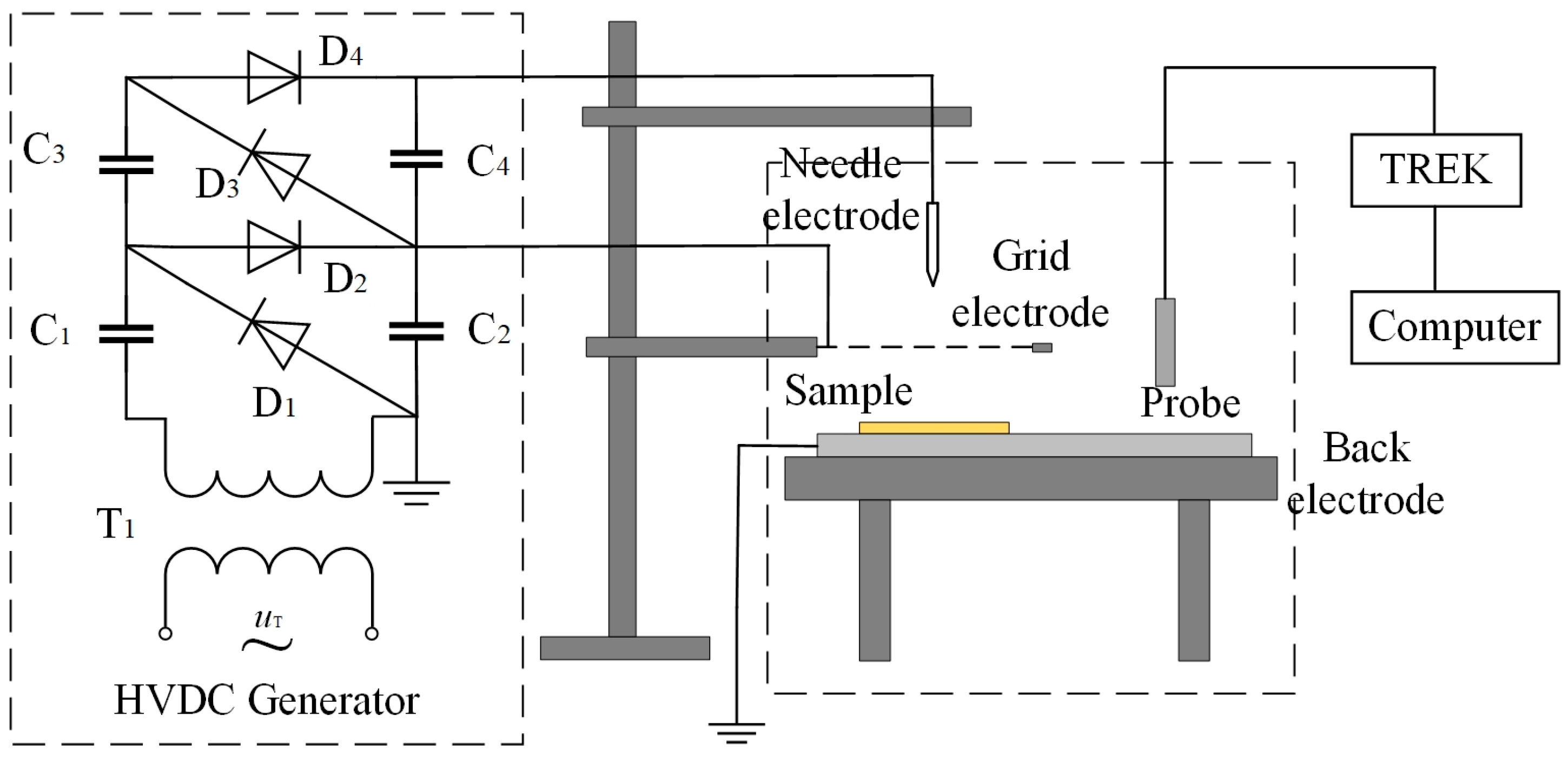
2. Mathematical Model

Surface charge migration characteristics are closely related to the charge transport characteristics within polymer materials. Many studies have shown that defects in polymer materials can form a large number of traps in the dielectric, which affect the charge migration by trapping and releasing carriers. The bipolar charge transport model is widely used to simulate the dynamic characteristics of the space charge in polymer materials, considering the injection, extraction, trapping, detrapping, and recombination of holes and electrons [24,25].
The charge transport can be described by the following set of equations [26,27]:
𝜕 n a ( x , t ) 𝜕 t + j a ( x , t ) = s a ( x , t )
j a ( x , t ) = μ a n a ( x , t ) E ( x , t ) D a n a ( x , t )
E ( x , t ) = ρ ( x , t ) ε 0 ε r
where the ‘a’ represents each kind of species, i.e., hm for mobile holes, em for mobile electrons, ht for trapped holes, and et for trapped electrons. n and j are the carrier density and current density, respectively, μ is the charge mobility, D = μ(kT/q) is the diffusion coefficient, k represents the Boltzmann’s constant, T denotes the temperature, q is the elementary charge, E represents the electric field, ρ is the net charge density, εr is the relative dielectric permittivity, and ε0 is the vacuum permittivity. s is the source term, indicating the change in the local charge density:
s h m = B h n h m ( 1 n h t / n 0 h t ) + D h n h t S 2 n e t n h m S 3 n e m n h m
s e m = B e n e m ( 1 n e t / n 0 e t ) + D e n e t S 1 n e m n h t S 3 n e m n h m
s h t = B h n h m ( 1 n h t / n 0 h t ) D h n h t S 0 n e t n h t S 1 n e m n h t
s e t = B e n e m ( 1 n e t / n 0 e t ) D e n e t S 0 n e t n h t S 2 n e t n h m
where Si is the recombination coefficients, Be and Bh are the trapping coefficients for electrons and holes, De and Dh are the detrapping coefficients for electrons and holes, and n0et and n0ht are the trap densities for electrons and holes.
A one-dimensional coordinate along the x direction was set up by our research group to investigate the charge carrier transport in the two-layered insulating medium, as is shown in Figure 1. x = 0 corresponds to the interface between the grounded conductor and insulation, while x = L, with L = L1 + L2, corresponds to the interface between the air and insulation.
The model assumes that the material layer is homogeneous, that is, the electrical parameters in the EPDM and PE layers are uniformly distributed in space, and the two-layered interface is an ideal flat interface, without considering interfacial defects and property gradients. This simplification aims to eliminate the interference of material microstructure differences and focus on the effects of charge injection and trap effects on the surface charge migration of the two-layered polymer film.
Due to the effect of corona discharge, the charge will deposit on the surface of the insulating medium to form a charge reservoir. The current density injected from the surface of the polymer film into the interior can be described by the detrapping probability of the trapped charge on the surface:
j 2 ( L , t ) = Q s ( t ) v A T E exp ( w s t k B T )
where j2(L,t) represents the injected current density, Qs(t) is the surface charge density, vATE is the attempt to escape frequency, and wst is the injection barrier of the corona-charged surface. Meanwhile, the charge injection at the ground electrode can be described by the Schottky formula:
j 1 ( 0 , t ) = A T 2 exp ( w i n k B T ) exp ( e k B T q E ( 0 , t ) 4 π ε 0 ε r )
where j1(0,t) denotes the current density by Schottky injection, A is Richardson’s constant, and win is the injection barrier between insulating medium and ground electrode.
The relevant parameters in the simulation referring to the works of other researchers and that gave the best fit are listed in Table 1 [4,24,28,29,30].

3. Results and Discussion
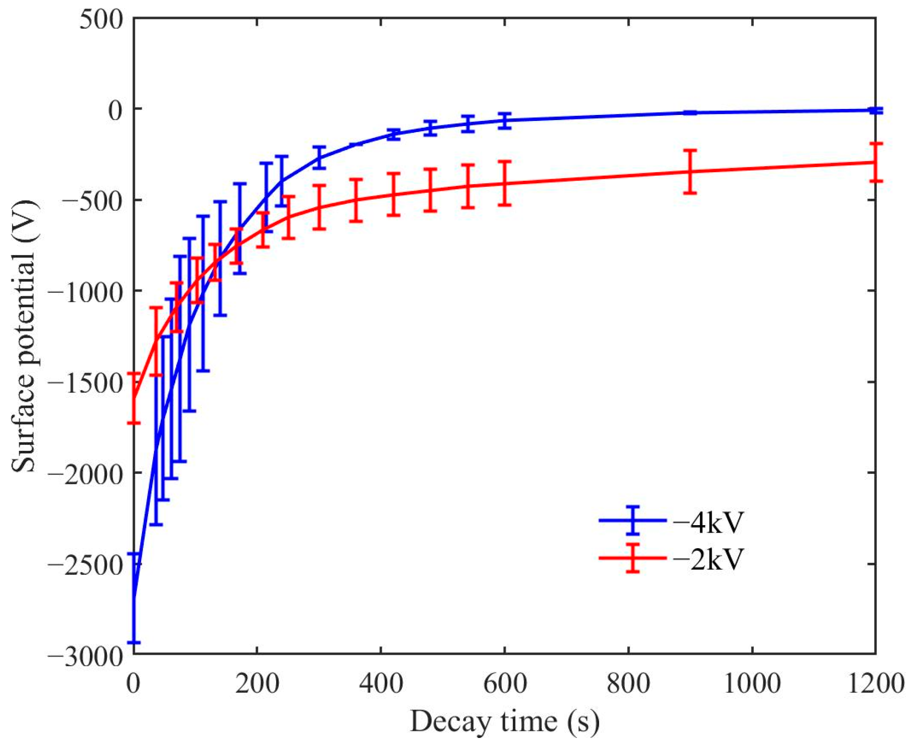
3.1. Benchmark

To validate the feasibility of the simulation model, SPD experiments were conducted on the EPDM/PE two-layered polymer film under −2 kV and −4 kV corona voltages. The PE films with a thickness of 0.5 mm used in the experiment were supplied by Shandong Lingxiang New Materials Co., Ltd., Weifang, China, and the EPDM films with a thickness of 1 mm were provided by Hebei Hongxiang Insulation Co., Ltd, Zhangjiakou, China. The samples were cut to a size of 25 mm × 25 mm, wiped clean with anhydrous ethanol, and then dried in a drying oven for more than 8 h. The treated samples were placed in a sealed bag and stored in a dry and dark environment for later use. The SPD experimental system, which mainly includes an HVDC generator, a needle-plate-grid electrode, a Trek-347 electrostatic potentiometer made by Lockport, NY, USA, and a computer, is shown in Figure 2. Among them, a four-stage series circuit is adopted in the power source, and a 220 V/2000 V single-phase step-up transformer is applied to the HVDC generator, with a maximum output voltage of 8 kV. The needle electrode and grid electrode are supplied by the HVDC generator. After charging the sample for 5 min, the sample is quickly moved to the position directly below the probe, and the potential values are measured and recorded. To ensure that the temperature and humidity do not affect the test results, the experiment was maintained at an ambient temperature of 25 °C and a constant relative humidity. The measured results were then compared with the simulation results.
Figure 3 shows the error bars for the simulated and measured results of the SPD for the EPDM/PE two-layered polymer film. The two curves in the figure are the average curves of the experimental and simulation results at −2 kV and −4 kV, respectively, and the error bars are used to represent the discreteness of the data. The error bars for both the simulated and measured curves are small and show good overlap, indicating that the simulation model is highly accurate.

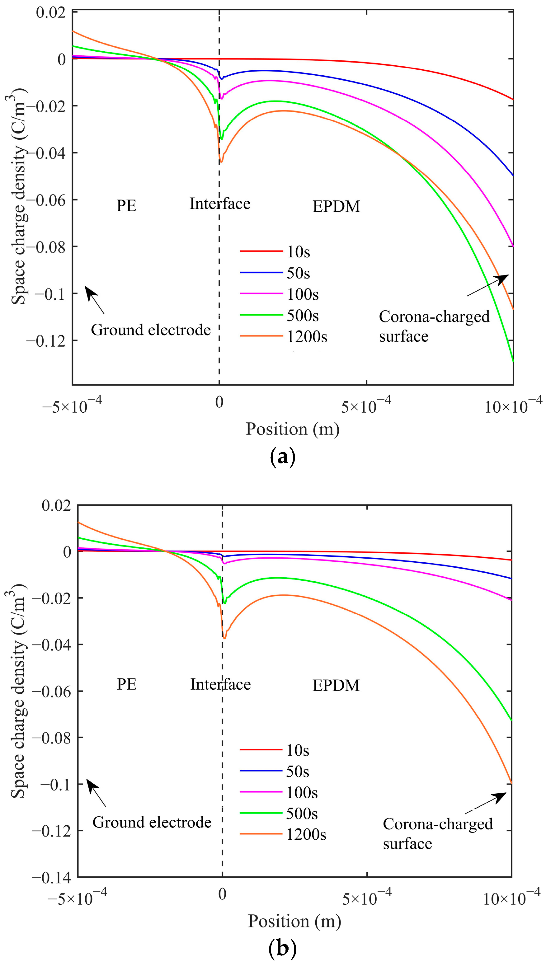
3.2. Effect of Injection on SPD Characteristics

When the EPDM material is doped with carbon black nanoparticles, a large number of deep traps are formed within the material; a cross section of carbon-black-doped EPDM composite is shown in Reference [31]. These deep traps can capture electrons injected by the electrode, thereby hindering electron migration within the material and increasing the difficulty of electron injection [30]. Additionally, the electrons trapped in the deep traps create a localized charge layer, which weakens the electric field near the electrode. The reduction in the electric field further limits the charge injection, leading to an increase in the injection barrier and consequently affecting the distribution and accumulation of space charge.
In this section, the effect of the injection barrier on the surface charge migration characteristics of the double-layer insulating dielectric surface is investigated based on nanoparticle doping. The value range of the injection barrier is relatively narrow [29,32]. Therefore, the injection barriers for EPDM are set to 0.93 eV, 0.95 eV, and 0.97 eV, and the SPDs of EPDM/PE under a negative corona voltage are obtained, as shown in Figure 4. The decay process is faster in the initial stage of SPD, after which the potential decreases more slowly. The difference in the decay rates between these two stages is primarily due to the varying trap energy levels of the surface charges on the sample. As the electron injection barrier decreases, the electron current density injected into the polymer film from the surface increases, leading to rapid surface charge dissipation.
Figure 5a and Figure 5b show the space charge density distributions for injection barriers of 0.93 eV and 0.97 eV, respectively, under a negative corona voltage. Holes and electrons are accumulated near the ground electrode and the corona-charged surface, respectively. The position x = 0 marks the interface. After the charging process is completed, surface charges continue to be injected into the film, leading to a gradual increase in the space charge density at the charged surface over time. Once the pre-deposited charges are fully dissipated, the space charge density at that location begins to decrease after 1200 s due to the influence of the charge transport mechanism within the dielectric, as shown in Figure 5a.
In Reference [29], the injection model of the LDPE monolayer medium has no interface effect, and the charge is mainly dissipated through the internal traps. However, during the SPD of the EPDM/PE two-layered medium, due to the mismatch in conductivity and relative permittivity at the insulating interface, only a portion of the charges can migrate into the adjacent dielectric through the interface, while the remaining charges accumulate as a negative space charge near the interface. The space charge density at the interface gradually increases from zero over time, reaching −0.044 C/m3 and −0.036 C/m3, respectively, after 1200 s. When the injection barrier increases, the dissipation rate of the surface charge slows down. This is because the higher injection barrier hinders the injection of the homopolar negative charge from the surface into the polymer film, making the surface charge decay mainly dependent on the release of charges in surface traps. At the same time, the interfacial charge accumulation is suppressed, which is due to the decrease in the amount of charges injected near the interface and the change in the distribution of electric fields at the interface. Furthermore, the electron detrapping probabilities at the dielectric surfaces with injection barriers of 0.93 eV and 0.97 eV are 1.14 × 10⁻³ s−1 and 2.40 × 10⁻⁴ s−1, respectively. As the injection barrier increases, the electron detrapping probability decreases significantly. Consequently, the electron density at the corona-charged surface is much higher under a 0.93 eV injection barrier than under a 0.97 eV barrier at the same time. This indicates that the change in the injection barrier has a significant effect on the SPD process, and the migration and accumulation of the surface charge can be effectively controlled by adjusting the injection barrier.

3.3. Effect of Trap on SPD Characteristics

During corona charging, the charges deposited on the surface of the two-layered insulating dielectric are primarily captured by surface traps. After charging, these surface-trapped charges are injected into the dielectric. During migration, the charges may become trapped by the traps. These trapped charges can be detrapped and can re-participate in the migration process when stimulated by external factors. The detrapped charges may be trapped again and migrate into the adjacent dielectric, until they are eventually extracted by the opposite electrode [33]. Traps play a crucial role in regulating the dissipation of the surface charge by influencing both charge migration and distribution.

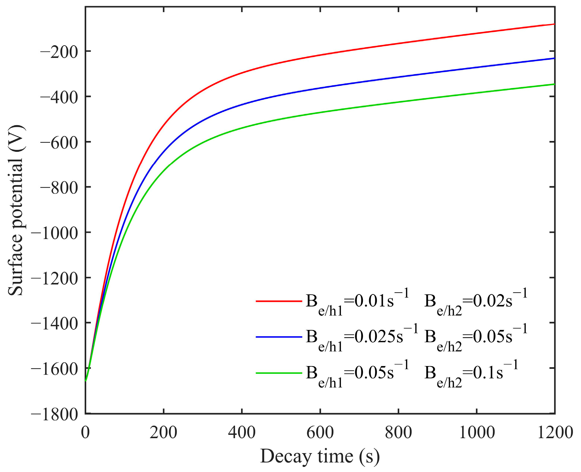
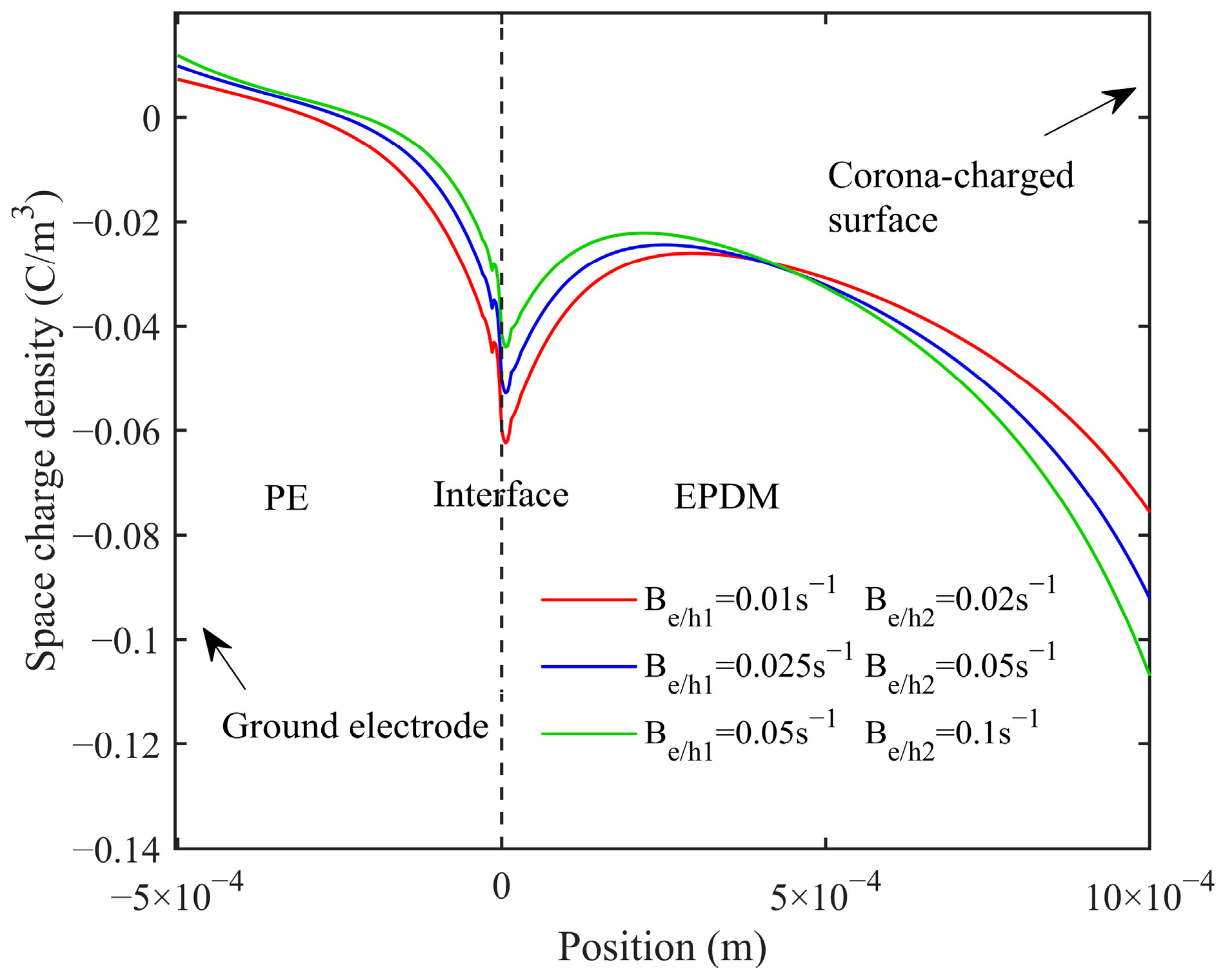
3.3.1. Trapping Coefficient
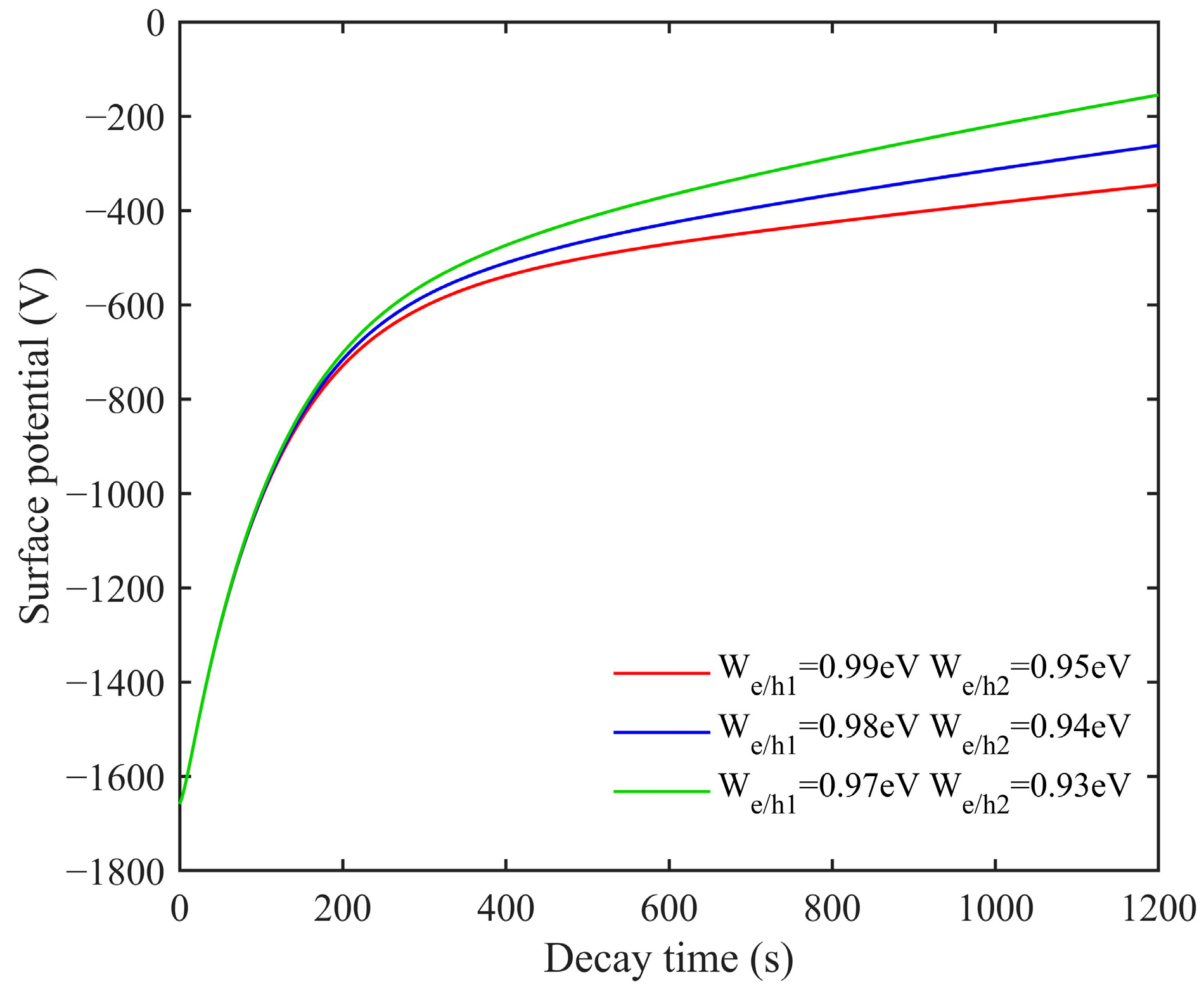
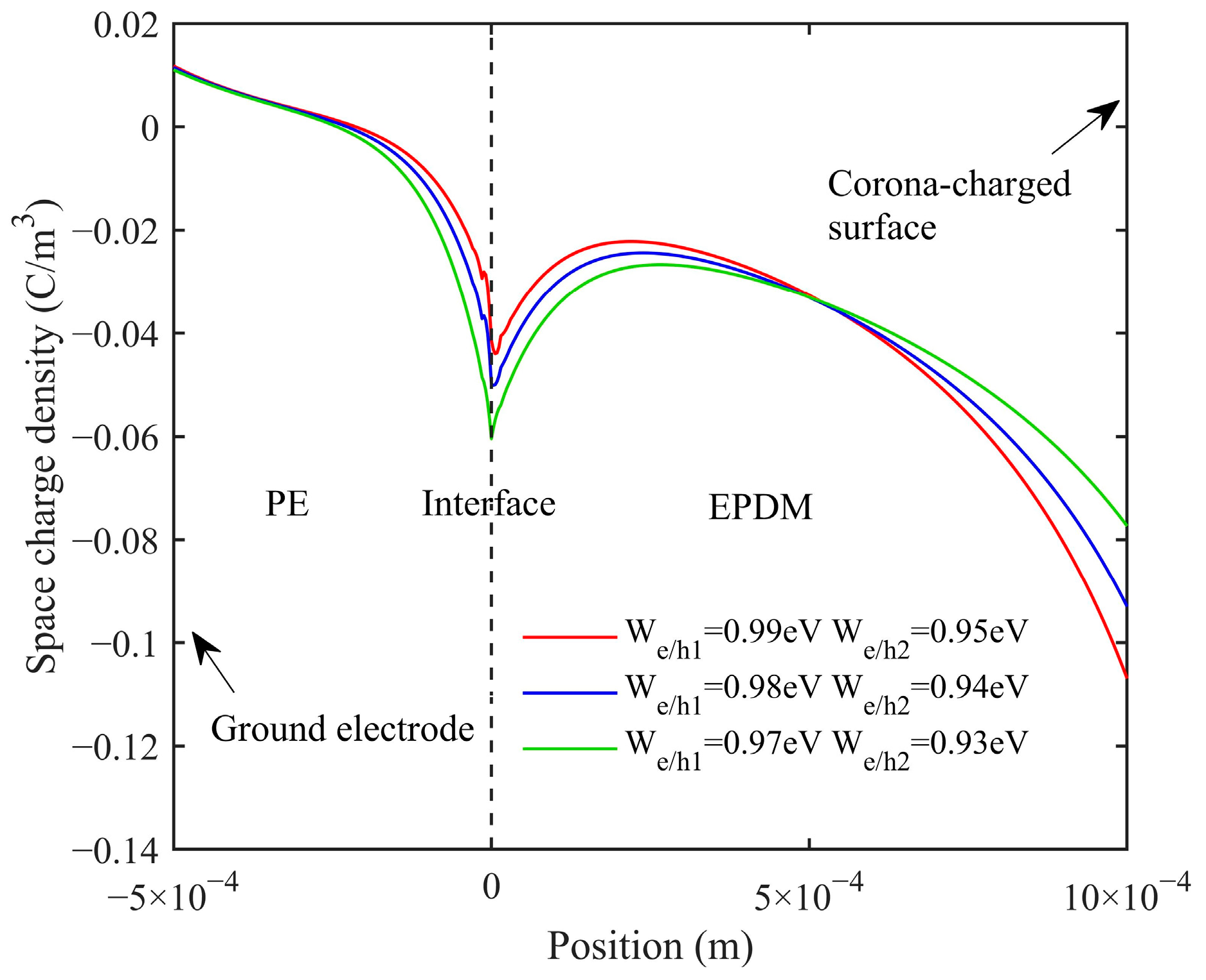
The local defects in EPDM and PE, particularly the disordered arrangement of molecular chains or the breakage of chemical bonds at the interface, generally affect the trapping coefficient of the material [34]. The disordered arrangement of molecular chains can increase carrier scattering, reducing mobility and providing more sites for carrier capture. Meanwhile, the breakage of interfacial chemical bonds can introduce dangling bonds or trap states, which have large capture cross sections, thereby increasing the trapping coefficient and space charge accumulation. It should be noted that this study concentrates on the relationship between the injection barrier and local defects. For the simplification of theoretical modeling, complex physical processes such as dipole relaxation and interfacial charge diffusion are not considered.
Local defects significantly influence the surface charge migration characteristics of carriers by altering the trapping coefficient. In this section, based on the basic parameters, the trapping coefficients are adjusted. The trapping coefficients for mobile electrons/holes in PE and EPDM are set as follows: Be/h1 = 0.01 s−1 and Be/h2 = 0.02 s−1, Be/h1 = 0.025 s−1 and Be/h2 = 0.05 s−1, and Be/h1 = 0.05 s−1 and Be/h2 = 0.1 s−1 [35,36]. Figure 6 shows the SPD of EPDM/PE polymer film under a negative corona voltage for different trapping coefficients. A decrease in the trapping coefficients reduces the ability of trap centers to capture electrons, allowing more electrons to move freely and participate in the transport process. This accelerates the dissipation of surface charges, ultimately leading to a lower stable surface potential.
Figure 7 demonstrates the simulated space charge density distributions with different trapping coefficients after 1200 s. In the two-layered polymer film, the space charge near the insulating interface is primarily formed by charges injected from the electrodes and migrating towards the interface, with the negative polarity charge injected by the corona voltage being dominant. After 1200 s, the space charge densities at the interface for Be/h1 = 0.025 s−1 and Be/h1 = 0.01 s−1 are −0.052 C/m3 and −0.062 C/m3, respectively. When the trapping coefficient is low, the charges stored in the insulating dielectric become unstable, and most of the trapped charges are detrapped and migrate both from the surface and within the dielectric over a short period. This process results in a decrease in the space charge density at the corona-charged surface, which corresponds to the SPD. Meanwhile, the low probability of carriers being trapped during migration results in a large number of carriers migrating towards and accumulating at the two-layered dielectric interface.
At the ground electrode, the hole injection follows the Schottky law, and the trapping coefficient affects the transport and accumulation of holes within the polymer film. During depolarization, positive charges accumulate near the ground electrode and migrate toward the opposite electrode under the influence of the electric field. As the trapping coefficient increases, more injected holes are captured by traps and accumulate near the electrode. Since the current density from the Schottky emission is much lower than that from the corona-charged surface, the injected holes are neutralized by electrons emitted from the opposite electrode before reaching the interface within the testing period.

3.3.2. Trap Depth

The overheating of EPDM and PE insulation materials during service can lead to thermal aging. This process triggers thermal oxidation reactions within the material, accelerating the degradation of the internal structure and the breakage of molecular chains, which generates more defects and mobile radicals. These defects may become trapping sites for electrons or holes, increasing the trap depths for both electrons and holes [37,38].
This scheme is based on simulating the changes in the depth of electron and hole traps in EPDM and PE materials during the thermal aging process. The range of trap depths is relatively narrow, typically between 0.85 eV and 1.05 eV [35]. Without considering temperature effects, the electron and hole trap depths for PE and EPDM are set as 0.99 eV and 0.95 eV, 0.98 eV and 0.94 eV, and 0.97 eV and 0.93 eV, respectively, to simulate the SPD of corona-charged EPDM/PE, as is shown in Figure 8.
The detrapping coefficients for EPDM at 0.95 eV and 0.94 eV are 5.23 × 10⁻4 s⁻1 and 7.72 × 10⁻4 s⁻1, respectively. As the trap depth decreases, the detrapping coefficient increases significantly, leading to a shorter residence time for charges in the traps. Accordingly, the potential decay rate at 0.93 eV is 11.56% higher than that at 0.95 eV within 1200 s. However, the SPD rates for different trap depths show noticeable overlap during the first 200 s of depolarization. This can be explained by the fact that a higher potential difference is formed between the sample surface and the ground electrode in the initial stage, and the charge migration is primarily driven by the external electric field, with a relatively minor influence of trap depth at this stage.
The amorphous regions in PE and EPDM contain polymer short chains, broken chains, long chains, and cross-linking points, which form traps of varying depths. These traps can capture and release charge carriers, thereby affecting the formation and accumulation of space charges in the dielectric. As the trap depth increases, the probability of charge carriers being trapped in the sample also increases. This makes it more difficult for injected electrons to migrate within the insulating layer, reducing the subsequent emission current density from the electrodes and the mobility of charge carriers near the charged surface, leading to the accumulation of a large amount of space charge near the surface. Moreover, the increased probability of trapping inevitably reduces the number of migrating mobile electrons and holes, resulting in less charge accumulation at the interface of the two-layered polymer film, with a difference of nearly 0.016 C/m3, as shown in Figure 9.
Compared to existing studies that primarily focus on single-layer polymers, our work advances the understanding of surface charge migration in two-layered structures. Reference [38] analyzed the trap distribution in a single-layered medium after thermal aging, and the results showed that thermal aging deepens the traps in the medium, which aligns with the findings of this study. In single-layered materials, charges are directly involved in the transport process in the medium once they are detrapped, with no interfacial barrier effect to hinder their movement. However, in the EPDM/PE two-layered structure, an increase in the trap depth significantly suppresses the interfacial charge accumulation. This indicates that, unlike in single-layered materials, the variation in trap depth in two-layered structures not only affects the migration of charges in the medium but also plays a crucial role in the interfacial charge accumulation.

4. Conclusions

The bipolar charge transport model is developed to study the SPD characteristics after the pre-deposited surface charge on an EPDM/PE two-layered polymer film, with thicknesses of 1 mm and 0.5 mm for EPDM and PE, respectively. The effects of nano-doping, local defects, and thermal aging on the surface charge migration characteristics of the EPDM/PE film are further discussed. The following conclusions are drawn:
(1) After the EPDM material is doped with nanoparticles, the electron injection barrier increases. This increase in the injection barrier slows down the dissipation of the surface charge and inhibits charge accumulation at the interface. After charging, the charge density at the surface gradually increases. Once the pre-deposited charge has completely dissipated, the charge density begins to decrease. Nano-doping can inhibit the charge accumulation at the interface by regulating the electron injection barrier, which provides a design basis for the optimization of insulation materials for HVDC cable accessories.
(2) The local defects in EPDM and PE can increase the trapping coefficient. The increase in the trapping coefficient suppresses the dissipation of surface charges, resulting in a higher stable surface potential. A higher trapping coefficient also leads to increased space charge density at the corona-charged surface and decreased charge accumulation at the interface. The holes injected by the anode are neutralized by electrons emitted from the counter electrode before reaching the interface. The influence of local defects on the trap coefficient can guide the defect engineering control of the insulation structure and improve the surface potential stability of the composite medium.
(3) Thermal aging increases the trap depth of electrons and holes in EPDM and PE insulation materials. This increase in trap depth significantly reduces the detrapping coefficient, inhibiting the dissipation of the surface charge in the two-layered polymer and reducing charge accumulation at the interface. During the early depolarization stage, the SPD rates at different trap depths are relatively similar, with charge migration primarily governed by the external electric field and less influenced by the trap depth. The change mechanism of trap depth caused by thermal aging provides theoretical support for insulation life prediction and reliability evaluation in high-temperature service environments and helps to solve the problem of aging failure in the long-term operation of high-voltage equipment.

Author Contributions

Conceptualization, X.C. and Y.L.; methodology, Y.L.; software, Y.L.; formal analysis, Y.L.; investigation, Y.L.; resources, X.C.; writing—original draft preparation, Y.L.; writing—review and editing, Y.L.; supervision, X.C.; project administration, X.C.; funding acquisition, X.C. All authors have read and agreed to the published version of the manuscript.

Funding

This research was funded by Natural Science Foundation of Liaoning Province, grant number 2020-MS-214 and Program for Innovative Talents in University of Liaoning Province, grant number LR2019047.

Data Availability Statement

The data used to support the findings of this study are available from the corresponding author upon request.

Conflicts of Interest

The authors declare no conflicts of interest.

References

  1. Li, Z.; Du, B. Polymeric insulation for HVDC extruded cables: Challenges and development directions. IEEE Electr. Insul. Mag. 2018, 34, 30–43. [Google Scholar] [CrossRef]
  2. Liu, Y.; Cai, X.; Cai, S. Study on space charge accumulation characteristics of 320 kV cross-linked polyethylene cable joints. Polym. Sci. Ser. A 2022, 64, 415–423. [Google Scholar] [CrossRef]
  3. Wang, Y.; Shuai, S.; Sun, Y.; Yang, X.; Liu, C. Effect of nano-MgO doping in XLPE on charge transport and electric field distribution in composite insulation of HVDC cable joint. Energies 2022, 15, 6948. [Google Scholar] [CrossRef]
  4. Wang, Y.; Wang, Y.; Yang, X.; Ma, A.; Sun, Y.; Yin, Y. Charge transport in full-size HVDC cable joint with modeling of XLPE/EPDM interface. IEEE Trans. Dielectr. Electr. Insul. 2021, 28, 2117–2125. [Google Scholar] [CrossRef]
  5. Han, Y.; Li, S.; Min, D. Trap energy distribution in polymeric insulating materials through surface potential decay method. IEEE Trans. Dielectr. Electr. Insul. 2018, 25, 639–648. [Google Scholar] [CrossRef]
  6. Du, B.; Li, X.; Jiang, J. Surface charge accumulation and decay on direct-fluorinated oil-impregnated paper. IEEE Trans. Dielectr. Electr. Insul. 2016, 23, 3094–3101. [Google Scholar] [CrossRef]
  7. Du, B.; Li, Z.; Li, J. Effects of direct fluorination on space charge accumulation in HTV silicone rubber. IEEE Trans. Dielectr. Electr. Insul. 2016, 23, 2353–2360. [Google Scholar] [CrossRef]
  8. Du, B.; Li, J.; Du, W. Surface charge accumulation and decay on direct fluorinated polyimide/Al2O3 nanocomposites. IEEE Trans. Dielectr. Electr. Insul. 2013, 20, 1764–1771. [Google Scholar] [CrossRef]
  9. Li, G.; Gu, Z.; Xing, Z.; Zhang, C.; Guo, S.; Hao, C.; Lei, Q. Space charge and trap distributions and charge dynamic migration characteristics in polypropylene under strong electric field. ECS J. Solid State Sci. Technol. 2022, 11, 083003. [Google Scholar] [CrossRef]
  10. Min, D.; Cho, M.; Khan, A.; Li, S. Surface and volume charge transport properties of polyimide revealed by surface potential decay with genetic algorithm. IEEE Trans. Dielectr. Electr. Insul. 2012, 19, 600–608. [Google Scholar] [CrossRef]
  11. Li, Z.; Yang, Z.; Du, B. Surface charge transport characteristics of ZnO/silicone rubber composites under impulse superimposed on DC voltage. IEEE Access 2018, 7, 3008–3017. [Google Scholar] [CrossRef]
  12. Wang, Y.; Wang, Y.; Yang, X. Interfacial charge dynamics of XLPE/EPDM double layers by simultaneous measurement of space charge and relaxation current. IEEE Trans. Dielectr. Electr. Insul. 2021, 28, 569–577. [Google Scholar] [CrossRef]
  13. Qi, B.; Yang, Z.; Yang, X.; Luo, Y.; Huang, M.; Gao, C.; Zhang, Y.; Li, C. A simplified method to estimate surface trap distribution: Potential decay by charge dissipation along surface. IEEE Trans. Dielectr. Electr. Insul. 2023, 30, 928–935. [Google Scholar] [CrossRef]
  14. Wang, F.; Wang, L.; Chen, S.; Zhong, L.; Sun, Q. Charge carriers on insulating surfaces: An experimental study. IEEE Trans. Dielectr. Electr. Insul. 2023, 30, 2665–2672. [Google Scholar] [CrossRef]
  15. Gödrich, S.; Schmidt, H.; Papastavrou, G. Stability of charge distributions in electret films on the nm-scale. ACS Appl. Mater. Interf. 2022, 14, 4500–4509. [Google Scholar] [CrossRef] [PubMed]
  16. Rabiee, S.; Sohrabi, M.; Afarideh, H. Electrostatic surface potential stability of corona charged PTFE electret films by some parametric optimization for radiation protection dosimetry. J. Electrostat. 2025, 133, 104013. [Google Scholar] [CrossRef]
  17. Huang, M.; Zhou, Y.; Chen, W.; Lu, L.; Jin, F.; Huang, J. Space charge dynamics at the physical interface in oil-paper insulation under DC voltage. IEEE Trans. Dielectr. Electr. Insul. 2015, 22, 1739–1746. [Google Scholar] [CrossRef]
  18. Qin, Y.; Ge, Y.; Zhao, J.; He, Y.; Lv, Z.; Wu, K.; Zhao, Y.; Zhou, Y. Characteristics of charge accumulation at the interface of double-Layer XLPE under DC voltage. IEEE Trans. Dielectr. Electr. Insul. 2025, 32, 707–716. [Google Scholar] [CrossRef]
  19. Das, S.; Gupta, N. Effect of ageing on space charge distribution in homogeneous and composite dielectrics. IEEE Trans. Dielectr. Electr. Insul. 2015, 22, 541–547. [Google Scholar] [CrossRef]
  20. Perrin, C.; Griseri, V.; Laurent, C. Measurement of internal charge distribution in dielectrics using the pulsed electro-acoustic method in non contact mode. IEEE Trans. Dielectr. Electr. Insul. 2008, 15, 958–964. [Google Scholar] [CrossRef]
  21. Rychkov, D.; Gerhard, R. Stabilization of positive charge on polytetrafluoroethylene electret films treated with titanium-tetrachloride vapor. Appl. Phys. Lett. 2011, 98, 139–312. [Google Scholar] [CrossRef]
  22. Chen, G.; Xu, Z.; Zhang, L. Measurement of the surface potential decay of corona-charged polymer films using the pulsed electroacoustic method. Meas. Sci. Technol. 2007, 18, 1453–1458. [Google Scholar] [CrossRef]
  23. Zhang, L.; Xu, Z.; Chen, G. Decay of electric charge on corona charged polyethylene. J. Phys. D Appl. Phys. 2007, 40, 7085–7089. [Google Scholar] [CrossRef]
  24. Liu, Y.; Cai, X.; Cai, S. Analysis of influence factors on space charge accumulation characteristics of 320 kV XLPE cable. Polym. Sci. 2022, 64, 415–423. [Google Scholar]
  25. Lan, L.; Wu, J.; Yin, Y.; Zhong, Q. Investigation on heterocharge accumulation in crosslinked polyethylene: Experiment and simulation. Jpn. J. Appl. Phys. 2014, 53, 071702. [Google Scholar] [CrossRef]
  26. Cai, X.; Wang, X.; Pang, D.; Zou, X.; Lu, Z. Investigation of current density, recombination rate and space charge density in polyethylene thin films based on bipolar charge transport model. Mater. Res. Express 2019, 6, 096451. [Google Scholar] [CrossRef]
  27. Baudoin, F.; Roy, S.; Teyssedre, G.; Laurent, C. Bipolar charge transport model with trapping and recombination: An analysis of the current versus applied electric field characteristic in steady state conditions. J. Phys. D Appl. Phys. 2008, 41, 025306. [Google Scholar] [CrossRef]
  28. Roy, S.; Segur, P.; Teyssedre, G.; Laurent, C. Description of bipolar charge transport in polyethylene using a fluid model with a constant mobility: Model prediction. J. Phys. D Appl. Phys. 2004, 37, 298–305. [Google Scholar] [CrossRef]
  29. Min, D.; Li, S. Simulation on the influence of bipolar charge injection and trapping on surface potential decay of polyethylene. IEEE Trans. Dielectr. Electr. Insul. 2014, 21, 1627–1636. [Google Scholar] [CrossRef]
  30. Li, J.; Liang, H.; Du, B.; Song, P.; Kong, X.; Li, Z. Numerical simulation of interface charge behaviors between LDPE/EPDM for HVDC cable accessory insulation based on the bipolar charge transport model. High Vol. Eng. 2018, 44, 1443–1449. [Google Scholar]
  31. Li, J.; Du, B.; Xing, Y. Trap distribution and flashover characteristics of Carbon-Black-Filled EPDM in low temperature. IEEE Trans. Appl. Supercond. 2016, 26, 0610305. [Google Scholar] [CrossRef]
  32. Zhong, X.; Zheng, Y.; Dang, B.; Miao, X.; He, J. Polarity effect on space charge distributions in polymer under DC electric field. Proc. CSEE 2016, 36, 6693–6701. [Google Scholar]
  33. Li, J.; Gao, Y.; Song, Z.; Peng, J.; Xu, X. On the crosslinking temperature dependence of charge transport behavior in XLPE film deduced from surface potential decay measurements. J. Electrostat. 2021, 109, 103539. [Google Scholar] [CrossRef]
  34. Li, Y.; Gao, B.; Li, X.; Yang, Y.; Xu, P.; Wang, Z. Evolution of trapping parameters of multi-layer oil-paper insulating medium at different partial discharge stages. High Voltage Eng. 2021, 47, 260–268. [Google Scholar]
  35. Tian, F.; Hou, C. A trap regulated space charge suppression model for LDPE based nanocomposites by simulation and experiment. IEEE Trans. Dielectr. Electr. Insul. 2018, 25, 2169–2177. [Google Scholar] [CrossRef]
  36. Anh, H.; Serdyuk, Y.; Gubanski, S. Charge transport in LDPE nanocomposites Part II—Computational approach. Polymers 2016, 8, 103. [Google Scholar] [CrossRef]
  37. Liu, Y.; Liu, H.; Yu, L.; Gao, L. Effect of thermal stress on the space charge distribution of 160 kV HVDC cable insulation material. IEEE Trans. Dielectr. Electr. Insul. 2017, 24, 1355–1364. [Google Scholar] [CrossRef]
  38. Li, H.; Li, J.; Ma, Y.; Yan, Q. Effects of thermal aging on the crystal structures of the XLPE cable insulating material at different temperatures. Proc. CSEE 2017, 37, 6740–6748. [Google Scholar]
Figure 1. Cross section of the equivalent insulation layer. L1 and L2 are the thicknesses of medium 1 and medium 2, respectively.
Energies 18 02552 g001
Figure 2. Schematic diagram of ISPD experiment.
Energies 18 02552 g002
Figure 3. Error bars for the simulated and measured results of the SPD for the EPDM/PE two-layered polymer film.
Energies 18 02552 g003
Figure 4. Simulated SPD of corona-charged EPDM/PE two-layered polymer film with various injection barriers.
Energies 18 02552 g004
Figure 5. Space charge density distributions in corona-charged EPDM/PE two-layered polymer film at various decay times when the electron injection barrier is (a) 0.93 eV and (b) 0.97 eV.
Energies 18 02552 g005
Figure 6. Simulated SPD of corona-charged EPDM/PE two-layered polymer film with various trapping coefficients.
Energies 18 02552 g006
Figure 7. Space charge density distributions in corona-charged EPDM/PE two-layered polymer film with various trapping coefficients at 1200 s.
Energies 18 02552 g007
Figure 8. Simulated SPD of corona-charged EPDM/PE two-layered polymer film with various trap depths.
Energies 18 02552 g008
Figure 9. Space charge density distributions in corona-charged EPDM/PE two-layered polymer film with various trap depths at 1200 s.
Energies 18 02552 g009
Table 1. Parameters used in the simulation.
ParametersPEEPDMUnit
Injection barrier of corona-charged surface, wst/0.93 [29]eV
Injection barrier between polymer and grounded electrode, win1.3 [30]/eV
Trapping coefficient for electrons, Be0.05 [24]0.1 [30]s−1
Trapping coefficient for holes, Bh0.05 [24]0.1 [30]s−1
Trap depth for electrons, we0.99 [24]0.95 [30]eV
Trap depth for holes, wh0.99 [24]0.95 [30]eV
Trapped density for electrons, n0et100 [28]100 [30]C/m3
Trapped density for holes, n0ht100 [28]100 [30]C/m3
Mobility for electrons, μe7.5 × 10−14 [4]1.35 × 10⁻¹³ [4]m2·V−1·s−1
Mobility for holes, μh2.4 × 10−14 [4]1 × 10⁻¹³ [4]m2·V−1·s−1
Recombination coefficient, S0 S1 S26.4 × 10−22 [28]6.4 × 10⁻²² [28]m3·s−1
Recombination coefficient, S30 [28]0 [28]m3·s−1
Disclaimer/Publisher’s Note: The statements, opinions and data contained in all publications are solely those of the individual author(s) and contributor(s) and not of MDPI and/or the editor(s). MDPI and/or the editor(s) disclaim responsibility for any injury to people or property resulting from any ideas, methods, instructions or products referred to in the content.

