Review

Wide-Bandgap Subcells for All-Perovskite Tandem Solar Cells: Recent Advances, Challenges, and Future Perspectives

by
Qiman Li
1,
Wenming Chai
1,
Xin Luo
1,
Weidong Zhu
1,
Dazheng Chen
1,
Long Zhou
1,2,
He Xi
1,2,
Hang Dong
1,
Chunfu Zhang
1,* and
Yue Hao
1
1
State Key Laboratory of Wide-Bandgap Semiconductor Devices and Integrated Technology & Shaanxi Joint Key Laboratory of Graphene, School of Microelectronics, Xidian University, Xi’an 710071, China
2
School of Advanced Materials and Nanotechnology, Xidian University, Xi’an 710071, China
*
Author to whom correspondence should be addressed.
Energies 2025, 18(10), 2415; https://doi.org/10.3390/en18102415
Submission received: 31 March 2025 / Revised: 26 April 2025 / Accepted: 6 May 2025 / Published: 8 May 2025

Abstract

:
All-perovskite tandem solar cells (APTSCs) offer a promising pathway to surpassing the efficiency limits of single-junction photovoltaics. The wide-bandgap (WBG) subcell, serving as the top absorber, plays a critical role in optimizing light harvesting and charge extraction in tandem architectures. This review comprehensively summarizes recent advancements in WBG subcells, focusing on material design, defect passivation strategies, and interfacial engineering to address challenges such as phase instability, halide segregation, and voltage losses. Key innovations, including compositional tuning, additive engineering, and charge transport layer optimization, are critically analyzed for their contributions to efficiency and stability enhancement. Despite significant progress, challenges remain regarding scalability, long-term stability under illumination, and cost-effective fabrication. Future research directions include the development of lead-reduced perovskites, machine learning-guided material discovery, and scalable deposition techniques. This review provides insights into advancing WBG subcells toward high-efficiency, stable, and eco-friendly APTSCs for next-generation solar energy applications.

1. Introduction

Perovskite solar cells (PSCs) have engendered significant scholarly attention in photovoltaics due to their high absorption coefficient, tunable bandgap, and low-cost fabrication processes [1,2,3,4,5]. In the photovoltaic field, halide perovskite materials have been distinguished from other emerging semiconductor systems, such as 1D nanostructures [6,7] with peculiar optical and electronic properties and 2D superlattices [8] that enable the precise modulation of excitonic properties through compositional and structural modifications. Over the years, there has been considerable advancement in single-junction PSCs, and the certified power conversion efficiency (PCE) has risen from 3.8% to 27% [9,10]. To surpass the S-Q limit in single-junction solar cells, constructing tandem solar cells (TSCs) has emerged as the prevalent approach in recent research [11,12]. This strategy involves vertically stacking multiple cells in descending order of bandgap energies, where high-energy photons are preferentially absorbed by the wide-bandgap (WBG) top subcells, while transmitted lower-energy photons are harvested by subsequent narrow-bandgap (NBG) subcells [2,4,13]. This effectively improves the device’s efficiency by optimizing the absorption of the solar energy spectrum. Among several TSCs, all-perovskite tandem solar cells (APTSCs) employing perovskite subcells are distinguished in the photovoltaic field.
In addition, APTSCs can break through the single-junction S-Q limit and are prepared at a lower manufacturing cost due to the abundant raw materials compared to other TSCs [2,14,15]. The fabrication process is relatively simple, as most devices can be manufactured through solution methods under low-temperature conditions, thereby further reducing energy consumption [16,17]. Moreover, both subcells in APTSCs can precisely regulate the bandgap to achieve improved spectral matching and enhanced device lattice-matching capabilities, accompanied by a reduced interfacial defect [18,19,20]. Furthermore, APTSCs demonstrate significant application versatility due to their lightweight nature, enabling integration with flexible substrates [21,22,23]. APTSC structures are classified into two types based on whether the subcells are independent devices: two-terminal (2-T) structures and four-terminal (4-T) structures [17,24,25,26]. In APTSCs, the WBG top subcells constitute the important building block of tandem cells, making the photovoltaic performance of WBG PSCs a pivotal factor in efficient APTSCs [27,28]. Despite the substantial research efforts that have been made in recent years, WBG PSCs still face persistent challenges, including phase stability and energy losses [17,29,30]. Achieving high open-circuit voltages (Voc) approaching theoretical limits remains particularly challenging for WBG PSCs with bandgaps exceeding 1.7 eV [2,14,31,32]. In contrast to conventional PSCs, WBG PSCs characteristically manifest Voc deficits, which are attributed to photo-induced phase segregation, perovskite film grain boundary defects, and energy alignment mismatches [33,34,35]. Photovoltaic research has focused on advancing efficient and stable WBG PSCs, resulting in substantial progress in this field. Therefore, it is crucial to review the recent advancements in WBG PSCs, along with an in-depth discussion on the future research directions in the field of TSCs.
This review provides a comprehensive overview of the latest development in WBG subcells for APTSCs, focusing on compositional engineering and interface modification in WBG perovskite films to regulate crystallization growth and improve charge transportation. These strategies were employed to passivate non-radiative recombination defects, mitigate energy level misalignment, and improve charge extraction, thereby boosting photovoltaic performance in tandem devices. Meanwhile, critical challenges such as scalability, long-term stability, and flexible device applications are analyzed, and some suggestions are proposed. The potential of WBG perovskites in diverse applications is explored, emphasizing the necessity of interdisciplinary innovation to overcome existing limitations. In contrast to existing reviews on APTSCs, which either provide broad discussions encompassing both subcells or focus exclusively on NBG bottom subcell advancements, this review presents one of the few comprehensive analyses specifically dedicated to research progress in WBG top subcell development, which may provide new insights for researchers. This review summarizes the research progress of WBG top cells in APTSCs from two primary perspectives: compositional engineering and interface modification. Within compositional engineering, the discussion is organized into two distinct approaches: the substitution of A-site cations, B-site cations, and X-site anions in the perovskite lattice, and the incorporation of other additives. Regarding interface modification, the analysis is divided into two key strategies: upper interface treatment and bottom interface modification. The following table of contents outlines the structure of this review.

2. Composition Engineering

Compositional engineering of perovskite materials has been confirmed to regulate the bandgap through the adjustment of their internal components, thus providing a solid foundation for the preparation of APTSCs [36]. WBG perovskites with varying ionic compositions will manifest distinct crystal structures, thereby influencing the electronic structure of perovskite films [21,22,37,38]. In addition, the rapid crystallization growth inevitably results in a high defect density within the perovskite films during the annealing process through the solid-solution method [39], leading to further increased Voc losses and the deteriorated photostability of the perovskite devices [40]. It has been shown that regulating the ion components or adding additives in perovskite precursors can improve the crystallization of perovskite to greatly improve the photoelectronic properties and device stability of WBG PSCs [41]. Consequently, it is important to explore the effect of composition variations on the correlation between the device performance of the corresponding devices. For composition engineering, the types of additives in perovskite precursors are summarized, such as the addition of A-site cations, B-site cations, X-site anions, and other specific additives into the perovskite precursor to enhance the efficiency and stability of the WBG subcell in APTSCs.

2.1. A-Site Cations, B-Site Cations, and X-Site Anions

Within the perovskite structure, there are A-site cations, B-site cations, and X-site halide anions. The bandgap of the perovskite can be regulated through the manipulation of ion types and ratios at the three distinct locations [33]. As shown in Figure 1a, the A-site cation can substantially influence the bond length and angle of the B-site cation and X-site anion within the [BX6]4− octahedral structure, which is achieved by changing the shape and size of the A-site cation, thus resulting in modifications to the physical structure of the whole perovskite crystal [18,19]. Consequently, adjusting the A-site cation size enables bandgap tuning, thereby regulating the optical properties of the perovskite crystal. The B-site cation exhibits a significant influence on the bond angle in the [BX6]4− octahedron, with the potential to enhance the angle to reduce the bandgap. The halide ionic radius at the X-site demonstrates a substantial impact on the valence energy level, which is reduced by increasing the ionic radius to decrease the valence energy level. In addition, decreasing the valence energy level can be used to reduce the bandgap [22,42]. Furthermore, the crystallization of perovskite films and defect passivation can be influenced by adding new materials to the perovskite precursor. By adjusting the ion types and ratios at the A-, B-, and X-sites, as well as by incorporating new materials into the perovskite precursor, the crystal structure, octahedral bond angles, valence energy level, and defect passivation can be modulated, thereby regulating the bandgap and optical properties of the perovskite.
The A-site cation is considered to be one of the most significant components of the lattice structure, including formamidine (FA+), methylammonium (MA+), cesium (Cs+), rubidium (Rb+), and so on [33,40]. As an organic cation, MA+ plays an important role in the perovskite precursor to form stable complexes with anions such as iodide, thus suppressing the deprotonation of organic Cscations in solution and enhancing the precursor’s stability, thereby impacting perovskite crystallization and reducing the grain boundary’s density. As a result, it is employed to decrease non-radiative recombination and enhance the carrier’s lifetime [44]. Introducing FA+ into perovskite has been demonstrated to expedite ion coordination within the perovskite lattice during the crystallization process. This phenomenon has been shown to enhance the compositional homogeneity of initial small grains and perovskite crystallinity [45]. In Figure 1b, Eperon et al. [43] synthesized tunable lead trihalide perovskites with a bandgap of 1.48–1.73 eV. The A-site cations, which play a critical structural role in perovskites, exhibit distinct bandgap characteristics depending on their chemical composition. The UV–vis absorption spectra demonstrate significant variations when Cs, MA, and FA cations are employed as the A-site constituents in the perovskite structure. A single cation at the A site in perovskite precursors has a limited stabilizing effect in PSCs. As a result, introducing multiple cations at the A site can boost the grain size and reduce grain boundaries in perovskite films, hence lowering carrier recombination and improving PCE, further stabilizing the perovskite crystal’s structure. Although some alternative organic cations (such as MA+ and FA+) can enhance the device’s performance, these impurities might reduce the long-term stability of perovskite films. Philippe et al. [46] revealed that incorporating inorganic cations (such as Cs+ and Rb+) further improves structural stability in perovskite materials. As shown in Figure 2a–c, Cs+ has significant advantages in improving the crystallization quality and bandgap regulation of perovskite films, which helps in preparing perovskite solar cells with better performance. Analysis of Figure 2a reveals that any stoichiometric variation in A-site cations directly modifies the surface crystallization behavior of perovskite structures. Through a comparative examination of Figure 2b,c, it becomes evident that the incorporation of different A-site cations significantly influences the coordination chemistry within the perovskite matrix, particularly affecting the bonding characteristics of Pb-I and Pb-Br configurations. Zhang et al. [47] utilized a sophisticated quantum dynamics simulation technique to examine how Cs+ doping inhibits ion migration in low-dimensional perovskite structures. Their findings revealed that the incorporation of Cs+ could effectively impede ion migration, thereby enhancing the stability of the crystal structure. A subsequent detailed analysis of the crystallographic changes induced by Br/Cs doping provided further insights into the mechanism of Cs+ ion-mediated ion migration inhibition in MAPb(I1−xBrx)3. This offers significant advancements in our understanding of ion migration inhibition in perovskite materials, particularly regarding the Cs+ doping effects. As shown in Figure 2d, Prasanna et al. [48] incorporated Cs+ into the Pb-based perovskite, thereby enhancing the bandgap of the perovskite, mitigating phase segregation, and reducing the Voc deficit to achieve an efficiency of 17.8%. The variation in Cs concentration induces distinct Pb peaks in the XRD patterns, which demonstrates that different Cs content levels can directly influence the crystallization of perovskite materials, consequently affecting the bandgap variation. Xie et al. [49] investigated the potential aggregation problem of PbI2 and found that incorporating Cs+ into the perovskite precursor can enhance PbI2 solubility, thereby reducing its aggregation. In 2022, Guo et al. [20] compared the effects of CsBr and cesium formate (CsFa) in a perovskite precursor with a bandgap of 1.63 eV. They found that the CsFa additive increased the crystallinity, achieving a PCE of 20.1%. Meanwhile, an appropriate amount of Rb+ can regulate the growth of perovskite grains, increasing their size and forming dense films. Moreover, the addition of a low proportion of Rb+ can enhance carrier transport and extraction efficiency, improving the photovoltaic performance of PSCs. As shown in Figure 2e, Wang et al. [50] optimized a Rb+ additive in the precursor to improve the crystallization of perovskite films. An appropriate concentration of Rb⁺ ions effectively suppresses the emergence of impurity peaks in the XRD pattern. Furthermore, Duong et al. [51] found that rubidium thiocyanate (RbSCN) can slow crystal growth to improve the crystallinity of WBG perovskite films, inhibiting defect migration and enhancing photostability. In 2024, Sun et al. [52] added 20% CsI and 4% RbI in the precursor, which not only enhanced crystallization during perovskite formation but also removed PbI2 residues. As a result, the PCE of 1.7 eV WBG PSCs reached 20.6%. When both FA+ and MA+ are present, adding Cs+ to the precursor can achieve better results [53]. Makhsud et al. [54] found that hybrid CsMAFA perovskites have higher stability than single cationic perovskites due to their atomic vacancies, based on in-depth studies by other researchers. Zhao et al. [55] demonstrated that the PCE of PSCs increased with the increasing amount of Cs+ under fixed amounts of FA+ and MA+, enhancing crystallization and reducing defects due to the formation of FA-Cs. Son et al. [56] sought to circumvent the J–V hysteresis effect of PSCs by adding potassium iodide (KI) to the perovskite precursor, and the elimination of the hysteresis effect was nearly achieved. Subsequent deliberate experiments utilizing alkali metal iodides, including LiI, NaI, KI, RbI, and CsI, revealed that the presence of potassium ions resulted in a substantial reduction of the hysteresis effect, which indicates that the J–V hysteresis effect observed in PSCs can be attributed to Frenkel defects in iodides, where potassium ions serve to prevent the formation of these defects by providing energy to the interstitial sites. In summary, this study demonstrates that the developed KI doping method can be universally applied to achieve hysteresis-free perovskites, irrespective of the composition and device structure. In addition to these common ions, some other ions are doped into the perovskite precursor as A-site ions to enhance the performance of PSCs. Palmstrom et al. [57] enhanced the stability of the WBG perovskite film by utilizing dimethylamine (DMA) as an A-site cation for bandgap regulation. However, wide bandgap mixed halide perovskites based on FA+ and MA+ are susceptible to high-density traps and pinholes [58]. In 2024, Zhou et al. [59] used the large organic cation 2-(4-fluorophenyl) ethylammonium (F-PEA+) as the A-site cation to form a 2D/3D structure. This approach successfully suppressed the photo-induced halide phase separation in WBG perovskites (1.78 eV), thereby enhancing phase stability and optoelectronic properties. Consequently, the PCE of WBG PSCs reached 19.4%, leading to the APTSCs achieving a PCE of 27%. When combined with the NBG subcells, a new approach was proposed to enhance efficiency. To inhibit ion migration and photo-induced halide segregation, Tian et al. [60] recently developed new methylenediammonium cations (MDA2+) to partly replace the A-site cations in the perovskite lattice. In addition, they also carefully investigated the interaction between MDA2+ and other ions in perovskite precursors during crystallization, providing new A-site cation materials to improve the performance of 4-T APTSCs. This mixed engineering process of A-site cations has been demonstrated to result in either lattice expansion or contraction. This section exemplifies the functional roles of various A-site cations in compositional engineering. Beyond bandgap modulation, the appropriate incorporation of A-site cations enhances crystallization quality and suppresses defect formation. Mixed-cation combinations synergistically regulate perovskite growth while highlighting their respective advantages and limitations, offering novel insights for advancing perovskite solar cell research.
The B-site cations are primarily constituted of metal cations, including lead (Pb2+), tin (Sn2+), and copper (Cu2+), which contribute to the crystallinity and phase stability of perovskite [29]. Pb2+ is commonly found in the WBG subcell of APTSCs and is the most frequently used B-site cation. As the B-site cation in perovskite precursors, Pb2+ can form stable ionic bonds with halide anions, facilitating perovskite structure formation and stability. In addition, Pb2+-based perovskites demonstrate extended carrier diffusion lengths and high carrier mobility, enabling efficient charge transport in photovoltaic devices. In addition, Pb2+ also suppresses the transformation from perovskite to non-perovskite phases, thus enhancing the thermal and moisture stability of perovskite films. Zhou et al. [44] discovered that the incorporation of Pb(SCN)2 into the perovskite precursor facilitates the healing of grain boundaries in conjunction with the optimal proportion of FAX, thereby enhancing film crystallinity and increasing the grain size [61]. Sn2+ usually acts as the B-site cation in the NBG perovskite precursor and is mostly found in the bottom subcell of NBG in APTSCs, which is not the focus of this review, so there are no examples given here. Later, we will review Pb-free WBG perovskite, a kind of WBG perovskite precursor with Sn2+, which typically utilizes Sn instead of Pb to enhance environmental sustainability and can be used as the top cell of APTSCs. However, Pb-free WBG perovskite also exhibits numerous drawbacks, including its rapid crystallization rate, which can lead to the formation of various defects. Additionally, Sn can easily oxidate in ambient atmospheres, compromising its stability [62]. Specific improvement strategies will be summarized in the subsequent section on additives. In their investigation, Wang et al. [63] studied the properties of a CsPbI2Br perovskite. Copper-based perovskites are less studied, but they have clear advantages. Compared with some metal cations, Cu2+ has relatively low environmental toxicity. In addition, Cu2+ can participate in redox reactions using its rich valence states within the perovskite structure to increase the carrier concentration, thus modulating the electronic structure and conductivity of perovskites and ultimately improving the performance of PSC devices. They achieved an increase in crystal size by doping CuBr2 into the perovskite precursor, which increased the carrier’s mobility and reduced its trap state, thereby improving the quality of the perovskite film. The champion PSCs prepared demonstrated a PCE of 16.15%. In the future, researchers may explore more metal cations as B-site cations in perovskite precursors to enhance the efficiency and stability of WBG PSCs. B-site cations such as Pb2+, Sn2+, and Cu2+ exhibit distinct advantages and development potential across multiple research directions. Although limited alternatives for B-site cation substitution exist in WBG PSCs, novel breakthroughs still emerge in aspects such as industrialization and environmental protection, warranting further exploration.
Adjusting the X-site halogen anion, including iodine (I), bromine (Br), and chlorine (Cl), has been identified as a viable method for the synthesis of wider-bandgap perovskites. They also coordinate with metal ions such as lead, forming compounds such as PbI3 and PbI42⁻, which are essential for perovskite formation. Properly increasing the I concentration boosts crystallization, allowing for better grain growth and enhancing the crystal’s qualities. As shown in Figure 3a,b, Cao et al. [64] found that adjusting the amount of I in the presence of Br by varying the KI concentration in the perovskite precursor could achieve a bandgap redshift, enhancing the light absorption range and efficiency of PSCs. Finally, it is determined that incorporating 20% KI into the perovskite precursor maximizes the perovskite film’s grain uniformity. The introduction of Br can alter the bandgap of perovskites, thus affecting their light absorption. In addition, during the annealing process, the strong coordination between Br and Pb2+ stabilizes the perovskite structure and hinders phase transformation. In addition, Br can form intermediate phases with other components, obstructing the crystallization of perovskite precursors and reducing the nucleation rate, thereby regulating the perovskite crystal’s growth process. I and Br are often used together because the bandgap of perovskite can be tuned by the ratios of these two ions. Tanaka et al. [65] made a comparative study on the use of Br and I at the X site, which shows that the replacement of I with Br has been demonstrated to result in the formation of wider-bandgap perovskites. Noh et al. [66] used an incomplete substitution of Br with I to regulate the bandgap spanning almost the entire spectrum and increase phase stability. As depicted in Figure 3c, this process clearly demonstrates that when I and Br ions act as X-site anions, they form distinct perovskite structures with corresponding variations in bandgap energies. As a common method for bandgap regulation, Chiang et al. [67] adjusted the I/Br ratio in the perovskite precursor to compare the influence of different bandgaps on device efficiency. Finally, the researchers tuned the perovskite bandgap from 1.62 to 1.80 eV by changing the evaporation rate of PbBr2 during the preparation of the precursor. In comparison with MAPbI3, MAPbBr3 exhibits stronger Pb–Br bonds, a more compact arrangement of the cubic lattice, and enhanced phase stability [29]. However, the solubility of the bromide leads is too low to regulate crystallization and the formation of pores. Recently, Fang et al. [68] demonstrated that a lower Br concentration is advantageous for enhancing photostability, which effectively passivates grain boundaries and minimizes impurity formation within the perovskite films. The champion output efficiency is reported to reach 22.28%. Cl has strong coordination abilities with metal cations (such as Pb2+), enhancing the solubility of metal salts in perovskite precursor solutions. It also adjusts the colloidal properties of perovskite precursor solutions, reducing particle aggregation and sedimentation for more uniform crystallization in perovskite films. Additionally, Cl can act as a template to improve the direction of grain growth and increase perovskite grain size. Recently, Siegrist et al. [69] analyzed the effects of Cl on the perovskite’s crystal structure and the photostability of WBG (1.8 eV) subcells in APTSCs. As illustrated in Figure 3d, they prepared perovskite doped with ACl, PbCl2, and APbCl3 via blade coating to explore distinctions. It shows that 5% mol CsPbCl3 in p-i-n PSCs achieved a PCE of 17.5% at 0.062 cm2 and enhanced film uniformity for large-area (10 × 10 cm2) devices, offering new ideas for the industrialization of APTSCs. Doping Cl into hybrid CsMAFA-based perovskites further inhibits the generation of atomic vacancies. The incorporation of Cl into the hybrid CsMAFA perovskites has been shown to enhance the concentrating intensity of the films by factors of five and ten, respectively, thereby significantly improving the stability of the devices [19]. In addition, some other anions can be used as X-site ions in perovskite precursors, such as thiocyanate (SCN). The effective ionic radius of SCN is close to that of I, enabling it to bond with Pb2+ to develop a stable perovskite structure, thereby enhancing the humidity stability of perovskite films. Zhou et al. [44] discovered that the incorporation of Pb(SCN)2 into the perovskite precursor, in conjunction with the optimal proportion of FAX, facilitates the healing of grain boundaries, thereby enhancing the crystallinity and increasing the grain size [61]. Although researchers have extensively studied halide ions at the X site, their behavior during perovskite crystallization is still difficult to control precisely, leading to issues such as non-radiative recombination losses. Numerous X-site anions can coordinate with cations to modulate the perovskite bandgap or facilitate crystallization, analogous to the roles of A-site cations. The combination of multiple X-site anions in varying ratios yields distinct effects and functionalities. Despite the aforementioned challenges, research on X-site anions continues to provide novel insights for advancing perovskite optimization.
In compositional engineering, the A-site, B-site, and X-site ions constitute the perovskite structure. For WBG perovskites in APTSCs, the coexistence of three ionic components in perovskite precursors demonstrates remarkable effectiveness in both bandgap fine-tuning and crystallinity enhancement. For the same ions, varying concentrations of identical ionic species induce distinct crystallization behaviors, while mixed-ion configurations exhibit greater potential in regulating crystallization kinetics and defect suppression, thereby offering broader research prospects.

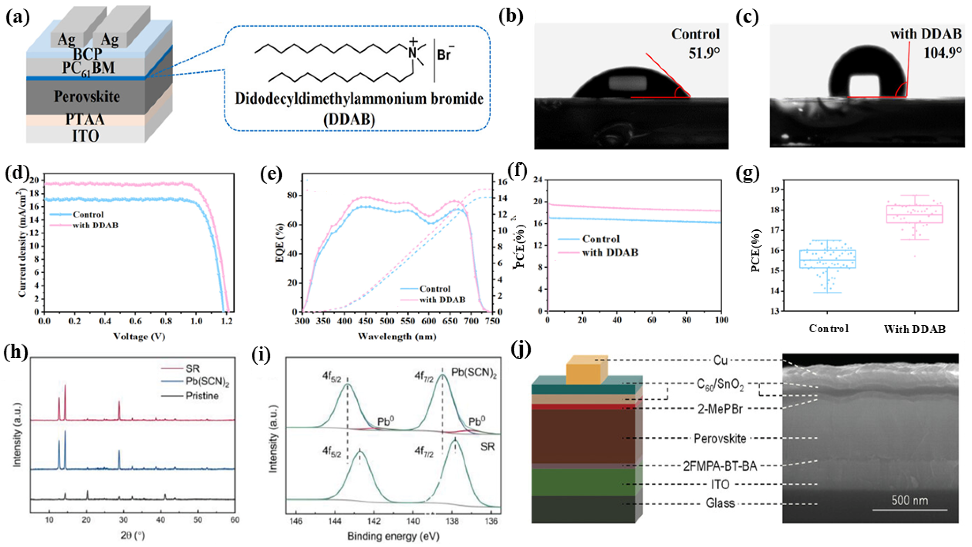
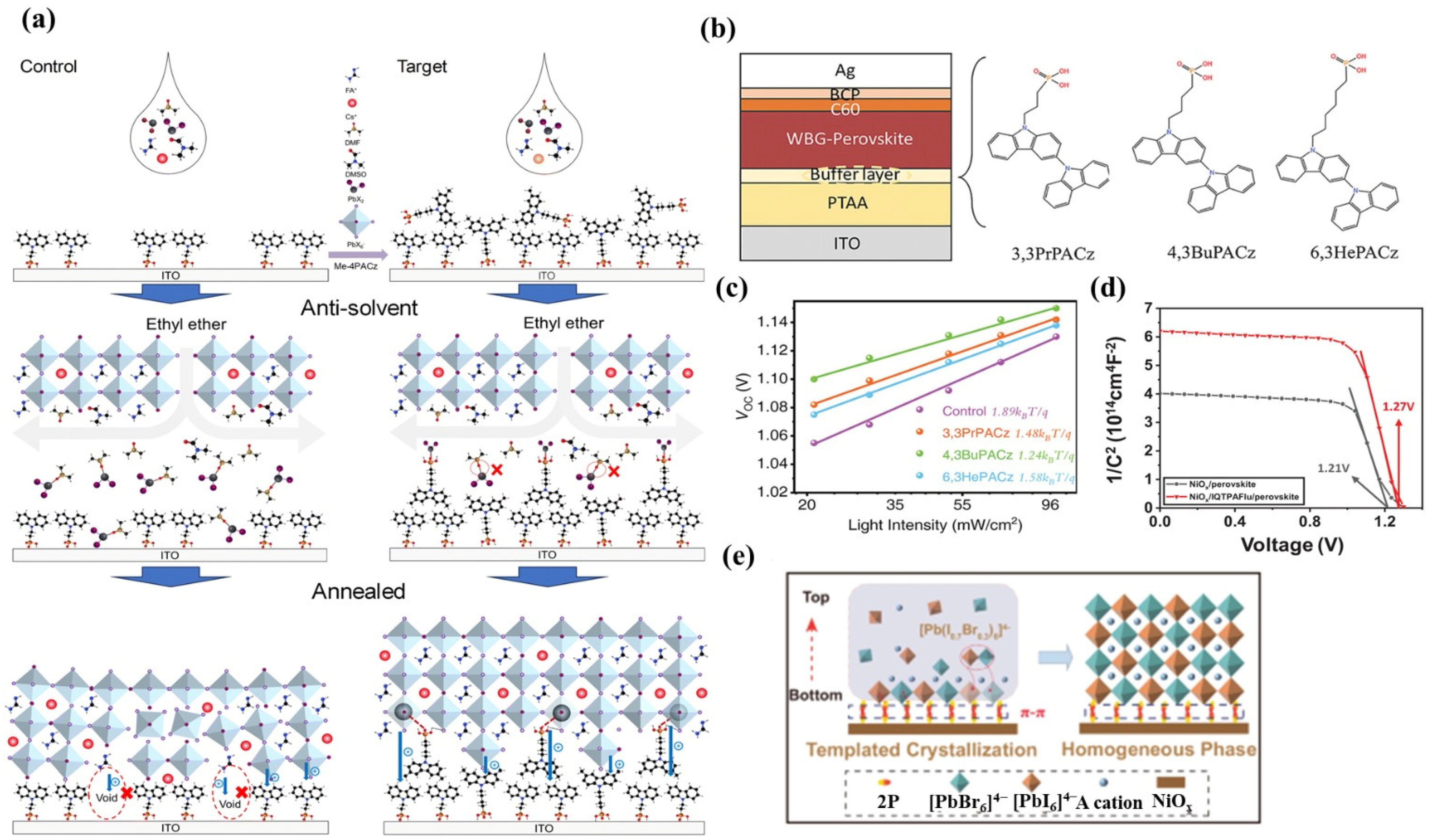
2.2. Other Specific Additives

In PSCs, the ion combination at triple cations in the perovskite precursor is crucial for perovskite layer formation. However, many strategies cannot be resolved by these lattice-forming ions. In order to solve this, researchers suggest that ion dopants or other additives do not form the lattice of the perovskite precursor. These additives can regulate the formation process through defect passivation, enhancing the crystallization quality of perovskites. As shown in Figure 4a,b, Han et al. [70] found that doping a negligible proportion of CaCl2 into the perovskite precursor led to improvements in crystallinity and defect passivation, resulting in a reduction in defect density. The substance does not enhance the crystallinity of perovskite by entering the lattice. Instead, it improves the performance of WBG perovskite films through passivation and n-type doping. The optimized WBG PSC has been shown to achieve a Voc of up to 1.32 V. Meanwhile, the efficiency of the champion device improved to 16.79%, and the stability of the device was also boosted. To illustrate this phenomenon, images depicting the post-annealing morphologies of perovskite films fabricated with varying concentrations of CaCl2 and their corresponding XRD pattern variations were systematically analyzed. Wang et al. [50] conducted an improvement study on WBG perovskite films, which exhibited high open-circuit voltage loss and unstable output power. They added rubidium and thiocyanate as additives into the perovskite precursor, significantly reducing non-radiative recombination, ionic mobility, and phase separation in the perovskite films. The resultant champion WBG PSCs demonstrated an efficiency of 24.3%, accompanied by a Voc loss of merely 0.36 V. This research offers an effective approach for optimizing the performance of the WBG subcell in APTSCs. It highlights the significance of precise perovskite film regulation to speed up the development of high-performance devices. These ion additives are employed to enhance the efficiency and stability of WBG PSCs and offer ideas for further APTSC performance improvement.
Adding self-developed additives to the perovskite precursor of WBG PSCs can regulate the growth of the perovskite layer, thus improving the efficiency and stability of the WBG subcell in APTSCs and offering new ideas for the development of APTSCs. As shown in Figure 4f–h, Qin et al. [71] incorporated the organic cation chloro-formamidinium (ClFA+) into the perovskite precursor to passivate bulk defects in perovskite films. The incorporation of an optimal dosage of ClFA+ additives facilitates the formation of more homogeneous perovskite thin films, consequently enhancing the photovoltaic device’s efficiency. The resultant WBG PSCs exhibited a PCE of 17.6%. This offers novel strategies for the bulk defect passivation of WBG PSCs and supports the development of efficient and stable APTSCs. Kim et al. [72] found that the addition of SCN and PEA+ of PEAI and Pb(SCN)2 additives to the precursor can synergistically influence perovskite crystallization to suppress the development of excess PbI2, reduce the defect density, and decrease energy mismatch, respectively. Finally, the resulting WBG PSCs achieved an optimized efficiency of 19.8%. Li et al. [73] introduced a multifunctional molecule of 4-guanidinobenzoic acid hydrochloride (GBAC) as a non-volatile additive into perovskite precursors, which significantly increased perovskite crystallization and produced strong coherence in grain growth from the bottom to the surface. Non-radiative recombination of the perovskite films was also reduced, improving the thermal stability of the devices. Ultimately, the champion PSCs achieved a conversion efficiency of 24.8% (certified at 24.5%), with only 0.36 eV of energy loss. This method is suitable not only for common-area WBG PSCs but also for the fabrication of large-area WBG PSCs, providing new avenues for achieving efficient and stable APTSCs. As shown in Figure 4c–e, Guan et al. [74] found that the incorporation of dodecyl-benzene-sulfonic-acid (DBSA) as an additive into perovskite precursors promoted the crystal orientation of the perovskite thin films, passivated defects, mitigated the segregation of the photoluminescent halide phase, and reduced the non-radiative compositing of the PSCs, consequently enhancing the operational stability of the devices. The figures depict the molecular architecture of DBSA and the computational model of the grain surface of passivated perovskite crystallization. Finally, the champion PCE of WBG PSCs is 22.40% (certified at 21.97%). When stacked with NBG PSCs, the 4-T APTSCs achieved a PCE of 28.06% (with a stabilized efficiency of 27.92%), offering great potential for the application of APTSCs. As demonstrated by Lin et al. [75], introducing the organic ionic solid additive 1-butyl-1-methylpiperidinium tetrafluoroborate ([BMP]+[BF4]) to the perovskite precursor significantly enhanced the performance of the device. As shown in Figure 4i,j, the additive effectively inhibits the formation of the impurity phase through compositional polarization while reducing pinhole generation in the perovskite absorber layer during erosion-induced aging, thus improving device stability. Consequently, the additive has been demonstrated to enhance the fabrication of WBG PSCs with a p-i-n structure, ensuring the retention of peak performance at 1010 h and 1200 h under illumination in an ambient atmosphere. Specifically, unencapsulated and encapsulated cells maintained 80% and 95% of their initial efficiencies at 60 °C and 85 °C, respectively. This approach offers an effective defect passivation strategy for WBG PSCs, further enhancing the efficiency and stability of APTSCs. Gu et al. [76] introduced histamine (HA) into the perovskite precursor synthesis process to passivate iodine vacancies (VI) on the surface of fully inorganic perovskite films. This process further passivated undercoordinated Pb2+, considerably reducing defect density and extending charge carrier lifetime. Consequently, the champion PSCs achieved an efficiency of 20.8% under standard solar illumination, offering new insights for APTSCs. Although additives facilitate perovskite layer growth when incorporated into the precursor, their uneven distribution within the film may lead to suboptimal regions, while excessive additive concentrations can have detrimental effects. Moreover, certain additives may migrate, decompose, or react with environmental substances over time, diminishing their passivation effectiveness and potentially degrading the perovskite film, thereby compromising device stability. Therefore, further investigations are required to address these challenges.
Figure 4. (a) Photographs of CsPbI2Br precursor films without and with 0.5% or 1% CaCl2 additives following thermal annealing at 35 °C for different lengths of time. (b) XRD profiles along with enlarged (200) diffraction peaks for CsPbI2Br films incorporating distinct CaCl2 additive concentrations [70]. Copyright 2020, John Wiley and Sons. (c) ESP mapping of DBSA. (d) Refined configuration of the surface-passivated perovskite grain and (e) electronic state density [74]. Copyright 2023, John Wiley and Sons. (f) Full spectra and magnified (001) plane peaks of XRD patterns of the perovskites with different amounts of ClFA+. Top-view SEM images of (g) the control film surface and (h) the target 2.5 mol% ClFA-perovskite film surface [71]. Copyright 2022, John Wiley and Sons. UV–vis absorbance spectra recorded for the toluene solution in the (i) control and (j) [BMP]+[BF4] vials during various aging times [75]. Copyright 2020, The American Association for the Advancement of Science.
Energies 18 02415 g004
Figure 4 compiles various characterization diagrams demonstrating the effects of four distinct additives on the perovskite layer. Figure 4a,b demonstrate that additive ions do not substitute the lattice structure of perovskite but rather function as passivation agents during the crystallization process. Figure 4c–e illustrate the synthesis protocol of DBSA and simulate the structural configuration of the passivated perovskite layer. Figure 4f–h elucidate the concentration-dependent effects of additives on perovskite crystallization: excessive concentrations may induce lattice distortion, while moderate concentrations promote uniform perovskite film formation. Figure 4i,j visually demonstrate the potential enhancement of perovskite layer stability through additive implementation.

3. Interface Modification

3.1. Upper Interface Treatment

In WBG PSCs, the perovskite layer plays an important role as its crystallization directly affects the device’s efficiency and stability. Consequently, the passivation layer at the interface has been proven effective in defect passivation while simultaneously improving the interfacial contact between the perovskite and charge transport layers. The passivation layer of a 2D perovskite structure is an effective strategy for defect mitigation, significantly enhancing the efficiency of WBG PSCs.
As shown in Figure 5, the mechanisms of additive engineering and passivation engineering are, respectively, elucidated as follows. As shown in Figure 5a, additives are fabricated through additional synthetic approaches. Upon successful synthesis, these additives are incorporated into the perovskite precursor solution where they directly participate in the crystallization process. This interaction serves to either enhance the crystalline quality or passivate defects within the perovskite layer, ultimately improving the device efficiency of WBG top subcells. Figure 5b clearly demonstrates the functional effects of additives during the crystallization phase. In contrast to additive engineering, the principle of passivation involves modifying the perovskite layer with newly synthesized materials after its formation to reduce defect density. This is demonstrated in Figure 5c,d, using a 2D perovskite passivation layer as an example. Figure 5c shows that spin-coating a novel material atop the formed 3D perovskite layer can create an adherent 2D modification layer that passivates surface defects. Figure 5d further reveals that the 3D perovskite layer with this 2D passivation coating exhibits significantly enhanced stability under high-humidity conditions compared to the control.
A 2D perovskite layer serves as an effective passivation layer for surface imperfections in WBG perovskites, mitigating non-radiative carrier recombination while prolonging charge carrier lifespan and boosting transport efficiency, ultimately elevating the device’s photovoltaic efficiency. Furthermore, the material’s inherent hydrophobicity inhibits moisture-triggered breakdown, significantly improving operational durability in humid environments. As shown in Figure 6a–e, Zhang et al. [79] employed the blade-coating method to deposit 2-thiopheneethylammonium chloride (TEACl) molecules as a passivation agent on the perovskite surface, forming a 2D perovskite layer. This treatment optimized the crystal quality, enhanced interactions with C60, and facilitated carrier transport at the interface of the electron transport layer. As a result, optimized WBG PSCs achieved a champion efficiency of 19.28%. Moreover, the treated devices showed improved hydrolytic and oxidative stability, contributing to enhanced storage stability. Cao et al. [64] introduced PEAI to form a 2D PEAI2PbI4 layer at the perovskite layer surface. This modification optimized interface contact, enhanced electron collection efficiency, reduced defect state density and non-radiative recombination, and significantly improved the optoelectronic performance of the perovskite film. Ultimately, the WBG PSCs achieved an efficiency of 15.7%, offering a new approach to APTSC development. Further advancements have been made by Guan et al. [80], in which the TEACl molecules could form a 2D perovskite encapsulation layer at room temperature. This method improved both efficiency and stability without thermal annealing while effectively passivating defects and suppressing light-induced phase separation. Following the modification, the WBG PSCs achieved a champion PCE of 21.47%. When combined with NBG PSCs (~1.25 eV) in APTSCs, the PCE reached 26.64%. Enkhbayar et al. [81] further demonstrated that TEACl could reduce excessive PbI2 and enhance perovskite crystallization quality, thereby improving the efficiency and stability of WBG PSCs. Wang et al. [82] introduced a tailored 2D perovskite layer synthesized from 4-fluorophenethylamine (F-PEA) and 4-trifluoromethyl-phenylammonium (CF3-PA), which enhanced perovskite/C60 interface uniformity, increased carrier lifetime, accelerated charge extraction, and reduced interface recombination. The optimized WBG PSCs achieved a Voc of 1.35 V and a champion PCE of 20.5%. When stacked with NBG PSCs, the resulting APTSCs attained a PCE of 28.5%, with a certified efficiency of 28.2%. As shown in Figure 6f–k, Wang et al. [83] developed a perovskite passivation layer using 4-(2-hydroxyethyl) piperazin-1-ium iodide (PZOI), which reacts with Pb2+ in the perovskite grains to form a 2D perovskite layer. This passivation layer effectively reduces surface defects and lowers the density of deep-level defects in the perovskite film, leading to optimized WBG PSCs with an efficiency of 18.18%. Similarly, Hu et al. [84] introduced iso-propylammonium iodide (i-PAI) as a passivation agent, which facilitates the formation of a 2D perovskite layer that mitigates interfacial defects, suppresses phase separation, and enhances the adhesion of the perovskite film. These improvements collectively enhance the efficiency and stability of WBG PSCs, achieving a champion PCE of 22.4%. When integrated with NBG PSCs in 4-T APTSCs, the champion PCE reached 31.1%. While the incorporation of a 2D perovskite passivation layer significantly enhances the stability of PSCs, its long-term performance remains a challenge under extreme conditions, such as high temperature and humidity. Over time, the pure 2D phase may undergo a transition into a quasi-2D phase, leading to structural degradation and performance deterioration. Additionally, the charge transport properties of 2D perovskite materials are generally inferior to those of their three-dimensional (3D) counterparts, which may limit their ability to enhance device efficiency. Moreover, although 2D perovskite passivation layers effectively mitigate surface and grain boundary defects, their capacity to repair deep-level defects is limited, leaving residual defect states that can negatively impact the optoelectronic performance and operational stability of PSCs. Consequently, the creation of more stable and efficient 2D perovskite passivation materials is crucial for further optimizing the uniformity of perovskite films and advancing the efficiency and stability of APTSCs.
In addition to employing 2D perovskite passivation layers to mitigate defects, specific materials are directly coated onto the perovskite surface to enhance film quality, optimize energy-level alignment with the electron transport layer, and ultimately improve both the efficiency and stability of the device. In Figure 7a–g, Huo et al. [85] modified the perovskite interface using didodecyldimethylammonium bromide (DDAB), which effectively reduced surface defects and increased the hydrophobicity of the perovskite layer, thereby enhancing the stability and efficiency of WBG PSCs. The modification layer interacted with uncoordinated I and Pb2+ on the perovskite surface, reducing point defects and minimizing carrier losses. Additionally, this treatment lowered the work function of the perovskite film, facilitating more efficient electron extraction from the perovskite layer to the electron transport layer. Consequently, the champion PCE of the treated WBG PSCs reached 18.74%, with considerably improved stability under high-humidity conditions, as evidenced by a slower performance degradation rate. Chen et al. [86] introduced a 1,3-propane diammonium (PDA) modification to the perovskite surface, which led to a more uniform surface potential distribution. This optimization resulted in a champion PCE of 19.3%. When integrated with NBG PSCs, the APTSC device achieved a Voc of 2.19 V and a champion PCE of 27.4%, with a certified efficiency of 26.3%. Li et al. [87] systematically compared several passivating phenethylammonium (PEA) derivatives at the perovskite/C60 interface. Their findings revealed that 4-(trifluoromethyl) phenethylammonium (CF3-PEA), possessing a highly polar molecular dipole, effectively reduced energy-level mismatches, accelerated charge extraction, and enhanced both the efficiency and stability of the solar cells. Among the investigated materials, CF3-PEA exhibited the strongest binding affinity to the perovskite surface, efficiently eliminating trap states associated with deep-level defects and enhancing electron extraction. Consequently, the champion PCE of the treated ~1.8 eV WBG PSCs reached 18.5%. Xu et al. [88] employed 2-mercapto-1-methylimidazole (MMI) as a passivation agent to modify the perovskite film interface. Auxiliary computational and experimental analyses demonstrated that the sulfur atoms in MMI exhibit a strong binding tendency toward Pb2+ in the perovskite film. Without altering the grain size of the perovskite interface, MMI effectively passivated surface defects and suppressed non-radiative recombination. Consequently, the PCE of the treated WBG PSCs was improved to 20.6%. Hu et al. [89] employed 1,3-propane-diammonium iodide (PDAI2) as a perovskite passivation layer, which enhanced perovskite film quality, improved carrier transport, and suppressed tail states, thereby mitigating non-radiative recombination and passivating surface defects. Consequently, the champion efficiency of the optimized WBG PSCs reached 21.48%. When integrated with NBG PSCs in a 4-T tandem configuration, the APTSCs achieved a PCE of 28%. Wang et al. [90] also applied PDAI₂ to treat the perovskite surface, leading to a high Voc of 1.35 V and a champion PCE of 19.9% for WBG (~1.77 eV) PSCs. When combined with 1.25 eV NBG PSCs, the resulting APTSCs achieved a champion PCE of 26%, demonstrating relatively good device stability. As shown in Figure 7h,i, Li et al. [91] treated residual PbI2 on the perovskite surface with ethanediamine dihydroiodide (EDAI2) to mitigate phase separation, resulting in larger crystalline domains and a more uniform perovskite surface, leading to a champion PCE of 19.7% for WBG (~1.75 eV) PSCs. Luo et al. [92] introduced 2-methylpiperazinium bromide (2-MePBr) as an interfacial modification material, which formed donor–acceptor interactions on the perovskite surface, leading to a smoother film morphology. As illustrated in Figure 7j, the location of this material in relation to the overall device structure is depicted, along with the positions of the other materials mentioned in this section. The strong interactions between 2-MePBr and Pb2⁺ effectively reduced non-radiative recombination, enhanced charge transport, and suppressed ion migration. Ultimately, the optimized WBG (~1.77 eV) PSCs achieved a champion PCE of 19.30%. Lv et al. [93] employed multifunctional S-ethylisothiourea hydrobromide (SEBr) for perovskite interface passivation and modification. This material successfully passivated surface defects, inhibited non-radiative recombination, and rendered the perovskite surface to become more n-type, which promoted electron extraction and prevented hole leakage into the electron transport layer (ETL), thereby improving device efficiency. Consequently, the champion PCE of the passivated WBG (~1.67 eV) PSCs reached 22.47%. When stacked with 1.25 eV NBG PSCs, the passivated WBG (~1.77 eV) PSC-based APTSC yielded a champion PCE of 27.10%, providing a novel approach for defect suppression in perovskite layers. Meng et al. [94] introduced 2-thiophene methylamine iodide (2-ThMAI) as a passivation agent, which facilitated a more uniform potential distribution on the perovskite surface and enhanced energy-level alignment between the perovskite and ETL, ultimately reducing Voc loss. Consequently, the champion Voc of WBG PSCs reached 1.327 V, with a corresponding PCE of 19.44%. To address the uneven strain generated during the doctor-blading process for large-area perovskite film fabrication, Pu et al. [95] introduced 1,3-propane-diammonium iodide (PDADI) and formamidinium iodide (FAI) to stabilize the perovskite structure, reduce non-radiative recombination, and extend carrier lifetime. Consequently, the PCE of small-area WBG PSCs reached 19.52%, while large-area WBG PSCs achieved a PCE of 18.71%. The champion PCE of large-area 4-T APTSCs reached 27.64%, offering valuable insights into large-area APTSC research. Zhang et al. [96] utilized a combination of nonpolar guanidinium bromide (GABr) and polar 4-fluorophenylammonium iodide (F-PEAI) to passivate the perovskite surface, resulting in a more uniform perovskite film morphology, reduced defect density, and improved interface energy-level alignment. These modifications collectively suppressed non-radiative recombination and minimized charge transport losses, resulting in a champion PCE of 19.0% for WBG PSCs. Yu et al. [97] implemented phenylethylammonium bromide (PEABr) for perovskite interface passivation, effectively filling Br vacancies, reducing interfacial defects, increasing carrier lifetime, and suppressing non-radiative recombination. Consequently, the average PCE of passivated WBG (~1.73 eV) PSCs reached 19%, with a champion PCE of 19.29%. While passivation layers can effectively repair certain perovskite surface defects, their integration introduces additional processing steps and costs. Moreover, under high-temperature and high-humidity conditions, some passivation materials may migrate, decompose, or chemically react with the perovskite layer, reducing passivation effectiveness and compromising device stability. In practical solution processing, the concentration and deposition method of passivators significantly impact the quality of the passivation layer, which in turn influences device efficiency.
Besides modifying the perovskite layer with passivation materials, environmental aging methods can also enhance device efficiency and stability. Yang et al. [98] employed an ambient aging process (AAP) to treat WBG PSCs and perovskite films. By storing the films or complete devices in dry air (relative humidity <10%) for 72 h, they observed a more uniform surface current distribution and effective defect passivation at grain boundaries. Consequently, the average PCE of WBG PSCs increased to 18.78%, with a champion PCE of 20.12%. These findings suggest that the AAP provides a passivation effect, offering new insights into improving APTSC efficiency and stability. Zhao et al. [99] developed passivation-assisted close-space annealing (PA-CSA) using fluorinated-phenethylammonium chloride (F-PEACl) embedded in filter paper as a solvent-permeable membrane. This approach slowed the rapid crystallization process, enlarged the grain size, and reduced surface PbI2 accumulation. The controlled volatilization and diffusion of the passivation agent during annealing effectively eliminated defects, extended carrier lifetimes, and suppressed non-radiative recombination. Consequently, the optimized 1.68 eV and 1.73 eV WBG PSCs achieved champion PCEs of 21.28% and 20.24%, respectively. After 1008 h in an N₂ atmosphere, these devices retained 95% of their initial efficiency, demonstrating excellent long-term stability. When integrated with NBG PSCs, the champion PCEs of 2-T and 4-T APTSCs reached 26.76% and 26.72%, respectively. Despite its advantages, environmental aging has certain drawbacks. By-products generated during the process may persist in the perovskite layer, potentially affecting device performance. Additionally, passivated PSCs may undergo structural degradation under prolonged exposure to the same environment, reducing crystallinity and efficiency. In APTSCs, extended aging can lead to mismatches between WBG and NBG subcells, as NBG subcells are particularly sensitive to oxygen and humidity, resulting in efficiency losses. Further research is required to optimize the passivation process, mitigate these issues, and enhance its applicability in APTSCs. The use of passivation layers has been shown to improve the surface quality of perovskite films, reduce defects, and enhance the efficiency and stability of both WBG PSCs and APTSCs. Table 1 presents the device structures and photovoltaic parameters of typical surface-modified PSCs. Environmental aging methods can enhance device efficiency and stability. However, challenges remain in material selection and preparation, as these methods can be complex and difficult to control precisely. Although challenges persist regarding material instability and difficulties in achieving precise control, the current research landscape reveals a notable scarcity of comprehensive studies on environmental aging methodologies. Despite this, passivation remains a highly promising and mainstream research direction. Future efforts should focus on simplifying fabrication, reducing costs, developing novel passivation materials, and expanding applications to accelerate APTSC development and industrialization.
As demonstrated in the table, although the current efficiency of PSCs remains lower compared to crystalline silicon tandem cells, it has exhibited a progressive upward trajectory. Should novel and more effective perovskite passivation materials be discovered through subsequent research endeavors, there exists substantial potential for these emerging photovoltaic technologies to ultimately surpass the efficiency benchmarks established by crystalline silicon tandem architectures in future developments.

3.2. Bottom Interface Modification

In the advancement of solar cell technology, beyond component engineering and surface modification, interface modification plays a critical role in improving optical electronic charge transport layers (CTLs). By passivating defects and improving carrier transport, interface engineering significantly boosts device efficiency and stability. A self-assembled monolayer (SAM) is a thin organic film that spontaneously forms on a solid surface. SAMs are widely applied in the HTLs of PSCs as they enhance performance due to their ordered molecular structure, broad applicability, tunable chemical composition, and multifunctionality. These properties make SAMs highly suitable for HTLs in WBG PSCs. Bi et al. [100] developed a novel SAM material, [3-[4-(diphenylamino)phenyl]-9H-carbazol-9-yl]propylphosphonic acid (4dp3PACz), which exhibits higher hydrophilicity than (2-(9H-carbazol-9-yl)-propyl)phosphonic acid (2PACz). This characteristic facilitates the development of superior perovskite films exhibiting enlarged crystalline grains and reduced pinhole density, thereby decreasing defect concentrations and inhibiting non-radiative recombination processes, as evidenced in Figure 8a. WBG (~1.77 eV) PSCs incorporating 4dp3PACz achieved an average PCE of 17.17%. When paired with NBG PSCs (~1.25 eV), the resulting APTSCs reached a PCE of 26.47%. He et al. [101] introduced another SAM material, 4-(7H-dibenzo[c,g]carbazol-7-yl)butyl)phosphonic acid (4PADCB), which forms a uniform and dense film, effectively suppressing interfacial non-radiative recombination and improving hole extraction efficiency. WBG PSCs (~1.77 eV) incorporating 4PADCB achieved a champion PCE of 18.46%. When stacked with NBG PSCs, the resulting large-area (1.044 cm2) APTSCs attained a certified efficiency of 26.4% and a champion PCE of 27%, demonstrating its potential for scalable APTSC fabrication. Wang et al. [102] developed 4-(10-bromo-7H-benzo[c]carbazol-7-yl)butyl)phosphonic acid (BCBBr-C4PA), leveraging an asymmetric conjugated backbone and bromination strategy to enhance solubility and dipole moments. This material significantly lowers costs compared to PTAA, making it a promising candidate for large-scale applications. WBG PSCs (>1.75 eV) incorporating BCBBr-C4PA achieved a champion PCE of 18.63% while maintaining excellent stability. When combined with NBG PSCs, the 4-T configuration achieved a champion PCE of 26.24%. The nickel oxide (NiOx) surface, with rich hydroxyl and other active groups, forms strong chemical bonds with SAM molecules, ensuring a uniform SAM layer distribution and preventing aggregation or unevenness on the substrate. This enhances the quality, stability, and adhesion of the SAM layer, which is important for enhancing the efficiency and durability of WBG PSCs. The structure and J–V curves of WBG PSCs and APTSCs incorporating SAM modifications are illustrated in Figure 8e–i. Shi et al. [103] compared the effects of several SAM materials at the interface between NiOx and the perovskite layer, revealing significant performance improvements in WBG PSCs when treated with either [(2-(3,6-dimethoxy-9H-carbazol-9-yl)ethyl]phosphonic acid (MeO-2PACz) or [4-(7H-dibenzo[c,g]carbazol-7-yl)butyl]phosphonic acid (4PADCB). Notably, the performance was more pronounced under indoor low-light conditions. SAM modifications improved the energy-level alignment between NiOx and the perovskite layer, facilitating hole transport. Additionally, the surface roughness of NiOx was reduced, and its hydrophobicity increased, which enhanced perovskite film uniformity and reduced defect density. Consequently, the average PCE of WBG PSCs modified with MeO-2PACz was 19.25%, while those with 4PADCB achieved 19.79%. As shown in Figure 8b–d, Yi et al. [104] introduced 4-(5,9-dibromo-7H-dibenzo[c,g]carbazol-7-yl)butyl)phosphonic acid (DCB-BPA), a SAM material designed to improve the VOC of WBG PSCs. DCB-BPA forms a thin and stable layer on the indium tin oxide (ITO) surface, exhibiting better wettability than PTAA, which reduces pinholes in the perovskite film and enhances reproducibility. The perovskite film on DCB-BPA exhibited longer carrier lifetimes and better film uniformity, effectively suppressing non-radiative recombination and improving both perovskite growth and interfacial properties. The champion PCE achieved was 19.18%, with a certified efficiency of 18.88%. When combined with NBG PSCs (~1.25 eV) in a stacked structure, the PCE of the resulting APTSCs reached 26.9%. As shown in Figure 7j,k, Wasiak et al. [105] introduced a novel SAM material, 4-((5H-diindolo [3,2-a:3′,2′-c]carbazole-5,10,15-triyl)tris(butane-4,1-diyl))tris(phosphonic acid) (TRIPOD-C4). Combined with other engineering strategies, this material significantly enhanced both the stability and efficiency of PSCs, offering new opportunities for flexible PSC development. The tripod-like molecular structure of TRIPOD-C4, with three anchoring groups, enabled a more homogeneous distribution across the NiOx surface, enhancing hole extraction efficiency while suppressing non-radiative recombination. Consequently, PSCs with an area of 1 cm2 achieved a PCE of 15%, and the efficiency of APTSCs improved to 22.5%. Wei et al. [106] developed a SAM material made from 4-(3,11-dibromo-7H-dibenzo[c,g]carbazol-7-yl)butyl)phosphonic acid (DCB-Br-2), in which bromine atoms enhance the interaction between the HTL and the perovskite layer. This modification suppresses interfacial non-radiative recombination, improves energy-level alignment, and facilitates hole extraction. The VOC of WBG PSCs reached 1.37 V with only a 0.42 V loss, resulting in a champion PCE of 20.76%. When combined with NBG PSCs in a stacked configuration, the champion PCE of the resulting APTSCs reached 27.70%, demonstrating a high potential for APTSC applications. Zhu et al. [107] developed a novel donor–acceptor-type molecule, MPA2FPh-BT-BA(2F), which can be applied to both the HTLs of the top and bottom subcells in APTSCs. This molecule reduces non-radiative recombination losses, enhances device efficiency and stability, and simplifies device fabrication. The molecule provides multiple functionalities, including interface energy-level regulation, surface defect passivation, and perovskite growth regulation. The champion PCE of WBG PSCs reached 19.33%, with a certified efficiency of 19.09%. When used in APTSCs stacked with NBG PSCs, the champion PCE reached 27.22%, with a certified efficiency of 26.3%. Singh et al. [108] discovered a new SAM material through simulation optimization, 4-(7-(4-bis(4-methylphenyl) amino)-2,5-difluorophenyl)benzol[c][1,2,5]thiadiazol-4-yl) benzoic acid (MPA2FPh-BT-BA), which can serve as the HTL for both the top and bottom cells of nip-type APTSCs. This material passivates interface defects, reducing defect density. Simulations suggest that the PCE of WBG PSCs could reach 18.22%, and when combined with NBG PSCs, the PCE of the APTSCs could reach 30.17%. However, these results are based on simulations and have not been experimentally verified, offering a potential experimental approach. This section reviews several examples where SAMs serve as HTLs in WBG top cells for APTSCs, with particular emphasis on systematically summarizing their molecular architectures and inherent advantages. The analysis focuses on structural–property relationships and performance enhancements achieved through SAM optimization, including improved interface energy alignment, enhanced charge extraction efficiency, and superior stability compared to conventional HTL materials. Despite their promising applications, SAM layers still face challenges such as insufficient thermal stability, weak bonding strength with certain materials, and the high cost of some materials.
Another strategy for enhancing the efficiency of WBG PSCs is the passivation of the HTL by exploring new materials. Cui et al. [109] employed [4-(3,6-dimethyl-9H-carbazol-9-yl)butyl]phosphonic acid (Me-4PACz) to modify [2-(9H-carbazol-9-yl)ethyl]phosphonic acid (2PACz), optimizing the hole-selective layer and controlling the crystallization formation of the perovskite layer. A schematic diagram illustrating the Me-4PACz interface engineering mechanism is shown in Figure 9a. This approach improved the crystallization quality of the perovskite layer, as well as mitigating the VOC loss in WBG PSCs. Furthermore, it considerably suppressed non-radiative recombination by regulating the crystallization and charge carrier transport at the buried interface. The VOC of WBG PSCs modified with Me-4PACz reached 1.36 V with only a 0.42 V loss, and the champion PSCs achieved a PCE of 19.83%. When combined with NBG PSCs to form 2-T and 4-T APTSCs, the champion PCE increased to 27.34% and 28.05%, respectively. As illustrated in Figure 9b,c, Bi et al. [110] addressed the poor wettability of PTAA through modifications with monomolecular layers (MNLs) made from various materials. These MNLs enhanced the wettability of the PTAA surface, reduced lattice distortion in the perovskite crystals, improved crystallization quality, and increased the carrier lifetime. After comparison, it was found that [4-[3-(carbazol-9-yl) carbazol-9-yl] butyl] phosphonic acid (4,3BuPACz) was the most effective MNL for modifying PTAA. The champion PCE of WBG PSCs using the MNL reached 16.57%, and when combined with NBG PSCs, the PCE of APTSCs reached 25.24% with enhanced stability. Yong et al. [111] designed organic small molecules based on quinoxaline and triphenylamine to serve as an organic interlayer for modifying the NiOx HTL (Figure 9d). The organic interlayer successfully minimized the energy-level offset at the HTL/perovskite interface, passivated perovskite defects, improved charge extraction efficiency, and suppressed interfacial non-radiative recombination. Consequently, the PCE of WBG PSCs was increased to 20.1%. Wang et al. [112] developed a double-layer structure (D-2P) composed of 2-(9H-carbazol-9-yl)ethyl]phosphonic acid molecules (Figure 9e). It was confirmed that this material could achieve uniform nucleation of perovskite crystallization, mitigate VOC loss in WBG PSCs as the top cell, and suppress halide phase separation during the perovskite crystallization process, thus enhancing the PCE of APTSCs. Ultimately, the WBG (1.74 eV) PSCs achieved a champion PCE of 20.8%. For HTLs, optimizing their material design is key to enhancing the efficiency and stability of WBG subcells in APTSCs, which is essential for large-scale photovoltaic applications. However, achieving uniformity and stability in HTLs remains a challenge for industrial-scale production. Additionally, for flexible devices, the development of bendable and wearable flexible HTLs is crucial for their commercial viability.
For pin-type PSCs, research on the optimization of the electron transport layer (ETL) is less extensive compared to efforts focused on passivating the perovskite layer. The optimization of the ETL can be achieved by altering its material composition. Sun et al. [113] mixed C60, phenyl C61 butyric acid methyl ester (PCBM), and indene-C60 bis-adduct (ICBA) to form a hybrid material, and the ETL effectively passivated defects at the perovskite/ETL interface. This improved the conductivity and energy-level alignment and reduced non-radiative recombination at the interface. As a result, the champion PCE of the optimized WBG PSCs reached 19%. When combined with similarly optimized NBG PSCs to form APTSCs, the champion PCE reached 27.4%, with an energy-level mismatch of only 0.02 eV. The stability of the optimized devices was also notably enhanced. Although research on the ETL remains relatively limited, it constitutes a promising and valuable direction for future scholarly investigations.
Interface modifications have been proven to enhance photoelectric properties. Researchers have developed new materials and methods aimed at improving the efficiency and stability of WBG subcells in APTSCs. The device structure and photovoltaic parameters of typical interface-modified PSCs are shown in Table 2. However, challenges remain, such as difficulties in maintaining interface stability across diverse environments and limited precision in governing procedural modifications. Therefore, further in-depth research on interface modification is required to address these issues and improve the overall performance of PSCs.
Bottom interface modification plays a particularly critical role in WBG perovskite subcells within APTSCs. As a crucial component of this interface, the SAM still exhibits significant room for performance enhancement. Notably, SAM layers have demonstrated extensive applications in other tandem architectures such as silicon-based tandem structures. Although the specific emphases in these applications may differ from those in perovskite systems, SAM modifications universally contribute to enhanced device efficiency and stability across various photovoltaic platforms.

4. Conclusions and Outlook

In conclusion, we have comprehensively reviewed the significant advancements achieved through various strategies in the development of the WBG subcells of APTSCs. These strategies, including composition engineering and interface modification, provide novel insights and open new research avenues for enhancing efficiency and stability. Composition engineering involves replacing ions at the A, B, and X sites in the perovskite precursor or passivating perovskite layer defects using additives. Interface passivation focuses on the classification of passivation layers in perovskite films, with particular attention to 2D perovskite layers and innovative passivation materials, such as SAMs, which are employed to passivate defects at the interface. Despite these advancements, perovskite tandem solar cells still face several critical challenges, especially for WBG top cells. Some suggestions are proposed, as discussed below:
(1)
Scalability: The large-scale commercialization of APTSCs requires advancements in scalable fabrication techniques. While spin-coating yields high efficiencies, it is unsuitable for industrial production. Alternative deposition methods such as slot-die coating, blade coating, and chemical vapor deposition (CVD) should be optimized to control film crystallization, suppress defects, and enhance reproducibility. Ink formulation and solvent engineering must also be refined for better wetting properties and drying kinetics. Beyond deposition, interface engineering is crucial for maintaining high efficiency in large-area devices. Developing robust charge transport layers with low defect densities can improve carrier extraction. Additionally, industrial encapsulation strategies are necessary to protect devices from environmental degradation. Roll-to-roll manufacturing and vacuum-based deposition should also be explored for continuous, high-yield production. Addressing these scalability challenges will enable commercialization for residential, commercial, and industrial applications.
(2)
Long-Term Stability: The stability of WBG perovskites remains a critical challenge due to phase segregation, ion migration, and environmental degradation. These issues lead to efficiency losses under prolonged illumination and thermal stress. Compositional engineering, such as incorporating mixed A-site cations (Cs, FA, and MA) and dopants, can help stabilize the perovskite structure. Surface passivation techniques, including SAMs and low-dimensional perovskite coatings, can further mitigate defects and suppress non-radiative recombination. Interfacial stability is equally crucial, as degradation at charge transport layers accelerates device failure. Developing chemically stable transport layers with improved energy level alignment can reduce interfacial recombination. Additionally, advanced encapsulation strategies, such as multilayer moisture barriers and UV-resistant coatings, can prolong the device’s lifespan. By addressing these stability challenges, all-perovskite tandem solar cells can achieve operational durability comparable to commercial photovoltaics.
(3)
Flexible Device Applications: Flexible APTSCs hold great potential for wearable electronics, portable power, and aerospace applications. However, achieving high efficiency while maintaining mechanical stability requires innovation in flexible substrates and electrode materials. Transparent polymer substrates such as PET and PEN must exhibit high thermal stability and low water permeability. Alternative flexible electrodes, such as silver nanowires and carbon-based materials, should be developed to maintain conductivity while enhancing flexibility. To improve mechanical robustness, strain-tolerant perovskite compositions and interfacial engineering strategies must be explored to prevent cracking and delamination. Advanced encapsulation, such as ultra-thin glass coatings, can enhance both mechanical durability and environmental stability. Scalable roll-to-roll and inkjet printing processes also offer cost-effective pathways for high-throughput production. These advancements will expand the application of APTSCs beyond rigid photovoltaic panels to emerging technologies.
(4)
Machine learning-guided material discovery: Machine learning can be cost-effectively employed to screen and design various additives and passivation materials for the WBG top subcell in APTSCs. It enables precise optimization of existing device parameters to enhance photovoltaic efficiency, while accurately predicting the stability boundaries and defect formation energy in WBG perovskites. Through multi-objective optimization algorithms, this approach effectively balances critical performance metrics, including transmittance, carrier mobility, and interfacial compatibility. Looking forward, machine learning holds the potential to integrate material discovery with device optimization into a closed-loop workflow, progressively automating the development process and advancing toward industrial-scale applications. Researchers could synergize real-time experimental feedback with cross-scale simulations to accelerate efficiency improvements in WBG top subcells for APTSCs while driving innovations in eco-friendly synthesis processes and scalable fabrication techniques.
(5)
Semi-transparent WBG PSCs: Semi-transparent PSCs exhibit considerable optical transmittance, allowing unabsorbed photons to pass through the device. This enables the underlying NBG subcell to harvest additional photons, thereby enhancing the PCE of the APTSCs and advancing the efficiency development of APTSCs. Future research directions could explore the implementation of semi-transparent solar cell designs for both WBG and NBG subcells. This strategy would confer unique advantages in building integrated photovoltaic applications, where such dual-functional devices could serve as power-generating architectural components, such as photovoltaic windows and curtain walls, while maintaining sufficient visible light transmission for indoor illumination requirements. This integrated approach could potentially enable building energy self-sufficiency through onsite electricity generation, simultaneously reducing operational energy consumption in modern construction.

Author Contributions

Investigation, Writing—Original draft preparation, Q.L.; Conceptualization, Methodology, Writing—Reviewing and Editing, W.C.; Investigation, X.L.; Writing—Reviewing and Editing, W.Z.; Writing—Reviewing and Editing, D.C.; Supervision, L.Z.; Supervision, H.X.; Supervision, H.D.; Supervision, Resources, Funding acquisition, Writing—Reviewing and Editing, C.Z.; Supervision, Y.H. All authors have read and agreed to the published version of the manuscript.

Funding

This research was funded by the National Natural Science Foundation of China (62274132, 62204189, 62274126), the Postdoctoral Fellowship Program of CPSF (GZC20241301), Fundamental Research Funds for the Central Universities (ZYTS25221), and the National Key R&D Program of China (2022YFB3605402, 2021YFF0500501).

Conflicts of Interest

The authors declare no conflicts of interest.

Abbreviations

The following abbreviations are used in this manuscript:
PSCsPerovskite solar cells
PCEPower conversion efficiency
TSCsTandem solar cells
WBGWide bandgap
NBGNarrow bandgap
APTSCsAll-perovskite tandem solar cells
2-TTwo-terminal
4-TFour-terminal
VocOpen-circuit voltages
FA+Formamidine
MA+Methylammonium
Cs+Cesium
Rb+Rubidium
CsFaCesium formate
RbSCNRubidium thiocyanate
KIPotassium iodide
DMADimethylamine
F-PEA+2-(4-fluorophenyl) ethylammonium
MDA2+Methylenediammonium cations
w/oWithout
Pb2+Lead
Sn2+Tin
Cu2+Copper
IIodine
BrBromine
ClChlorine
SCNThiocyanate
J–VDensity–voltage
EQEExternal quantum efficiency
ClFA+Chloro-formamidinium
GBAC4-guanidinobenzoic acid hydrochloride
DBSADodecyl-benzene-sulfonic-acid
HAHistamine
VIIodine vacancies
TEACl2-thiopheneethylammonium chloride

References

  1. Zhang, J.W.; Yin, X.T.; Iqbal, S.; Que, W.X. All-Perovskite Tandem Solar Cells: Rapid Development of Thin Film Photovoltaic Technology. Adv. Sustain. Syst. 2023, 7, 2300188. [Google Scholar] [CrossRef]
  2. Lin, R.; Wang, Y.; Lu, Q.; Tang, B.; Li, J.; Gao, H.; Gao, Y.; Li, H.; Ding, C.; Wen, J. All-perovskite tandem solar cells with 3D/3D bilayer perovskite heterojunction. Nature 2023, 620, 994–1000. [Google Scholar] [CrossRef]
  3. Min, H.; Lee, D.Y.; Kim, J.; Kim, G.; Lee, K.S.; Kim, J.; Paik, M.J.; Kim, Y.K.; Kim, K.S.; Kim, M.G. Perovskite solar cells with atomically coherent interlayers on SnO2 electrodes. Nature 2021, 598, 444–450. [Google Scholar] [CrossRef]
  4. Hou, Y.; Aydin, E.; De Bastiani, M.; Xiao, C.; Isikgor, F.H.; Xue, D.-J.; Chen, B.; Chen, H.; Bahrami, B.; Chowdhury, A.H. Efficient tandem solar cells with solution-processed perovskite on textured crystalline silicon. Science 2020, 367, 1135–1140. [Google Scholar] [CrossRef] [PubMed]
  5. Bairami, S.; Salimi, M.; Mirabbasi, D. A novel method for maximum power point tracking of the grid-connected three-phase solar systems based on the PV current prediction. Chin. J. Electron. 2023, 32, 353–364. [Google Scholar] [CrossRef]
  6. Paiano, P.; Prete, P.; Speiser, E.; Lovergine, N.; Richter, W.; Tapfer, L.; Mancini, A.M. GaAs nanowires grown by Au-catalyst-assisted MOVPE using tertiarybutylarsine as group-V precursor. J. Cryst. Growth 2007, 298, 620–624. [Google Scholar] [CrossRef]
  7. Persano, A.; Nabet, B.; Taurino, A.; Prete, P.; Lovergine, N.; Cola, A. Polarization anisotropy of individual core/shell GaAs/AlGaAs nanowires by photocurrent spectroscopy. Appl. Phys. Let. 2011, 98, 153106. [Google Scholar] [CrossRef]
  8. Cingolani, R.; Lomascolo, M.; Lovergine, N.; Dabbicco, M.; Ferrara, M.; Suemune, I. Excitonic properties of ZnSe/ZnSeS superlattices. Appl. Phys. Lett. 1994, 64, 2439–2441. [Google Scholar] [CrossRef]
  9. Jia, X.; Yang, D.; Zheng, D.; Chang, Z.; Liu, J.; Liu, L.; Peng, L.; Tong, Y.; Wang, K.; Liu, S. The progress and challenges of tin-lead alloyed perovskites: Toward the development of large-scale all-perovskite tandem solar cells. Chem 2025, 11, 102384. [Google Scholar] [CrossRef]
  10. (NREL). Best Research-Cell Efficiency Chart. Available online: https://www.nrel.gov/pv/cell-efficiency.html (accessed on 5 March 2025).
  11. Ehrler, B.; Alarcón-Lladó, E.; Tabernig, S.W.; Veeken, T.; Garnett, E.C.; Polman, A. Photovoltaics Reaching for the Shockley–Queisser Limit. ACS Energy Lett. 2020, 5, 3029–3033. [Google Scholar] [CrossRef]
  12. Hörantner, M.T.; Leijtens, T.; Ziffer, M.E.; Eperon, G.E.; Christoforo, M.G.; McGehee, M.D.; Snaith, H.J. The Potential of Multijunction Perovskite Solar Cells. ACS Energy Lett. 2017, 2, 2506–2513. [Google Scholar] [CrossRef]
  13. Yang, Y.; Li, F.; Chen, R.; Wang, H. Interface engineering of inverted wide-bandgap perovskite solar cells for tandem photovoltaics. Energy Mater. Devices 2024, 2, 9370031. [Google Scholar] [CrossRef]
  14. Lim, J.; Park, N.G.; Il Seok, S.; Saliba, M. All-perovskite tandem solar cells: From fundamentals to technological progress. Energy Environ. Sci. 2024, 17, 4390–4425. [Google Scholar] [CrossRef] [PubMed]
  15. Wu, Q.; Zhu, J.; Zhao, D. Progress and prospects for all-perovskite tandem solar cells. J. Energy Chem. 2025, 103, 90–96. [Google Scholar] [CrossRef]
  16. Saki, Z.; Byranvand, M.M.; Taghavinia, N.; Kedia, M.; Saliba, M. Solution-processed perovskite thin-films: The journey from lab- to large-scale solar cells. Energy Environ. Sci. 2021, 14, 5690–5722. [Google Scholar] [CrossRef]
  17. Xiao, K.; Lin, R.; Han, Q.; Hou, Y.; Qin, Z.; Nguyen, H.T.; Wen, J.; Wei, M.; Yeddu, V.; Saidaminov, M.I. All-perovskite tandem solar cells with 24.2% certified efficiency and area over 1 cm2 using surface-anchoring zwitterionic antioxidant. Nat. Energy 2020, 5, 870–880. [Google Scholar] [CrossRef]
  18. Lee, J.W.; Tan, S.; Seok, S.I.; Yang, Y.; Park, N.G. Rethinking the A cation in halide perovskites. Science 2022, 375, eabj1186. [Google Scholar] [CrossRef]
  19. Zhang, J.; Fu, J.; Wang, K.; Zhang, C.; Wang, Y.; Wang, R.; Zhao, J.; Zhong, X.; Ren, H.; Hou, G.; et al. Performance promotion strategies for wide bandgap perovskite solar cells. Sustain. Energy Fuels 2025, 9, 303–322. [Google Scholar] [CrossRef]
  20. Guo, Q.; Ding, Y.; Dai, Z.; Chen, Z.; Du, M.; Wang, Z.; Gao, L.; Duan, C.; Guo, Q.; Zhou, E. Multiple-cation wide-bandgap perovskite solar cells grown using cesium formate as the Cs precursor with high efficiency under sunlight and indoor illumination. Phys. Chem. Chem. Phys. 2022, 24, 17526–17534. [Google Scholar] [CrossRef]
  21. Asmontas, S.; Mujahid, M. Recent Progress in Perovskite Tandem Solar Cells. Nanomaterials 2023, 13, 1886. [Google Scholar] [CrossRef]
  22. Li, Y.; Yao, D.-S.; Long, F.; Zhang, G.-Z.; Yu, F. Interfacial engineering for efficient and stable two-terminal perovskite-based tandem solar cells. Rare Met. 2024, 43, 5573–5624. [Google Scholar]
  23. Zhang, W.; Fang, J. Stable all-perovskite tandems with interfacial dipole-bridged inorganic wide-bandgap perovskite subcells. Sci. China Chem. 2023, 66, 2445–2446. [Google Scholar] [CrossRef]
  24. Guan, H.; Fu, S.; Chen, W.; Ke, W.; Fang, G.; Feng, W. Challenges and Perspectives toward Wide-Bandgap Perovskite Subcell in Four-terminal All-Perovskite Tandem Solar Cells. DeCarbon 2025, 8, 100098. [Google Scholar] [CrossRef]
  25. Deng, X.; Zhang, D.; Chen, Y.; Yang, S. Characteristic Mode Analysis: Application to Electromagnetic Radiation, Scattering, and Coupling Problems. Chin. J. Electron. 2023, 32, 663–677. [Google Scholar] [CrossRef]
  26. Yoon, G.W.; Jo, B.; Boonmongkolras, P.; Han, G.S.; Jung, H.S. Perovskite tandem solar cells for low earth orbit satellite power applications. Adv. Energy Mater. 2024, 15, 2400204. [Google Scholar] [CrossRef]
  27. Tong, J.; Jiang, Q.; Zhang, F.; Kang, S.B.; Kim, D.H.; Zhu, K. Wide-Bandgap Metal Halide Perovskites for Tandem Solar Cells. ACS Energy Lett. 2021, 6, 232–248. [Google Scholar] [CrossRef] [PubMed]
  28. Leijtens, T.; Bush, K.A.; Prasanna, R.; McGehee, M.D. Opportunities and challenges for tandem solar cells using metal halide perovskite semiconductors. Nat. Energy 2018, 3, 828–838. [Google Scholar] [CrossRef]
  29. Liu, L.; Zheng, D.; Du, M.; Liu, J.; Liu, J.; Li, Z.; Dong, X.; Xu, C.; He, Y.; Wang, K.; et al. Advancements and Challenges in Wide-Bandgap Perovskite Solar Cells: From Single Junction to Tandem Solar Cells. Sol. RRL 2024, 8, 2400359. [Google Scholar] [CrossRef]
  30. He, R.; Ren, S.; Chen, C.; Yi, Z.; Luo, Y.; Lai, H.; Wang, W.; Zeng, G.; Hao, X.; Wang, Y. Wide-bandgap organic–inorganic hybrid and all-inorganic perovskite solar cells and their application in all-perovskite tandem solar cells. Energy Environ. Sci. 2021, 14, 5723–5759. [Google Scholar] [CrossRef]
  31. Islam, M.R.; Wu, Y.; Liu, K.; Wang, Z.; Qu, S.; Wang, Z. Recent progress and future prospects for light management of all-perovskite tandem solar cells. Adv. Mater. Interfaces 2022, 9, 2101144. [Google Scholar] [CrossRef]
  32. Shan, H.; Li, C.; Li, X.; Li, M.; Song, Y.; Ma, S.; Xu, B. Model Parameter Extraction for InGaN/GaN Multiple Quantum Well-Based Solar Cells Using Dynamic Programming. Chin. J. Electron. 2024, 34, 412–421. [Google Scholar] [CrossRef]
  33. Saliba, M.; Correa-Baena, J.P.; Gratzel, M.; Hagfeldt, A.; Abate, A. Perovskite Solar Cells: From the Atomic Level to Film Quality and Device Performance. Angew Chem. Int. Edit. 2018, 57, 2554–2569. [Google Scholar] [CrossRef]
  34. Song, Z.; Chen, C.; Li, C.; Awni, R.A.; Zhao, D.; Yan, Y. Wide-bandgap, low-bandgap, and tandem perovskite solar cells. Semicond. Sci. Technol. 2019, 34, 093001. [Google Scholar] [CrossRef]
  35. Chen, M.; Kapil, G.; Li, Y.; Kamarudin, M.A.; Baranwal, A.K.; Nishimura, K.; Sahamir, S.R.; Sanehira, Y.; Li, H.; Ding, C.; et al. Large synergy effects of doping, a site substitution, and surface passivation in wide bandgap Pb-free ASnI2Br perovskite solar cells on efficiency and stability enhancement. J. Power Sources 2022, 520, 230848. [Google Scholar] [CrossRef]
  36. Zuo, C.; Tan, L.; Dong, H.; Chen, J.; Hao, F.; Yi, C.; Ding, L. Natural drying yields efficient perovskite solar cells. DeCarbon 2023, 2, 100020. [Google Scholar] [CrossRef]
  37. Dang, H.X.; Wang, K.; Ghasemi, M.; Tang, M.-C.; De Bastiani, M.; Aydin, E.; Dauzon, E.; Barrit, D.; Peng, J.; Smilgies, D.-M.; et al. Multi-cation Synergy Suppresses Phase Segregation in Mixed-Halide Perovskites. Joule 2019, 3, 1746–1764. [Google Scholar] [CrossRef]
  38. Jiang, Z.; Sha, Y.; Nie, L.; Xuan, X. A Beam-Steering Broadband Microstrip Antenna with High Isolation. Chin. J. Electron. 2023, 32, 325–333. [Google Scholar] [CrossRef]
  39. Siekmann, J.; Ravishankar, S.; Kirchartz, T. Apparent Defect Densities in Halide Perovskite Thin Films and Single Crystals. ACS Energy Lett. 2021, 6, 3244–3251. [Google Scholar] [CrossRef]
  40. Fang, Z.; Yan, N.; Liu, S. Modulating preferred crystal orientation for efficient and stable perovskite solar cells—From progress to perspectives. InfoMat 2022, 4, e12369. [Google Scholar] [CrossRef]
  41. Chen, P.; Xiao, Y.; Li, S.; Jia, X.; Luo, D.; Zhang, W.; Snaith, H.J.; Gong, Q.; Zhu, R. The Promise and Challenges of Inverted Perovskite Solar Cells. Chem. Rev. 2024, 124, 10623–10700. [Google Scholar] [CrossRef]
  42. Mitzi, D.B. Synthesis, structure, and properties of organic-inorganic perovskites and related materials. Prog. Inorg. Chem. 1999, 48, 1–121. [Google Scholar] [CrossRef]
  43. Eperon, G.E.; Stranks, S.D.; Menelaou, C.; Johnston, M.B.; Herz, L.M.; Snaith, H.J. Formamidinium lead trihalide: A broadly tunable perovskite for efficient planar heterojunction solar cells. Energy Environ. Sci. 2014, 7, 982–998. [Google Scholar] [CrossRef]
  44. Zhou, Y.; Jia, Y.H.; Fang, H.H.; Loi, M.A.; Xie, F.Y.; Gong, L.; Qin, M.C.; Lu, X.H.; Wong, C.P.; Zhao, N. Composition-Tuned Wide Bandgap Perovskites: From Grain Engineering to Stability and Performance Improvement. Adv. Funct. Mater. 2018, 28, 1803130. [Google Scholar] [CrossRef]
  45. Han, Q.; Bae, S.H.; Sun, P.; Hsieh, Y.T.; Yang, Y.M.; Rim, Y.S.; Zhao, H.; Chen, Q.; Shi, W.; Li, G.; et al. Single Crystal Formamidinium Lead Iodide (FAPbI3): Insight into the Structural, Optical, and Electrical Properties. Adv. Mater. 2016, 28, 2253–2258. [Google Scholar] [CrossRef]
  46. Philippe, B.; Saliba, M.; Correa-Baena, J.-P.; Cappel, U.B.; Turren-Cruz, S.-H.; Grätzel, M.; Hagfeldt, A.; Rensmo, H. Chemical Distribution of Multiple Cation (Rb+, Cs+, MA+, and FA+) Perovskite Materials by Photoelectron Spectroscopy. Chem. Mater. 2017, 29, 3589–3596. [Google Scholar] [CrossRef]
  47. Zhang, B.; Liao, Y.; Tong, L.; Yang, Y.; Wang, X. Ion migration in Br-doped MAPbI3 and its inhibition mechanisms investigated via quantum dynamics simulations. Phys. Chem. Chem. Phys. 2020, 22, 7778–7786. [Google Scholar] [CrossRef] [PubMed]
  48. Prasanna, R.; Gold-Parker, A.; Leijtens, T.; Conings, B.; Babayigit, A.; Boyen, H.G.; Toney, M.F.; McGehee, M.D. Band Gap Tuning via Lattice Contraction and Octahedral Tilting in Perovskite Materials for Photovoltaics. J. Am. Chem. Soc. 2017, 139, 11117–11124. [Google Scholar] [CrossRef]
  49. Xie, Y.M.; Xu, X.; Ma, C.; Li, M.; Ma, Y.; Lee, C.S.; Tsang, S.W. Synergistic Effect of Pseudo-Halide Thiocyanate Anion and Cesium Cation on Realizing High-Performance Pinhole-Free MA-Based Wide-Band Gap Perovskites. ACS Appl. Mater. Interfaces 2019, 11, 25909–25916. [Google Scholar] [CrossRef]
  50. Wang, Z.; Han, Z.; Chu, X.; Zhou, H.; Yu, S.; Zhang, Q.; Xiong, Z.; Qu, Z.; Tian, H.; Wang, W.; et al. Regulation of Wide Bandgap Perovskite by Rubidium Thiocyanate for Efficient Silicon/Perovskite Tandem Solar Cells. Adv. Mater. 2024, 36, e2407681. [Google Scholar] [CrossRef]
  51. Duong, T.; Wu, Y.; Shen, H.; Peng, J.; Fu, X.; Jacobs, D.; Wang, E.C.; Kho, T.C.; Fong, K.C.; Stocks, M.; et al. Rubidium Multication Perovskite with Optimized Bandgap for Perovskite-Silicon Tandem with over 26% Efficiency. Adv. Energy Mater. 2017, 7, 1700228. [Google Scholar] [CrossRef]
  52. Sun, H.; Liu, S.; Liu, X.; Gao, Y.; Wang, J.; Shi, C.; Raza, H.; Sun, Z.; Pan, Y.; Cai, Y.; et al. Suppressed Phase Segregation with Small A-Site and Large X-Site Incorporation for Photostable Wide-Bandgap Perovskite Solar Cells. Small Methods 2024, 8, e2400067. [Google Scholar] [CrossRef] [PubMed]
  53. Saliba, M.; Matsui, T.; Seo, J.Y.; Domanski, K.; Correa-Baena, J.P.; Nazeeruddin, M.K.; Zakeeruddin, S.M.; Tress, W.; Abate, A.; Hagfeldt, A.; et al. Cesium-containing triple cation perovskite solar cells: Improved stability, reproducibility and high efficiency. Energy Environ. Sci. 2016, 9, 1989–1997. [Google Scholar] [CrossRef]
  54. Saidaminov, M.I.; Kim, J.; Jain, A.; Quintero-Bermudez, R.; Tan, H.; Long, G.; Tan, F.; Johnston, A.; Zhao, Y.; Voznyy, O.; et al. Suppression of atomic vacancies via incorporation of isovalent small ions to increase the stability of halide perovskite solar cells in ambient air. Nat. Energy 2018, 3, 648–654. [Google Scholar] [CrossRef]
  55. Zhao, X.; Cao, J.; Nie, T.; Liu, S.; Fang, Z. Cation Engineering for Efficient and Stable Wide-Bandgap Perovskite Solar Cells. Sol. RRL 2024, 8, 2400521. [Google Scholar] [CrossRef]
  56. Son, D.Y.; Kim, S.G.; Seo, J.Y.; Lee, S.H.; Shin, H.; Lee, D.; Park, N.G. Universal Approach toward Hysteresis-Free Perovskite Solar Cell via Defect Engineering. J. Am. Chem. Soc. 2018, 140, 1358–1364. [Google Scholar] [CrossRef]
  57. Palmstrom, A.F.; Eperon, G.E.; Leijtens, T.; Prasanna, R.; Habisreutinger, S.N.; Nemeth, W.; Gaulding, E.A.; Dunfield, S.P.; Reese, M.; Nanayakkara, S.; et al. Enabling Flexible All-Perovskite Tandem Solar Cells. Joule 2019, 3, 2193–2204. [Google Scholar] [CrossRef]
  58. Xie, Y.-M.; Ma, C.; Xu, X.; Li, M.; Ma, Y.; Wang, J.; Chandran, H.T.; Lee, C.-S.; Tsang, S.-W. Revealing the crystallization process and realizing uniform 1.8 eV MA-based wide-bandgap mixed-halide perovskites via solution engineering. Nano Res. 2019, 12, 1033–1039. [Google Scholar] [CrossRef]
  59. Zhou, J.; Wen, T.; Sun, J.; Shi, Z.; Zou, C.; Shen, Z.; Li, Y.; Wang, Y.; Lin, Y.; Yang, S.; et al. Phase-Stable Wide-Bandgap Perovskites with 2D/3D Structure for All-Perovskite Tandem Solar Cells. ACS Energy Lett. 2024, 9, 1984–1992. [Google Scholar] [CrossRef]
  60. Tian, L.; Bi, E.; Yavuz, I.; Deger, C.; Tian, Y.; Zhou, J.; Zhang, S.; Liu, Q.; Shen, J.; Yao, L.; et al. Divalent cation replacement strategy stabilizes wide-bandgap perovskite for Cu(In,Ga)Se2 tandem solar cells. Nat. Photonics 2025, 19, 479–485. [Google Scholar] [CrossRef]
  61. Tao, L.; Qiu, J.; Sun, B.; Wang, X.; Ran, X.; Song, L.; Shi, W.; Zhong, Q.; Li, P.; Zhang, H.; et al. Stability of mixed-halide wide bandgap perovskite solar cells: Strategies and progress. J. Energy Chem. 2021, 61, 395–415. [Google Scholar] [CrossRef]
  62. Pandey, P.; Cho, S.; Hayase, S.; Sang Cho, J.; Kang, D.-W. New strategies to develop High-Efficiency Lead-Free wide bandgap perovskite solar cells. Chem. Eng. J. 2022, 448, 137622. [Google Scholar] [CrossRef]
  63. Wang, K.L.; Wang, R.; Wang, Z.K.; Li, M.; Zhang, Y.; Ma, H.; Liao, L.S.; Yang, Y. Tailored Phase Transformation of CsPbI2Br Films by Copper(II) Bromide for High-Performance All-Inorganic Perovskite Solar Cells. Nano Lett. 2019, 19, 5176–5184. [Google Scholar] [CrossRef]
  64. Cao, Y.; Liu, H.; Gao, F.; Li, D.; Xiang, L.; Gao, J.; Gao, P.; Zhang, Y.; Li, S. Interface optimization and growth control for high efficiency wide bandgap perovskite solar cells. Surf. Interfaces 2023, 37, 102680. [Google Scholar] [CrossRef]
  65. Tanaka, K.; Takahashi, T.; Ban, T.; Kondo, T.; Uchida, K.; Miura, N. Comparative study on the excitons in lead-halide-based perovskite-type crystals CH3NH3PbBr3 CH3NH3PbI3. Solid State Commun. 2003, 127, 619–623. [Google Scholar] [CrossRef]
  66. Noh, J.H.; Im, S.H.; Heo, J.H.; Mandal, T.N.; Seok, S.I. Chemical management for colorful, efficient, and stable inorganic-organic hybrid nanostructured solar cells. Nano Lett. 2013, 13, 1764–1769. [Google Scholar] [CrossRef]
  67. Chiang, Y.H.; Frohna, K.; Salway, H.; Abfalterer, A.; Pan, L.; Roose, B.; Anaya, M.; Stranks, S.D. Vacuum-Deposited Wide-Bandgap Perovskite for All-Perovskite Tandem Solar Cells. ACS Energy Lett. 2023, 8, 2728–2737. [Google Scholar] [CrossRef] [PubMed]
  68. Fang, Z.; Nie, T.; Liu, S.; Ding, J. Overcoming Phase Segregation in Wide-Bandgap Perovskites: From Progress to Perspective. Adv. Funct. Mater. 2024, 34, 2404402. [Google Scholar] [CrossRef]
  69. Siegrist, S.; Quintana Ceres, P.; Marrugat Arnal, V.; Kothandaraman, R.K.; Kurisinkal Pious, J.; Lai, H.; Vlnieska, V.; Tiwari, A.N.; Fu, F. Unveiling the Role of Cl Incorporation Enables Scalable MA-Free Triple-Halide Wide-Bandgap Perovskites for Slot-Die-Coated Photovoltaic Modules. Sol. RRL 2025, 8, 2949–8813. [Google Scholar] [CrossRef]
  70. Han, Y.; Zhao, H.; Duan, C.; Yang, S.; Yang, Z.; Liu, Z.; Liu, S. Controlled n-Doping in Air-Stable CsPbI2Br Perovskite Solar Cells with a Record Efficiency of 16.79%. Adv. Funct. Mater. 2020, 30, 1909972. [Google Scholar] [CrossRef]
  71. Qin, S.; Lu, C.; Jia, Z.; Wang, Y.; Li, S.; Lai, W.; Shi, P.; Wang, R.; Zhu, C.; Du, J.; et al. Constructing Monolithic Perovskite/Organic Tandem Solar Cell with Efficiency of 22.0% via Reduced Open-Circuit Voltage Loss and Broadened Absorption Spectra. Adv. Mater. 2022, 34, e2108829. [Google Scholar] [CrossRef]
  72. Kim, D.H.; Muzzillo, C.P.; Tong, J.; Palmstrom, A.F.; Larson, B.W.; Choi, C.; Harvey, S.P.; Glynn, S.; Whitaker, J.B.; Zhang, F.; et al. Bimolecular Additives Improve Wide-Band-Gap Perovskites for Efficient Tandem Solar Cells with CIGS. Joule 2019, 3, 1734–1745. [Google Scholar] [CrossRef]
  73. Zhao, Y.; Wang, C.; Ma, T.; Zhou, L.; Wu, Z.; Wang, H.; Chen, C.; Yu, Z.; Sun, W.; Wang, A. Reduced 0.418 V VOC-deficit of 1.73 eV wide-bandgap perovskite solar cells assisted by dual chlorides for efficient all-perovskite tandems. Energy Environ. Sci. 2023, 16, 2080–2089. [Google Scholar] [CrossRef]
  74. Guan, H.; Zhou, S.; Fu, S.; Pu, D.; Chen, X.; Ge, Y.; Wang, S.; Wang, C.; Cui, H.; Liang, J.; et al. Regulating Crystal Orientation via Ligand Anchoring Enables Efficient Wide-Bandgap Perovskite Solar Cells and Tandems. Adv. Mater. 2024, 36, e2307987. [Google Scholar] [CrossRef] [PubMed]
  75. Lin, Y.H.; Sakai, N.; Da, P.; Wu, J.; Sansom, H.C.; Ramadan, A.J.; Mahesh, S.; Liu, J.; Oliver, R.D.J.; Lim, J.; et al. A piperidinium salt stabilizes efficient metal-halide perovskite solar cells. Science 2020, 369, 96–102. [Google Scholar] [CrossRef] [PubMed]
  76. Gu, X.; Xiang, W.; Tian, Q.; Liu, S.F. Rational Surface-Defect Control via Designed Passivation for High-Efficiency Inorganic Perovskite Solar Cells. Angew. Chem. Int. Edit. 2021, 60, 23164–23170. [Google Scholar] [CrossRef]
  77. Li, J.; Zhu, S.; Yin, C.; Chen, C.; Yuan, J.; Zhao, H.; Gong, H.; Yang, B.; Zheng, D.; Xing, G.; et al. Homogenizing the Halogen Distribution via a Multifunctional Fluorine-Containing Additive Toward High-Performance Inverted Wide-Bandgap Perovskite Solar Cells. Adv. Funct. Mater. 2025, 2422175. [Google Scholar] [CrossRef]
  78. Lee, H.B.; Kumar, N.; Tyagi, B.; Ko, K.-J.; Kang, J.-W. Dimensionality and Defect Engineering Using Fluoroaromatic Cations for Efficiency and Stability Enhancement in 3D/2D Perovskite Photovoltaics. Sol. RRL 2020, 5, 2000589. [Google Scholar] [CrossRef]
  79. Zhang, A.; Li, M.; Dong, C.; Ye, W.; Yang, X.; Shaker, A.; Salem, M.S.; Li, Z.; Yang, J.; Li, X.; et al. pi-pi Stacking at the Perovskite/C60 Interface Enables High-Efficiency Wide-Bandgap Perovskite Solar Cells. Small 2024, 20, e2401197. [Google Scholar] [CrossRef]
  80. Guan, H.; Zhang, W.; Liang, J.; Wang, C.; Hu, X.; Pu, D.; Huang, L.; Ge, Y.; Cui, H.; Zou, Y.; et al. Low-Dimensional 2-thiopheneethylammonium Lead Halide Capping Layer Enables Efficient Single-Junction Methylamine-Free Wide-Bandgap and Tandem Perovskite Solar Cells. Adv. Funct. Mater. 2023, 33, 202300860. [Google Scholar] [CrossRef]
  81. Enkhbayar, E.; Otgontamir, N.; Kim, S.; Lee, J.; Kim, J. Understanding of Defect Passivation Effect on Wide Band Gap p-i-n Perovskite Solar Cell. ACS Appl. Mater. Interfaces 2024, 16, 35084–35094. [Google Scholar] [CrossRef]
  82. Wang, Y.; Lin, R.; Liu, C.; Wang, X.; Chosy, C.; Haruta, Y.; Bui, A.D.; Li, M.; Sun, H.; Zheng, X.; et al. Homogenized contact in all-perovskite tandems using tailored 2D perovskite. Nature 2024, 635, 867–873. [Google Scholar] [CrossRef]
  83. Wang, Z.; Kang, S.; Zhou, X.; Chen, H.; Jiang, X.; Zhang, Z.; Zheng, J.; Zhang, R.; Chen, W.; Zhang, J.; et al. Piperazine-Assisted Construction of 2D/3D Wide-Bandgap Perovskite for Realizing High-Efficiency Perovskite/Organic Tandem Solar Cells. Chin. J. Chem. 2024, 42, 1819–1827. [Google Scholar] [CrossRef]
  84. Hu, M.; Du, S.; Yu, Z.; Chen, G.; Liang, J.; Cai, Q.; Fang, G. Improving efficiency and stability of wide-bandgap perovskite solar cells and four-terminal tandems with iso-propylammonium 2D passivator. Chem. Eng. J. 2025, 505, 159453. [Google Scholar] [CrossRef]
  85. Huo, X.; Li, Y.; Liu, W.; Huang, X.; Meng, J.; Lu, Y.; Meng, N.; Zhang, Y.; Zhao, S.; Qiao, B.; et al. Nonpolar and Ultra-long-chain Ligand to Modify the Perovskite Interface toward High-Efficiency and Stable Wide Bandgap Perovskite Solar Cells. ACS Appl. Energy Mater. 2023, 6, 1731–1740. [Google Scholar] [CrossRef]
  86. Chen, H.; Maxwell, A.; Li, C.; Teale, S.; Chen, B.; Zhu, T.; Ugur, E.; Harrison, G.; Grater, L.; Wang, J.; et al. Regulating surface potential maximizes voltage in all-perovskite tandems. Nature 2023, 613, 676–681. [Google Scholar] [CrossRef] [PubMed]
  87. Li, T.; Xu, J.; Lin, R.; Teale, S.; Li, H.; Liu, Z.; Duan, C.; Zhao, Q.; Xiao, K.; Wu, P.; et al. Inorganic wide-bandgap perovskite subcells with dipole bridge for all-perovskite tandems. Nat. Energy 2023, 8, 610–620. [Google Scholar] [CrossRef]
  88. Xu, T.; Xiang, W.; Yang, J.; Kubicki, D.J.; Tress, W.; Chen, T.; Fang, Z.; Liu, Y.; Liu, S. Interface Modification for Efficient and Stable Inverted Inorganic Perovskite Solar Cells. Adv. Mater. 2023, 35, e2303346. [Google Scholar] [CrossRef]
  89. Hu, X.; Yao, F.; Wang, C.; Cui, H.; Jia, P.; Du, S.; Zhou, S.; Guan, H.; Lin, Q.; Ke, W.; et al. Tail states suppression via surface-modification of wide-bandgap perovskites for high-efficiency all-perovskite photovoltaic tandems. Chem. Eng. J. 2024, 489, 151379. [Google Scholar] [CrossRef]
  90. Wang, J.; Branco, B.; Remmerswaal, W.H.M.; Hu, S.; Schipper, N.R.M.; Zardetto, V.; Bellini, L.; Daub, N.; Wienk, M.M.; Wakamiya, A.; et al. Performance and stability analysis of all-perovskite tandem photovoltaics in light-driven electrochemical water splitting. Nat. Commun. 2025, 16, 174. [Google Scholar] [CrossRef]
  91. Li, S.; Zheng, Z.; Ju, J.; Cheng, S.; Chen, F.; Xue, Z.; Ma, L.; Wang, Z. A Generic Strategy to Stabilize Wide Bandgap Perovskites for Efficient Tandem Solar Cells. Adv. Mater. 2024, 36, e2307701. [Google Scholar] [CrossRef]
  92. Luo, Y.; Zhu, J.; Yin, X.; Jiao, W.; Gao, Z.; Xu, Y.; Wang, C.; Wang, Y.; Lai, H.; Huang, H.; et al. Enhanced Efficiency and Stability of Wide-Bandgap Perovskite Solar Cells Via Molecular Modification with Piperazinium Salt. Adv. Energy Mater. 2024, 14, 202304429. [Google Scholar] [CrossRef]
  93. Lv, X.; Li, W.; Zhang, J.; Yang, Y.; Jia, X.; Ji, Y.; Lin, Q.; Huang, W.; Bu, T.; Ren, Z.; et al. Surface repair of wide-bandgap perovskites for high-performance all-perovskite tandem solar cells. J. Energy Chem. 2024, 93, 64–70. [Google Scholar] [CrossRef]
  94. Meng, X.; Liu, X.; Zhou, Q.; Liu, Z.; Chen, W. Additive and interface passivation dual synergetic strategy enables reduced voltage loss in wide-bandgap perovskite solar cells. Nano Energy 2024, 128, 109984. [Google Scholar] [CrossRef]
  95. Pu, D.; Zhou, S.; Guan, H.; Jia, P.; Chen, G.; Fang, H.; Fu, S.; Wang, C.; Hushvaktov, H.; Jumabaev, A.; et al. Enhancing Efficiency and Intrinsic Stability of Large-Area Blade-Coated Wide-Bandgap Perovskite Solar Cells Through Strain Release. Adv. Funct. Mater. 2024, 34, 2314349. [Google Scholar] [CrossRef]
  96. Zhang, K.; Liu, C.; Peng, Z.; Li, C.; Tian, J.; Li, C.; Cerrillo, J.G.; Dong, L.; Streller, F.; Späth, A.; et al. Binary cations minimize energy loss in the wide-band-gap perovskite toward efficient all-perovskite tandem solar cells. Joule 2024, 8, 2863–2882. [Google Scholar] [CrossRef]
  97. Yu, Y.; Xu, M.; Liu, R.; Ren, H.; Chen, J. Molecular cation passivation and bromine vacancy supplement strategy for efficient wide-bandgap perovskite solar cells. Chem. Eng. J. 2025, 507, 106339. [Google Scholar] [CrossRef]
  98. Wang, S.; Wang, P.; Shi, B.; Sun, C.; Sun, H.; Qi, S.; Huang, Q.; Xu, S.; Zhao, Y.; Zhang, X. Inorganic perovskite surface reconfiguration for stable inverted solar cells with 20.38% efficiency and its application in tandem devices. Adv. Mater. 2023, 35, 2300581. [Google Scholar] [CrossRef]
  99. Zhao, Y.; Ma, T.; Liu, T.; Zhou, L.; Wu, Z.; Chen, C.; Liu, Y.; Chen, C.; Ma, D.; Qin, L.; et al. Passivator-Assisted Close Space Annealing for High-Performance Wide-Bandgap Perovskite Solar Cells. Sol. RRL 2024, 8, 2301016. [Google Scholar] [CrossRef]
  100. Bi, H.; Liu, J.; Zhang, Z.; Wang, L.; Beresneviciute, R.; Tavgeniene, D.; Kapil, G.; Ding, C.; Baranwal, A.K.; Sahamir, S.R.; et al. All-Perovskite Tandem Solar Cells Approach 26.5% Efficiency by Employing Wide Bandgap Lead Perovskite Solar Cells with New Monomolecular Hole Transport Layer. ACS Energy Lett. 2023, 8, 3852–3859. [Google Scholar] [CrossRef]
  101. He, R.; Wang, W.; Yi, Z.; Lang, F.; Chen, C.; Luo, J.; Zhu, J.; Thiesbrummel, J.; Shah, S.; Wei, K.; et al. Improving interface quality for 1-cm2 all-perovskite tandem solar cells. Nature 2023, 618, 80–86. [Google Scholar] [CrossRef]
  102. Wang, W.; Liu, X.; Wang, J.; Chen, C.; Yu, J.; Zhao, D.; Tang, W. Versatile Self-Assembled Molecule Enables High-Efficiency Wide-Bandgap Perovskite Solar Cells and Organic Solar Cells. Adv. Energy Mater. 2023, 13, 2300694. [Google Scholar] [CrossRef]
  103. Shi, Z.-E.; Cheng, T.-H.; Lung, C.-Y.; Lin, C.-W.; Wang, C.-L.; Jiang, B.-H.; Hsiao, Y.-S.; Chen, C.-P. Achieving over 42 % indoor efficiency in wide-bandgap perovskite solar cells through optimized interfacial passivation and carrier transport. Chem. Eng. J. 2024, 498, 155512. [Google Scholar] [CrossRef]
  104. Yi, Z.; Wang, W.; He, R.; Zhu, J.; Jiao, W.; Luo, Y.; Xu, Y.; Wang, Y.; Zeng, Z.; Wei, K.; et al. Achieving a high open-circuit voltage of 1.339 V in 1.77 eV wide-bandgap perovskite solar cells via self-assembled monolayers. Energy Environ. Sci. 2024, 17, 202–209. [Google Scholar] [CrossRef]
  105. Wąsiak-Maciejak, A.; Przypis, Ł.; Żuraw, W.; Rycek, K.; Janicka, P.; Ścigaj, M.; Dyk, K.; Lai, H.; Piejko, A.; Pucicki, D.; et al. Compositional and interfacial engineering for improved light stability of flexible wide-bandgap perovskite solar cells. J. Mater. Chem. A 2025, 507, 106339. [Google Scholar] [CrossRef]
  106. Wei, Z.; Zhou, Q.; Niu, X.; Liu, S.; Dong, Z.; Liang, H.; Chen, J.; Shi, Z.; Wang, X.; Jia, Z.; et al. Surpassing 90% Shockley–Queisser VOC limit in 1.79 eV wide-bandgap perovskite solar cells using bromine-substituted self-assembled monolayers. Energy Environ. Sci. 2025, 18, 1847–1855. [Google Scholar] [CrossRef]
  107. Zhu, J.; Luo, Y.; He, R.; Chen, C.; Wang, Y.; Luo, J.; Yi, Z.; Thiesbrummel, J.; Wang, C.; Lang, F.; et al. A donor–acceptor-type hole-selective contact reducing non-radiative recombination losses in both subcells towards efficient all-perovskite tandems. Nat. Energy 2023, 8, 714–724. [Google Scholar] [CrossRef]
  108. Singh, A.K.; Parveen, S.; Chauhan, M.S.; Patel, S.P.; Chaudhary, D.K.; Singh, P.P.; Singh, R.S.; Singh, V.K. Unlocking all-perovskite tandem solar cells to ~ 30% efficiency: A simulation and optimization approach with MPA2FPh-BT-BA as a hole selective contact. J. Opt. 2025, 54, 96–105. [Google Scholar] [CrossRef]
  109. Cui, H.; Huang, L.; Zhou, S.; Wang, C.; Hu, X.; Guan, H.; Wang, S.; Shao, W.; Pu, D.; Dong, K.; et al. Lead halide coordination competition at buried interfaces for low VOC-deficits in wide-bandgap perovskite solar cells. Energy Environ. Sci. 2023, 16, 5992–6002. [Google Scholar] [CrossRef]
  110. Bi, H.; Fujiwara, Y.; Kapil, G.; Tavgeniene, D.; Zhang, Z.; Wang, L.; Ding, C.; Sahamir, S.R.; Baranwal, A.K.; Sanehira, Y.; et al. Perovskite Solar Cells Consisting of PTAA Modified with Monomolecular Layer and Application to All-Perovskite Tandem Solar Cells with Efficiency over 25%. Adv. Funct. Mater. 2023, 33, 2300089. [Google Scholar] [CrossRef]
  111. Yong, J.; Lee, Y.K.; Park, H.; Muthu, S.; Shin, J.; Whang, D.R.; Kim, B.G.; Chang, D.W.; Park, H.J. Enhancement of Interfacial Properties by Indoloquinoxaline-Based Small Molecules for Highly Efficient Wide-Bandgap Perovskite Solar Cells. Adv. Funct. Mater. 2023, 34, 2312505. [Google Scholar] [CrossRef]
  112. Wang, R.; Liu, X.; Yan, S.; Meng, N.; Zhao, X.; Chen, Y.; Li, H.; Qaid, S.M.H.; Yang, S.; Yuan, M.; et al. Efficient wide-bandgap perovskite photovoltaics with homogeneous halogen-phase distribution. Nat. Commun. 2024, 15, 8899. [Google Scholar] [CrossRef] [PubMed]
  113. Sun, H.; Xiao, K.; Gao, H.; Duan, C.; Zhao, S.; Wen, J.; Wang, Y.; Lin, R.; Zheng, X.; Luo, H.; et al. Scalable Solution-Processed Hybrid Electron Transport Layers for Efficient All-Perovskite Tandem Solar Modules. Adv. Mater. 2024, 36, e2308706. [Google Scholar] [CrossRef] [PubMed]
Figure 1. (a) Modifying perovskites through A-site cations [18]. Copyright 2022, The American Association for the Advancement of Science. (b) The UV–vis absorption profiles and bandgap of synthesized APbI3 perovskites (A = Cs, MA, FA) [43]. Copyright 2022, Royal Society of Chemistry.
Energies 18 02415 g001
Figure 2. (a) Top-view SEM images and HAXPES spectra (acquired at a photon energy of (b) 2100 eV and (c) 4000 eV) of MAFA, RbMAFA, CsMAFA, and RbCsMAFA [46]. Copyright 2017, American Chemical Society. XRD patterns for (d) lead perovskite with varying cesium substitutions [48]. Copyright 2017, American Chemical Society. (e) XRD patterns of perovskite films without (w/o) RbSCN, with 1 mol% RbSCN, and with 3 mol% RbSCN [50]. Copyright 2024, John Wiley and Sons.
Energies 18 02415 g002
Figure 3. (a) XPS spectra for the control and 20% KI doping films. (b) Bandgap diagrams for perovskite films with different KI concentrations [64]. Copyright 2023, Elsevier. (c) Structural configurations and electronic band alignments of MAPbI3, MAPbBr3, and their hybrid heterojunction photovoltaic devices (a, b and c are the crystal axes) [66]. Copyright 2013, American Chemical Society. (d) Adding Cl additives to incorporate Cl into 1.8 eV triple-halide perovskites using a low-Br 1.74 eV Cs0.25FA0.75Pb(I0.7Br0.3)3 perovskite (Cs25Br30) composition [69]. Copyright 2025, John Wiley and Sons.
Energies 18 02415 g003
Figure 5. The illustration of the additive engineering and passivation mechanisms. Taking the additive 8-PFBQ as an example, (a) illustrates both material synthesis and thin film manufacturing processes and (b) shows the synergistic chemical interactions occurring during the formation process of the perovskite layer after the introduction of the additive to the precursor materials [77]. Copyright 2025, John Wiley and Sons. Taking FPEAI as an example, (c) shows an illustration of changes in the perovskite film before and after FPEAI treatment and (d) is a diagram showing the critical function of the (FPEA)2PbI4 capping layer in resisting moisture ingress [78]. Copyright 2020, John Wiley and Sons.
Energies 18 02415 g005
Figure 6. Surface SEM images of perovskite films (a) without TEACl treatment and (b) with TEACl treatment. (c) XRD patterns of the perovskite films before and after TEACl treatment. (d) Schematic diagram of the perovskite/C60 interface before TEACl treatment, (e) the top structural unit of a C60 molecule, and the bottom strong interaction of the 2D perovskite with C60 [79]. Copyright 2024, John Wiley and Sons. (f) Molecular structure of PZOI and the schematic of perovskite after treatment with PZOI. (g) Device structure of the 2D/3D WBG PSCs. (h) J–V curves, (i) stabilized outputs, and (j) EQE spectra of the control and target PSCs. (k) Moisture stability of the ten unencapsulated control and target PSCs stored in an atmosphere with an RH of ~40% [83]. Copyright 2024, John Wiley and Sons.
Energies 18 02415 g006
Figure 7. (a) Schematic illustration of the device structure of DDAB-based MHPSCs and the chemical structure of the DDAB. Contact angle photographs for water droplets on (b) the control perovskite film surface and (c) the DDAB-coated perovskite film surface. (d) J–V characteristics, (e) EQE spectra, and integrated Jsc. (f) Stabilized PCE measured at the maximum power point for 100 s, and (g) statistical PCE parameters of WBG-PSCs with and without DDAB [85]. Copyright 2023, American Chemical Society. (h) XRD patterns of the perovskite films. (i) XPS spectra of the Pb(SCN)2-treated and surface reaction (SR)-treated perovskite films [91]. Copyright 2023, John Wiley and Sons. (j) Structural schematic and cross-sectional SEM image of the WBG device [92]. Copyright 2024, John Wiley and Sons.
Energies 18 02415 g007
Figure 8. (a) Architecture of PSCs and the molecular structure employed for ITO surface modification [100]. Copyright 2023, American Chemical Society. (b) Molecular structure of DCB-BPA. (c) Schematic of minimal interfacial losses enabled by improved buried interface quality. (d) Energy-level diagram of different HTLs and the perovskite [104]. Copyright 2024, Royal Society of Chemistry. (e) Diagrammatic overview of the design of WBG PSCs. (f) Reverse and forward scans of J–V characteristics for optimal WBG PSCs, featuring BCBBr-C4PA or PTAA HTLs under AM 1.5G illumination. (g) Schematic diagram of 4-T APTSCs. (h) J–V and (i) EQE spectra comparing WBG top subcells and NBG bottom subcells with/without top cell integration [102]. Copyright 2023, John Wiley and Sons. (j) AM-KPFM of Me-4PACz and (k) TRIPOD-C4 on top of PET-IZO/NiOx stack [105]. Copyright 2025, Royal Society of Chemistry.
Energies 18 02415 g008
Figure 9. (a) Schematic diagram of the Me-4PACz interface engineering mechanism [109]. Copyright 2025, Royal Society of Chemistry. (b) Device architecture and molecular configurations for surface modifications and the chemical structure of 3,3PrPACz, 4,3BuPACz, and 6,3HePACz. (c) Voc dependence on light intensity in PTAA-based PSCs with PTAA and PTAA modified with 3,3PrPACz, 4,3BuPACz, and 6,3HePACz, respectively [110]. Copyright 2023, John Wiley and Sons. (d) Mott–Schottky analysis comparing PSCs containing organic interfacial layers and the control [111]. Copyright 2023, John Wiley and Sons. (e) Schematic diagram of the crystallization kinetics of D-2P-treated perovskite films [112]. Copyright 2024, Springer Nature.
Energies 18 02415 g009
Table 1. Device structure and photovoltaic parameters of typical surface modifications in PSCs.
WBG Device StructureMaterialVoc (V)PCE of WBG PSCs (%)PCE of APTSCs (%)YearRef.
ITO/MeO-2PACz/FA0.75Cs0.25Pb(I0.8Br0.2)3/2D/C60/BCP/CuTEACl1.2321.726.642023[80]
ITO/HTL/PVK/2D layer/C60/SnO2/CuTTDL1.3520.528.52024[82]
ITO/NiOx/Me-4PACz/PVK/2D layer/PCBM/C60/SnOx/Agi-PAI1.2522.431.12025[84]
ITO/NiOx/Me-4PACz/Cs0.2FA0.8Pb(I0.6Br0.4)3/PDA/C60/SnOx/AgPDA1.3319.327.42023[86]
ITO/MeO-2PACz/FA0.7MA0.05Cs0.25Pb(I0.8Br0.2)3/PDAI2/C60/SnOx/CuPDAI21.24321.4828.02024[89]
ITO/Me-4PACz/PVK/SEBr/C60/BCP/AgSEBr1.2822.4727.12024[93]
ITO/Meo-2PACz/1.77PVK/PDADI/FAI/C60/BCP/Cu.PDADI /FAI1.2819.5227.642024[95]
Table 2. Device structure and photovoltaic parameters of typical interface modifications with SAMs in APTSCs.
WBG Device StructureMaterialVoc(V)PCE of WBG PSCs (%)PCE of APTSCs (%)YearRef.
ITO/SAMs/FA0.8Cs0.2PbI1.8Br1.2/C60/BCP/Ag4dp3PACz1.21417.1726.472023[100]
ITO/SAMs/PVK/C60/SnO2/Cu4PADCB1.3118.46272023[101]
ITO/SAMs/FA0.8Cs0.2PbI1.8Br1.2/C60/BCP/CuDCB-BPA1.33918.8826.92024[104]
ITO/SAMs/1.79 PVK/C60/BCP/AgDCB-Br-21.3720.7627.72025[106]
ITO/2PACz/Me-4PACz/(FA0.8Cs0.2)Pb(I0.6Br0.4)3/C60/BCP/CuMe-4PACz1.3619.8327.342023[109]
ITO/PTAA/MNL/ FA0.8Cs0.2PbI1.8Br1.2/C60/BCP/Ag.MNL1.17516.5725.242023[110]
ITO/HTLs/Cs0.35FA0.65PbI1.8Br1.2/HF/CuHF1.32119.027.42024[113]
Disclaimer/Publisher’s Note: The statements, opinions and data contained in all publications are solely those of the individual author(s) and contributor(s) and not of MDPI and/or the editor(s). MDPI and/or the editor(s) disclaim responsibility for any injury to people or property resulting from any ideas, methods, instructions or products referred to in the content.

