Article

A New Feed-Forward Control for Dynamics Improvement in a Dual-Input DC–DC Converter for Hybrid Vehicle Applications

Department of Electrical, Electronic, Tlc Engineering and Naval Architecture (DITEN), University of Genova, Via All’Opera Pia 11a, 16145 Genova, Italy
*
Author to whom correspondence should be addressed.
Energies 2024, 17(9), 2170; https://doi.org/10.3390/en17092170
Submission received: 29 February 2024 / Revised: 17 April 2024 / Accepted: 25 April 2024 / Published: 1 May 2024
(This article belongs to the Section F3: Power Electronics)

Abstract

:
In this study, a double-input single-output bidirectional DC–DC converter is considered. This particular architecture allows less switches to be used than a conventional solution. A new feed-forward current control for this DC–DC converter with three switches is presented in this paper. The modulation technique proposed in the literature for the aforementioned converter leads to a consistent loss reduction at low load, exploiting the DCM. As a drawback, when using this control strategy, the dynamic response worsens significantly. To speed up the control, a feed-forward approach is designed and implemented using a simplified converter electrical model. The proposed strategy is compared with the conventional PI controller, and it is validated and verified through simulation results in the MATLAB/Simulink/PLECS environment and through experimental tests using a converter prototype.

1. Introduction

DC–DC converters play a key role in environmental sustainability [1]. Renewable energies and storage are often connected to a common DC-bus system with a DC–DC converter [2,3]. In particular, DC–DC converters are employed in photovoltaic systems in [4,5,6,7]. Moreover, DC–DC converters are also used in electric mobility to connect storage systems to a vehicle’s DC link [8,9,10,11]. The integration of a fuel cell system in a hybrid vehicle is explored in [12], while the combined use of batteries and supercapacitors (SCs) has been investigated in [13]. As a matter of fact, several studies can be found in the technical literature on the development of an optimal design and control of DC–DC converters, in particular when storage sources, such as batteries and supercapacitors are employed, where SCs typically handle the demanded power spikes, whereas the average demanded power is provided by the battery [14]. Indeed, one of the major challenges in a battery/SC hybrid energy storage systems is to design optimal control, which can provide good power split performance [15,16]. When different DC sources are connected to the same DC bus, it could be convenient from the point of view of energy efficiency to use multi-input and/or multi-output converters [17]. Various configurations are proposed in the technical literature, both with galvanic insulation [18,19,20,21], such as the one presented in [22] exploiting zero-voltage switching (ZVS), and without galvanic insulation. In particular, the isolated solutions introduced in [23,24] are single-input dual-output topologies, whereas a multi-input architecture is explored in [25,26,27]. The double-input solution proposed in [28] allows an efficiency higher than 95% to be achieved, again exploiting ZVS.
Recently, a new dual-input bidirectional DC–DC converter was proposed in [29]. This innovative converter structure does the same job as two half-bridge converters with a parallel connection; however, it only uses three switches (four switches are needed when using two half-bridge converters). In addition to that, the three-switch converter proposed for the first time in [29] ensures higher efficiency in comparison to two half-bridges converters, as explained in [29], and analyzed in detail in [30]. Nevertheless, with the modulation strategy proposed in [29], the converter works in continuous conduction mode (CCM) even at low load (i.e., it allows current inversion during the switching period); as a consequence, the efficiency drops significantly in this working region.
The converter is then reintroduced in [31], while, in order to improve the efficiency in the low-load region, a new modulation strategy is proposed in [32], exploiting the discontinuous conduction mode (DCM) at low load. Moreover, the control strategy proposed in [32] optimizes the current paths even in the high-load region. Therefore, the efficiency is increased in regard to several operating points. Loss reduction is higher than 6% in a very wide range of the working area and is higher than 20% in almost all the DCM region.
However, with the modulation strategy proposed in [32], the system becomes strongly non-linear. Indeed, as it is shown furtherly and more in detail in this paper, a small switch duty cycle variation in the CCM region causes a high current variation, whereas, on the contrary, a high duty cycle variation causes a small current variation in the DCM region. It follows that the proportional–integral (PI) controller gains that assure stability in the CCM region make the converter response in the DCM significantly slow. The current response speed is particularly critical when voltage control is implemented. As a matter of fact, if the current loop is slow, it results in a significant voltage variation during transients, or in voltage loop instability. Since the boundary between the CCM and DCM depends on the working conditions and several variables, trying to use a PI controller with variable gains is a hard task and generally leads to converter instability.
In this paper, this particular three-switch converter structure is considered, and a simplified model is proposed to overcome the complexity of the system, especially in the DCM. The model is used to implement a feed-forward approach in regard to the modulation proposed in [32].
Please note that for this particular converter topology only the classic PI controller has been presented in the technical literature, therefore this feed-forward methodology represents the first control strategy proposed to improve the performance in the DCM region, and it cannot be compared with other techniques. The effectiveness of the feed-forward approach has been validated with simulations and experimental results, using a converter prototype. The experimental tests demonstrated an improvement in terms of the current loop bandwidth and, consequently, in terms of the DC-link voltage loop stability.
The paper is structured as follows. A brief description of the converter and of the control proposed in [32] is given in Section 2. The converter DCM model is discussed in Section 3, together with a description of the feed-forward approach. The simulation results are contained in Section 4, while the experimental setup and the results are presented in Section 5. Finally, the conclusions are set out in Section 6.

2. Converter Structure and Control

The converter architecture is shown in Figure 1. The converter is bidirectional and the sum of the dual-input voltage and V2 should be lower than the DC-link voltage Vout.
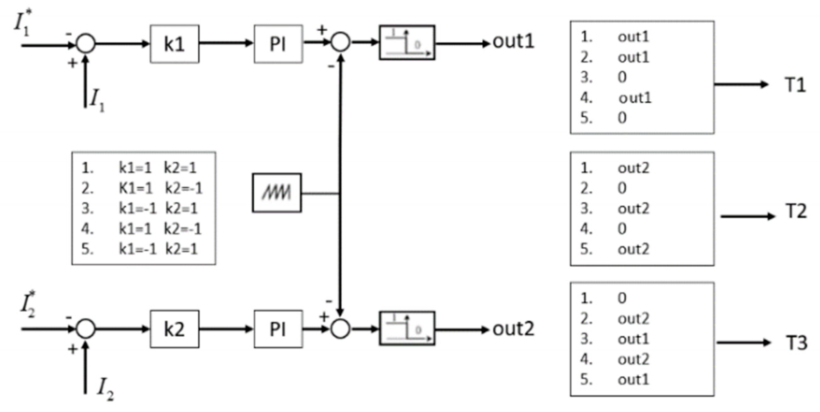
The control proposed in [32] is shown in Figure 2. It allows the converter to work in the DCM at low load (i.e., it prevents current inversion during the switching period), and it optimizes the current paths for loss reduction even in the CCM. The gains K1 and K2, and the connection between the outputs and the switch gate pulse vary, according to the working condition. Five working conditions are considered in the control described in Figure 2, as follows:
  • I 1 > 0 ,   I 2 > 0
  • I 1 > 0 ,   I 2 < 0
  • I 1 < 0 ,   I 2 > 0
  • I 1 < 0 ,   I 2 < 0 ,   I 1 > I 2
  • I 1 < 0 ,   I 2 < 0 ,   I 1 < I 2
Please note that i1 and i2 are the current instantaneous values, whereas I1 and I2 are the current average values during the duty cycle.
If both currents are positive, the instantaneous values are always different (i.e., current path D, shown in Figure 3, does not occur), and both currents work in the CCM. I transfer function between I1 and the duty cycle (m1) of switch T1 is given by (1):
I 1 m 1 = V o u t ( R 1 + s L 1 ) ( s T p + 1 )
where Vout is the output voltage, L1 and R1 are the inductance and resistance of the inductor in the series in regard to the storage, as shown in Figure 1, whereas Tp is the converter delay, which can be considered 1.5 times the switching period Ts. Please note that, as it is commonly set in the control of converters, this value of 1.5*Ts is the average between 1*Ts (the waiting time until the reference value of PWM changes) and 2*Ts (the time before the reference value changes plus an entire PWM period). An analogous equation correlates I2 with m2. Considering (1) that one can tune the PI controller gains using, for example, the phase margin criterion. However, with this set of gains, the current loop becomes significantly slow in the DCM (i.e., in the low-load region). Indeed, with the typical parameters of a converter, from (1) it follows that a small duty cycle variation leads to a significant current variation. On the contrary, in the DCM zone, as it is shown in Section 3, a significant duty cycle variation leads to a small current variation.
This study proposes a feed-forward technique to increase the converter dynamics at low load.

3. Feed-Forward Approach Derivation

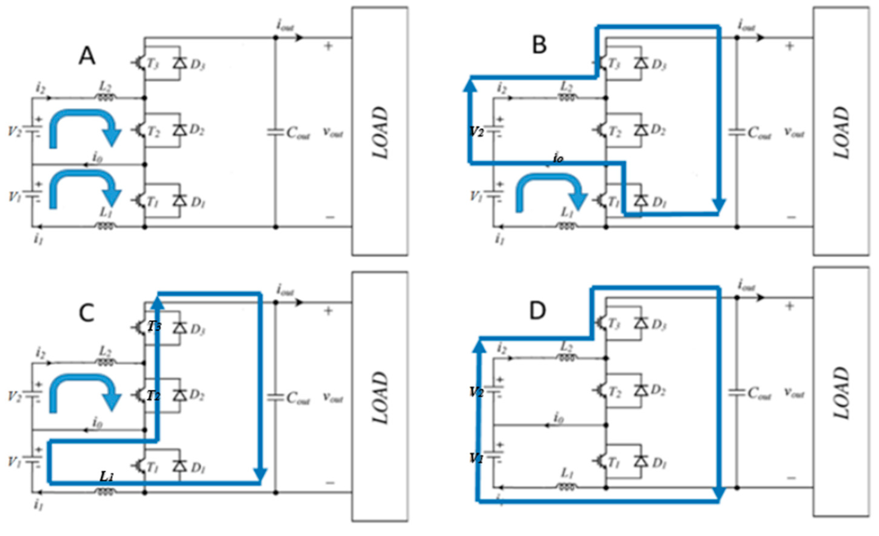
When both I1 and I2 are positive (condition 1), one has four different current paths, which are reported in Figure 3. In Table 1, expressions describing the different current slopes, which are the current derivatives during the switching period, and the IGBT configurations for each path, are shown.
As mentioned in Section 1 and Section 2, with the modulation strategy proposed in [32] and the converter working in the DCM, the dynamic response worsens significantly. In order to increase the dynamic behavior of the converter, it is therefore necessary to apply an opportune feed-forward technique. In this way, the feed-forward inputs guarantee a fast response, with a small error, which is then annulled by the PI controller, with a time constant that can be relatively high.
While working in the DCM, the relationship between the gate pulse duty cycles (GPDs) and the current references vary according to the current signs, the current values, depending on which current has a higher value. Not only does the relationship between the GPDs and current references vary according to the working condition, but, moreover, in regard to some working points (e.g., when current path D occurs), the analytic relationship becomes very complex and cannot be implemented in the converter control.
For these reasons, a simplified approach is carried out in this study, to find simplified relations between GPDs and current references.

3.1. Methodology

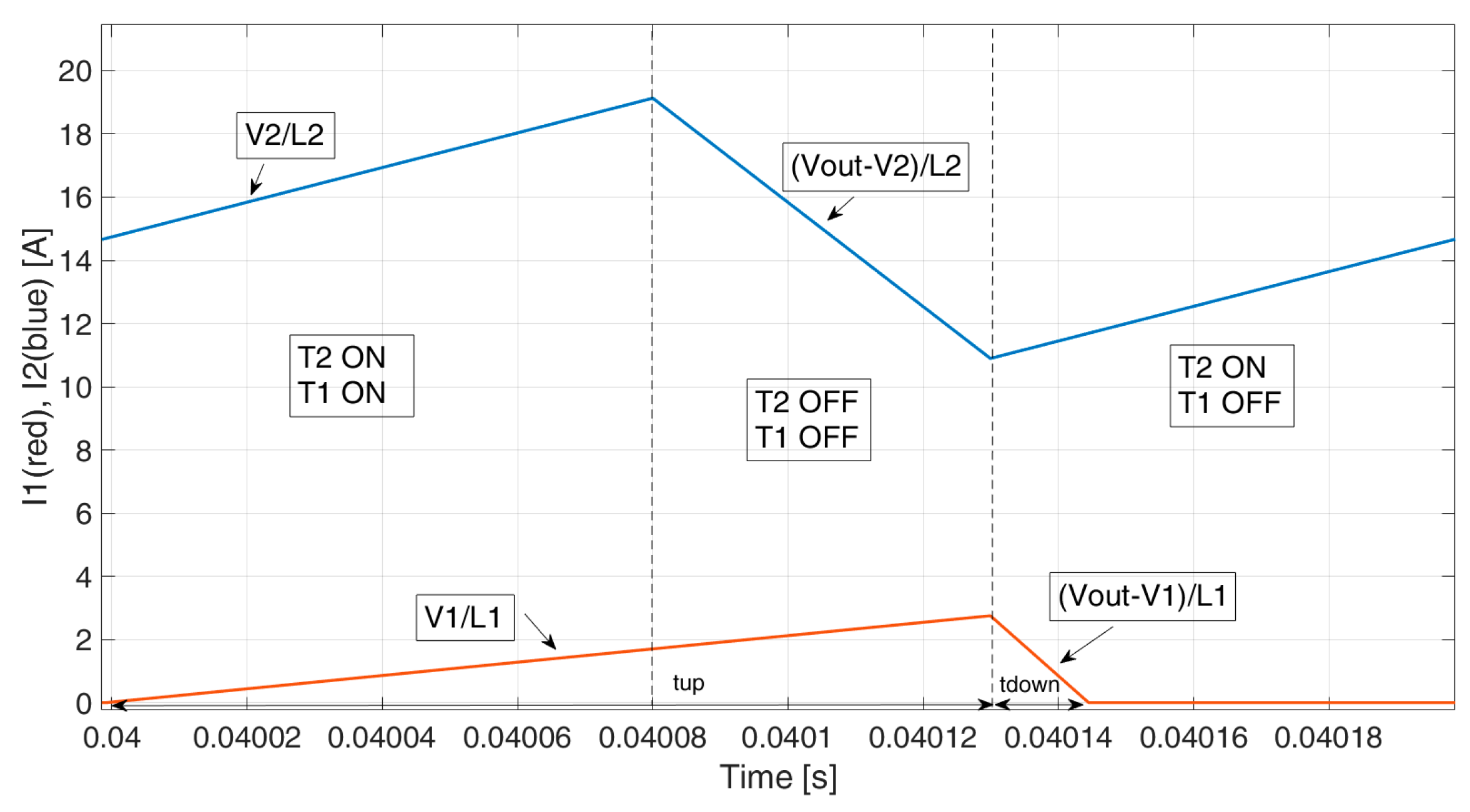
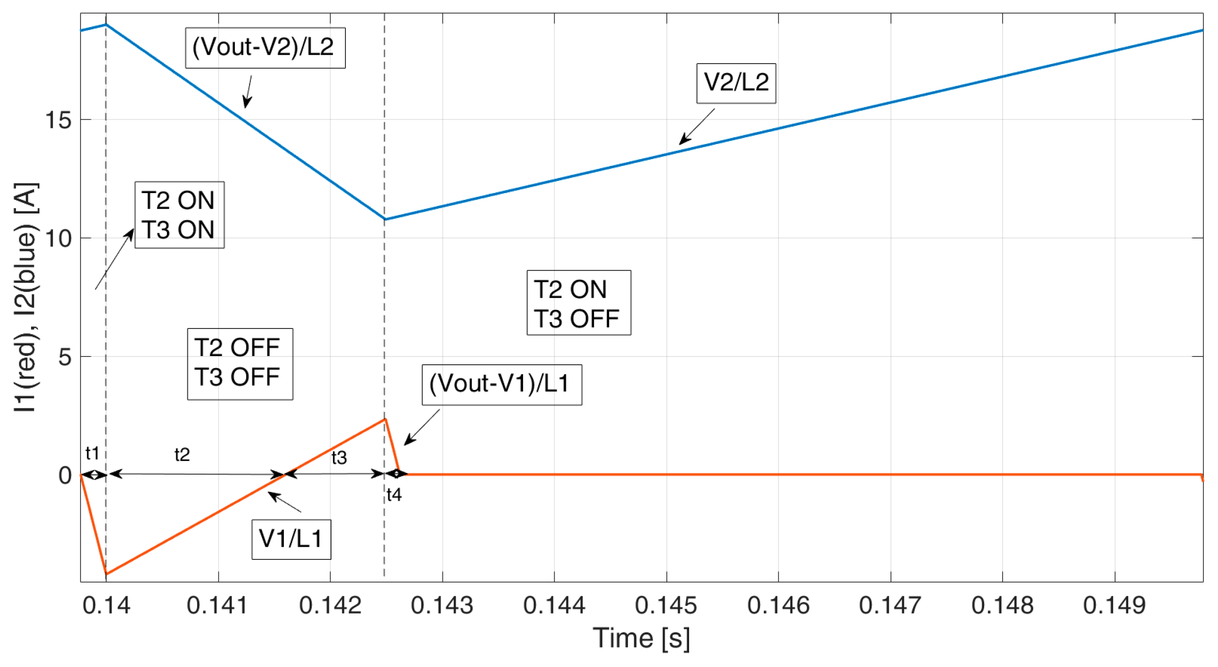
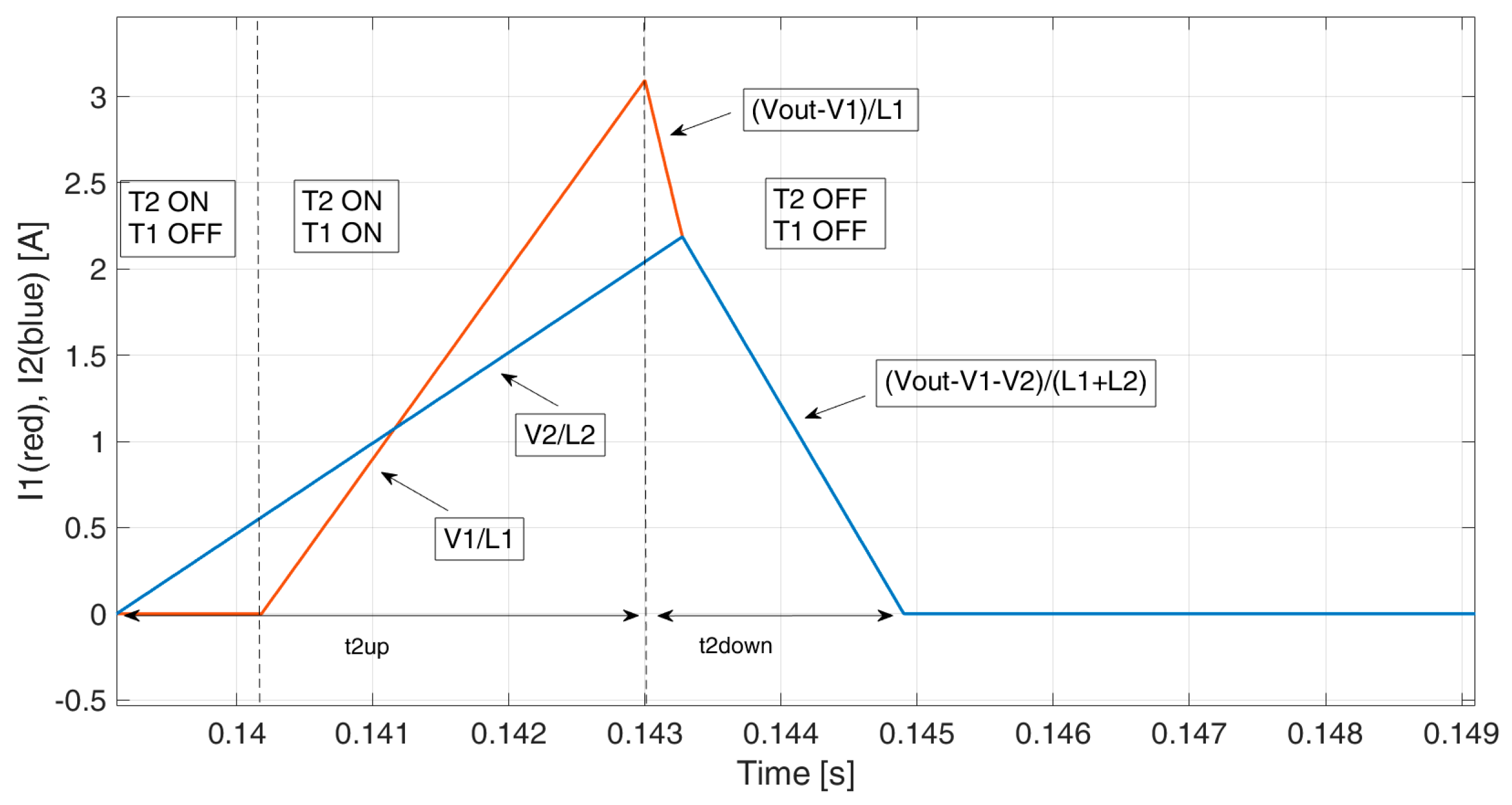
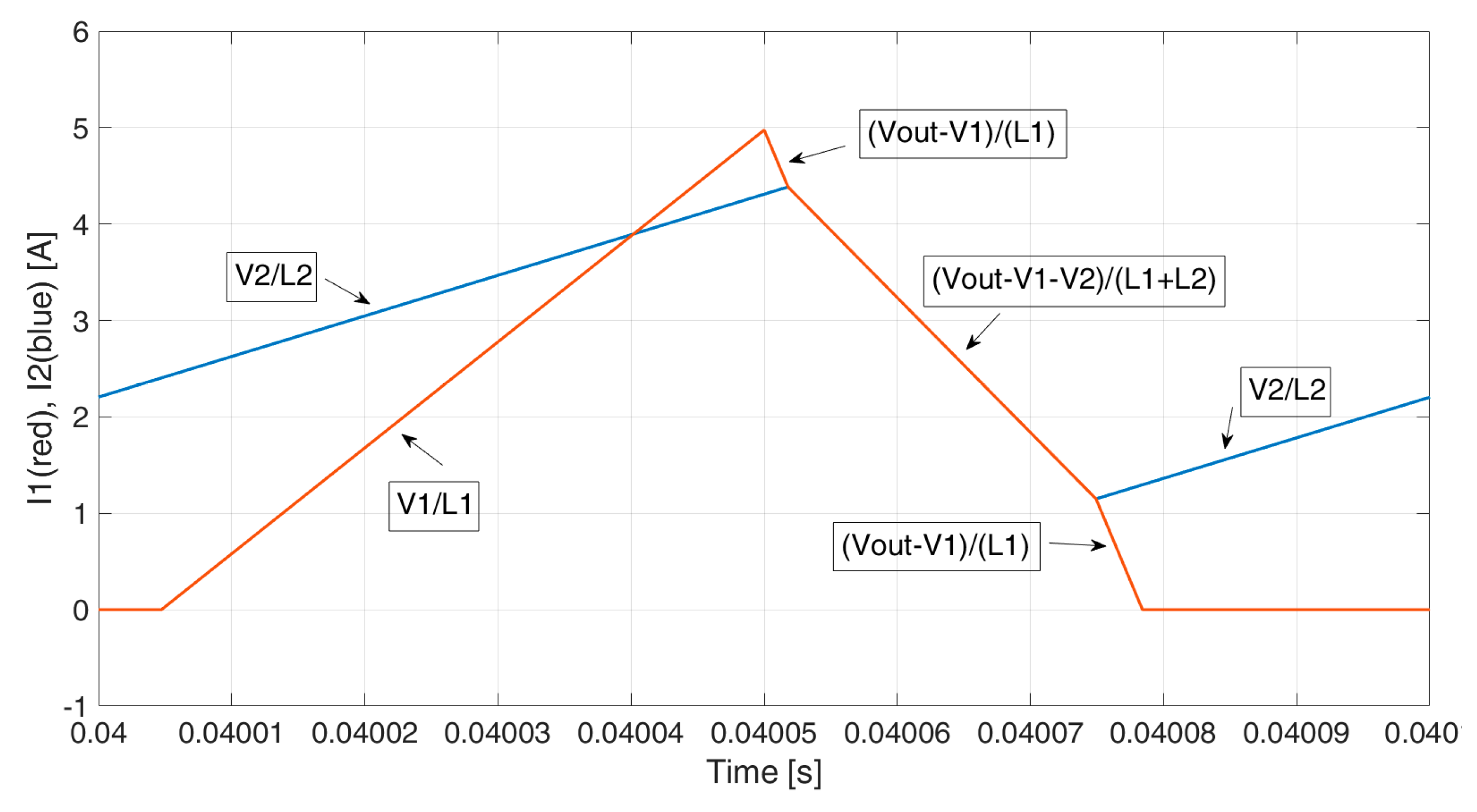
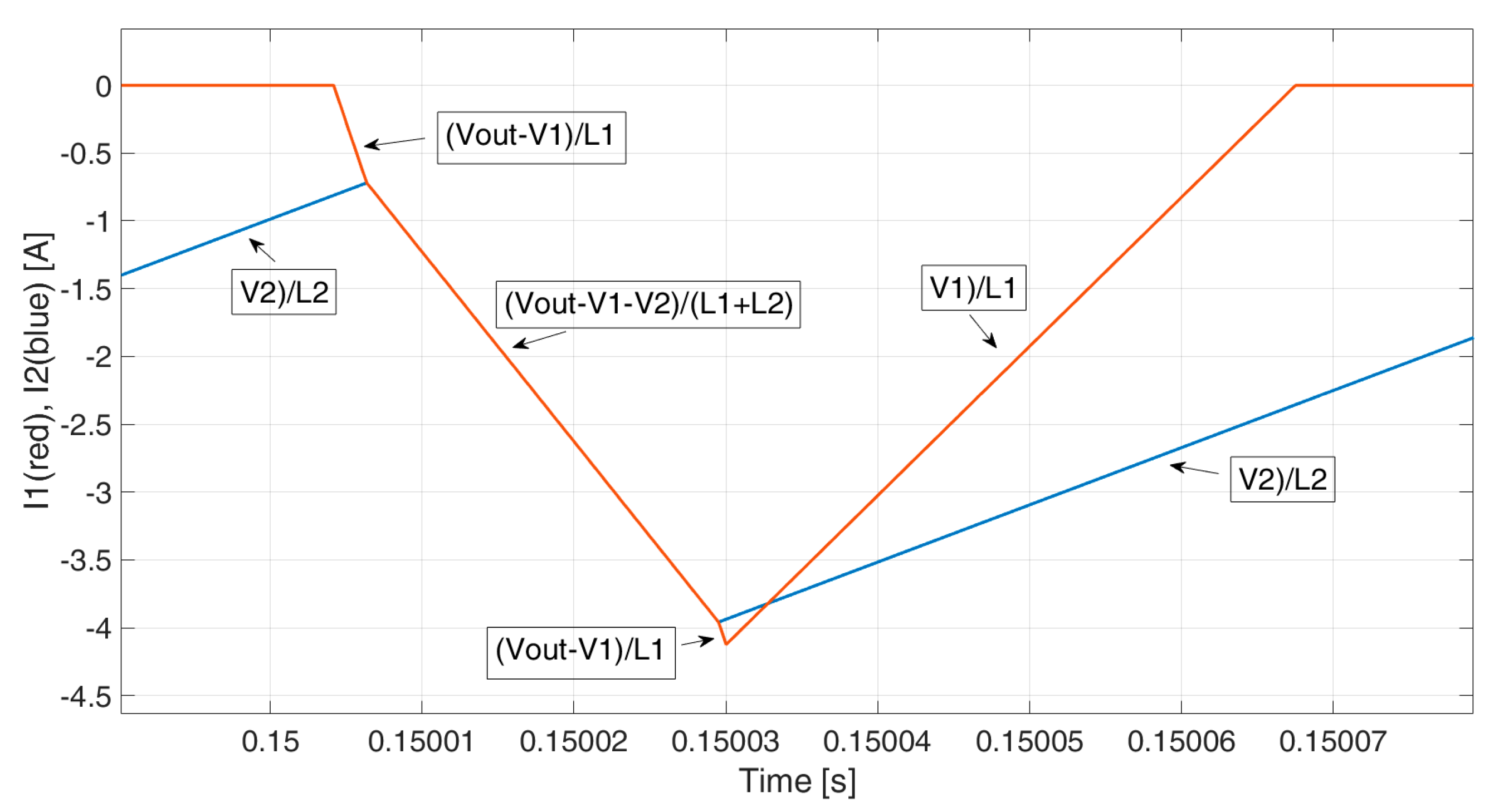
Figure 4 and Figure 5 show the instantaneous current waveforms, with i1 (red) and i2 (blue) positive and negative, respectively. One can note the current overlap in both cases. During the overlap (current path D in Figure 3), the current slopes become V o u t V 1 V 2 L 1 + L 2 , instead of V o u t V 1 L 1 and V o u t V 2 L 2 . Please note that current overlap (path D) occurs, while currents have the same instantaneous value and they are both decreasing, whereas, while both currents increase, the slopes are V 1 L 1 and V 2 L 2 , respectively (current path A).
From the current waveforms shown above, one can note that the analytic relations between the GPDs and current reference become very complex in these cases, and they depend on many variables. For this reason, a simplified approach is carried out in this paper, exploiting a simplified converter model.
The goal of the feed-forward method is to calculate the correct values for the three GPDs in order to satisfy the current references (i.e., to achieve certain average values for the two currents). The analytic equations are evaluated when there is no overlap (NOV) and when i1 = i2, i.e., when there is a total overlap (TOV). These two cases are identified as the two limit conditions. On such a basis, the equations obtained in these two cases are then interpolated to obtain the feed-forward values in the conditions with a partial overlap. Hence, a parameter K measuring the overlap ratio is defined.
The simplified converter model is obtained by evaluating six different conditions, as follows:
(1)
I 1 < I 2 ,   I 1 > 0 ,   I 2 > 0 (NOV and TOV)
(2)
I 1 < I 2 ,   I 1 < 0 ,   I 2 > I ^ 2 (NOV)
(3)
I 1 < I 2 ,   I 1 < 0 ,   I 2 < I ^ 2 (NOV and TOV)
(4)
I 1 > I 2 ,   I 1 > 0 ,   I 2 > 0 (NOV and TOV)
(5)
I 1 > I 2 ,   I 1 > I ^ 1 ,   I 2 > 0 (NOV)
(6)
I 1 > I 2 ,   I 1 < I ^ 1 ,   I 2 < 0 (NOV and TOV)
where I ^ 1 and I ^ 2 will be defined in the following Section and they are always positive quantities. For this reason, in the second and the fifth conditions, the currents have opposite signs and, therefore, an overlap is not possible. In this paper, only the first case was described in detail, contained in Appendix A, but the same procedure was used in this study to find the feed-forward outputs for the other five conditions.

3.2. Interpolation Process

The interpolation process is used to find the feed-forward output, while there is a partial overlap. The current ripples, when both currents are in the CCM and do not overlap, are defined in Equations (2) and (3). If the currents are in the DCM and there is no overlap, it is easy to verify that the ripple is given by (4) and (5). Therefore, a parameter K, which measures the overlap ratio, is defined in (6). Since in (A5), (A12), (A30), and (A38), the current is under the square root, the duty cycles can be calculated as in (7).
d i 1 = V 1 V o u t V 1 T s L 1 V o u t
d i 2 = V 2 V o u t V 2 T s L 2 V o u t
d i 1 r e a l = d i 1 I 1 d i 1 2 ( s i g n )     d i 1 r e a l d i 1 ; d i 1
d i 2 r e a l = d i 2 I 2 d i 2 2 ( s i g n )     d i 2 r e a l d i 2 ; d i 2
K = 2 ( I 2 I 1 ) d i 1 r e a l + d i 2 r e a l 0 ; 1
m x = K m x ( N O V ) + ( 1 K ) m x ( T O V )

4. Simulation Results

In this Section, some simulation results have been reported to compare the feed-forward (FF) method presented in this paper with the previous control in [30,32]. The system has been implemented in the MATLAB/Simulink/PLECS environment, and the converter parameters are reported in Table 2.
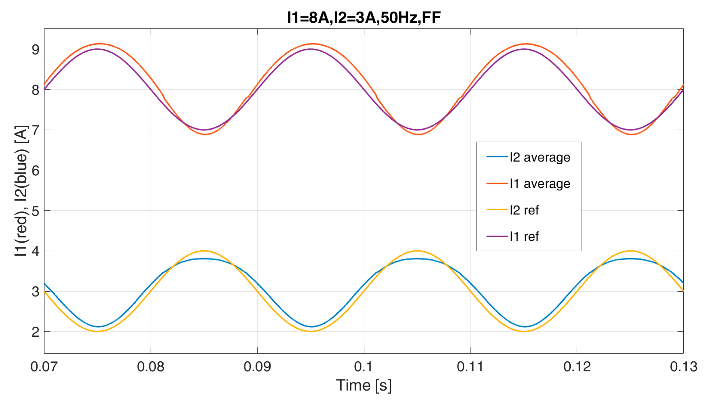
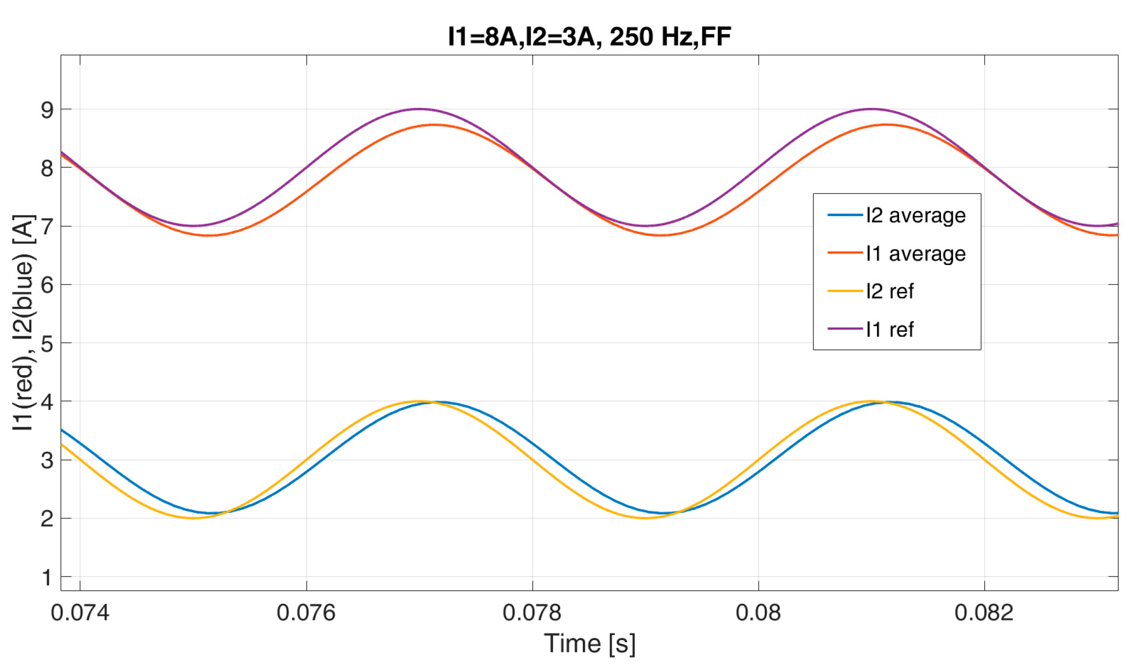
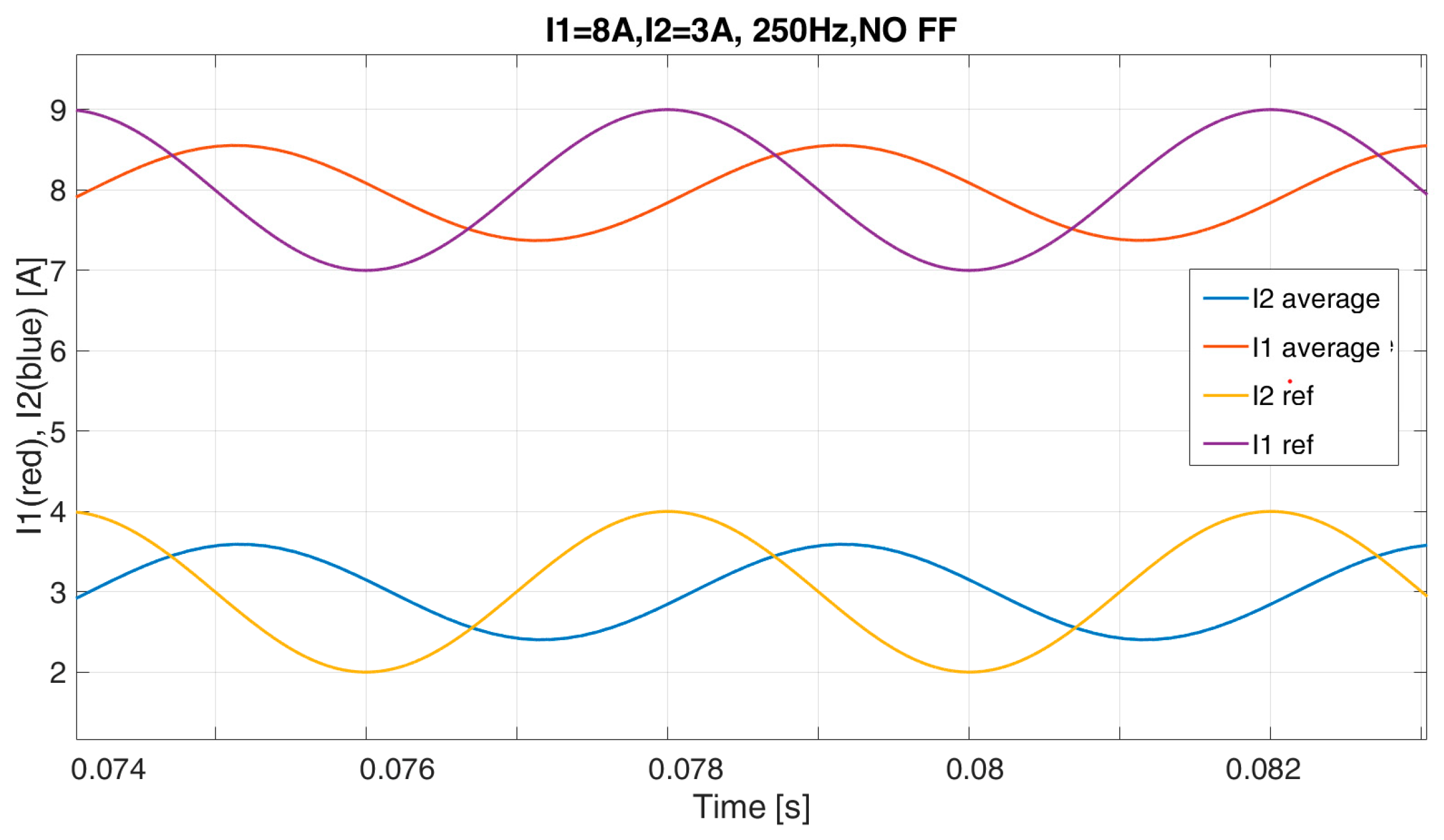
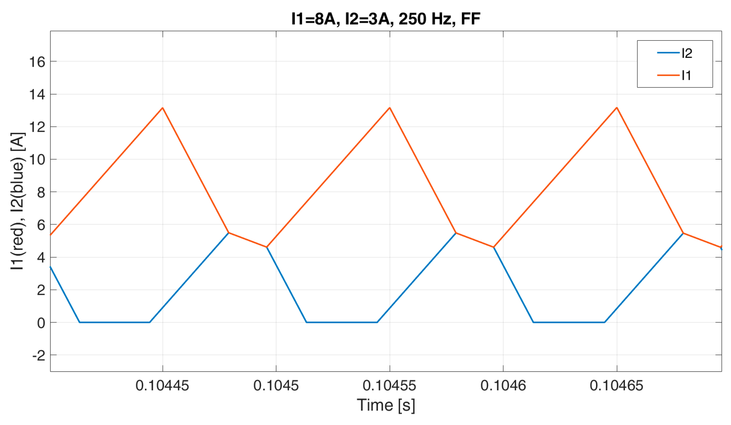
Two sinusoidal references have been imposed for I1 and I2, 8 A and 3 A, respectively (please note that 8 and 3 are the average values of the signal, the sine amplitude is 1), at the frequencies of 50 Hz and 250 Hz. In Figure 6 and Figure 7, the two average currents are shown together with their reference value, in the case of FF and NO FF, respectively, for the test at 50 Hz. Figure 8 and Figure 9 report the results for the test at 250 Hz, while in Figure 10 the two instantaneous values are reported in the case of FF at 250 Hz, where it can be seen that the two currents overlap and I2 is in the DCM.
From these simulation results it is possible to notice a better performance in the case of the proposed feed-forward method. As a matter of fact, in the 50 Hz test, the reference signal for I1 is not accurately followed in the case of NO FF in Figure 7, while a delay and an attenuation can be highlighted in the average currents in the test at 250 Hz, as reported in Figure 9.
In the following simulation tests a more critical working condition has been chosen, compared to the previous results. As a matter of fact, having both the two currents, the same small amplitude sinusoidal input as a reference leads the control to work close to the total overlap (TOV) condition in the DCM. In addition, every time the reference current crosses zero a discontinuity in the control is encountered.
The I2 waveform is plotted together with its reference both for the FF and NO FF control for a sinusoidal reference signal at 5 A (null average value in this case), and a 3 Hz frequency, as shown in Figure 11a,b. From the results it can be noticed that the reference is better in the case of the FF.
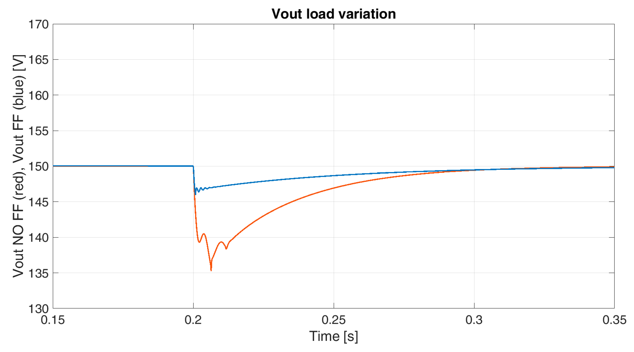
For the last simulation test, an outer voltage loop control has been implemented in order to keep the Vout at a constant value of 150 V, while the current reference I2 is kept at 5 A. Please note that the I1 reference is provided, instead, by the voltage control loop. The test involves a load step variation with a 100 Ω resistor connected to the DC link. The DC-link voltage is shown in Figure 12 both for FF and NO FF, where it is evident that the DC-link voltage drop is significantly reduced with the use of the proposed FF.
Please note that these last two simulations have been replicated in the Section 5 shown in the following Section and, the results are reported in Figure 19a,b, and Figure 20, respectively.

5. Experimental Results

In order to validate the proposed feed-forward (FF) approach, experimental tests were carried out in different operating conditions with both FF and NO FF. The test bench is shown in Figure 13. The control is implemented in a DSpace MicroLabBox (Paderborn, Germany). The Dspace system outputs are sent to the converter prototype, as illustrated in Figure 13. A supercapacitor (charged at 22 V) and a 12 V battery are used as the converter input sources. Please note that these values do not represent a realistic automotive application, since this converter prototype is a reduced-scale one (the development of a new converter prototype with a power level compatible with a typical automotive application and higher DC source voltage levels has already been taken into account for further studies). A 100 Ω resistor is connected to the DC link through a switch for load variation tests.
Since for this particular converter topology it is possible to control two quantities among I1, I2, and Vout, concerning the existing two degrees of freedom, all the experimental tests were performed with a current reference for I2 and a PI controller voltage loop to keep Vout at a constant value of 150 V.
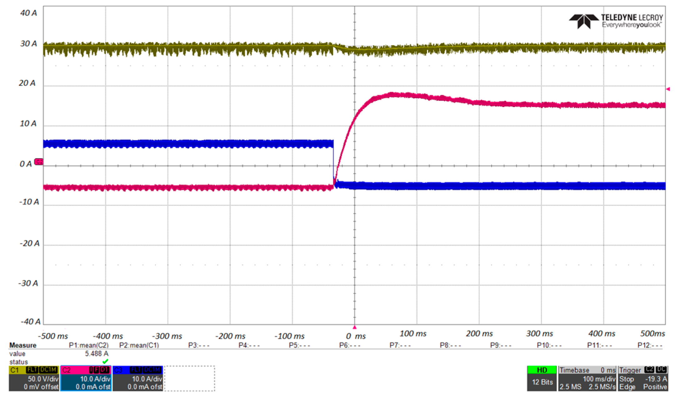
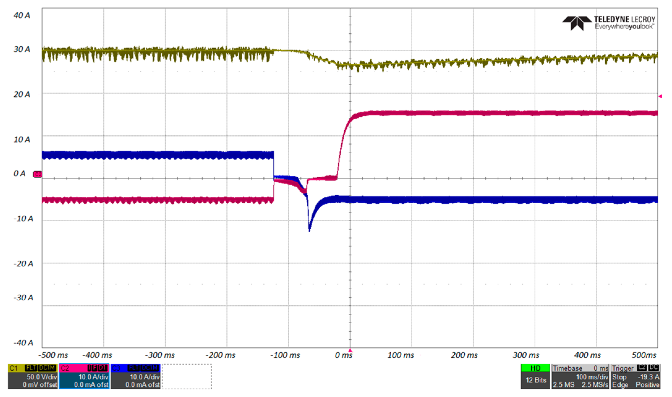
The I1 (magenta), I2 (blue), and Vout (green) are plotted in Figure 14 (FF) and Figure 15 (NO FF), with a current reference variation from +5 A to −5 A for I2 (blue line). Please note that the I1 reference is given by the voltage loop and I1 (magenta line) changes to keep a constant DC-link voltage.
It is clear that the control with the FF approach is way faster and more stable than the NO FF control. In the following, the plots show the measures exported from the Dspace interface, instead of oscilloscope measures, as in Figure 14 and Figure 15; this is done for two reasons, as follows:
  • A comparison between the I2 input reference current and the actual current I2 can be presented;
  • The Dspace interface computes the average value of a signal during a switching period, so a cleaner signal without ripples can be shown.
To determine the current control bandwidth in different working conditions, tests with a sinusoidal reference for I2 were carried out. Please note that for this experimental test a much more critical working condition has been chosen, compared to the simulation results. As a matter of fact, having a small amplitude sinusoidal input as a reference for the two currents leads the control to work close to the total overlap (TOV) condition in the DCM. In addition, every time the reference current crosses zero, a discontinuity in the control is encountered.
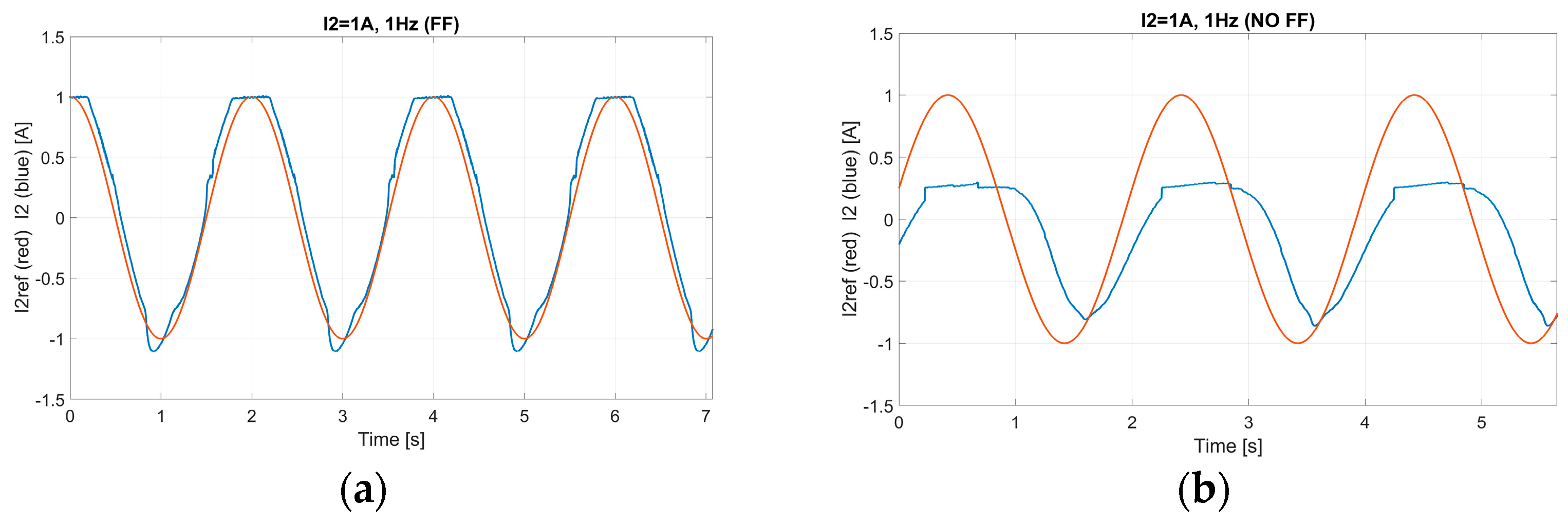
The I2 waveform is plotted, together with its reference both for the FF and NO FF control for a sinusoidal reference signal at 1 A, 1 Hz frequency, as shown in Figure 16a,b, and for a sinusoidal reference signal at 1 A, 3 Hz frequency, as shown in Figure 17a,b. Please note that the average I2 current limit for the DCM is given by (41) and it is 1.03 A, as reported in Table 2. Hence, the converter is fully working in the DCM for I2.
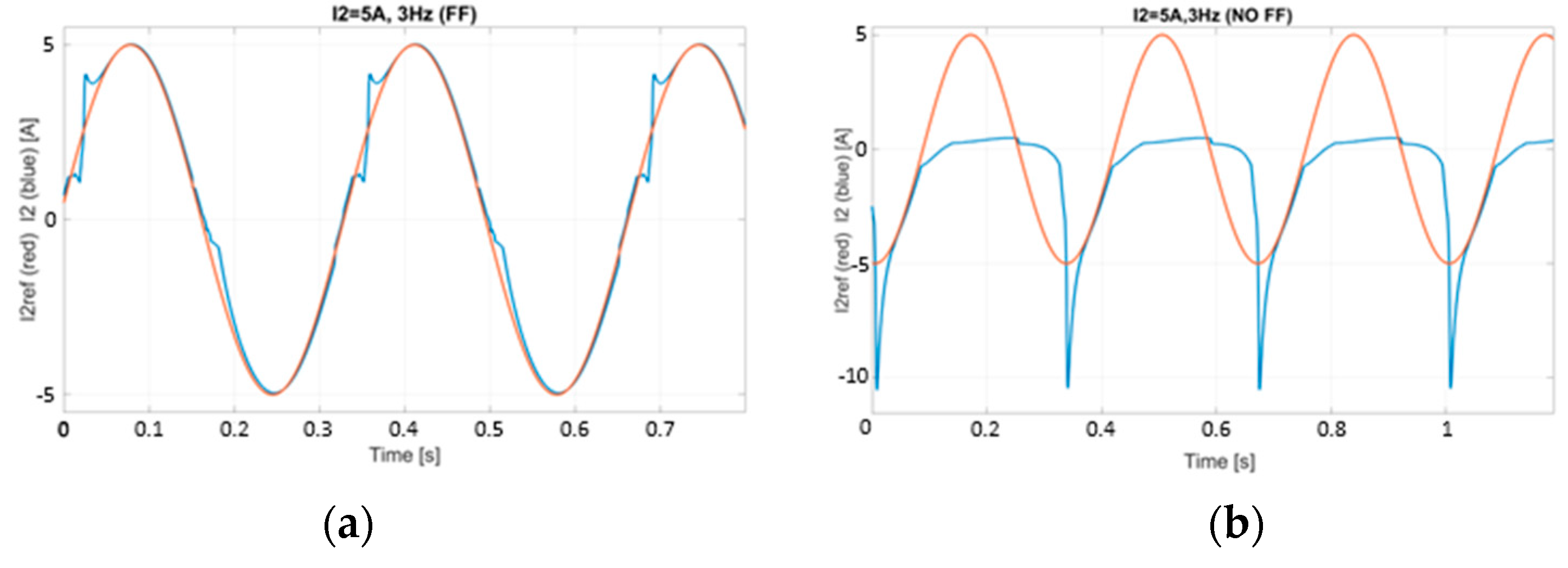
The same experiment has been carried out with a reference current amplitude of 5 A to test the converter working both in the CCM and in the DCM. The I2 waveform is plotted in Figure 18a,b for the test with 1 Hz frequency and in Figure 19a,b for the test at 3 Hz frequency. From the results shown in Figure 16, Figure 17, Figure 18 and Figure 19, it is easy to appreciate the benefits of the proposed FF approach compared to the previous control. As a matter of fact, the NO FF control is unstable with the reference signal at 3 Hz, while the FF control guarantees a good level of tracking of the reference signal.
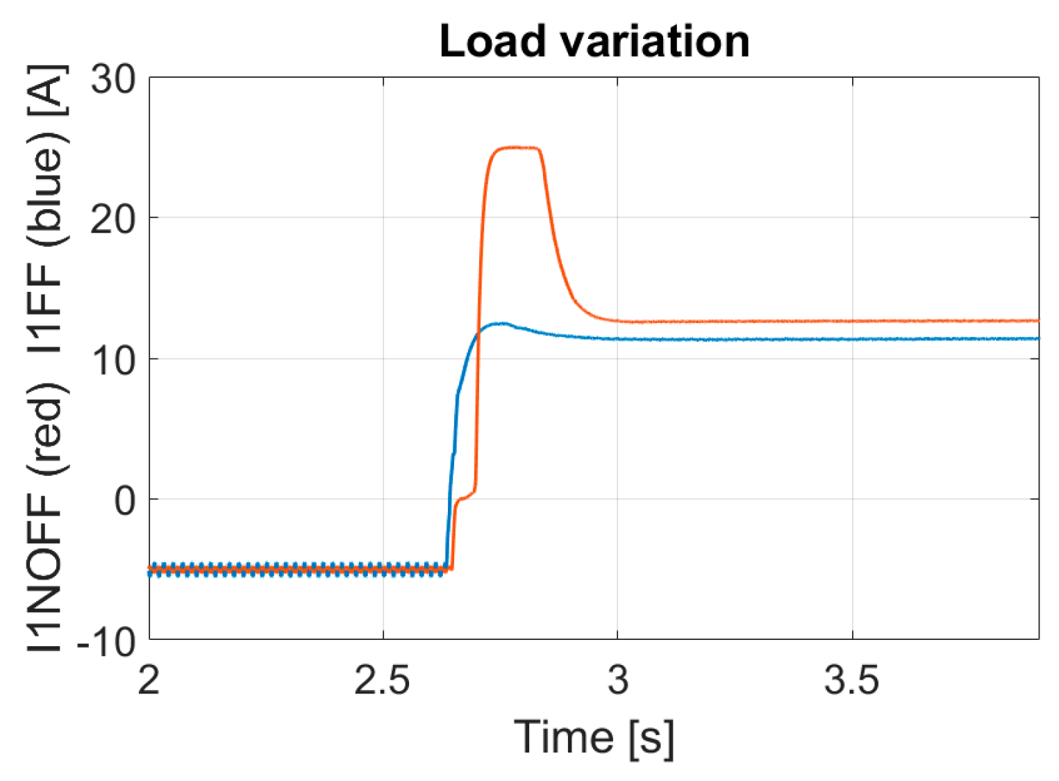
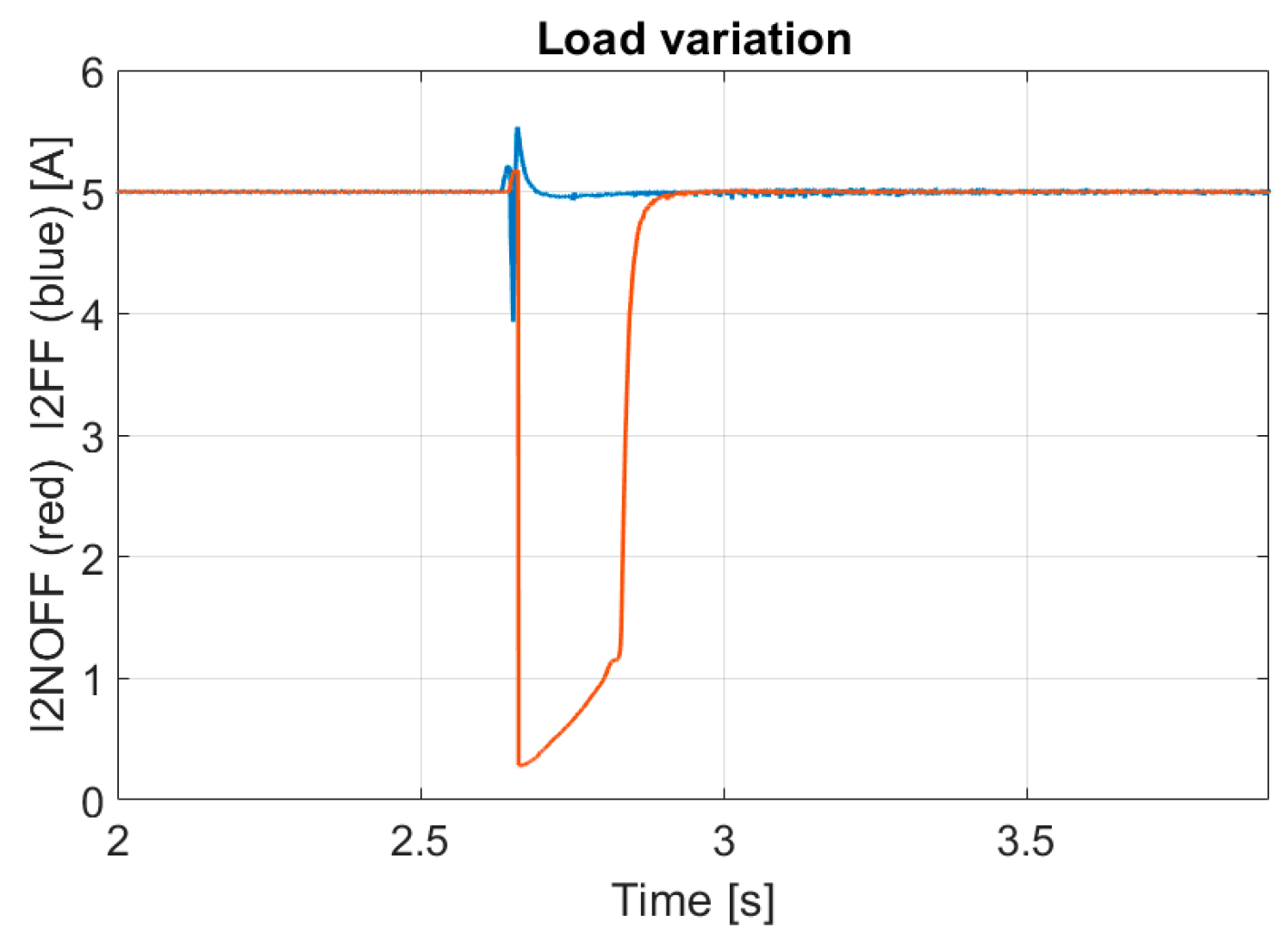
The last experimental test is a load step variation with a 100 Ω resistor connected to the DC link, while the current reference I2 is kept at 5 A; the I1 reference is provided, instead, by the voltage control loop. The DC-link voltage is shown in Figure 20, both for FF and NO FF, whereas the current waveforms are shown in Figure 21 and Figure 22. Please note that in Figure 20, Figure 21 and Figure 22, the signals of the different test acquisitions are superposed during the measure postprocessing. From Figure 20, it is clear that the DC-link voltage drop is significantly reduced, since the I1 current loop (Figure 21) is significantly faster with the FF control. Moreover, I2 remains almost constant with the FF, but drops significantly with NO FF (Figure 22).

6. Conclusions

In this paper, a new feed-forward strategy for a dual-input innovative three-switch DC–DC converter is proposed. The modulation strategy proposed in the literature for this particular topology exploited the DCM, increasing the overall efficiency of the system [32].
Since, in the DCM, the converter becomes highly non-linear, a simplified converter model is proposed in this study and used to implement the feed-forward control in the MATLAB/Simulink/PLECS environment, in order to perform simulation tests and provide a comparison with a previous control.
Afterwards, the proposed technique was implemented using a DSpace MicroLabBox, and experimental tests on a laboratory prototype were carried out to compare the feed-forward control proposed in this paper with the previous control proposed in the technical literature. Both the simulation and the experimental results reported show that the proposed feed-forward strategy exhibits advantages in terms of stability and dynamics compared to the control without the feed-forward approach, together with a more robust response regarding the voltage drop during the load step variation. Ultimately, please note that the modulating technique described in [32] increases the converter’s efficiency by allowing the exploitation of the DCM, but with undesirable dynamics; hence, the feed-forward approach presented in this paper is fundamental for the exploitation of the DCM control proposed in [32].

Author Contributions

Conceptualization, A.B., L.C., M.P. and S.C.; data curation, M.P. and S.C.; formal analysis, L.V. and M.P.; methodology, S.C. and M.P.; software, A.B., L.C., M.P. and S.C.; supervision, M.M., L.V. and S.S.; validation, L.V., S.S. and M.M.; writing—original draft, M.P.; writing—review and editing, M.P. and S.C. All authors have read and agreed to the published version of the manuscript.

Funding

This research received no external funding.

Data Availability Statement

The original contributions presented in the study are included in the article, further inquiries can be directed to the corresponding author.

Conflicts of Interest

The authors declare no conflicts of interest.

Appendix A

Appendix A.1. Case 1: I 1 < I 2 , I 1 > 0 , I 2 > 0

Appendix A.1.1. NOV, Equation for m2

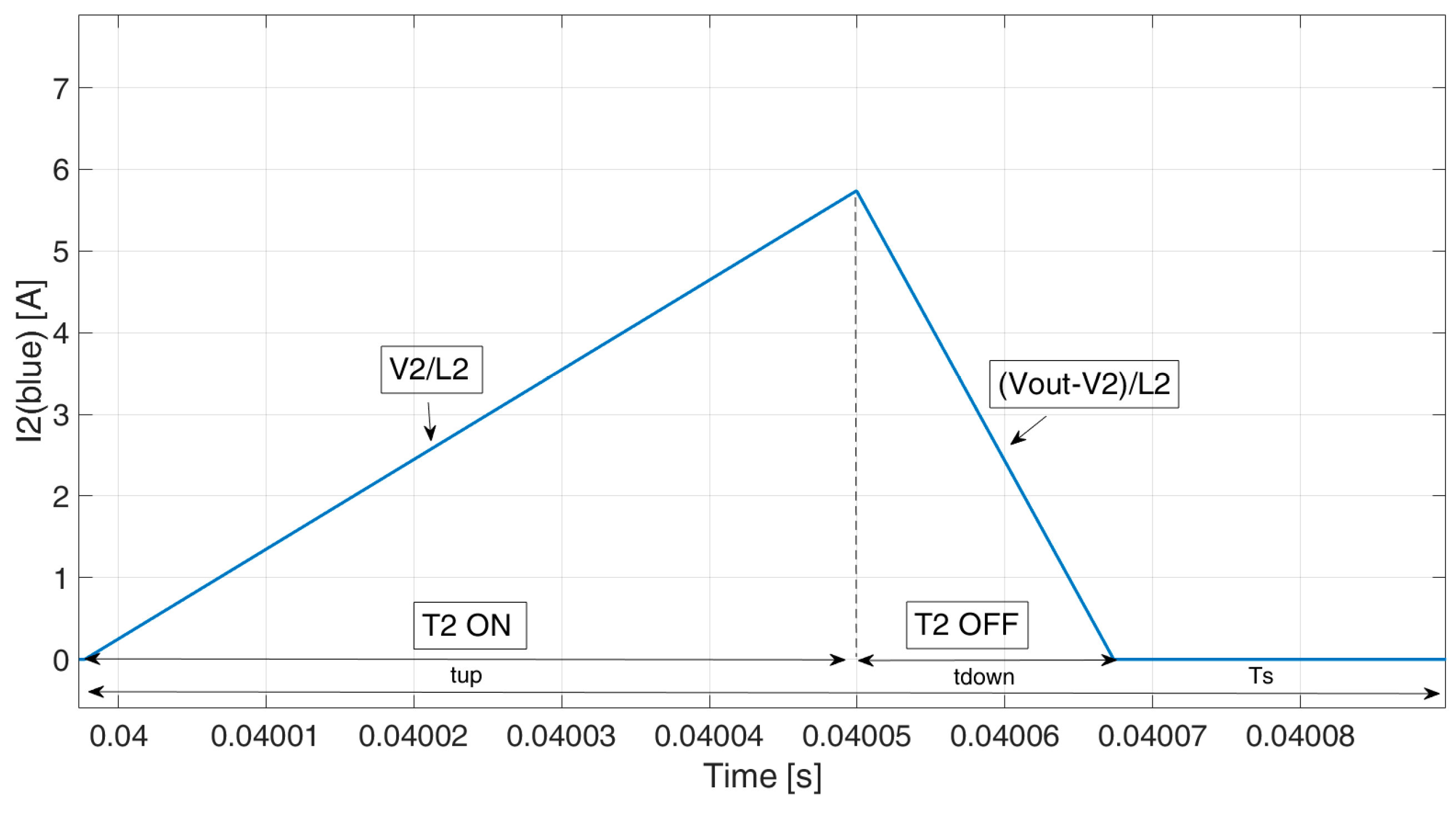
Firstly, the relationship between m2 and I2, while path D does not occur, will be evaluated. Please note that, in real cases, if I 1 > 0 and I 2 > 0 , condition D always occurs if i2 is in the DCM. The ideal i2 waveform is shown in Figure 6, whereas the real i2 waveform is shown in Figure A1. The equation obtained starting from the ideal waveform can be considered as the limit condition to be used in the interpolation process that is proposed below.
Figure A1. Ideal waveform of i2.
Energies 17 02170 g0a1
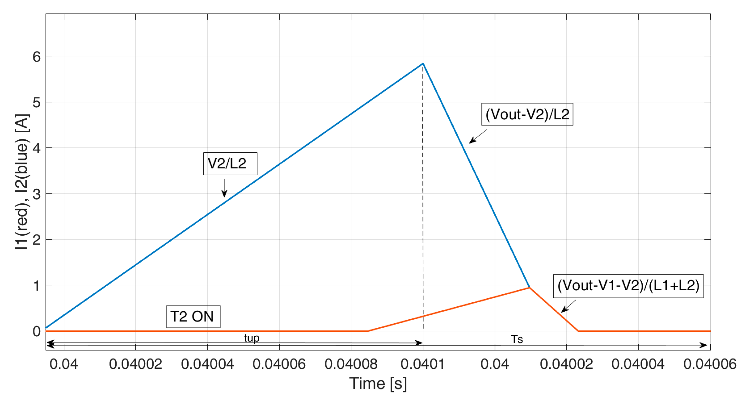
The i2 real waveform is shown in Figure A2, together with the i1 waveform. The rising time t u p is defined in (A1), the current peak value I p e a k is defined in (A2), the falling time t d o w n in (A3), whereas the average current I 2 is evaluated in (A4). Combining (A1), (A2), (A3), and (A4) obtains (A5).
t u p = m 2 × T s
I p e a k = V 2 L 2 × t u p
t d o w n = I p e a k V o u t V 2 L 2
I 2 = I p e a k × ( t u p + t d o w n ) 2 × T s
m 2 = 2 L 2 ( V o u t V 2 ) V 2 T s V o u t I 2
The relationship in (A5) is valid until i2 is in the DCM. Indeed, when the CCM occurs (i.e., when i2 does not reach zero during the switching period), the condition in (A6) should be verified. Substituting (A5) in (A6), one obtains (A7). Therefore, m2 is given by (A5), with the limitation that m 2 0 ; V o u t V 2 V o u t .
V 2 L 2 m 2 = V o u t V 2 L 2 ( 1 m 2 )
m 2 = V o u t V 2 V o u t
Figure A2. Real waveform of i1 (red) and i2 (blue).
Energies 17 02170 g0a2

Appendix A.1.2. NOV, I 1 > I 1 ^ Equation for m1

The i1 waveform is shown in Figure A3 (red), together with the i2 waveform (blue). Please note that to prevent a heavy notation with long subscripts, the definitions of t u p , t d o w n and I p e a k are valid from their definition until the next current waveform figure. Therefore, the same variable names are used at different times for different quantities. The t u p is now defined in (A8), I p e a k is defined in (A9), t d o w n in (A10), and the average current I 2 in (A11). Substituting (A8)–(A10) in (A11) obtains (A12).
Figure A3. The i1 (red) and i2 (blue) waveforms when I1 < 0 and I2 < 0 (condition 4).
Energies 17 02170 g0a3
t u p = ( m 1 + 1 m 2 ) T s
I 1 p e a k = V 1 L 1 t u p
t d o w n = I 1 p e a k V o u t V 1 L 1
I 1 = I 1 p e a k ( t u p + t d o w n ) 2 T s
m 1 = 2 L 1 ( V o u t V 1 ) T s V 1 V o u t I 1 + m 2 1
When the CCM occurs, the condition in (A13) should be verified. Substituting (A12) in (A13) obtains (A14).
Therefore, m1 is given by (A12), with the limitation that m 1 0 ; V o u t V 1 V o u t .
V 1 L 1 m 1 m 2 + 1 = V o u t V 1 L 1 ( m 2 m 1 )
m 1 = V o u t V 1 V o u t
It can be noted that when m1 = 0, i1 is not zero, since it increases while i2 is decreasing, as shown in Figure A4. The I1 value, while m1 = 0, is defined as I ^ 1, and it is calculated according to the following information.
Figure A4. The i1 (red) and i2 (blue) waveforms when I1 < 0 and I2 < 0 (condition 4).
Energies 17 02170 g0a4
The I1, while i2 is in the CCM and m1 = 0, defined as I ^ 1 N O V , can be evaluated substituting m1 = 0 and m 2 = V o u t V 2 V o u t  in (A12) obtaining (A15). While i2 tends towards zero,  also tends towards zero, as specified in (A16). The feed-forward value is given by the interpolation of I ^ 1 N O V and I ^ 1 T O V . The interpolation process is described in Section 3.2.
I ^ 1 N O V = T s V 1 V 2 2 2 L 1 V o u t ( V o u t V 1 )
I ^ 1 T O V = 0
The same process can be carried out to define I ^ 2 , I ^ 2 T O V , and I ^ 2 N O V .

Appendix A.1.3. NOV, I 1 < I ^ 1 Equation for m1

The current waveforms for the case where I 1 < I ^ 1 and there is NOV are shown in Figure A5. When I 1 < I ^ 1 , I 1  is controlled by m3 and t1 is defined in (A17), the i1 negative peak I 1 p e a k N e g is defined in (A18), t 2 and t 3 are defined in (A19) and (A20), the i1 positive peak value I 1 p e a k P o s is defined in (A21), and t 4 is defined in (A22). The average current I1 is defined in (A23).
Figure A5. The i1 (red) and i2 (blue) waveforms when I1 < 0 and I2 < 0 (condition 4).
Energies 17 02170 g0a5
t 1 = m 3 T s
I 1 p e a k N e g = t 1 V o u t V 1 L 1
t 2 = I 1 p e a k N e g V 1 L 1
t 3 = 1 m 2 t 2
I 1 p e a k P o s = V 1 L 1 t 3
t 4 = I 1 p e a k P o s V o u t V 1 L 1
I 1 = I 1 p e a k P o s t 3 + t 4 I 1 p e a k N e g ( t 1 + t 2 ) 2 T s
Substituting (A17)–(A22) in (A23), one obtains (A24).
m 3 = V 1 ( 1 m 2 ) 2 ( V o u t V 1 ) L 1 T s V o u t ( 1 m 2 ) I 1
Since Equation (25) is valid only when there is no superimposition (i.e., i2 is in the CCM), m 2 = V o u t V 2 V o u t , if one substitutes this value in (A24), one obtains (A25).
m 3 = V 1 V 2 2 V o u t ( V o u t V 1 ) L 1 T s V 2 I 1

Appendix A.1.4. TOV, Equation for m1 and m2

The other limit condition is when i1 = i2. Both current waveforms are reported in Figure A6. Neglecting the time in which one current is increasing and the other one is decreasing, one can derive (A26)–(A29), where the rising time t 2 u p , the current peak value I 2 p e a k , the falling time t 2 d o w n , and the average current I 2 are defined, respectively.
Figure A6. The i1 (red) and i2 (blue) waveforms when I1 < 0 and I2 < 0 (condition 4).
Energies 17 02170 g0a6
t 2 u p = m 2 T s
I 2 p e a k = V 2 L 2 t 2 u p
t 2 d o w n = I 2 p e a k V o u t V 1 V 2 L 1 + L 2
I 2 = I 2 p e a k ( t 2 u p + t 2 d o w n ) 2 T s
Combining (A26)–(A29), one obtains (A30).
m 2 = 2 L 2 2 ( V o u t V 1 V 2 ) V 2 T s ( L 1 V 2 L 2 V 1 + L 1 V o u t ) I 2
Equation (A30) is valid until i2 is in the DCM. Once i2 is in the CCM, the relationship in (A31) should be verified. Substituting (A26)–(A28) in (A31), one obtains (A32), which leads to the relationship in (A33). Therefore, m2 is given by (A30), with the limitation that m 2 0 ; L 2 ( V o u t V 1 V 2 ) ( L 1 V 2 L 2 V 1 + L 2 V o u t ) .
t 2 u p = t 2 d o w n
V 2 m 2 L 2 = V o u t V 1 V 2 L 1 + L 2 ( 1 m 2 )
m 2 = L 2 ( V o u t V 1 V 2 ) L 1 V 2 L 2 V 1 + L 1 V o u t
Moreover, t 1 u p , I 1 p e a k , t 1 d o w n , and I 1 are defined in (A34)–(A37). Substituting (A34)–(A36) in (A37), one obtains (A38).
t 1 u p = m 1 T s
I 1 p e a k = V 1 L 1 t 1 u p
t 1 d o w n = I 1 p e a k V o u t V 1 V 2 L 1 + L 2
I 1 = I 1 p e a k ( t 1 u p + t 1 d o w n ) 2 T s
m 1 = 2 L 1 2 T s V 1 V o u t V 1 V 2 L 2 V 1 L 1 V 2 + L 1 V o u t I 1
Since i1 = i2, the duty cycle should have the limitation m 1 0 ; m 2 . Please note that this limit is valid if V 2 L 2 < V 1 L 1 . If V 2 L 2 < V 1 L 1 , then m 1 0 ; L 1 ( V o u t V 1 V 2 ) ( L 2 V 1 L 1 V 2 + L 1 V o u t ) and m 2 0 ; m 1 .

References

  1. Fakham, H.; Lu, D.; Francois, B. Power Control Design of a Battery Charger in a Hybrid Active PV Generator for Load-Following Applications. IEEE Trans. Ind. Electron. 2011, 58, 85–94. [Google Scholar] [CrossRef]
  2. Manandhar, U.; Wang, B.; Zhang, X.; Beng, G.H.; Liu, Y.; Ukil, A. Joint Control of Three-Level DC–DC Converter Interfaced Hybrid Energy Storage System in DC Microgrids. IEEE Trans. Energy Convers. 2019, 34, 2248–2257. [Google Scholar] [CrossRef]
  3. Cha, H.; Choi, J.; Enjeti, P.N. A Three-Phase Current-Fed DC/DC Converter with Active Clamp for Low-DC Renewable Energy Sources. IEEE Trans. Power Electron. 2008, 23, 2784–2793. [Google Scholar] [CrossRef]
  4. Liang, Z.; Guo, R.; Li, J.; Huang, A.Q. A High-Efficiency PV Module-Integrated DC/DC Converter for PV Energy Harvest in FREEDM Systems. IEEE Trans. Power Electron. 2011, 26, 897–909. [Google Scholar] [CrossRef]
  5. Suryadevara, R.; Parsa, L. Full-Bridge ZCS-Converter-Based High-Gain Modular DC-DC Converter for PV Integration with Medium-Voltage DC Grids. IEEE Trans. Energy Convers. 2019, 34, 302–312. [Google Scholar] [CrossRef]
  6. Nathan, K.; Ghosh, S.; Siwakoti, Y.; Long, T. A New DC–DC Converter for Photovoltaic Systems: Coupled-Inductors Combined Cuk-SEPIC Converter. IEEE Trans. Energy Convers. 2019, 34, 191–201. [Google Scholar] [CrossRef]
  7. Hirose, T.; Matsuo, H. Standalone Hybrid Wind-Solar Power Generation System Applying Dump Power Control Without Dump Load. IEEE Trans. Ind. Electron. 2012, 59, 988–997. [Google Scholar] [CrossRef]
  8. Lai, C.-M.; Cheng, Y.-H.; Hsieh, M.-H.; Lin, Y.-C. Development of a Bidirectional DC/DC Converter with Dual-Battery Energy Storage for Hybrid Electric Vehicle System. IEEE Trans. Veh. Technol. 2018, 67, 1036–1052. [Google Scholar] [CrossRef]
  9. Benevieri, A.; Carbone, L.; Cosso, S.; Kumar, K.; Marchesoni, M.; Passalacqua, M.; Vaccaro, L. Series Architecture on Hybrid Electric Vehicles: A Review. Energies 2021, 14, 7672. [Google Scholar] [CrossRef]
  10. Lanzarotto, D.; Passalacqua, M.; Repetto, M. Energy comparison between different parallel hybrid vehicles architectures. Int. J. Energy Prod. Manag. 2017, 2, 370–380. [Google Scholar] [CrossRef]
  11. Passalacqua, M.; Lanzarotto, D.; Repetto, M.; Marchesoni, M. Conceptual design upgrade on hybrid pow ertrains resulting from electric improv ements. Int. J. Transp. Dev. Integr. 2018, 2, 146–154. [Google Scholar] [CrossRef]
  12. Su, G.-J.; Tang, L. A Multiphase, Modular, Bidirectional, Triple-Voltage DC–DC Converter for Hybrid and Fuel Cell Vehicle Power Systems. IEEE Trans. Power Electron. 2008, 23, 3035–3046. [Google Scholar] [CrossRef]
  13. Camara, M.B.; Gualous, H.; Gustin, F.; Berthon, A. Design and New Control of DC/DC Converters to Share Energy Between Supercapacitors and Batteries in Hybrid Vehicles. IEEE Trans. Veh. Technol. 2008, 57, 2721–2735. [Google Scholar] [CrossRef]
  14. Dell’Isola, D.; Urbain, M.; Weber, M.; Pierfederici, S.; Meibody-Tabar, F. Optimal Design of a DC–DC Boost Converter in Load Transient Conditions, Including Control Strategy and Stability Constraint. IEEE Trans. Transp. Electrif. 2019, 5, 1214–1224. [Google Scholar] [CrossRef]
  15. Shen, J.; Khaligh, A. A Supervisory Energy Management Control Strategy in a Battery/Ultracapacitor Hybrid Energy Storage System. IEEE Trans. Transp. Electrif. 2015, 1, 223–231. [Google Scholar] [CrossRef]
  16. Mamun, A.-A.; Liu, Z.; Rizzo, D.M.; Onori, S. An Integrated Design and Control Optimization Framework for Hybrid Military Vehicle Using Lithium-Ion Battery and Supercapacitor as Energy Storage Devices. IEEE Trans. Transp. Electrif. 2019, 5, 239–251. [Google Scholar] [CrossRef]
  17. Swaminathan, N.; Cao, Y. An Overview of High-Conversion High-Voltage DC–DC Converters for Electrified Aviation Power Distribution System. IEEE Trans. Transp. Electrif. 2020, 6, 1740–1754. [Google Scholar] [CrossRef]
  18. Wai, R.-J.; Lin, C.-Y.; Chang, Y.-R. High Step-Up Bidirectional Isolated Converter with Two Input Power Sources. IEEE Trans. Ind. Electron. 2009, 56, 2629–2643. [Google Scholar] [CrossRef]
  19. Heris, P.C.; Saadatizadeh, Z.; Babaei, E. A New Two Input-Single Output High Voltage Gain Converter with Ripple-Free Input Currents and Reduced Voltage on Semiconductors. IEEE Trans. Power Electron. 2019, 34, 7693–7702. [Google Scholar] [CrossRef]
  20. Matsuo, H.; Shigemizu, T.; Kurokawa, F.; Watanabe, N. Characteristics of the multiple-input DC-DC converter. In Proceedings of the IEEE Power Electronics Specialist Conference—PESC’93, Seattle, WA, USA, 20–24 June 1993; pp. 115–120. [Google Scholar] [CrossRef]
  21. Tao, H.; Duarte, J.L.; Hendrix, M.A.M. Three-Port Triple-Half-Bridge Bidirectional Converter with Zero-Voltage Switching. IEEE Trans. Power Electron. 2008, 23, 782–792. [Google Scholar] [CrossRef]
  22. Qian, Z.; Abdel-Rahman, O.; Batarseh, I. An Integrated Four-Port DC/DC Converter for Renewable Energy Applications. IEEE Trans. Power Electron. 2010, 25, 1877–1887. [Google Scholar] [CrossRef]
  23. Chen, G.; Jin, Z.; Deng, Y.; He, X.; Qing, X. Principle and Topology Synthesis of Integrated Single-Input Dual-Output and Dual-Input Single-Output DC–DC Converters. IEEE Trans. Ind. Electron. 2018, 65, 3815–3825. [Google Scholar] [CrossRef]
  24. Ganjavi, A.; Ghoreishy, H.; Ahmad, A.A. A Novel Single-Input Dual-Output Three-Level DC–DC Converter. IEEE Trans. Ind. Electron. 2018, 65, 8101–8111. [Google Scholar] [CrossRef]
  25. Liu, Y.-C.; Chen, Y.-M. A Systematic Approach to Synthesizing Multi-Input DC–DC Converters. IEEE Trans. Power Electron. 2009, 24, 116–127. [Google Scholar] [CrossRef]
  26. Ray, O.; Josyula, A.P.; Mishra, S.; Joshi, A. Integrated Dual-Output Converter. IEEE Trans. Ind. Electron. 2015, 62, 371–382. [Google Scholar] [CrossRef]
  27. Shanthi, T.; Prabha, S.U.; Sundaramoorthy, K. Non-Isolated n-Stage High Step-up DC-DC Converter for Low Voltage DC Source Integration. IEEE Trans. Energy Convers. 2021, 36, 1625–1634. [Google Scholar] [CrossRef]
  28. Wai, R.-J.; Lin, C.-Y.; Chen, B.-H. High-Efficiency DC–DC Converter with Two Input Power Sources. IEEE Trans. Power Electron. 2012, 27, 1862–1875. [Google Scholar] [CrossRef]
  29. Marchesoni, M.; Vacca, C. New DC–DC Converter for Energy Storage System Interfacing in Fuel Cell Hybrid Electric Vehicles. IEEE Trans. Power Electron. 2007, 22, 301–308. [Google Scholar] [CrossRef]
  30. Marchesoni, M.; Passalacqua, M.; Vaccaro, L. A Refined Loss Evaluation of a Three-Switch Double Input DC-DC Converter for Hybrid Vehicle Applications. Energies 2020, 13, 204. [Google Scholar] [CrossRef]
  31. Benevieri, A.; Carbone, L.; Cosso, S.; Gallione, F.; Hussain, S. Multi-Input Bidirectional DC-DC Converter for Energy Management in Hybrid Electrical Vehicles Applications. In Proceedings of the 2023 13th International Symposium on Advanced Topics in Electrical Engineering (ATEE), Bucharest, Romania, 23–25 March 2023; pp. 1–5. [Google Scholar] [CrossRef]
  32. Passalacqua, M.; Marchesoni, M.; Vaccaro, L. A New Modulation Strategy for Exploiting Discontinuous Conduction Mode in a Double-Input Three-Switch Bidirectional DC–DC Converter. IEEE Trans. Ind. Electron. 2020, 68, 10815–10825. [Google Scholar] [CrossRef]
Figure 1. Three-switch dual-input bidirectional DC–DC converter.
Energies 17 02170 g001
Figure 2. The control scheme for the three-switch converter.
Energies 17 02170 g002
Figure 3. Current paths in condition 1 (I1 and I2 > 0). (A) Path A; (B) Path B; (C) Path C; (D) Path D.
Energies 17 02170 g003
Figure 4. The i1 (red) and i2 (blue) waveforms when I1 > 0 and I2 > 0 (condition 1) in condition 1 (I1 and I2 > 0).
Energies 17 02170 g004
Figure 5. The i1 (red) and i2 (blue) waveforms when I1 < 0 and I2 < 0 (condition 4).
Energies 17 02170 g005
Figure 6. Simulated average currents I1 and I2 with their reference values at 50 Hz, FF.
Energies 17 02170 g006
Figure 7. Simulated average currents I1 and I2 with their reference values at 50 Hz, NO FF.
Energies 17 02170 g007
Figure 8. Simulated average currents I1 and I2 with their reference values at 250 Hz, FF.
Energies 17 02170 g008
Figure 9. Simulated average currents I1 and I2 with their reference values at 250 Hz, NO FF.
Energies 17 02170 g009
Figure 10. Simulated instantaneous currents I1 and I2, with their reference values at 250 Hz, FF.
Energies 17 02170 g010
Figure 11. Simulated current I2 and the reference, 5 A, 3 Hz: (a) with FF, (b) without FF.
Energies 17 02170 g011
Figure 12. Simulated Vout FF (blue) and NO FF (red) during a load step variation.
Energies 17 02170 g012
Figure 13. Test bench.
Energies 17 02170 g013
Figure 14. The Vout (green, C1, 50 V/div), i1 (magenta, C2, 10 A/div), and i2 (blue, C3, 10 A/div) during an I2 variation from +5 A to −5 A (FF).
Energies 17 02170 g014
Figure 15. The Vout (green, C1, 50 V/div), i1 (magenta, C2, 10 A/div), and i2 (blue, C3, 10 A/div) during an I2 variation from +5 A to −5 A (NO FF).
Energies 17 02170 g015
Figure 16. Experimental current I2 and the reference, 1 A, 1 Hz: (a) with FF, (b) without FF.
Energies 17 02170 g016
Figure 17. Experimental current I2 and the reference, 1 A, 3 Hz: (a) with FF, (b) without FF.
Energies 17 02170 g017
Figure 18. Experimental current I2 and the reference, 5 A, 1 Hz: (a) with FF, (b) without FF.
Energies 17 02170 g018
Figure 19. Experimental current I2 and the reference, 5 A, 3 Hz: (a) with FF, (b) without FF.
Energies 17 02170 g019
Figure 20. The Vout FF (blue) and NO FF (red) during a load step variation.
Energies 17 02170 g020
Figure 21. The I1 with FF (blue) and NO FF (red) during a load step variation.
Energies 17 02170 g021
Figure 22. The I2 with FF (blue) and NO FF (red) during a load step variation.
Energies 17 02170 g022
Table 1. Current slopes and IGBT configuration in condition 1.
PathIGBT Config.Current Slope I1Current Slope I2
AT1 on
T2 on
T3 off
V 1 L 1 V 2 L 2
BT1 on (or T1 off and i1 < i2)
T2 off
T3 off
V 1 L 1 V o u t V 2 L 2
CT1 off
T2 on (or T2 off and i2 < i1)
T3 off
V o u t V 1 L 1 V 2 L 2
DT1 off
T2 off
T3 off
V o u t V 1 V 2 L 1 + L 2 V o u t V 1 V 2 L 1 + L 2
Table 2. Converter parameters.
ParameterValueParameterValue
IGBT typeSKM400GA124DC4.7 mF
V112 VVout150 V
L1950 µHfsw10 kHz
L2910 µHI1 limit0.55 A
V222 VI2 limit1.03 A
R10.01 ΩR20.01 Ω
Disclaimer/Publisher’s Note: The statements, opinions and data contained in all publications are solely those of the individual author(s) and contributor(s) and not of MDPI and/or the editor(s). MDPI and/or the editor(s) disclaim responsibility for any injury to people or property resulting from any ideas, methods, instructions or products referred to in the content.