Article

A Soft-Switching Proportional Dimming LED Driver Based on Switched Capacitor

Hubei Collaborative Innovation Center for High-Efficiency Utilization of Solar Energy, Hubei University of Technology, Wuhan 430070, China
*
Author to whom correspondence should be addressed.
Energies 2024, 17(6), 1368; https://doi.org/10.3390/en17061368
Submission received: 25 January 2024 / Revised: 23 February 2024 / Accepted: 28 February 2024 / Published: 12 March 2024
(This article belongs to the Section F: Electrical Engineering)

Abstract

:
This paper proposes a switched capacitor-based soft-switching proportional dimming LED driver to address color-mixing LED applications. The driver utilizes a half-bridge switch structure and incorporates a switched capacitor to regulate the dual resonant network. This configuration facilitates current sharing across each resonant network and enables fixed proportion dimming between them. The common inductance leveraged in this design results in fewer switching devices, thereby enhancing efficiency. Furthermore, all switches and diodes achieve soft switching, contributing to high efficiency. Finally, this paper built a 19 W experimental prototype, and the maximum efficiency reached 95.56%, which verified the correctness and feasibility of the driver.

1. Introduction

In recent years, light-emitting diodes (LEDs) have rapidly advanced due to their energy-saving, environmental-friendly, long-lasting, and flexible attributes, making them extensively utilized in commercial, residential, and industrial lighting [1,2]. LEDs offer versatility in terms of their form factor and are often employed in series and parallel connections. For applications in plant factory lighting systems, LED lamps are preferred over natural lighting for plant growth, due to their cost effectiveness, high power efficiency, and specialized spectrum [3,4]. The predominant red and blue light ratio utilized in plant growth LED lamps necessitates a specific current-dimming proportion for multi-channel LED drivers, making it essential to investigate the current control of multi-channel output LED drivers. The volt–ampere characteristics of LEDs link the luminous efficiency to the forward current, leading to the prevalent use of a constant current drive to ensure balanced luminous intensity across branches. Current-controllable multi-channel LED drivers are primarily designed for multi-color lighting and color-mixing applications, necessitating the capability to output current across multiple channels while preserving an adjustable current accuracy.
References [5,6] discuss the implementation of single-inductor multiple-output (Simo) LED drivers for achieving current control and dimming operation. Reference [5] introduces a Simo LED driver structure with time reuse control but is hampered by a limitation on the maximum controllable current and a reduction in the number of LED strings. Reference [6] presents a current source mode Simo LED driver with independent dimming, yet its hard-switched switch tube leads to switching losses. Reference [6] introduces a dual-output LED driver based on coupled inductors, though it poses challenges in determining the load rating, since one of the loads is powered by leakage inductance, despite achieving soft switching. A noteworthy characteristic of these LED drivers is the exclusive use of inductors and memory [5,6].
Literature [7] proposes a dual-output LED driver based on coupled inductance. Although soft switching can be realized, the load rating is not well determined because one of the loads is powered by the leakage sense. These LED drives are characterized by the use of inductors, hard switch, dimming control, and other problems. LED drivers commonly employ half-bridge and full-bridge resonant converters, due to their simple design, soft-switching capabilities, and inherent constant current (CC) characteristics. For instance, reference [8] introduces a high-gain circuit topology that integrates buck-boost and half-bridge series resonant converters, enabling the adjustment of output current by changing the frequency of an additional dimming switch. However, the challenge arises when the LED load branch increases, presenting difficulties in dimming control. In contrast, reference [9] presents a variable mode LED driver that combines buck-boost and full-bridge LLCs, achieving three distinct voltage gains by modifying the switch combination on the inverter side but with reduced overall efficiency due to the cascade structure. Additionally, reference [10] suggests a continuous conduction mode (CCM) boost and LLC resonant network integration, but it is limited by its single-stage converter that can only drive one load. Similarly, reference [11] proposes a dimmable LED driver based on an LCLC network, in which the auxiliary switch’s buffer capacitor affects output current accuracy while providing soft switching. Moreover, references [12,13] introduce an LED multi-channel current-sharing topology, employing controllable switched capacitors to enable a wide dimming range, albeit at the cost of increasing the number of switches and passive components. Literature [14] deals with a design and experimental verification of a 400 W class light-emitting diode (LED) driver with the cooperative control method for two parallel, connected DC/DC converters. In the cooperative control method, one DC/DC converter is selected to supply the output current for the LED, based on the reference value of the LED current. Thus, the proposed cooperative control strategy achieves wide dimming range operation, but with reduced overall efficiency due to the cascade structure. Literature [15] puts forth a three-switch, double half-bridge, double-output LED driver, utilizing asymmetric duty cycle control to adjust output current but encountering the issue of diode inability to achieve soft switching, leading to significant diode conduction losses.
In order to solve the problems of LED multi-channel current-sharing topology dimming and low efficiency, this paper proposes a four-channel constant proportion dimming LED driver based on an integrated half-bridge resonant switching network. In this network, switches S1 and S2 in the half-bridge display complementary conduction, while the controllable switched capacitor unit’s switch S3 and switch S2 share the same drive signal. The constant frequency pulse width modulation (PWM) controls four current outputs. The converter’s working mode and dimming strategy are discussed in detail. Through the utilization of only one common inductor, the driver enables the simultaneous soft switching of switching tubes and diodes, allowing the upper and lower groups of LED current-sharing output units to proportionally adjust light and current.

2. Analysis of Circuit Structure and Working Principle

2.1. Topology

In Figure 1, the integrated half-bridge resonant switching unit comprises switching tubes S1 and S2, common inductance LS, and resonant capacitors Cr1 and Cr2, as well as controllable switching capacitor units, which include switching tube S3 and switching capacitor CS1. This unit serves as the foundation for the soft-switching proportional dimming LED driver based on switched capacitors. Moreover, two LED current-sharing output units are depicted in the figure. The first unit consists of freewheeling diodes D1–D4, filter capacitors Co1–Co2, and output loads LED1–LED2, while the second unit encompasses freewheeling diodes D5–D8, filter capacitors Co3–Co4, and output loads LED3–LED4. Together, these components establish the topology of the LED driver, facilitating the implementation of soft-switching proportional dimming for efficient LED control.

2.2. Operational Modal Analysis

To simplify the analysis, we assume that all switches, diodes, capacitors, and inductors in the system are ideal components and that the values of resonant capacitors Cr1 and Cr2 are lower than those of filter capacitors Co1, Co2, Co3, and Co4, resulting in constant values for VLED1~VLED4. Figure 2 presents the key waveforms of the proposed converter. The intermediate voltage values of resonant capacitors Cr1 and Cr2 are denoted by VCr1 and VCr2, respectively. Throughout the entire cycle, the converter operates in six modes, each corresponding to an equivalent circuit diagram depicted in Figure 3a through Figure 3f.
Mode 1 [t0~t1]: At time t0, when switch tubes S2 and S3 are simultaneously turned on and switch tube S1 remains off, diodes D1, D3, D5, and D7 conduct in the forward direction, while diodes D2, D4, D6, and D8 are cut off in the reverse direction. The common inductor current ILS drops to zero under back voltage, facilitating zero-voltage turn-on conditions by freewheeling through the body diodes of switches S2 and S3. Simultaneously, the adjustable switched capacitor unit and the common inductance LS undergo series resonant discharging, while the resonant capacitor Cr2 and the common inductance LS undergo series resonant charging. When the resonance reaches zero, diodes D1, D3, D5, and D7 realize zero-current shutdown, terminating the mode.
Mode 2 [t1~t2]: During this interval represented in Figure 3b, switch tubes S2 and S3 remain open, while diodes D2, D4, D6, and D8 conduct in the forward direction, and diodes D1, D3, D5, and D7 are cut off in the reverse direction. The common inductor LS current decreases linearly. The LS is charged in series with the controllable switched capacitor unit and discharged in series with the resonant capacitor Cr2 until the sum of the voltages at both ends of Cr2 and the output load LED4 matches the sum of the voltages of the controllable switched capacitor unit and the output load LED1, signaling the transition to the next mode.
Mode 3 [t2~t3]: At time t3, the instantaneous current of the common inductance LS drops to the peak, and diodes D2, D4, D6, and D8 conduct in the forward direction, while diodes D1, D3, D5, and D7 are cut off in the reverse direction. The LS continues to charge the parasitic capacitance of the controllable switched capacitor unit and the switches S2 and S3 and discharges the resonant capacitance Cr2 and the parasitic capacitance of switch S1. When the drain-source voltage of switch S1 drops to zero, the bulk diode of switch S1 opens and ushers in mode 4.
Mode 4 [t3~t4]: Figure 3d illustrates this mode where switch tube S1 is open, and switch tubes S2 and S3 remain off. Diodes D1, D3, D5, and D7 turn off in reverse, while diodes D2, D4, D6, and D8 turn on in the forward direction. The common inductor current ILS rises to zero under positive voltage, providing zero-voltage opening conditions through the body diode of switch tube S1. The switching capacitor Cs1 is clamped, while the switching capacitor Cb1 is mainly charged in series resonance with the common inductance LS, and Cr2 is discharged in series resonance with LS until the resonance reaches zero, leading to zero-current shutdown and the end of the mode.
Mode 5 [t4~t5]: As depicted in Figure 3e, during this section, switch tube S1 remains open, diodes D1, D3, D5, and D7 conduct in the forward direction, and diodes D2, D4, D6, and D8 are cut off in the reverse direction. The common inductor current LS increases linearly and starts to discharge Cr2 and charge Cb1, with the switched capacitor voltage VCS1 remaining unchanged. When the drain-source voltage of switch S3 drops to zero, the body diode of switch S3 opens, transitioning to the next mode.
Mode 6 [t5~t6]: At time t6, the instantaneous current of the common inductance LS rises to the peak, charging the adjustable switched capacitor unit, the parasitic capacitance of switch S1, and the parasitic capacitances of switches S2 and S3. Finally, as diodes D1, D3, D5, and D7 conduct in the forward direction and diodes D2, D4, D6, and D8 cut off in the reverse direction, the mode concludes as the drain-source voltage of switch S2 drops to zero, prompting the body diode to open and re-enter the next switching cycle.

3. Gain Analysis and Dimming Control Strategy

3.1. Circuit Gain Analysis

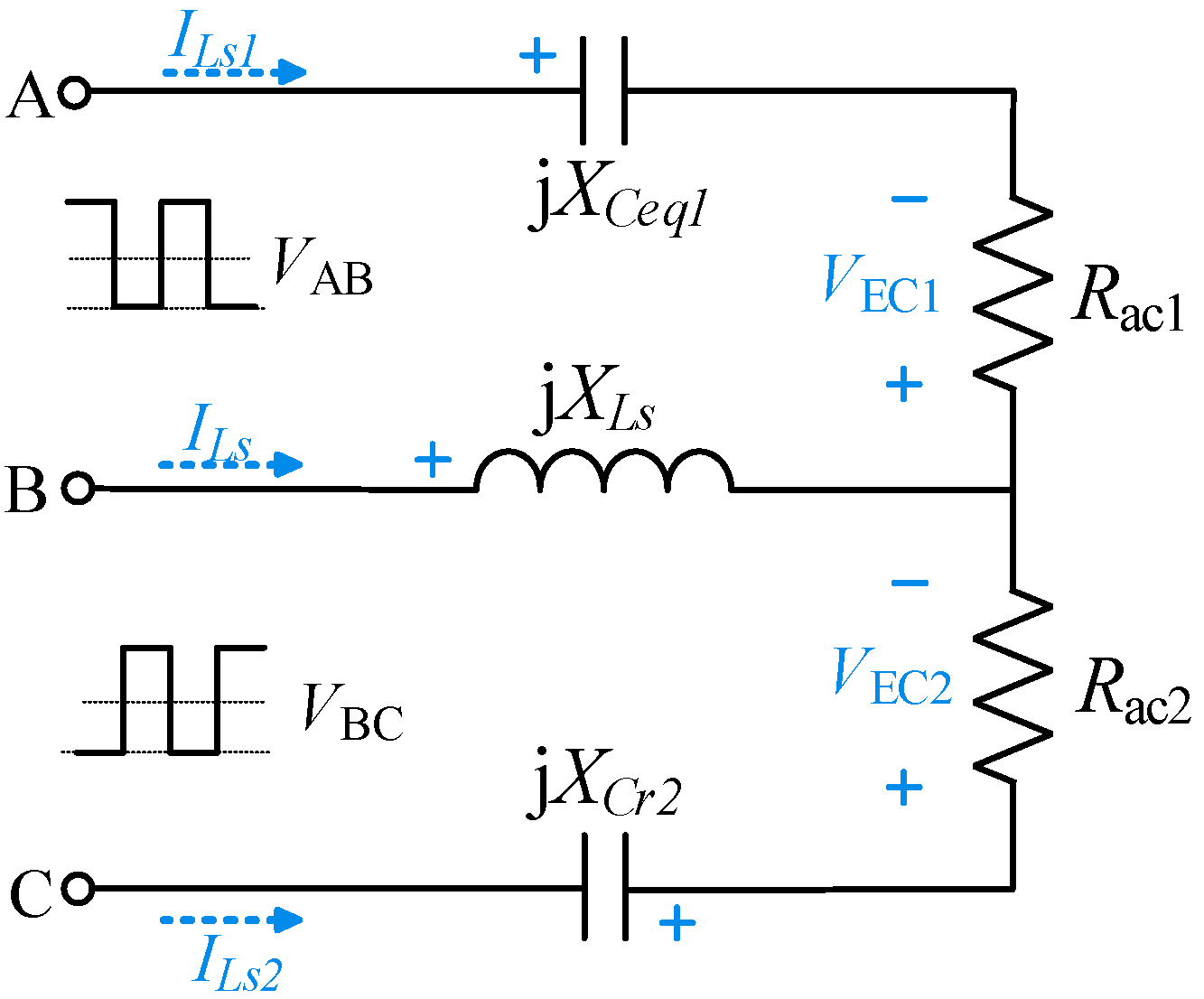
The resonant network is composed of upper and lower half-bridge switches, accompanied by resonant capacitors sharing a common inductance, denoted as LS. As a result, both resonant networks are subjected to square-wave input voltage. As depicted in Figure 4, the resonant inductance current, referred to as ILs1, flows from point A to point B, while another resonant inductance current, denoted as ILs2, flows from point C to point B.
By utilizing fixed-frequency PWM modulation, switches S1 and S2 demonstrate complementary conduction with respect to their duty cycles. Based on Fourier series analysis [16], the equivalent input voltage for each phase can be calculated as follows:
V AB = V in / 2 + 2 V in sin D t / π V BC = V in / 2 + 2 V in sin ( 1 D ) t / π
where D represents the duty cycle of switch tube S1, while VAB denotes the square-wave voltages generated by the upper bridge arms, and VBC denotes the square-wave voltages generated by the lower bridge arms.
The resonant frequencies of the two resonant networks are different, due to the varying capacitance values of the two resonant capacitors.
f r 1 = 1 2 π L s C e q 1 f r 2 = 1 2 π L s C r 2
Now, we will delve into a detailed analysis of the upper half-bridge resonant network. Upon application of the square wave VAB of the half-bridge inverter network to the resonant network comprised of LS and Cr1, it is observed that the basic components of the AC-equivalent output load voltage vec1 and current exhibit sinusoidal characteristics. Following a thorough classic AC analysis, the voltage gain of the AC equivalent circuit of the upper half-bridge resonant network can be expressed as:
V EC 1 V AB = R ac 1 sin π ( 1 D ) R ac 1 + j ( X L s X C e q 1 )
where XLS represents the common inductance reactance, XCR1 signifies the capacitance reactance of the upper half-bridge resonant network, and Rac1 denotes the AC-equivalent resistance.
X L s = 2 π f s L s X C e q 1 = 1 / 2 π f s C e q 1 R ac 1 = 8 R eq 1 / π 2
The LED parallel impedance of the first group of two current-sharing output units, Req1, is given by RLED1//RLED2. According to Equations (3) and (4), the static gain G1 of the upper half-bridge resonant network is:
G 1 = V LED 1 + V LED 2 V in = ( π + 4 sin π D ) sin ( π D ) 2 π 1 + ( X L s X C r 1 R ac 1 ) 2
The static gain G2 of the lower half-bridge resonant network is similarly defined and can be expressed as follows:
G 2 = V LED 3 + V LED 4 V i n = ( π 4 sin π ( 1 D ) sin π ( 1 D ) 2 π 1 + ( X Ls X C r 2 R ac 2 ) 2
where the capacitance reactance XCr2 and the AC-equivalent resistance Rac2 of the lower half-bridge resonant network are determined by the following equations:
X c r 2 = 1 / 2 π f s C r 2 R ac 2 = 8 R eq 2 / π 2
Additionally, Req2 represents the LED parallel impedance of the second group of two current-sharing output units, with a specific value denoted as RLED3//RLED4.

3.2. Constant-Frequency PWM Dimming

The integrated half-bridge switched resonant unit comprises switches S1 and S2, the common inductance LS, resonant capacitors Cr1 and Cr2, and the controllable switched capacitor unit, which includes switch S3 and switched capacitor CS1. Utilizing the complementary conduction of switches S1 and S2 and a fixed switching frequency, this study implements constant-frequency PWM to regulate the output currents of the four LEDs. Equation (2) indicates that the LED driver possesses two distinct resonant frequencies. Upon meticulous analysis, the switching frequency fs of the driver is selected to be near the maximum resonant frequency, and the output current is adjusted by modifying the duty cycle D of switch S1. The relationship between load currents ILED1/2 and ILED3/4 and duty cycle D is depicted in Figure 5, based on the PSIM 9.1.4 simulation. The maximum load current occurs at D = 0.4. Specifically, the load current ILED1/2 can continuously vary from 219 mA to 392 mA, while the load current ILED3/4 can continuously shift from 118 mA to 219 mA. The discussion proceeds to explore the LED load current of the upper and lower current-sharing output units. By referencing the equivalent circuit diagram in Figure 4, the branch current ratio K is taken into account.
K = I LED 1 / 2 I LED 3 / 4 = R ac 1 + j ( X L s X C e q 1 ) R ac 2 + j ( X L s X C r 2 ) = R ac 1 2 + ( X L s X C e q 1 ) 2 R ac 2 2 + ( X L s X C r 2 ) 2
In this study, the branch current ratio K can be adjusted by choosing different capacitance values, subsequently affecting the average current in any branch of the first two-way current-sharing output unit (ILED1/2) and the second two-way current-sharing output unit (ILED3/4). The current values of the two LED current-sharing output units change proportionally by modifying the equivalent capacitance value of the controllable switched capacitor unit. It is essential to highlight that the amount of charge in a switching cycle is directly proportional to the capacitance. As a result, the capacitance change value, Csv1, when adjusting the controllable switched capacitor unit plays a critical role in determining the overall current distribution.
C s v 1 = Δ Q cs 1 Q cs 1 = 1 cos 2 π D δ / 180 2 C s 1
The equivalent capacitance Ceq1 of the controllable switched capacitor unit can be ascertained using the following formula, where qcs1 symbolizes the charge amount corresponding to capacitor CS1, and D signifies the duty cycle of switch tube S3 within the unit. Assuming Cb1 maintains a constant value, the angle of the voltage VAB phase, denoted by θ, precedes the output current ILS angle in this context.
C e q 1 = C b 1 + C s v 1 = C b 1 + 1 cos 2 π D δ / 180 2 C s 1
The aforementioned formula demonstrates that the controllable switched capacitor unit possesses an equivalent capacitance range of [Cb1, Cs1 + Cb1], with the maximum duty cycle D not surpassing 0.9. In the steady state, the current is filtered by the rectifier diode and output capacitor according to the driver’s operating mode. Further analysis establishes the correlation between the output current and the absolute value Im of the resonant inductance peak, as follows:
I LED 1 + I LED 3 = 2 I m 1 + I m 2 π
The switching loss is calculated as follows:
P sw = f b ( E on ( I on , T ) + E off ( I off , T ) )
Among them, Eon (Ion, T) is the turn-on loss energy corresponding to the current of a single turn-on process in the positive half-cycle of the chopping of the semiconductor switching device, which is obtained by quadratic interpolation of the junction temperature T and the conduction current Ion; Eoff(Ioff, T) is the turn-off loss energy corresponding to the current of a single turn-off process in the positive half-cycle of the chopping of the semiconductor switching device, which is obtained by quadratic interpolation of the junction temperature T and the turn-off current Ioff; Eon(Ion, T) and Eoff(Ioff, T) are added, respectively, to obtain the switching loss in a single fundamental period, and switching loss is multiplied in a single fundamental period by the fundamental frequency fb to obtain the chopper switching loss Psw.

4. Performance Analysis of LED Driver

4.1. Current-Sharing Characteristics among Output Branches

Based on the modal analysis, modes 2 and 6 show that the unidirectional conductivity of the diodes leads to the controllable switched capacitor unit discharging through load LED1 and freewheeling diodes D2 and D4. Within each switching cycle, the quantity of charge stored by the controllable switched capacitor unit, ΔQ1ch, is equivalent to the charge flowing through load LED1. In a similar manner, modes 1 and 4 reveal that the controllable switched capacitor unit discharges through load LED2 and freewheeling diodes D1 and D3. In this scenario, the amount of charge discharged by the controllable switched capacitor unit during a switching cycle, ΔQ1dis, equals the charge flowing through load LED2. Owing to the ample filter capacitance, the output current can be considered constant, resulting in the following relationship:
I LED 1 = Δ Q 1 ch / T I LED 2 = Δ Q 1 dis / T
The switching cycle, denoted as t, involves the charge amount, ΔQ1ch, ΔQ1dis, of the controllable switched capacitor unit throughout the entire cycle. Additionally, Equation (13) results from the modal analysis of modes 2 and 6, and modes 1 and 4 will not be reiterated here.
I LED 3 = Δ Q 2 ch / T I LED 4 = Δ Q 2 dis / T
The amount of charge flowing through the capacitors during the entire switching cycle can be determined using the average currents of LED3 and LED4, denoted as ILED3 and ILED4, respectively, along with the charge amount of the resonant capacitor Cr2Q2ch, ΔQ2dis). Figure 2 illustrates the charging and discharging processes of the controllable switched capacitor unit and resonant capacitor Cr2 under different modes. Based on the charge balance principle of the capacitor, the relationship between the charge amounts during the whole switching cycle is established.
Δ Q 1 dis = t 1 t 4 i C eq 1 d t = Δ Q 1 ch = t 0 t 1 i C eq 1 d t + t 4 t 6 i C eq 1 d t Δ Q 2 dis = t 1 t 4 i C r 2 d t = Δ Q 2 ch = ( t 0 t 1 i C r 2 d t + t 4 t 6 i C r 2 d t )
From Equations (13)~(15), it is evident that:
I LED 1 = I LED 2 I LED 3 = I LED 4
Therefore, the circuit topology can use the charge balance principle of the capacitor to realize the current sharing of two groups of current-sharing output units with four output currents.

4.2. Realization of Soft-Switching Conditions

To analyze the conditions for achieving zero-voltage switching with two switches, we first consider the current flowing through S1 and S2.
i s 1 = i L s ( t ) , 0 t < D T 0 , D T t < T
i s 2 = 0 , 0 t < D T i L s ( t ) , D T t < T
The condition for soft switching depends on the current flowing through the switch tube. After analysis, the instantaneous value of the resonant inductance current through the upper half-bridge resonant network at any time is:
i L s 1 ( t ) = I m 1 sin ( w s 1 t α 1 β 1 ) I m 1 = π + 4 sin π ( 1 D ) V in Z in 1
where Zin1 is the input impedance of the first group of current-sharing units.
α 1 = tan 1 ( X L s X C e q 1 R ac 1 ) β 1 = tan 1 sin 2 π ( 1 D ) 1 cos 2 π ( 1 D ) Z i n 1 = R a c 1 + j ( X L s X c e q 1 )
Similarly, the instantaneous value of the resonant inductance current flowing through the lower half-bridge resonant network at any time is:
i Ls 2 ( t ) = I m 2 sin ( W s 2 t α 2 β 2 ) I m 2 = π 4 sin π D V i n Z in 2
where Zin2 is the input impedance of the first group of current-sharing units.
α 2 = tan 1 ( X L s X c r 2 R a c 2 ) β 2 = tan 1 sin 2 π D 1 cos 2 π D Z i n 2 = R a c 2 + j ( X L s X c r 2 )
In the steady-state analysis of the converter, the appropriate choice of the switching frequency fs for the half-bridge inverter network is vital to ensure that the resonant inductance current ILS operates in continuous conduction mode (CCM) and achieves zero-voltage switching (ZVS) for both switches [17]. As depicted in Figure 2, the resonant inductor current ILS peaks at t3 and t6. At this point, the energy stored in the common inductor must be adequate to completely charge and discharge the junction capacitors of switches S1, S2, and S3. Consequently, the ZVS opening conditions for all three switches are established.
( C oss 1 + C o s s 2 + C o s s 3 ) V in 2 < 1 2 L s I L s 2 ( t 3 ) ( C oss 1 + C o s s 2 + C o s s 3 ) V in 2 < 1 2 L s I L s 2 ( t 6 )
Coss1, Coss2, and Coss3 represent the junction capacitances of switches S1, S2, and S3.

5. Simulation Analysis and Experimental Verification

5.1. Simulation Analysis

To validate the dual-channel current-sharing features and dimming control strategy of the proposed circuit topology, this study employed PSIM to build a simulation model. The simulation incorporated various impedance values for LED models to determine the current-sharing characteristics under extreme asymmetric loads. The circuit parameters used in the simulation are presented in Table 1. Figure 5 and Figure 6 display the corresponding steady-state waveforms for D = 0.15 and D = 0.4, offering a visual representation of the simulation outcomes.
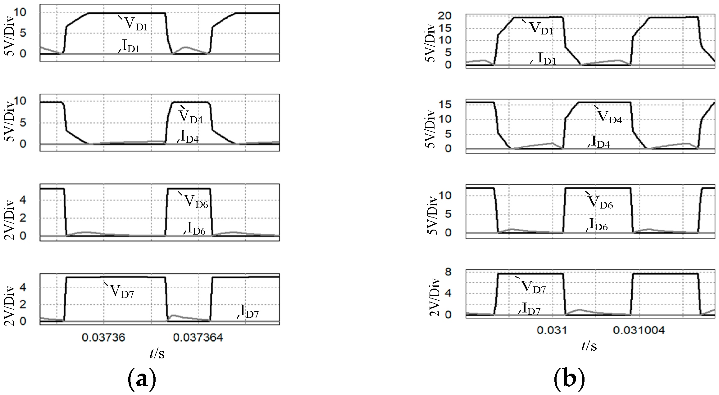
Figure 5 demonstrates that the amplitude of the steady-state load output current remains consistent for both the upper and lower current-sharing units across various impedance values. Figure 6 illustrates that the diode achieves zero-current switching (ZCS) shutdown when the current at both ends crosses zero and begins to bear the reverse voltage.

5.2. Experimental Verification

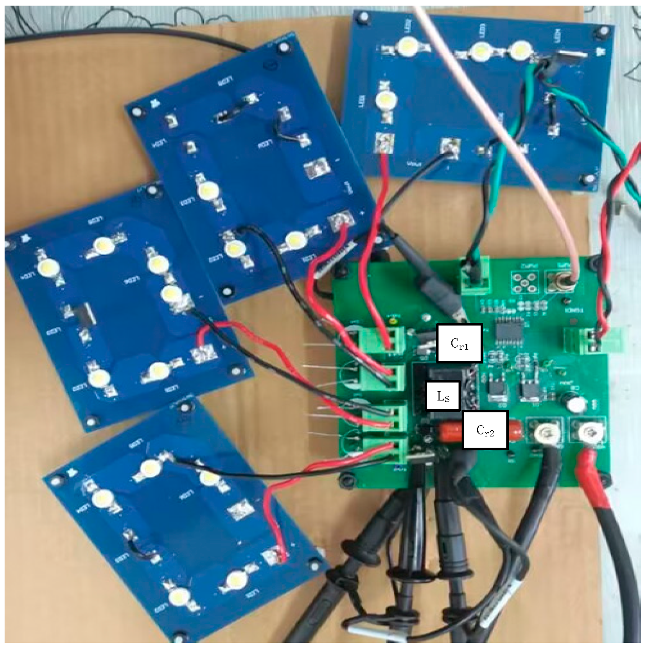
To evaluate the feasibility and performance of the proposed work mode, a 19 W experimental prototype was built. The experimental setup employed 3 W LED and included two load cases. In load case 1, the driver operated under rated load, with each of the output loads LED1, LED2, LED3, and LED4 consisting of 5, 5, 3, and 3 lamp beads, respectively. Furthermore, load case 2 was designed to assess extreme unbalanced load, with the number of lamp beads for each output load adjusted to 5, 4, 4, and 2 for LED1, LED2, LED3, and LED4, respectively. Figure 7 is one picture with the experimental test.
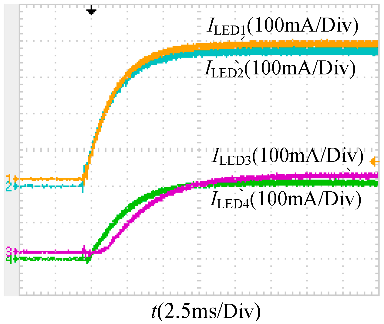
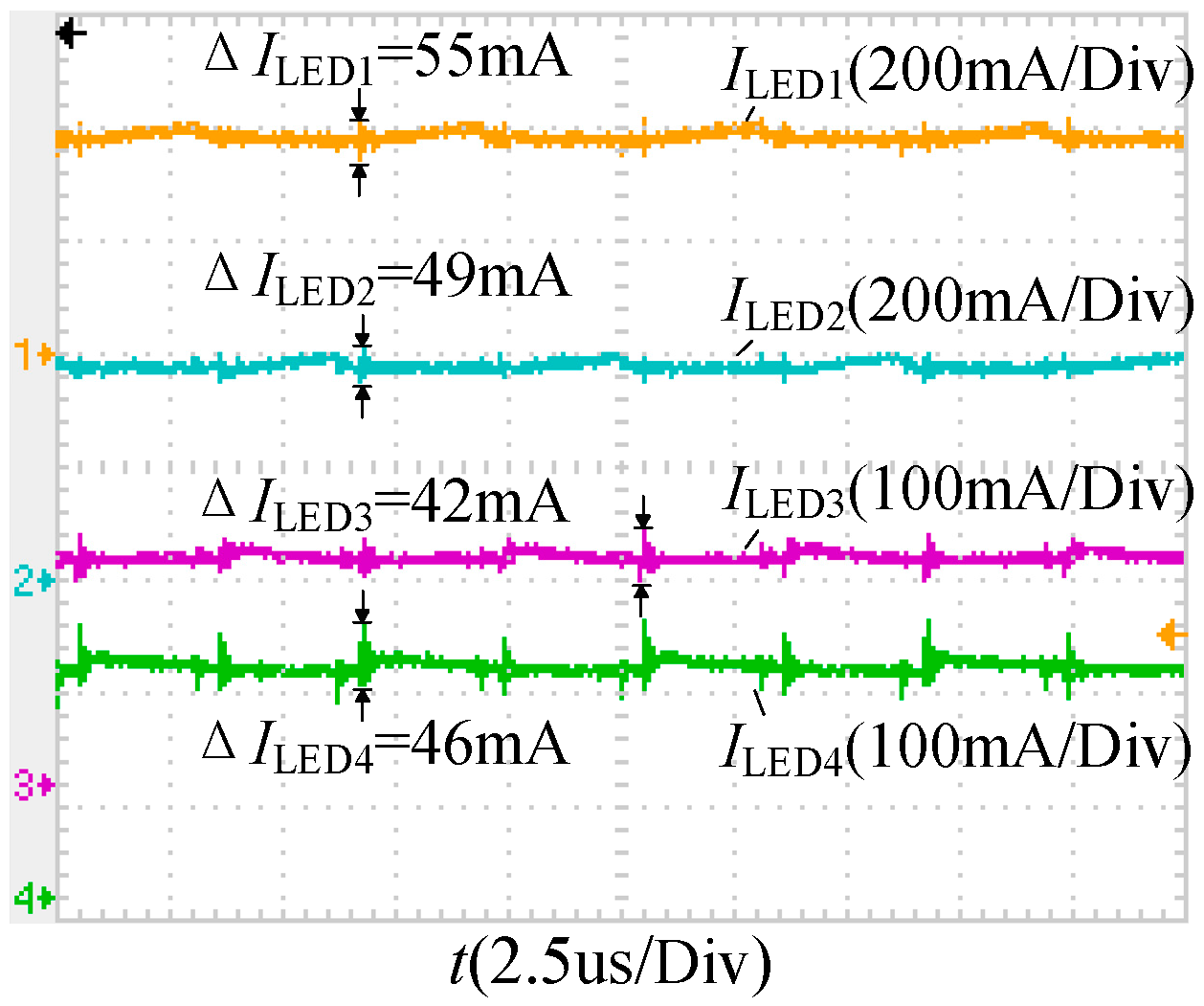
The starting process of output current under load condition 2 when D = 0.4 is illustrated in Figure 8. It is noteworthy that the starting time is less than 15 ms, and there is no overshoot. Additionally, Figure 9 displays the ripple waveform of the output current under asymmetric load with a duty cycle D of 0.4. Importantly, the current amplitudes of load currents ILED1 and ILED2 remain stable at 384 mA and 380 mA, respectively. Similarly, the current amplitude of load current ILED3 is stable at 210 mA, and that of load current ILED4 is stable at 214 mA.
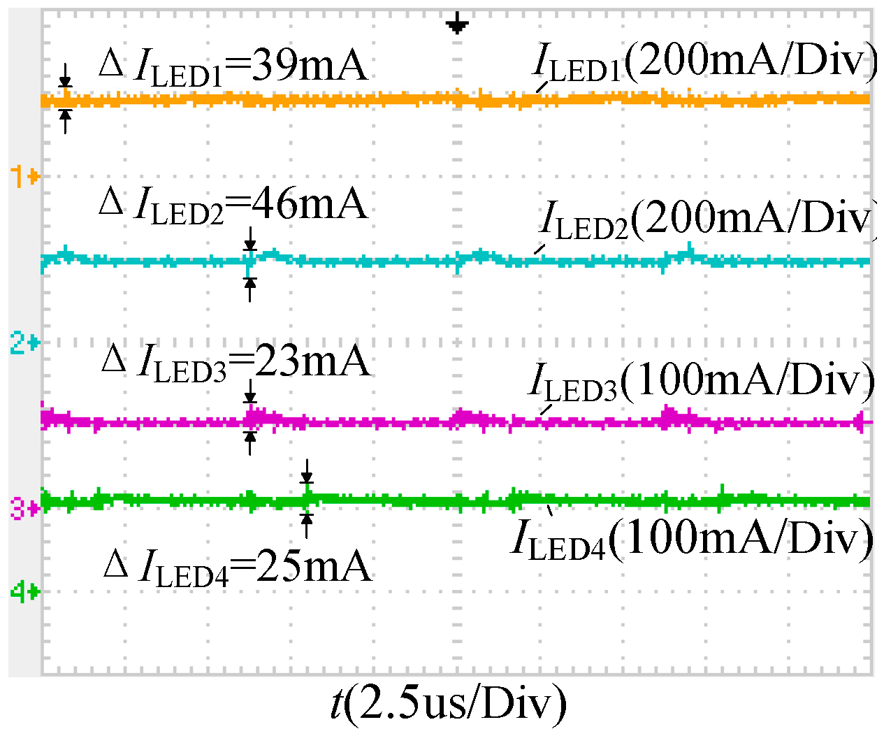
At a duty cycle of 0.15, Figure 10 demonstrates the ripple waveform of the four output currents under rated load conditions. The stable current amplitudes for load currents ILED1 and ILED2 are 188 mA and 198 mA, respectively. In addition, load currents ILED3 and ILED4 exhibit stable current amplitudes of 104 mA and 108 mA, respectively.
The experimental results indicate that the fixed dimming ratio of the two current-sharing output units is approximately 1.9:1, and despite some fluctuation, the output current maintains a high quality. In the context of luminous flux and LED service life, it is crucial to ensure that the LED’s current ripple is less than 30% to prevent flickering [18]. Figure 10 illustrates that the maximum output current ripple of the four loads is 23.2%, thus meeting the specified ripple requirements. Furthermore, the amplitudes of the four load currents under two different load conditions align closely with the simulation results shown in Figure 5, as depicted in Figure 9 and Figure 10.
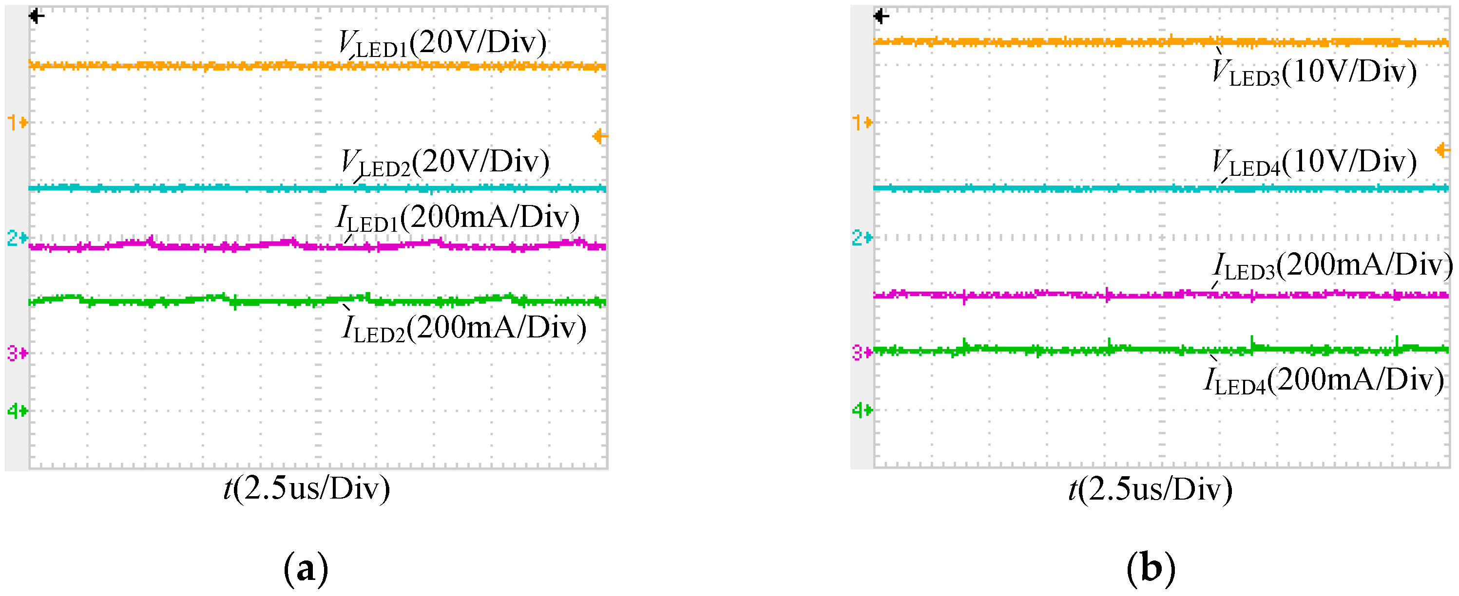
The voltage and current waveforms of two groups of current-sharing units under asymmetric load are displayed in Figure 11. Under different voltage conditions, the output load currents ILED1/2 and ILED3/4 measure 380 mA and 200 mA, respectively, as shown in the figure. The discrepancies between VLED1 and VLED2 in Figure 11a and VLED3 and VLED4 in Figure 11b are attributed to the varying number of LED loads. This observation serves as evidence that the upper and lower current-sharing output units of this driver exhibit favorable current-sharing characteristics.
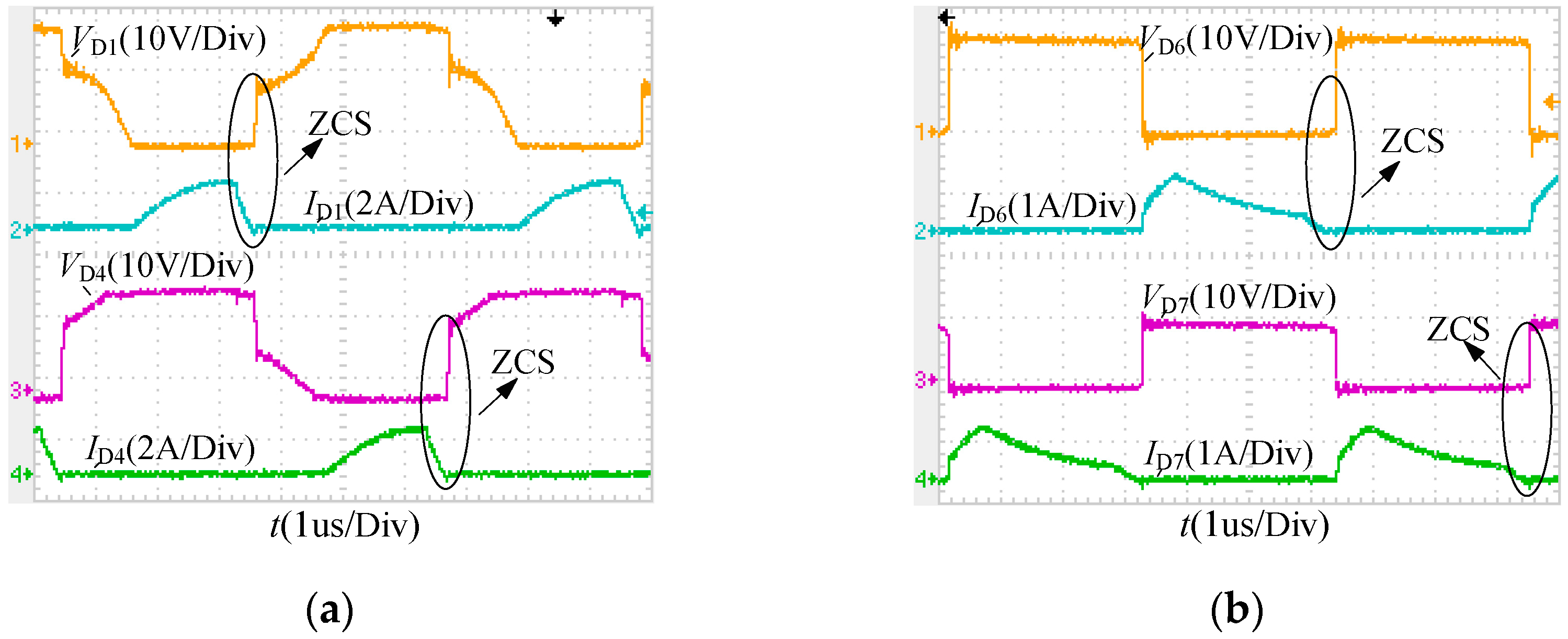
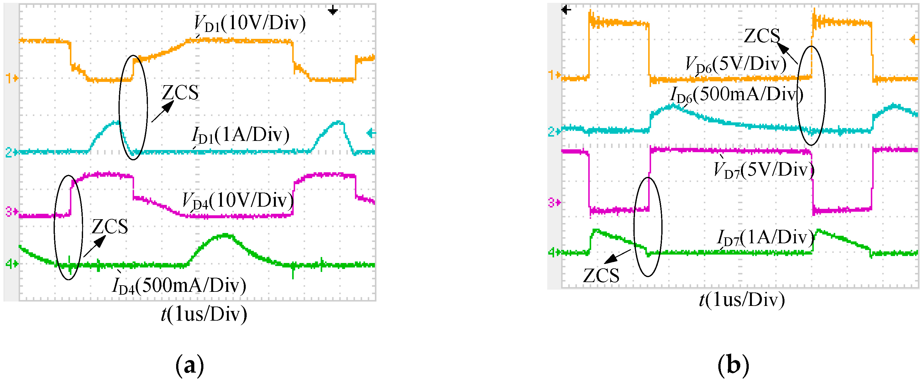
Additionally, Figure 12 presents the soft-switching waveform of the switch tube when the duty cycle D = 0.4, demonstrating that all the switch tubes can achieve ZVS opening. Furthermore, the voltage and current waveforms of diodes are detailed in Figure 13 and Figure 14 under two different load conditions, revealing that the voltage stresses of diodes D1 and D4 in Figure 13a are equivalent to the output load voltages vled1 and vled2 in Figure 11a, while the voltage stresses of diodes D6 and D7 in Figure 13b correspond to the output load voltages vled3 and vled4 in Figure 11b. This equality results in lower voltage stress for the diodes. Additionally, the constant-frequency PWM modulation process indicates that ZCS can be turned off throughout, thereby reducing the reverse recovery loss of the diode.

6. Discussion

In recent years, extensive research has been conducted on multi-channel dimming LED drivers. This study provides a comparison of the number of components, soft-switching capability, output load, and efficiency of these drivers, both domestically and internationally, as shown in Table 2. Notably, the input voltage of references [6,12,15] and the LED driver in this study is 48 V. Upon comparing these parameters, it becomes evident that the LED driver proposed in this paper has fewer switching devices and can accommodate more output loads. As a result, the entire system boasts a higher power density and has the capability to adjust the output current in proportion to the upper and lower current-sharing output units, offering superior soft-switching conditions and overall high efficiency. The efficiency curve obtained from experimental tests conducted on the proposed LED driver is presented in Figure 15, specifically when the current of the first two-way current-sharing output unit falls within the range of 188 mA to 400 mA. Notably, the efficiency is observed to peak at 380 mA, reaching an impressive 96.56%. This finding underscores the high efficiency and robust performance of the LED driver under varying loads, as demonstrated in the experimental results.

7. Conclusions

This paper presents a resonant soft-switching four-way LED output driver designed for multi-color lighting applications. The driver’s capability for proportional dimming of two sets of current-sharing output units using only three switches and one inductor is demonstrated through theoretical analysis and experimental prototype verification. The amplitude of the output current can be proportionally adjusted under constant-frequency PWM control by controlling the switched capacitor. Additionally, both sets of current-sharing output units exhibit effective current sharing. Throughout the operation, all switches and diodes achieve soft switching, thereby reducing switching losses and ensuring high efficiency.
In a global context, the benefits of the resonant soft-switching four-way LED output driver designed for multi-color lighting applications could include the following:
  • Energy efficiency: The driver’s ability to achieve soft switching reduces switching losses, leading to higher efficiency. This is especially valuable in a global context, where energy conservation is a major concern.
  • Versatile lighting options: The multi-color lighting application of this driver allows for greater flexibility in creating diverse lighting effects and moods, catering to different global design and aesthetic preferences.
  • Cost savings: The use of only three switches and one inductor in the design simplifies the circuit and potentially reduces manufacturing costs. This can have a positive impact on the global market, making the technology more accessible and cost-effective.

Author Contributions

Conceptualization, J.Z. and L.J.; methodology, L.J.; software, W.X.; validation, L.J. and W.X.; formal analysis, L.J. and W.X.; investigation, L.J. and W.X.; resources, L.J. and W.X.; writing—original draft preparation, W.X.; writing—review and editing, L.J. and W.X.; visualization, L.J.; supervision, L.J. All authors have read and agreed to the published version of the manuscript.

Funding

This research received no external funding.

Data Availability Statement

Data is contained within the article.

Conflicts of Interest

The authors declare no conflicts of interest.

References

  1. Castro, I.; Vazquez, A.; Lamar, D.G.; Arias, M.; Hernando, M.M.; Sebastian, J. An electrolytic capacitorless modular three-phase AC-DC LED driver based on summing the light output of each phase. IEEE J. Emerg. Sel. Top. Power Electron. 2019, 7, 2255–2270. [Google Scholar] [CrossRef]
  2. Wu, B.-S.; Mansoori, M.; Trumpler, K.; Addo, P.W.; MacPherson, S.; Lefsrud, M. Effect of Amber (595 nm) Light Supplemented with Narrow Blue (430 nm) Light on Tomato Biomass. Plants 2023, 12, 2457. [Google Scholar] [CrossRef] [PubMed]
  3. Guan, H.; Ji, Q.; Han, T.; Cheng, M. Research on DC distribution mode of LED lighting system in plant factory. Electron. World 2022, 25–27. [Google Scholar] [CrossRef]
  4. Nacheva, L.; Dimitrova, N.; Koleva-Valkova, L.; Stefanova, M.; Ganeva, T.; Nesheva, M.; Tarakanov, I.; Vassilev, A. In Vitro Multiplication and Rooting of Plum Rootstock ‘Saint Julien’ (Prunus domestica subsp. insititia) under Fluorescent Light and Different LED Spectra. Plants 2023, 12, 2125. [Google Scholar] [CrossRef] [PubMed]
  5. Chen, H.; Zhang, Y.; Ma, D. A SIMO Parallel-String Driver IC for Dimmable LED Backlighting with Local Bus Voltage Optimization and Single Time-Shared Regulation Loop. IEEE Trans. Power Electron. 2012, 27, 452–462. [Google Scholar] [CrossRef]
  6. Dong, Z.; Chi, K.T.; Hui, S.R. Current-Source-Mode Single-Inductor Multiple-Output LED Driver with Single Closed-Loop Control Achieving Independent Dimming Function. IEEE J. Emerg. Sel. Top. Power Electron. 2018, 6, 1198–1209. [Google Scholar] [CrossRef]
  7. Reddy, U.R.; Narasimharaju, B.L. Cost-Effective Zero-Voltage Switching Dual-Output LED Driver. IEEE Trans. Power Electron. 2017, 32, 7941–7953. [Google Scholar] [CrossRef]
  8. Veeramallu, V.K.S.; Porpandiselvi, S.; Narasimharaju, B.L. A buck-boost integrated high gain non-isolated half-bridge seriesresonant converter for solar PV/battery fed multiple load LED lighting applications. Int. J. Circuit Theory Appl. 2020, 48, 266–285. [Google Scholar] [CrossRef]
  9. Veeramallu, V.K.S.; Porpandiselvi, S.; Narasimharaju, B.L. A Nonisolated Wide Input Series Resonant Converter for Automotive LED Lighting System. IEEE Trans. Power Electron. 2021, 36, 5686–5699. [Google Scholar] [CrossRef]
  10. Molavi, N.; Farzanehfard, H. Load-Independent Hybrid Resonant Converter for Automotive LED Driver Applications. IEEE Trans. Power Electron. 2022, 37, 8199–8206. [Google Scholar] [CrossRef]
  11. Molavi, N.; Farzanehfard, H. A Nonisolated Wide-Range Resonant Converter for LED Driver Applications. IEEE Trans. Ind. Electron. 2023, 70, 8939–8946. [Google Scholar] [CrossRef]
  12. Tian, H.; Liu, J.; Zeng, J. Constant frequency resonant multi-channel LED current sharing driver based on controllable switched capacitor. Acta Electrotech. Sin. 2019, 34, 286–295. [Google Scholar]
  13. Liang, G.; Tian, H.; An, Z.; Zhang, T.; Zhang, X. A new multi-channel independent dimming LED driver. New Technol. Electr. Energy 2020, 39, 72–80. [Google Scholar]
  14. Yada, T.; Katamoto, Y.; Yamada, H.; Tanaka, T.; Okamoto, M.; Hanamoto, T. Design and Experimental Verification of 400-W Class LED Driver with Cooperative Control Method for Two-Parallel Connected DC/DC Converters. Energies 2018, 11, 2237. [Google Scholar] [CrossRef]
  15. Kolla, H.R.; Vishwanathan, N.; Murthy, B.K. Independently Controllable Dual-Output Half-Bridge Series Resonant Converter for LED Driver Application. IEEE J. Emerg. Sel. Top. Power Electron. 2022, 10, 2178–2189. [Google Scholar] [CrossRef]
  16. Wang, H.; Chen, Y.; Liu, Y.F.; Yang, Z.A.; Afsharian, J.; Gong, B. LLC resonant converter with shared power switches and dual coupled resonant tanks to achieve automatic current sharing. In Proceedings of the 2017 IEEE Energy Conversion Congress and Exposition (ECCE), Cincinnati, OH, USA, 1–5 October 2017; pp. 5712–5719. [Google Scholar]
  17. Martins, M.; Perdigao, M.S.; Mendes, A.M.; Pinto, R.A.; Alonso, J.M. Analysis, Design, and Experimentation of a Dimmable Resonant-Switched-Capacitor LED Driver With Variable Inductor Control. IEEE Trans. Power Electron. 2017, 32, 3051–3062. [Google Scholar] [CrossRef]
  18. Yu, Y.; Zhang, F.; Ni, J. Symmetrical jumper capacitor LED current sharing circuit. J. Electrotech. 2014, 29, 196–203. [Google Scholar]
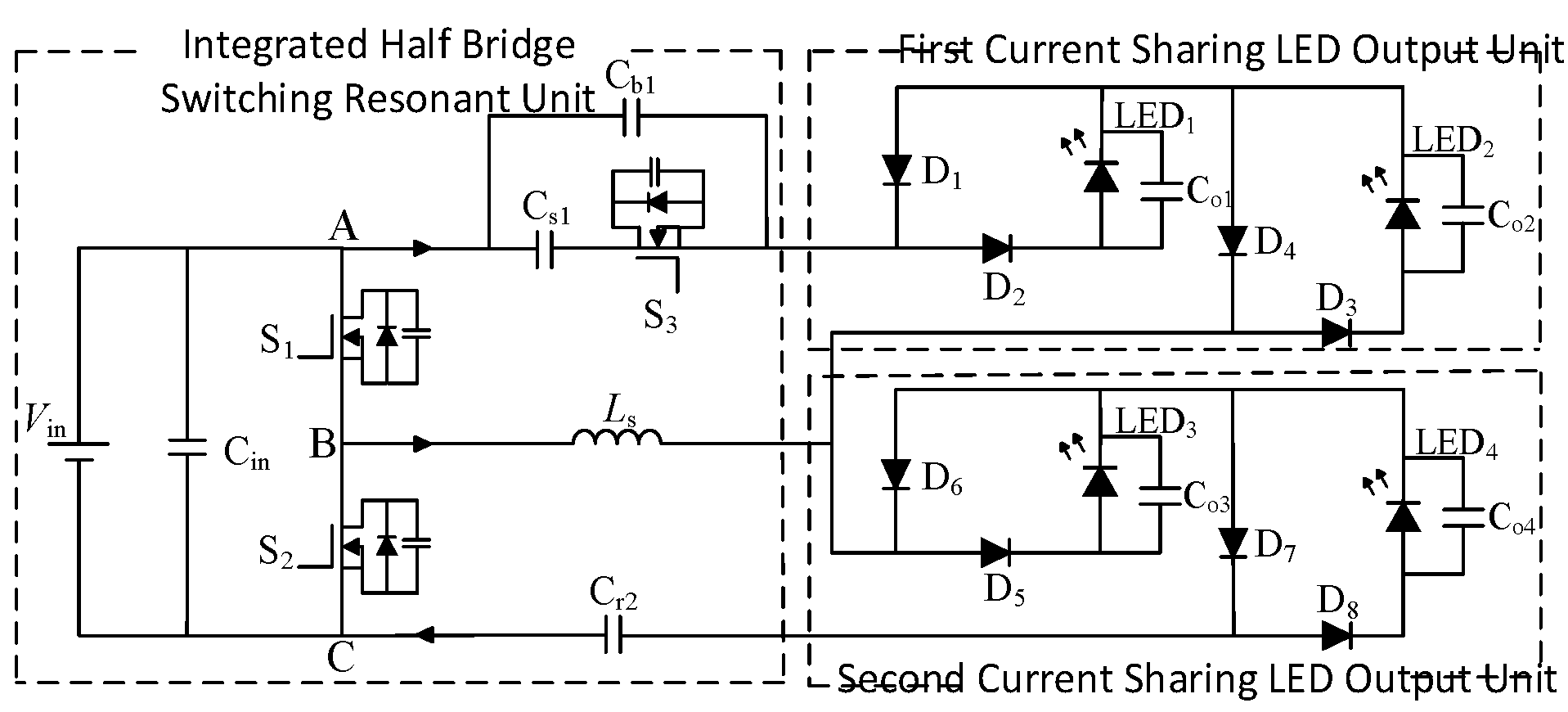
Figure 1. Proposed LED driver circuit diagram.
Energies 17 01368 g001
Figure 2. Proposed converter’s key waveforms.
Energies 17 01368 g002
Figure 3. Proposed working modes of the converter: (a) Mode 1; (b) Mode 2; (c) Mode 3; (d) Mode 4; (e) Mode 5; (f) Mode 6.
Energies 17 01368 g003
Figure 4. Equivalent circuit of the double-resonant network.
Energies 17 01368 g004
Figure 5. Four load output current simulation waveforms: (a) D = 0.15; (b) D = 0.4.
Energies 17 01368 g005
Figure 6. Simulation waveform of diode soft switching. (a) D = 0.15; (b) D = 0.4.
Energies 17 01368 g006
Figure 7. One picture with the experimental test.
Energies 17 01368 g007
Figure 8. D = 0.4, output current startup waveform.
Energies 17 01368 g008
Figure 9. D = 0.4, output current ripple at load 2.
Energies 17 01368 g009
Figure 10. D = 0.15; output current ripple at load 1.
Energies 17 01368 g010
Figure 11. D = 0.4, output waveform at load 2. (a) The current-sharing unit in Group I. (b) The second set of units sharing currents.
Energies 17 01368 g011
Figure 12. Switch tubes S1 and S2 produce a soft-switching waveform.
Energies 17 01368 g012
Figure 13. D = 0.4, diode soft-switching waveform under load 2. (a) Voltage and current waveforms of diodes D1 and D4. (b) Voltage and current waveforms of diodes D6 and D7.
Energies 17 01368 g013
Figure 14. D = 0.15, diode soft-switching waveform under load 1. (a) Voltage and current waveforms of diodes D1 and D4. (b) Voltage and current waveforms of diodes D6 and D7.
Energies 17 01368 g014
Figure 15. Output current efficiency curve.
Energies 17 01368 g015
Table 1. Parameters and model of the LED driver.
NameValue or Model
Input voltage (Vin)48 V
Common inductance (Ls)10 uH
Resonant capacitance (Cs1/Cr2/Cb1)100 nF/68 nF/68 nF
Switching frequency (fs)112 kHz
Filter capacitor (Co1~Co4)10 uF
Load10 Ω
Switching (S1,S2,S3)NCE0224K
Diode (D1~D8)ES5DB
Table 2. LED driver comparison.
Number of Switch TubesNumber of Inductance Number of CapacitanceNumber of Load ZVSZCSMaximum Efficiency
Literature [4]3122nono88%
Literature [5]2132yesno95.5%
Literature [7]4231yesno94.19%
Literature [9]3231yesyes97.8%
Literature [10]31104yesno94.1%
Literature [12]3262yesno91.5%
this paper3174yesyes96.56%
Disclaimer/Publisher’s Note: The statements, opinions and data contained in all publications are solely those of the individual author(s) and contributor(s) and not of MDPI and/or the editor(s). MDPI and/or the editor(s) disclaim responsibility for any injury to people or property resulting from any ideas, methods, instructions or products referred to in the content.