Article

Two Types of Asymmetric Switched-Capacitor Five-Level Single-Phase DC-AC Inverters for Renewable Energy Applications

1
Department of Electrical Engineering, Feng Chia University, No. 100, Wenhwa Road, Seatwen, Taichung 40724, Taiwan
2
Department of Electrical Engineering, National Taipei University of Technology, 1, Sec. 3, Zhongxiao E. Rd., Taipei 10608, Taiwan
*
Author to whom correspondence should be addressed.
Energies 2024, 17(5), 983; https://doi.org/10.3390/en17050983
Submission received: 8 January 2024 / Revised: 9 February 2024 / Accepted: 17 February 2024 / Published: 20 February 2024
(This article belongs to the Section A: Sustainable Energy)

Abstract

:
Two types of asymmetric switched-capacitor five-level single-phase DC-AC inverters are presented based on the clamping half-bridge circuit and the output half-bridge circuit. Furthermore, the switches of the two proposed circuits can be driven by half-bridge gate drivers and can be modularized. Moreover, the detailed analysis of the operation principle, design of clamping capacitor and output filter of these two inverters are presented. Finally, the feasibility and validity of the proposed structures are verified by PSIM-simulated results and experimental results using FPGA as the control kernel, respectively.

1. Introduction

1.1. Motivations

Renewable energy sources, including solar [1,2], wind [3,4], hydro [5,6], geothermal [7,8], tidal [9,10], biomass [11,12], and hydrogen [13,14], are considered to be environmentally friendly because they are continuous, sustainable, and do not emit harmful emissions. In recent years, global awareness of environmental protection has increased, and more and more renewable energy sources have been encouraged to be integrated into the power grid for power generation or energy storage systems [15,16,17,18,19].
Renewable energy can facilitate decentralization of energy and electricity and enhance the security and reliability of energy supply [2,3,17,18,19]. However, the development of renewable energy still faces a number of challenges, such as energy storage and transmission technologies, energy policies and market uncertainties, and so on [20]. Consequently, in the process of facilitating the development of renewable energy, it is necessary to strengthen technological research and market development, and actively formulate and implement policies and regulations favorable to the development of renewable energy. However, harmonics content in voltage and/or current wave will cause distortions and make it non-sinusoidal. Hence, it is needed to reduce harmonics so as to improve the total harmonic distortion (THD) and efficiency of the system.
The American Institute of Electrical and Electronics Engineers (IEEE) develops the IEEE 1547 standard [21], which is an interconnection standard for distributed energy resources, including solar photovoltaic systems, wind turbines, fuel cells, etc. The standard contains many aspects, including many requirements such as AC power control, frequency and voltage control, protection and safety, fault and failure mode management, etc. The IEEE 519 standard [22] is proposed to protect the equipment in the power system from the adverse effects of harmonics, and to protect the harmonic content in the system from exceeding the safe and acceptable limits. In addition, recommendations are provided on the limitation and control of harmonic voltages and currents in power systems. In Europe, the International Electrotechnical Commission (IEC) has issued the IEC 60038 standard [23], which defines the range of voltages and frequencies to be supplied to power systems used at fixed frequencies to ensure compatibility between different electrical equipment and stability and reliability under different environmental conditions. At the same time, a series of IEC 61000 standards has been promulgated under the title of Electromagnetic Compatibility (EMC), belonging to the IEC 61000-3-X part, which covers output and input noise limitations for electrical and electronic equipment in power systems, including limitations on harmonics and abnormal voltages, etc. The IEC 61000-3-2 [24] aims to limit the effect of electrical equipment (e.g., household appliances, industrial equipment, etc.) on the harmonic currents in public low-voltage power systems, whereas the IEC 61000-3-3 [25] aims to determine the limits of the input noises of electronic equipment in low-voltage power systems in order to ensure the compatibility of the various types of electronic equipment and to minimize disturbances and damage in the power grid. In addition, the IEC 62109-1 standard [26] has been developed for the specifications of safety performance requirements for inverters in solar power systems.
Currently, the electricity provided by renewable energy can be divided into alternating current (AC) voltage from hydroelectric power and wind power through rotating motors, and direct current (DC) voltage from solar power and fuel cells through semiconductor physical and chemical energy conversion. In order to cope with the AC utility power system, AC-DC rectifiers are combined with DC-AC inverters or DC-AC inverters are used to further convert green energy into AC power. Therefore, the DC-AC inverter is one of the most important components used for power transmission.
Nowadays, DC-AC inverters are developing towards high efficiency and low harmonic components. Therefore, the development trend of multilevel inverters is towards achieving a large number of levels with a small number of power components, reducing component losses and developing multilevel inverters (MLIs). The principle of MLIs is to utilize several capacitors and power switches to change the conduction path, so as to clamp and create voltages of several levels to make the output voltage be presented on several levels.
Typical multilevel inverters include the neutral point clamped (NPC) inverter, the flying capacitor (FC) inverter, and the cascaded H-bridge (CHB) inverter [27]. In terms of the circuit structure, it can be further categorized into symmetric MLIs and asymmetric MLIs [28]. Although symmetric MLIs have the advantages of simple control and modular replacement over asymmetric MLIs, they use more power-switching components than asymmetric MLIs, thereby leading to higher costs and larger size and weight. On the other hand, the more levels there are, the more the output voltage can be reduced without the need for external inductors or filters to decrease the harmonic components of the output waveform, and the output voltage can be close to the sinusoidal waveform. In addition, the voltages across some power switches can be clamped by the level voltages to reduce the switch voltage stresses and improve the overall conversion efficiency [27,28]. Based on the foregoing reasons, the five-level DC-AC inverter is rather popular in practice applications.

1.2. Statement of the Related Works

Figure 1 shows typical five-level asymmetric inverters, including the diode neutral-point-clamped inverter [29], the T-type neutral-point-clamped inverter [30], and the flywheel capacitor inverter [31]. The main half-bridge circuit is operated based on the positive and negative half-cycles of the output voltage, and the multilevel inverter achieves the unipolar PWM-switching strategy by using control force alignment compensation. Since the switched-capacitor circuit consists of one or more capacitors and one or more power switches and is often used to maintain the voltages across the capacitors at several times the input DC voltage, the output voltage of the circuit is controlled by switching the capacitors to charge and discharge through the active components to achieve the output voltage at a relatively high number of voltage levels [32,33].
There are many other existing papers presented on the asymmetric five-level single-phase DC-AC inverters [2,34,35,36,37,38,39,40,41,42,43,44,45,46,47,48,49,50] with voltage gain and circuit structure considered, to be summarized in Table 1.

1.3. Contributions

In this paper, two types of asymmetric switched-capacitor five-level single-phase DC-AC inverters are presented based on the clamping half-bridge circuit and the output half-bridge circuit. Furthermore, the switches of the two proposed circuits can be driven by half-bridge gate drivers and can be modularized. Not only can the sinusoidal output voltage with high efficiency and low harmonic distribution (THD) be obtained for the AC power source, but also analysis can be carried out on the operation principle, clamping capacitor, and output filter design of these two inverters in detail. In addition, the feasibility and effectiveness of the proposed structures are demonstrated by PSIM simulation software (9.11 version), and an FPGA chip is used as a digital control kernel to implement the inverters to stabilize the sinusoidal output voltages.
The contents of the paper are outlined as follows. Section 2 illustrates the proposed MLI, including circuit descriptions, switching patterns, and operating principles. Section 3 describes how to design power components. Section 4 displays simulated and experimental results along with discussions. Finally, Section 5 makes some conclusions.

2. Operating Principles of the Proposed Inverters

The proposed two types of asymmetric capacitor-switched five-level DC-AC inverters are constructed and shown in Figure 2 and Figure 3. From these two circuits, the output of the half-bridge circuit, connected to the load, is called an output half bridge; similarly, the double-voltage clamping circuit is composed of a half-bridge circuit, diodes, capacitors, and power switches, and accordingly the function of this half-bridge circuit is called a clamping half bridge.

2.1. Symbol Definitions and Circuit Assumptions

Prior to analyzing the operating principles of the proposed circuits, the associated symbols and required assumptions are given:
(1)
Vin is the input voltage, vo is the output voltage, N is the reference point of zero potential, and Ro is the output resistance;
(2)
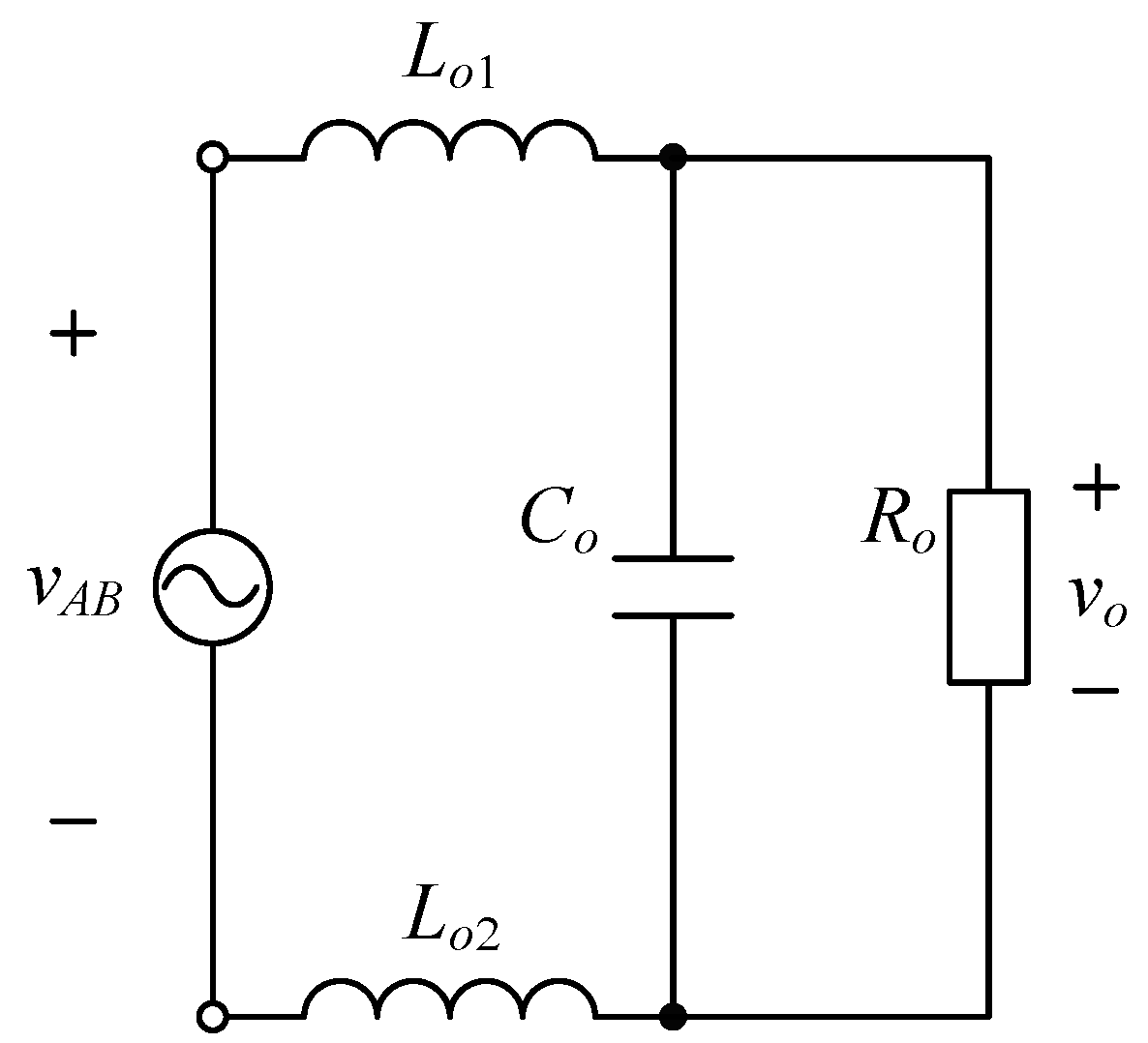
Lo1 and Lo2 are filter inductors, Co is a filter capacitor, and C1 to C4 are clamping capacitors;
(3)
iL is the current flowing through inductors Lo1 and Lo2, iCo is the current flowing through capacitor Co, and io is the output current;
(4)
S1 to S8 are switches and D1 to D4 are diodes;
(5)
Assuming that the values of the clamping capacitors are large enough, the voltages across them can be reviewed as constant values;
(6)
All components are assumed to be ideal.

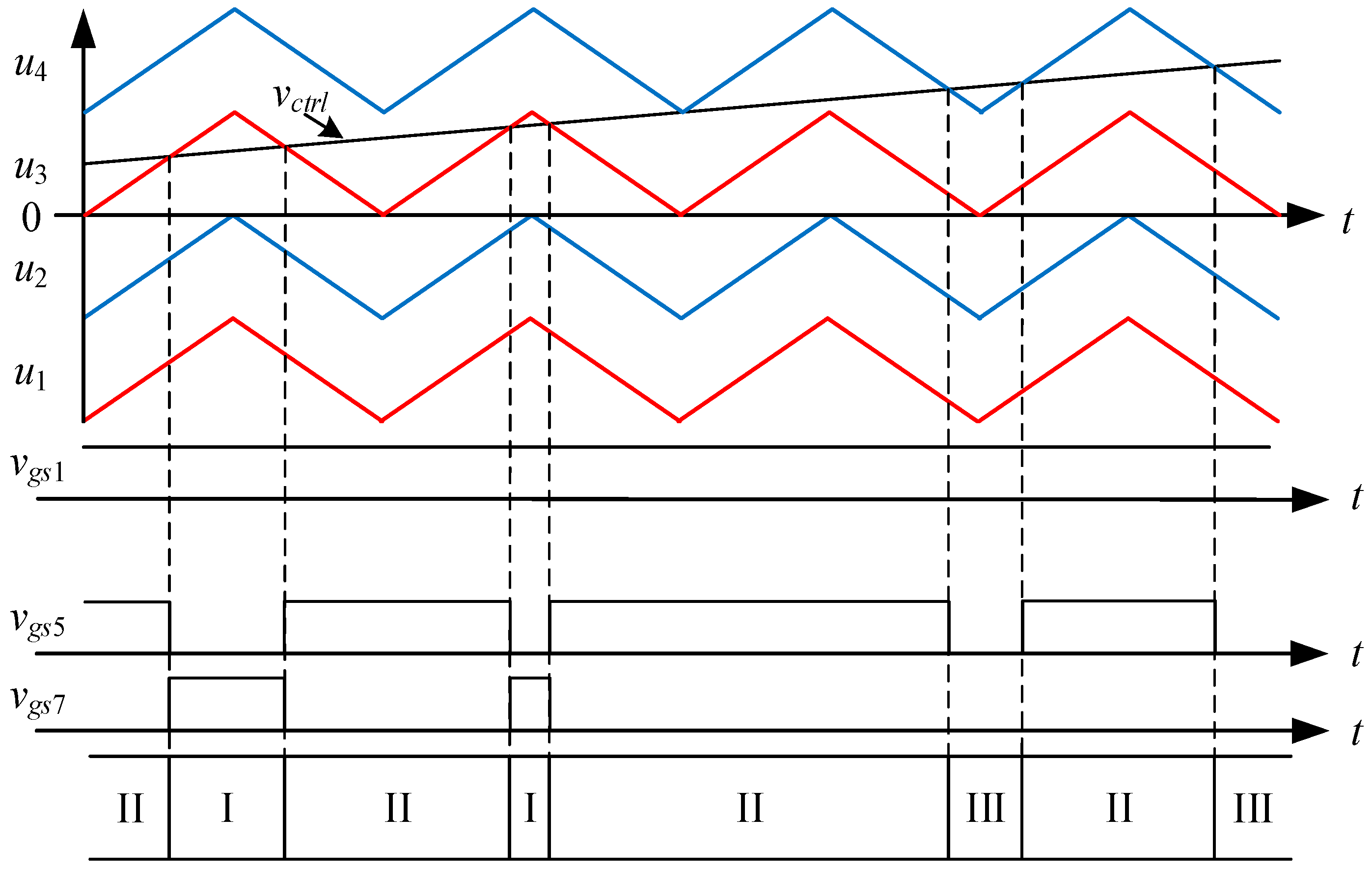
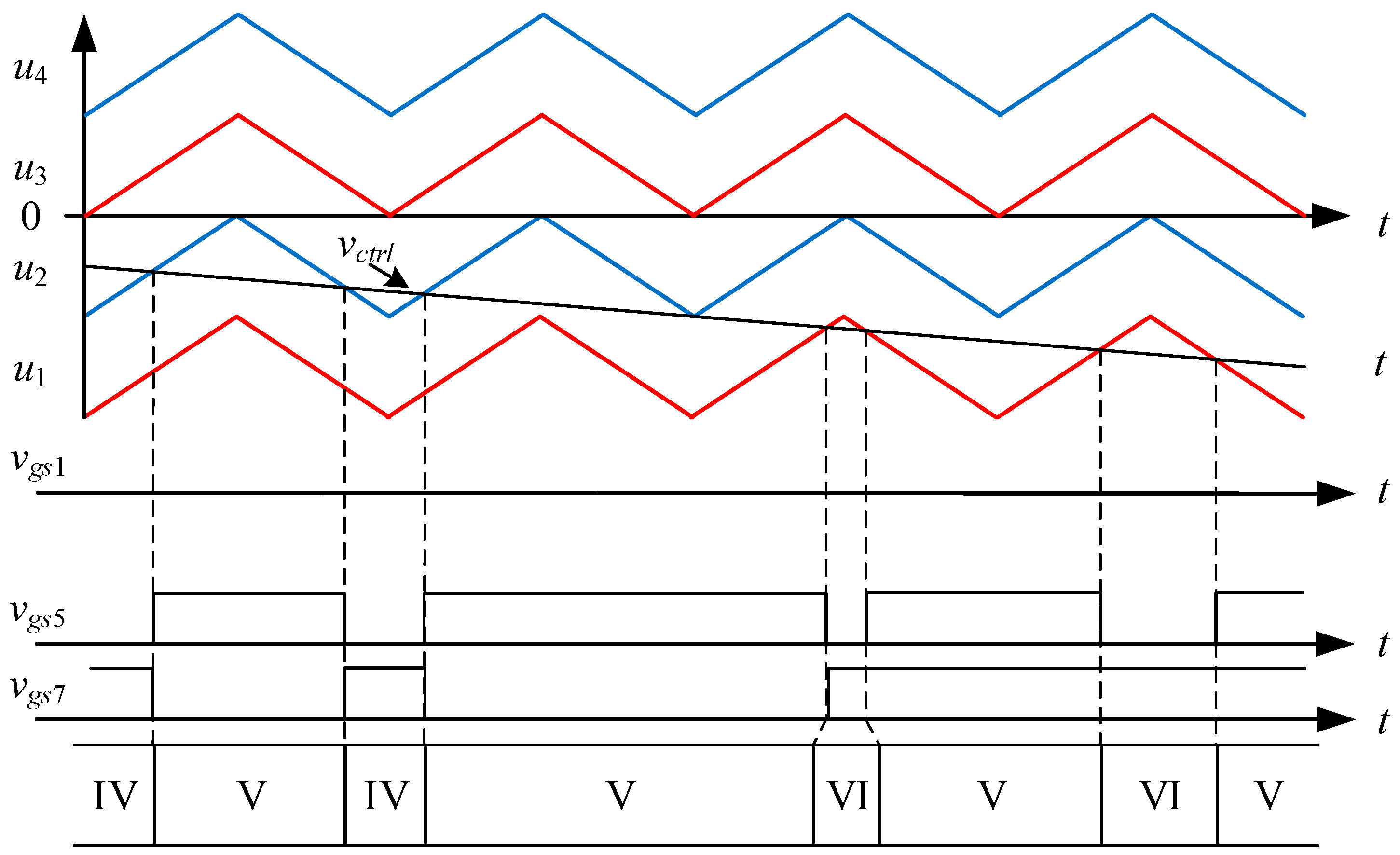
2.2. Operating Principles for Two Proposed Types of Circuits

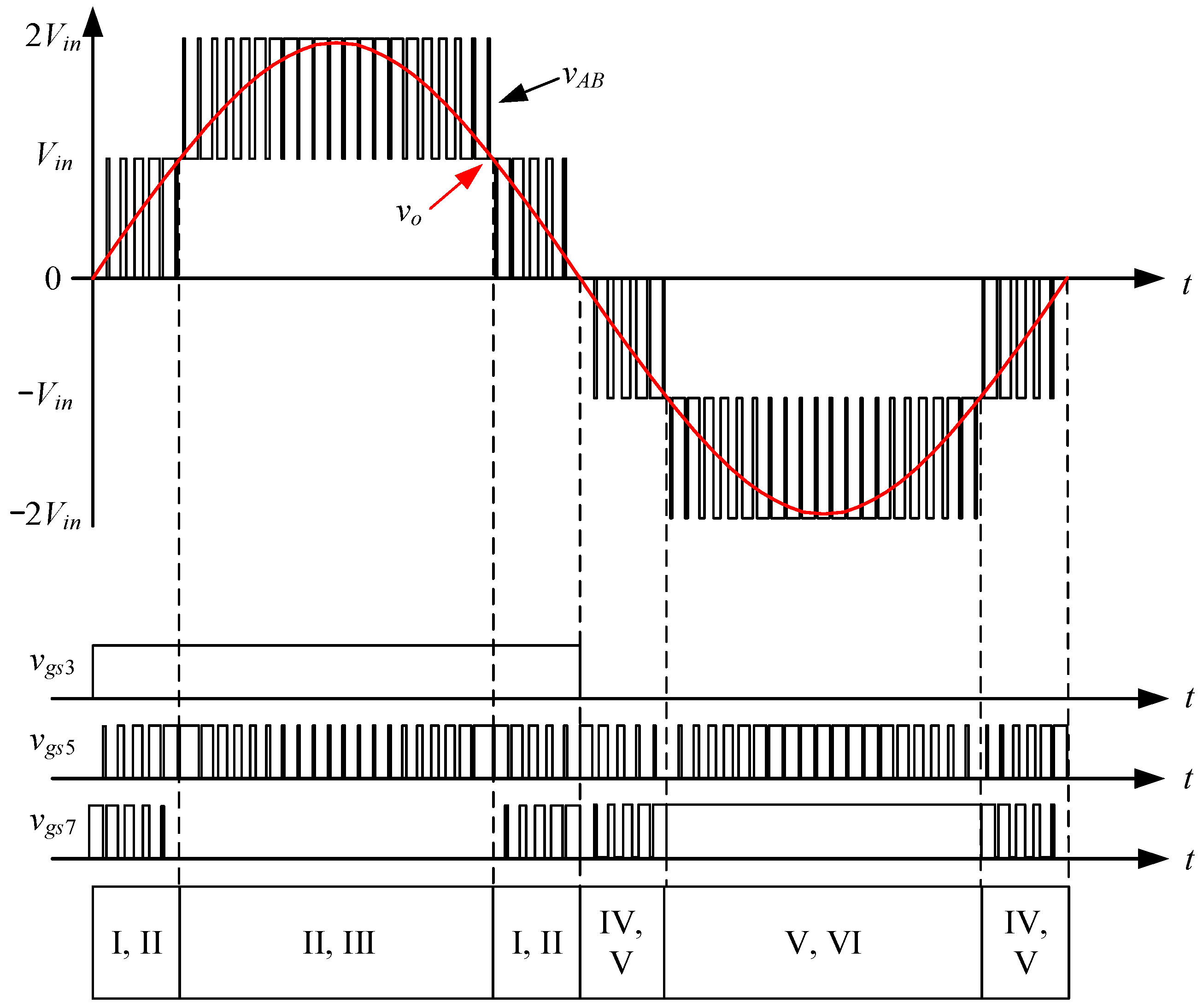
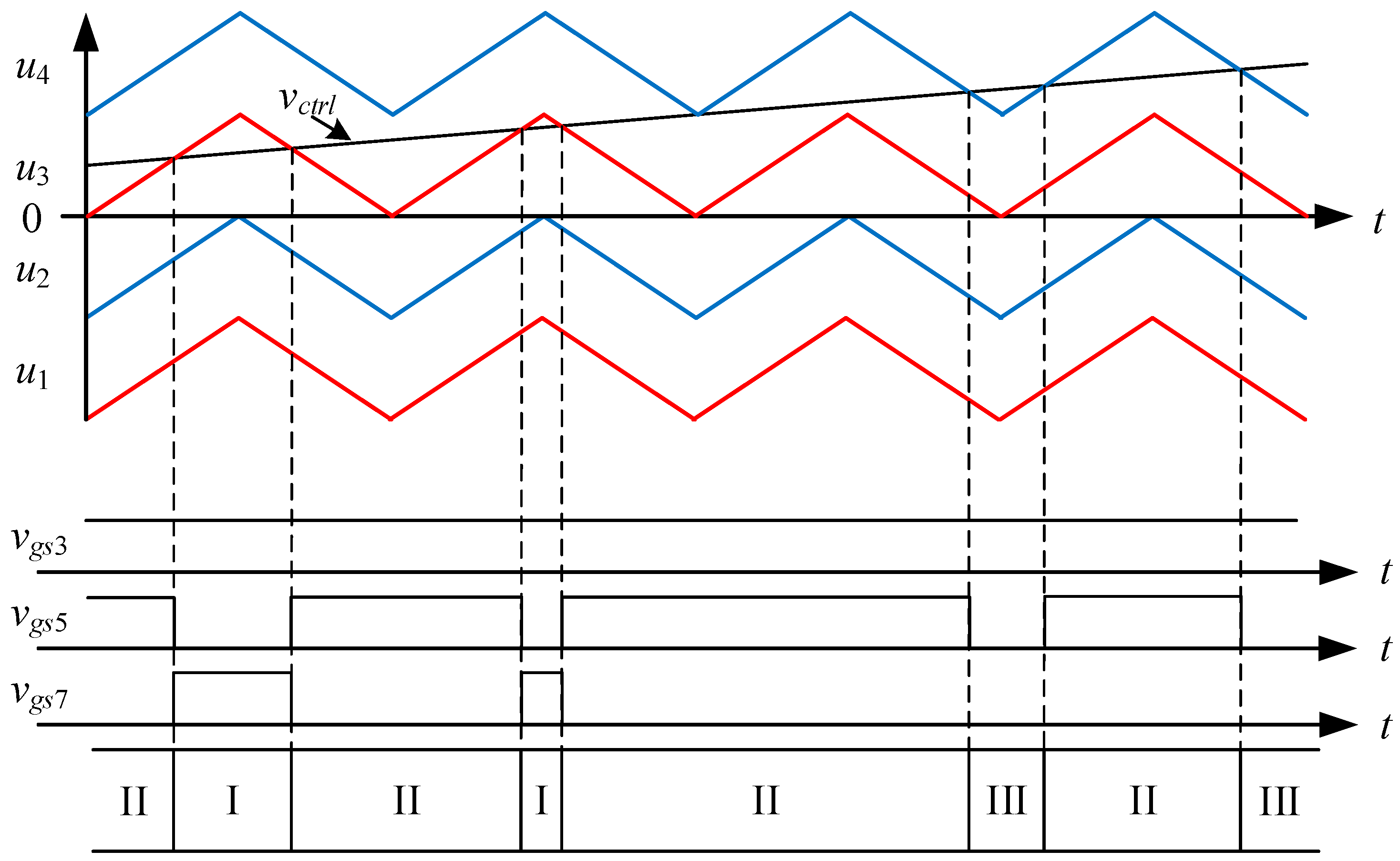
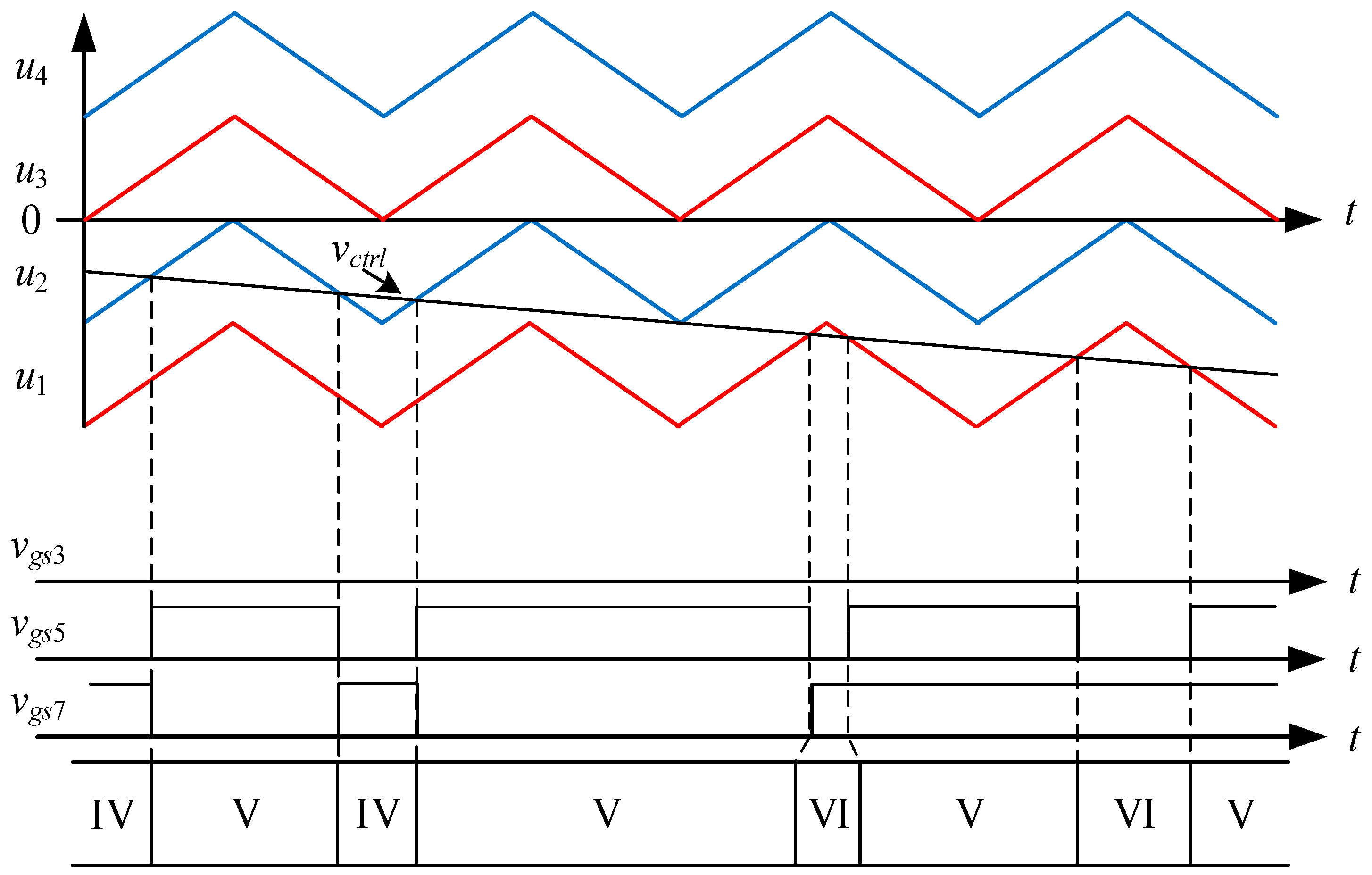
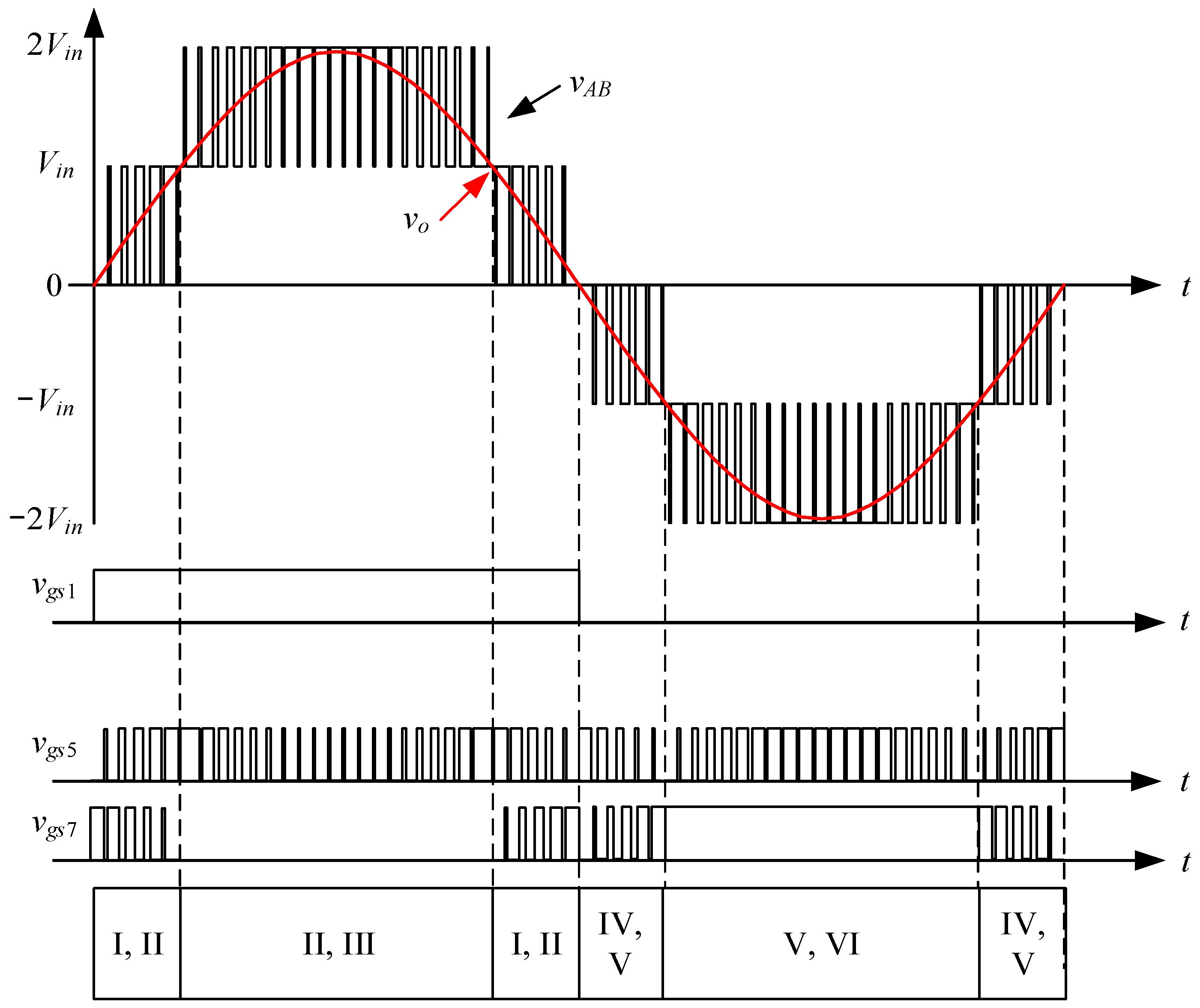
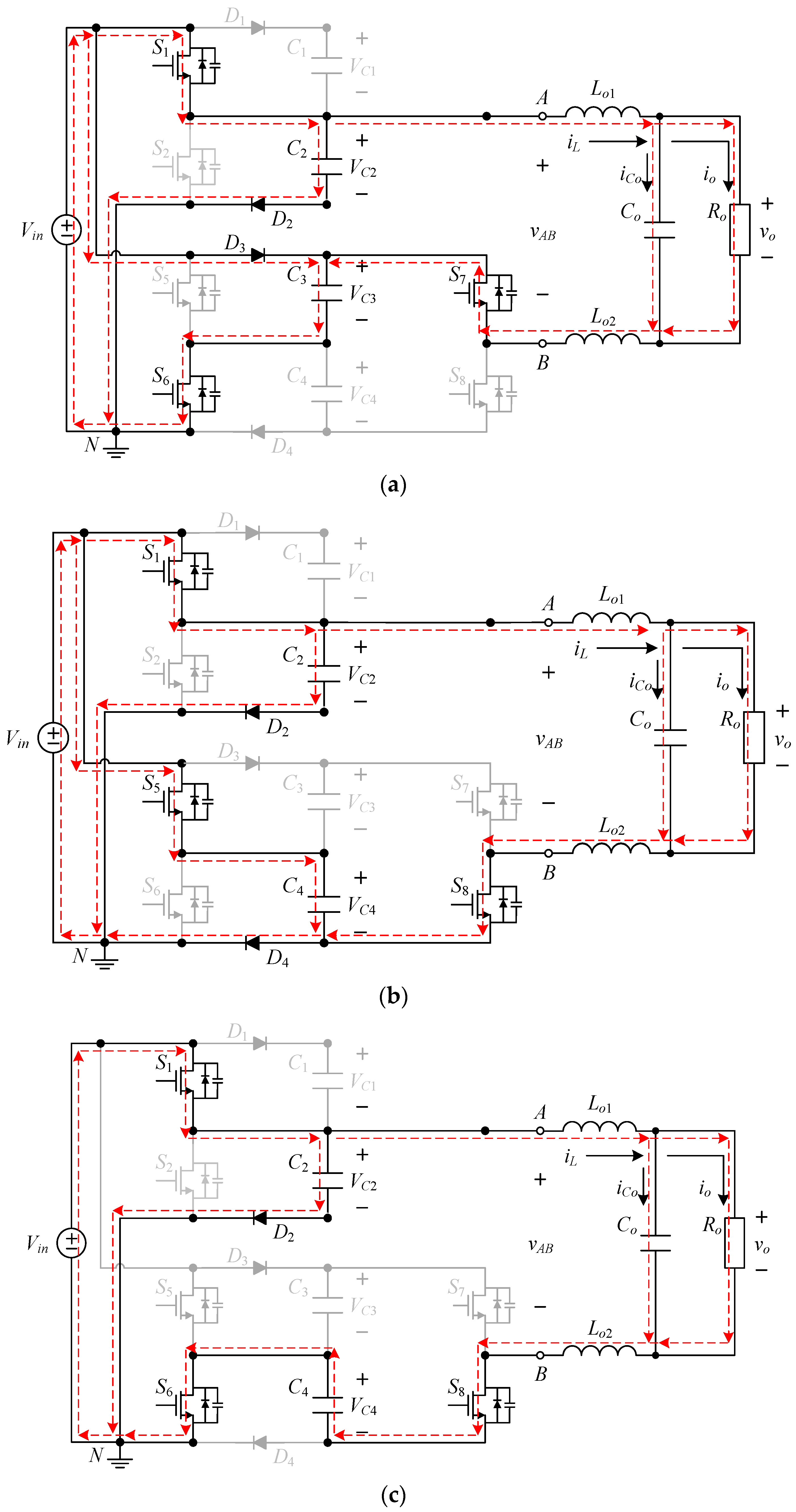
2.2.1. Type-1 Circuit

Figure 4 shows the waveforms of the switching signals for the proposed type-1 circuit, where the switches S1 and S2 are removed. There are six states of the circuit operation behavior, from state I to state VI.
When the output voltage operates in the positive half-cycle, the switch S3 always remains on. The inverter works between states I and II mainly by PWM-switching of S5 to establish the first voltage level, and the switch S7 is driven by the complementary signal of S5, whereas the inverter works between states II and III mainly by PWM-switching of S5 to establish the second voltage level, and at this time the switch S7 remains off.
When the output voltage operates in the negative half-cycle, the switch S3 always remains off. The inverter works between states IV and V mainly by PWM-switching of S7 to establish the first voltage level, and the switch S5 is driven by the complementary signal of S7, whereas the inverter works between states V and VI mainly by PWM-switching of S5 to establish the second voltage level, and at this time the switch S7 remains on.
In addition, the PWM gate driving signals of the switches S4, S6, and S8 are complementary to the gate driving signals of the switches S3, S5, and S7, respectively.
As shown in Figure 5, when the output voltage operates in the positive half-cycle, the control force vctrl performs LS-PWM with triangular waves u3 and u4. When the control force vctrl locates between zero and triangular wave u3, the inverter enters into state I. When the control force vctrl locates between triangular waves u3 and u4, the inverter enters into state II. When the control force vctrl is greater than triangular wave u4, the inverter enters into state III.
In addition, the gate driving signals of switches S4, S6, and S8 are complementary to the gate driving signals of switches S3, S5, and S7, respectively.
Furthermore, as shown in Figure 5, the output voltage of the type-1 circuit works in the positive half-cycle with two switching modes. By comparing the control force vctrl with the triangular wave u3, the inverter is switched between states I and II, and the duty cycle in state II is controlled as Da; by comparing the control force vctrl with the triangular wave u4, the inverter is switched between states II and III, and the duty cycle in state III is controlled as Db. The duty cycles Da and Db are shown in (1) and (2), respectively:
D a = v c t r l V m ,   0 < v c t r l < V m
D b = v c t r l V m 1 ,   V m < v c t r l < 2 V m
where Vm is the peak-to-peak value of the triangular waves u3 and u4.
State I [0 < vctrl < u3]: As shown in Figure 6a, the switches S3, S6, and S7 are on, and the switches S4, S5, and S8 are off. The inductor current iL will flow from the input voltage Vin through the switches S3, S6, and S7, and the diode D1 to form a loop. Therefore, the voltage between the terminals A and B is zero, namely, vAB = 0.
State II [u3 < vctrl < u4]: As shown in Figure 6b, the switches S3, S5, and S8 are on, and the switches S4, S6, and S7 are off. The inductor current iL will flow from the input voltage Vin through the switches S3 and S8 and the diodes D1 and D4 to form a loop. Therefore, the voltage between the terminals A and B is Vin, namely, vAB = Vin.
State III [u4 < vctrl]: As shown in Figure 6c, the switches S3, S6, and S8 are on, and the switches S4, S5, and S7 are off. The inductor current iL will flow from the input voltage Vin through the switches S3, S6, and S8 and the diode D1 to form a loop, and therefore, the voltage between the terminals A and B is 2 Vin, namely, vAB = 2 Vin.
As shown in Figure 7, when the output voltage operates in the negative half-cycle, the control force vctrl performs LS-PWM with triangular waves u1 and u2. When the control force vctrl locates between zero and triangular wave u1, the inverter enters into state IV. When the control force vctrl locates between triangular waves u1 and u2, the inverter enters into state V. When the control force vctrl is smaller than triangular wave u4, the inverter enters into state VI.
In addition, the gate driving signals of switches S3, S5, and S7 are complementary to the gate driving signals of switches S4, S6, and S8, respectively.
As shown in Figure 7, the output voltage of the type-1 circuit works in the negative half-cycle with two switching modes. By comparing the control force vctrl with the triangular wave u2, the inverter is switched between states IV and V, and the duty cycle in state V is controlled as Dc; by comparing the control force vctrl with the triangular wave u1, the inverter is switched between states V and VI, and the duty cycle in state VI is controlled as Dd. The duty cycles Dc and Db are shown in (3) and (4), respectively:
D c = v c t r l V m , V m < v c t r l < 0
D d = v c t r l V m 1 , 2 V m < v c t r l < V m
where Vm is the peak-to-peak value of the triangular waves u1 and u2.
State IV [u2 < vctrl < 0]: As shown in Figure 8a, the switches S4, S5, and S8 are on, and switches S3, S6, and S7 are off. The inductor current iL will flow from the input voltage Vin through the switches S4, S5, and S8 and the diode D2 to form a loop, and therefore, the voltage between the terminals A and B is zero, namely, vAB = 0.
State V [u1 < vctrl < u2]: As shown in Figure 8b, the switches S4, S6, and S7 are on, and the switches S3, S5, and S8 are off. The inductor current iL will flow from the input voltage Vin through the switches S4 and S7 and the diodes D2 and D3 to form a loop, and therefore, the voltage between the terminals A and B is −Vin, namely, vAB = −Vin.
State VI [vctrl < u1]: As shown in Figure 8c, the switches S4, S5, and S7 are on, and the switches S3, S6, and S8 are off. The inductor current iL will flow from the input voltage Vin through switches S4, S5, and S7 and the diode D2 to form a loop, and therefore, the voltage between the terminals A and B is −2 Vin, namely, vAB = −2 Vin.

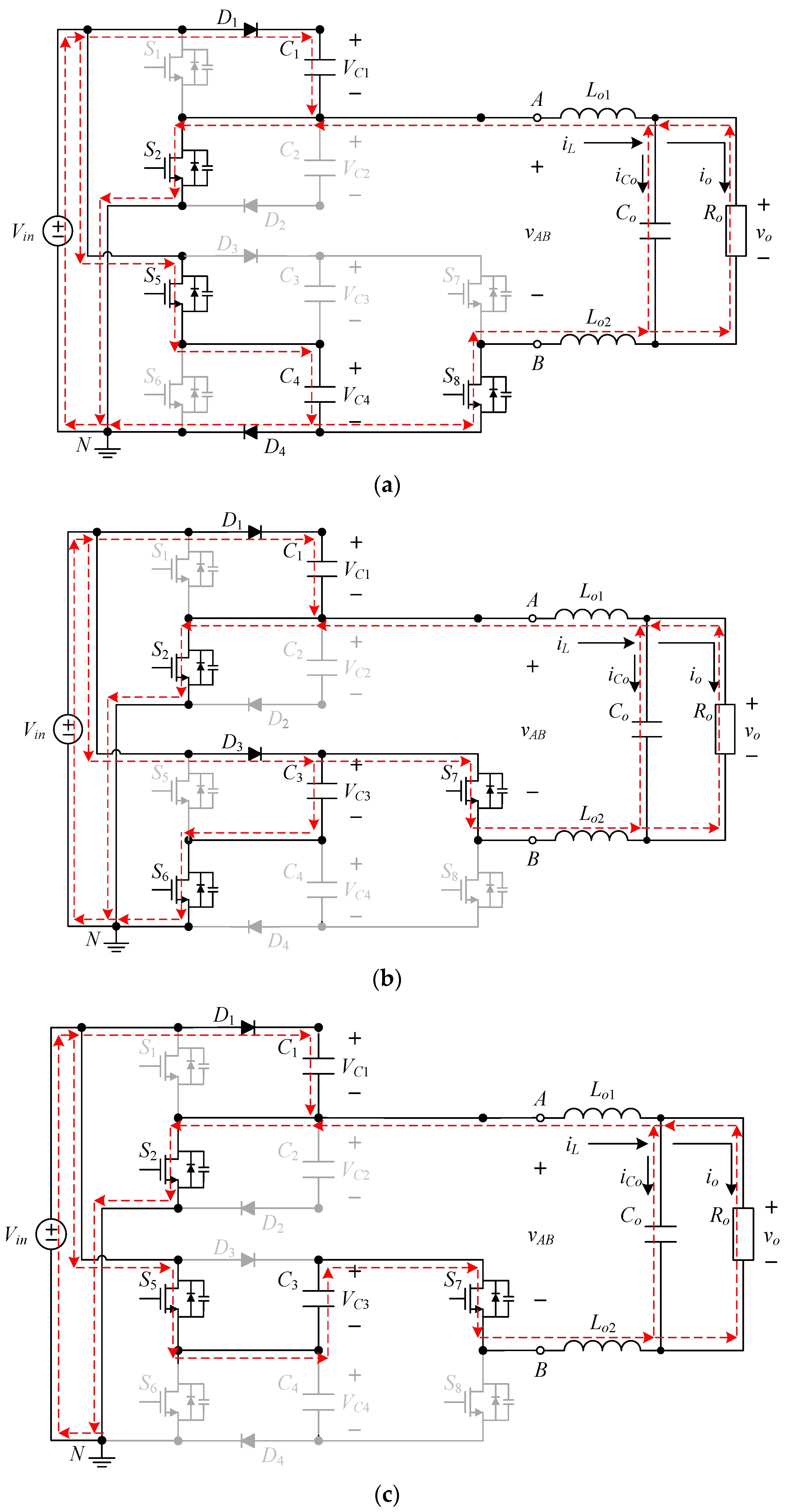
2.2.2. Type-2 Circuit

Figure 9 shows the waveforms of the switching signals of the proposed type-2 circuit, and there are six states of the circuit operation behavior. The signals vgs1 to vgs8 are the gate driving signals for switches S1 to S8.
When the output voltage operates in the positive half-cycle, the switch S1 always remains on, the inverter operates between states I and II mainly by PWM-switching of S5 to build up the first voltage level, and the switch S7 is driven by the complementary signal of S5, whereas the inverter operates between states II and III mainly by PWM-switching of S5 to build up the second voltage level, and at this time switch S7 remains on.
When the output voltage operates in the negative half-cycle, the switch S1 always remains off, the inverter operates between states IV and V mainly by PWM-switching of S7 to build up the first voltage level, and the switch S5 is driven by the complementary signal of S7, whereas the inverter operates between states V and VI mainly by PWM-switching of S5 to build up the second voltage level, and at this time the switch S7 remains on.
Moreover, the gate driving signals of switches S2, S6, and S8 are complementary to the gate driving signals of the switches S1, S5, and S7, respectively.
As shown in Figure 10, when the output voltage operates in the positive half-cycle, the control force vctrl does LS-PWM with triangular waves u3 and u4. When the control force vctrl locates between zero and triangular wave u3, the inverter enters into state I. When the control force vctrl locates between triangular waves u3 and u4, the inverter enters into state II. When the control force vctrl is larger than triangular wave u3, the inverter enters into state III.
Moreover, the gate driving signals of the switches S4, S6, and S8 are complementary to the gate driving signals of the switches S3, S5, and S7, respectively.
Furthermore, as shown in Figure 10, the output voltage of the type-2 circuit works in the positive half-cycle with two switching modes. By comparing the control force vctrl with the triangular wave u3, the inverter is switched between states I and II, and the duty cycle in state II is controlled as Da; by comparing the control force vctrl with the triangular wave u4, the inverter is switched between states II and III, and the duty cycle in state III is controlled as Db. In addition, the PWM-switching of the switches S5 to S8 in the type-2 circuit is the same as that in the type-1 circuit, so the duty cycles Da and Db in the type-2 circuit are the same as those in the type-1 circuit, as shown in (1) and (2).
State I [0 < vctrl < u3]: As shown in Figure 11a, the switches S1, S6, and S7 are on, and the switches S2, S5, and S8 are off. The inductor current iL will flow from the input voltage Vin through switches S1, S6, and S7 to form a loop, and therefore, the voltage between the terminals A and B is zero, namely, vAB = 0.
State 2 [u3 < vctrl < u4]: As shown in Figure 11b, the switches S1, S5, and S8 are on, and the switches S2, S6, and S7 are off. The inductor current iL will flow from the input voltage Vin through the switches S1, S8, and the diode D4 to form a loop, and therefore, the voltage between the terminals A and B is Vin, namely, vAB = Vin.
State 3 [u4 < vctrl]: As shown in Figure 11c, the switches S1, S6, and S8 are on, and the switches S2, S5, and S7 are off. The inductor current iL will flow from the input voltage Vin through the switches S1, S6, and S8 to form a loop, and therefore, the voltage between the terminals A and B is 2 Vin, namely, vAB = 2 Vin.
As shown in Figure 12, when the output voltage operates in the negative half-cycle, the control force vctrl performs LS-PWM with triangular waves u1 and u2. When the control force vctrl locates between zero and triangular wave u1, the inverter enters into state IV. When the control force vctrl locates between triangular waves u1 and u2, the inverter enters into state V. When the control force vctrl is smaller than triangular wave u4, the inverter enters into state VI.
Moreover, the gate driving signals of switches S3, S5, and S7 are complementary to the gate driving signals of switches S4, S6, and S8, respectively.
Furthermore, as shown in Figure 12, the output voltage of the type-2 circuit works in the negative half-cycle with two switching modes. By comparing the control force vctrl with the triangular wave u2, the inverter is switched between states IV and V, and the duty cycle in state V is controlled as Dc; by comparing the control force vctrl with the triangular wave u1, the inverter is switched between states V and VI the duty cycle in state VI is controlled as Dd.
Moreover, since the PWM-switching of the switches S5 to S8 in the type-2 circuit are the same as that in the type-1 circuit, the duty cycles Dc and Dd in the type-2 circuit are identical to those in the type-1 circuit, as shown in (3) and (4).
State 4 [u2 < vctrl < 0]: As shown in Figure 13a, the switches S2, S5, and S8 are on and the switches S1, S6, and S7 are off. The inductor current iL will flow from the input Vin voltage through the switches S2, S5, and S8 to form a loop, and therefore, the voltage between the terminals A and B is zero, namely, vAB = 0.
State 5 [u1 < vctrl < u2]: As shown in Figure 13b, the switches S2, S6, and S7 are on and the switches S1, S5, and S8 are off. The inductor current iL will flow from the input voltage Vin through the switches S2, S6, and S7 and the diode D3 to form a loop, and therefore, the voltage between terminals A and B is −Vin, namely, vAB = −Vin.
State 6 [vctrl < u1]: As shown in Figure 13c, the switches S2, S5, and S7 are on and the switches S1, S6, and S8 are off. The inductor current iL will flow from the input voltage Vin through the switches S2, S5, and S7 to form a loop, and therefore the voltage between the terminals A and B is −2 Vin, namely, vAB = −2 Vin.

2.3. Converter Component Operating Behavior

For clarity and completeness, Table 2 shows the switch behavior and clamping capacitor charging/discharging behavior of type-1 and type-2 circuits.
In addition, based on the above analysis, Table 3 shows the switching status of the proposed five-level MLIs and their corresponding output voltages, together with the existing three circuits shown in Figure 1, are employed as comparisons. From this table, it can be seen that the voltage gains of the proposed inverters have two times those of the existing topologies.

3. System Design

3.1. System Configuration

Figure 14 shows the system block diagram of the switched-capacitor five-level DC-AC inverter. The system configuration includes the main power stage containing a type-1 circuit or type-2 circuit, the gate drivers, and the output voltage feedback circuit containing the voltage divider, FPGA, DAC, and voltage sampling circuit without ADC. The operating principle of the main stage has already been discussed in the previous section, and the UCC21540 isolated driver is used as the gate driving circuit. In terms of the voltage feedback circuit, the output voltage vo is divided into a small voltage signal vod, and the reference voltage vref is subtracted from vod to obtain an error signal which will be modulated into a pulse signal vpulse via no ADC sampling technique [50]. After this, this signal vpulse is sent to the FPGA with the PI controller embedded and converted to a signal vFB, which will be then compensated to obtain the corresponding gate driving signals. Table 4 shows the specifications of the proposed switched-capacitor five-level DC-AC inverter.

3.2. Design of Clamping Capacitor

In this paper, the AC output voltage frequency fline is set at 60 Hz, which can be converted to an angular frequency of 377 (rad/s), and the time instants of clamping capacitor discharge in the positive half-cycle are calculated based on (5) to (8), which are shown as follows:
t 1 = sin 1 ( 2 3 ) ω = 1.936 ms
t 2 = π 2 ω 0.5 f s = 4.1581 ms
t 3 = π 2 ω + 0.5 f s = 4.1752 ms
t 4 = π ω t 1 = 6.398 ms
The clamping capacitors used in the inverter can be divided into two classes according to the charging and discharging time. States III and IV are taken as examples. Figure 15 displays that the clamping capacitor C1 in the first class is used as a DC power source for discharging when entering state III and providing state IV operation, whereas the clamping capacitor C4 in the second class is used for fast charging and discharging behavior in accordance with the transition between these two states.
The maximum discharging charge of clamping capacitors C1 and C4 in the positive half-cycle can be calculated from (9) and (10) as follows:
Δ Q 1 = t 1 t 4 2 I o , r a t e d sin ω t d t = 25.43 mC
Δ Q 4 = t 2 t 3 2 I o , r a t e d sin ω t d t = 109.7 μ C
In general, the ripple voltage on the capacitor is 1% of the DC voltage across it, so the corresponding ripple voltage is shown below:
Δ V = 58 × 0.01 = 0.58 V
Generally acknowledged, the amount of voltage change is proportional to the amount of charge change. As far as the symmetrical circuit structure is concerned, the clamping capacitance of C3 is equal to the capacitance of C1, and in the same way, the clamping capacitance of C2 is equal to the capacitance C4. Substituting (9)–(11) into (12) and (13) yields the clamping capacitances of C1 to C4 as follows:
C 1 = C 3 = Δ Q 1 Δ V = 25.43 mC 0.58 V = 43 . 837 mF
C 4 = C 2 = Δ Q 4 Δ V = 109.7 μ C 0.58 V = 189 μ F
In (12), the value of C1 and C3 is calculated to be 43 . 837 mF , which is too large for the 250 W DC-AC inverter. Therefore, the output voltage must not be affected by appropriate reduction of this capacitance, so the actual test of the capacitor ripple voltage is fixed at 4 V to get a better result, and re-substitution of this value into (12) can obtain (14) as follows:
C 1 = C 3 = C = Δ Q 1 Δ V = 25.43 mC 4 V = 6 . 356 mF
The capacitors C1 to C4, which are analyzed in the previous section for the type-1 and type-2 circuits, will be charging and discharging in accordance with the switching frequency, so it is sufficient to use the same capacitance of 6 . 356 mF for these capacitors. In addition, according to the analysis of the circuit operation principle, it can be seen that the voltages across such clamping capacitors are approximately equal to the input voltage. Since the electrolytic capacitors used should be derated, the rated voltage of the selected capacitors should be more than 1.5 times of the input voltage, that is,
V C , r a t e d 1.5 × 58 = 87 V
Eventually, two 3.3 mF electrolytic capacitors paralleled can be used for these four capacitors.

3.3. Design of High Frequency Low-Pass Filter

When the inverters operate, the THD of the utility voltage supplied by the power company should be taken into account. According to the IEEE 519 standard [3], the total harmonic voltage distortion limit is 8% or less below 1 kV, implying that each harmonic voltage distortion should be 5% or less.
The harmonic components of the output voltage from a high-frequency switching inverter can be categorized into two cases. One is low-frequency harmonics generated by the fundamental waveform of the output voltage, locating between several to several tens of times of the line frequency, and the other is high-frequency harmonics generated by the switching of the switch. In the former case, the controller can be used for the closed-loop control to reduce the low-frequency harmonics by increasing the loop gain. In the latter case, the low-pass filter can be used to reduce the high-frequency harmonics.
As shown in Figure 16, the inductors Lo1 and Lo2 and the capacitor Co are used to construct this second-order low-pass filter.
Due to the characteristics of the multi-level output voltage, it is possible to add a second-order low-pass filter with a higher cutoff radian frequency and the corresponding transfer function is as follows:
H s = v o ( t ) v A B ( t ) = V o ( s ) V A B ( s ) = 1 s 2 ω c 2 + s Q ω c + 1 = 1 s 2 L C o + s L R o + 1
where L = L o 1 + L o 2 ; and the cutoff radian frequency is ω c = 1 L C o , and the quality factor Q = R o C o L .
As shown in (17), the peak-to-peak ripple voltage vrpp of the inverter is limited to 0.01 times of the maximum output voltage to reduce the high-frequency harmonic components of the output voltage. Equation (18) is used to calculate the value of vrpp generated during the switching period. Since the operating principle of the inverter is similar to that of a buck inverter, the calculation method shown in [51] is adopted. Also, the peak-to-peak value of the inductor current generated during the switching period is shown in (19):
v r p p = 0.01 Gain V i n = 0.01 × 3 × 58 = 1 . 74 V
v r p p = 1 2 Δ i L 2 1 2 f s 1 C o
Δ i L = V i n . D . ( 1 D ) L . f s
Substituting (19) into (18) yields the effect of the filter inductor L and filter capacitor Co on vrpp, as shown in (20). In (20), it is also known that the maximum value of vrpp will happen when the duty cycle D is 0.5. Therefore, substituting (20) into (21) yields and the cutoff frequency is fc, as shown in (22):
v r p p = V i n D ( 1 D ) 8 L C o f s 2 = V i n D ( 1 D ) 8 ω c 2 f s 2
ω c = 8 v r p p V i n D ( 1 D ) f s = 8 1.74 58 0.5 ( 1 0.5 ) 58.6 kHz = 57416.04   ( rad / s )
f c = ω c 2 π = 9.138   kHz
In (16), the relationship between the filter inductance L, the filter capacitance Co, the load resistance Ro, and the cut-off radian frequency on the quality factor Q can also be obtained. Therefore, the value of Q at rated load is set at the inverse value of 0.707, and then the values of L and Co can be obtained as shown in (23) and (24), respectively:
L = R o Q ω c = 24.2 1.414 57416.04 = 298 μ H
C o = Q R ω c = 1.414 24.2 57416.04 = 1.02 μ F
Eventually, a 1 μF metal film capacitor, manufactured by HJC Co., Seoul, Republic of Korea [52], is chosen.

4. Verification Based on Simulation and Experiment

In this section, the results of the proposed switched-capacitor five-level single-phase DC-AC inverters are simulated and experimented. First, the design parameters obtained in the previous section are put into the circuits to construct the PSIM simulation environment to simulate the closed-loop control of the proposed inverters so that the feasibility of the proposed two circuits can be demonstrated. After this, the FPGA is used as the digital control kernel to obtain experimental results so as to verify their effectiveness.

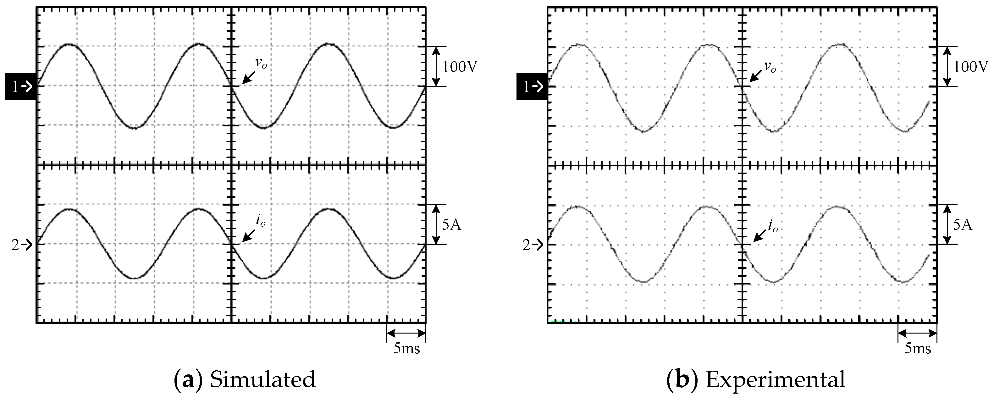
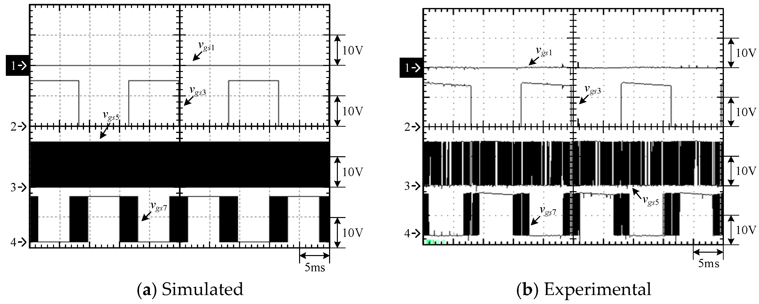
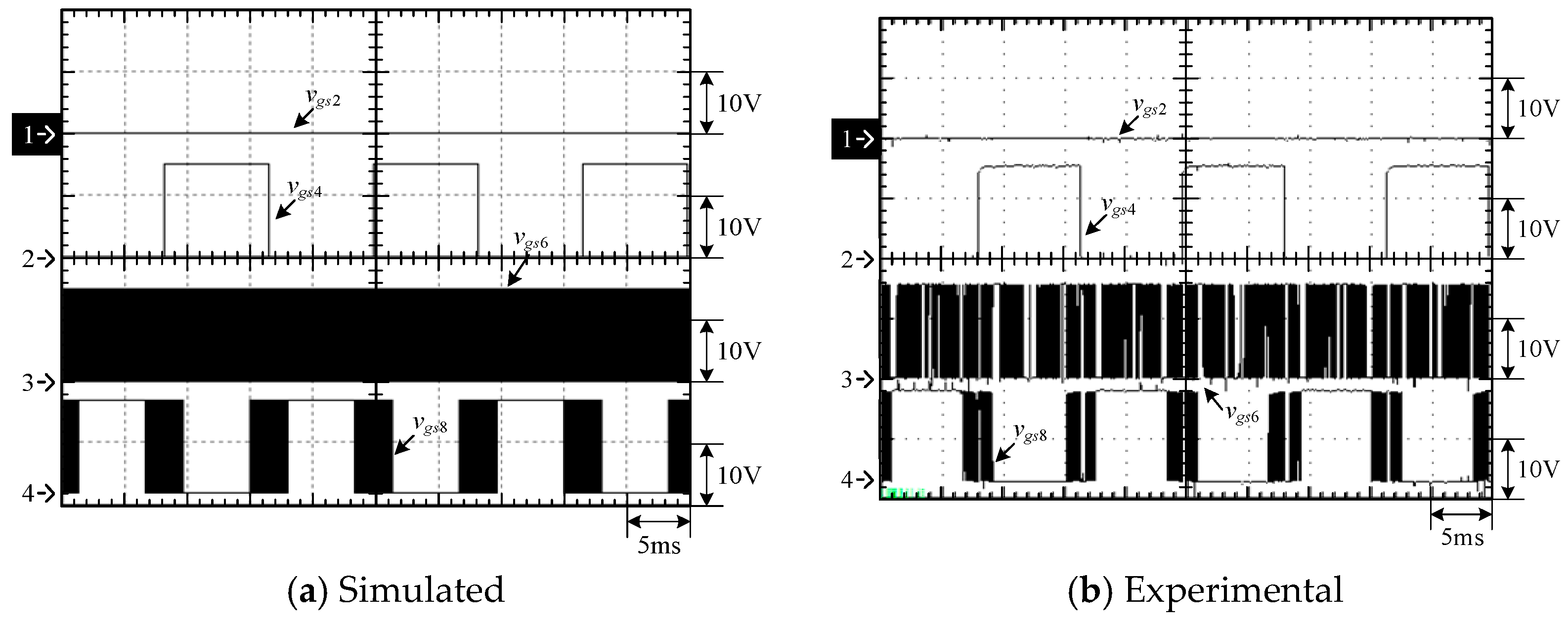
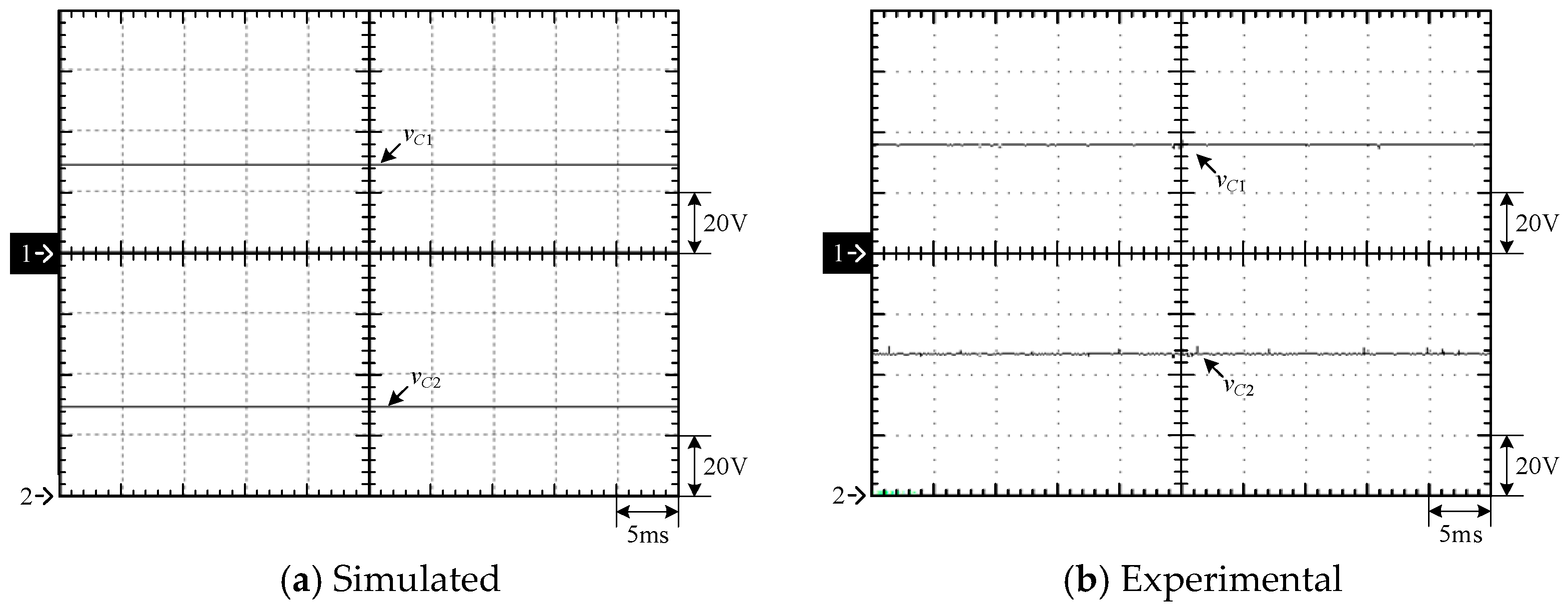
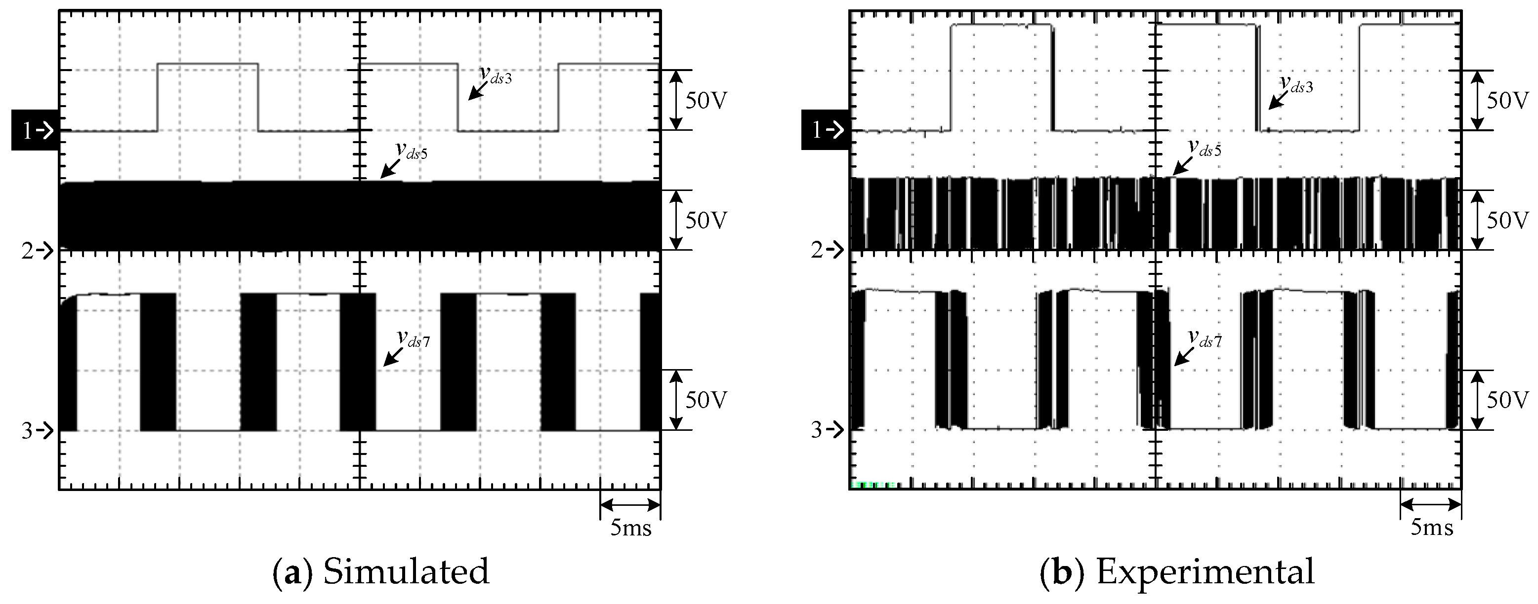
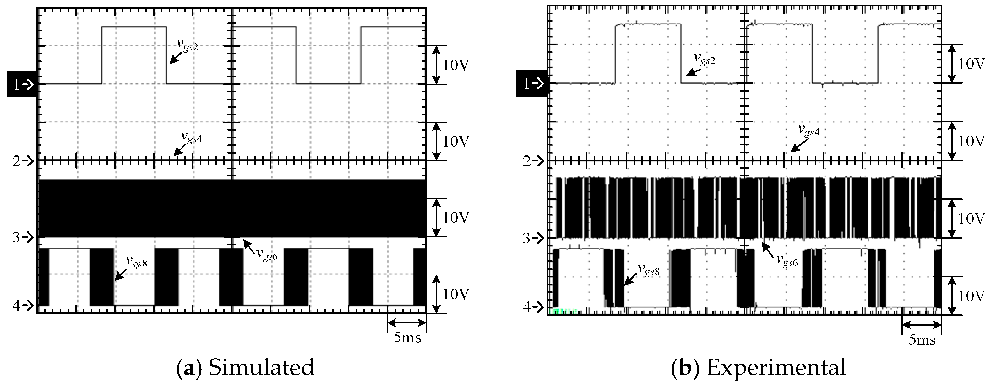
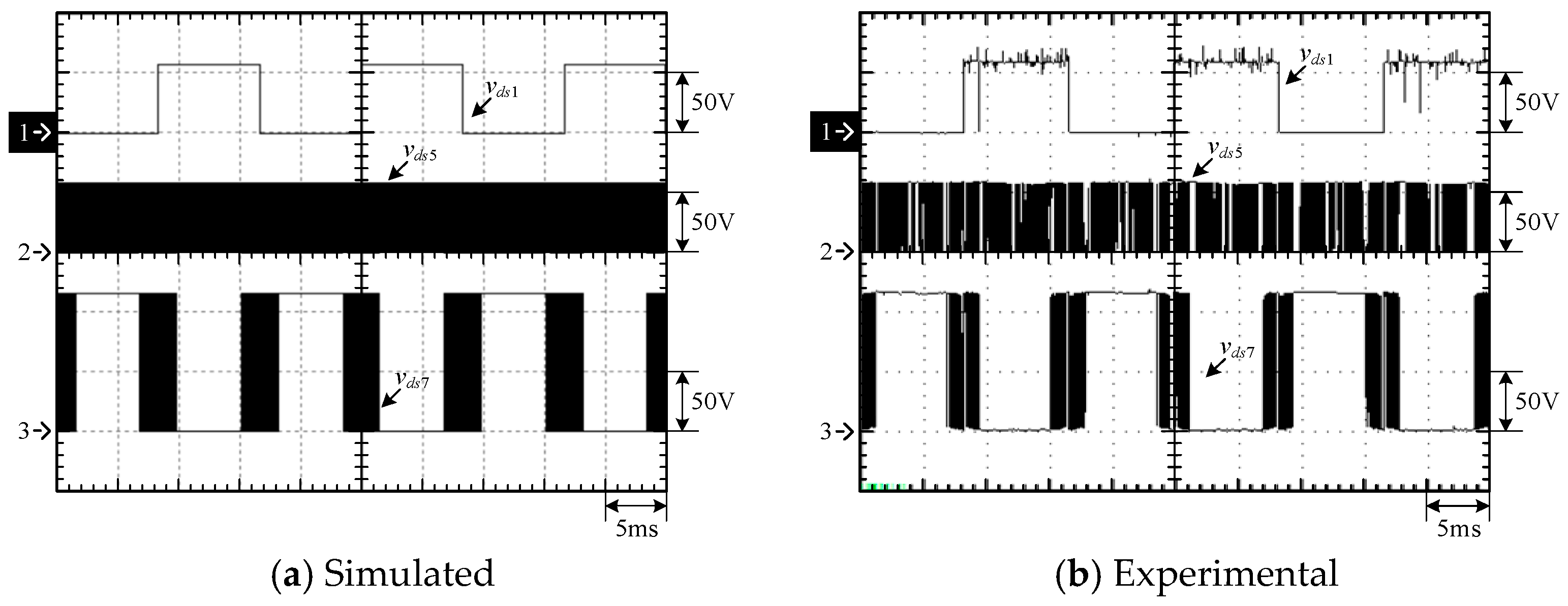
4.1. Simulated and Experimental Waveforms of Type-1 Circuit

Under the type-1 circuit at rated load, Figure 17 shows the output voltage vo and output current io. Figure 18 shows the output voltage vo and the unfiltered output voltage vAB. Figure 19 shows the gate driving signals vgs3, vgs5, and vgs7 for the switches S3, S5, and S7, respectively. Figure 20 shows the gate driving signals vgs4, vgs6, and vgs8 for the switches S4, S6, and S8, respectively. Figure 21 shows the voltages across the clamping capacitors C1 and C2, called vC1 and vC2, respectively. Figure 22 shows the voltages across the clamping capacitors C3 and C4, called vC3 and vC4, respectively. Figure 23 shows the voltages across the switches S3, S5, and S7, called vds3, vds5, and vds7, respectively. Figure 24 shows the voltages across the switches S4, S6, and S8, called vds4, vds6, and vds8, respectively.

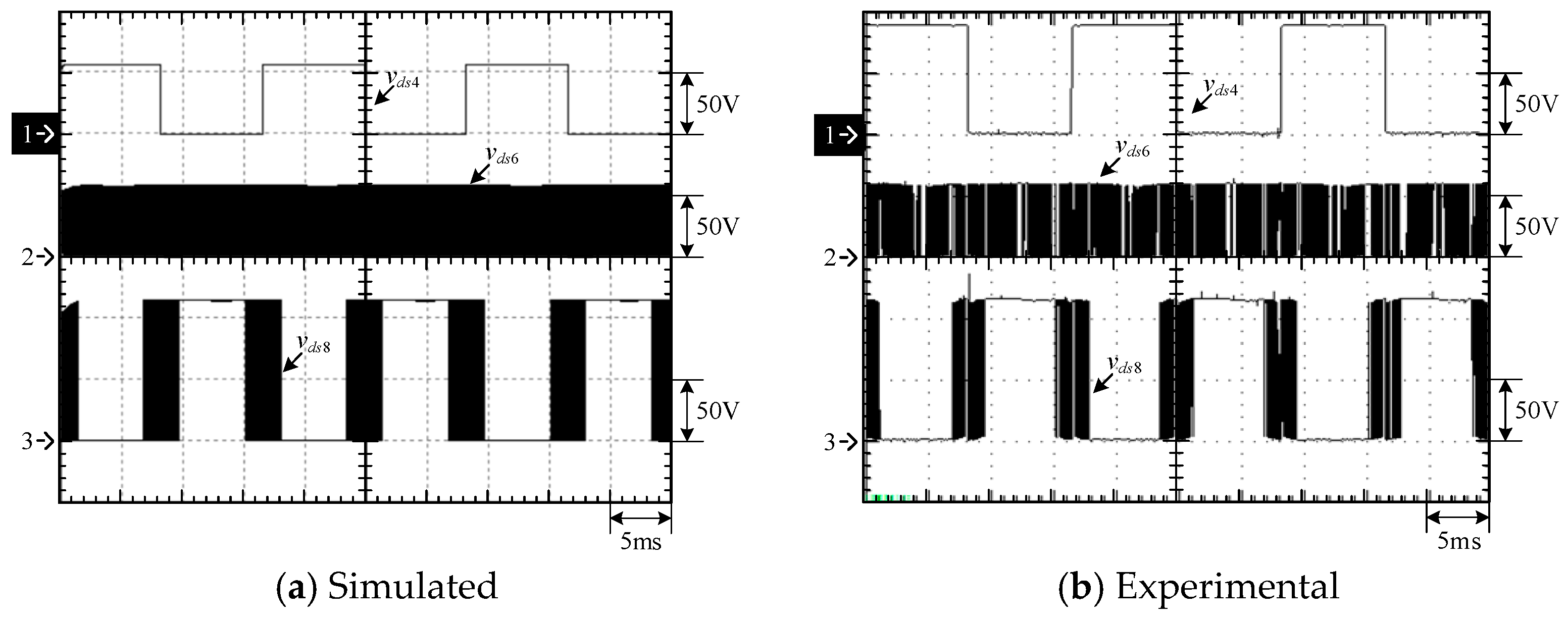
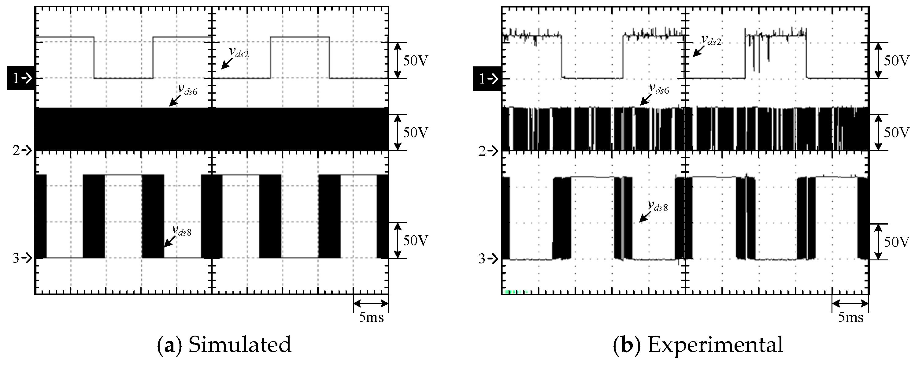
4.2. Simulated and Experimental Waveforms s of Type-2 Circuit

Under the type-2 circuit at rated load, Figure 25 shows the output voltage vo and output current io. Figure 26 shows the output voltage vo and the unfiltered output voltage vAB. Figure 27 shows the gate driving signals vgs3, vgs5, and vgs7 for the switches S3, S5, and S7, respectively. Figure 28 shows the gate driving signals vgs4, vgs6, and vgs8 for the switches S4, S6, and S8, respectively. Figure 29 shows the voltages across the clamping capacitors C1 and C2, called vC1 and vC2, respectively. Figure 30 shows the voltages across the clamping capacitors C3 and C4, called vC3 and vC4, respectively. Figure 31 shows the voltages across the switches S3, S5, and S7, called vds3, vds5, and vds7, respectively. Figure 32 shows the voltages across the switches S4, S6, and S8, called vds4, vds6, and vds8, respectively.

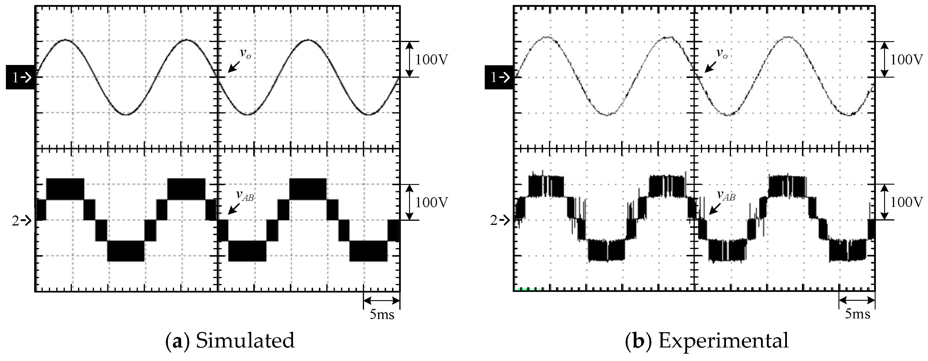
4.3. Waveform Comparison of the Two Types

From the waveforms in Figure 19, Figure 20, Figure 21, Figure 22, Figure 23 and Figure 24, it can be seen that the type-1 circuit adopts the PWM-switching of mixing high and low speeds to generate the gate driving signals to drive the switches. The switches S3 and S4 switch with the output frequency, and the switches S5 to S8 switch with the high frequency to get the unfiltered output voltage vAB, and then the output voltage vo and output current io with low harmonic components are obtained through the filter. Moreover, the switching behavior of the switch is ignored by the blanking time, and this is because the switching period under this control state is too small, so the corresponding waveforms are not controlled. Accordingly, the gate driving signal of the switch can be seen as part of the switching cycle with the constant cutoff period. Figure 22 shows the clamping capacitors C3 and C4, which are clamped at the input voltages by switching the diodes D3 and D4, and the switches S5 and S6, with the result that the voltages across the clamping capacitor C3 and C4, called vC3 and vC4, are clamped at the input voltage. As shown in Figure 23 and Figure 24, the switches S3 and S4 are connected across the two ends of two series capacitors C1 and C2; the maximum voltages across the switches S3 and S4 are the sum of the voltages across the clamping capacitors C1 and C2, called vC1 and vC2. Similarly, the switches S7 and S8 are connected across the two ends of two series capacitors C3 and C4, and it is known that the capacitors C3 and C4 are clamped at the input voltages, so the maximum voltages across the switches S7 and S8 are two times the input voltage. Therefore, the switches S7 and S8 have to withstand twice the input voltage, while the switches S5 and S6 are connected to the input voltage, i.e., they only have to withstand the input voltage. In addition, due to the switch-opened detection being embedded in the experiment, the corresponding voltages across the switches have part of the blanking time, thereby making the experimental waveforms different from the simulated waveforms.
From the waveforms in Figure 25, Figure 26, Figure 27, Figure 28, Figure 29, Figure 30, Figure 31 and Figure 32, it can be seen that the type-2 circuit adopts the PWM-switching of mixing high and low speeds to generate the driving signals to drive the switches. The switches S1 and S2 switch with the output frequency, and the switches S5 to S8 switch with the high frequency to get the unfiltered output voltage vAB, and then the output voltage vo and output current io with low harmonic components are obtained through the filter. In addition, the switching behavior of the switch is ignored by the blanking time, and this is because the switching period under this control state is too small, so the corresponding waveforms are not controlled. Accordingly, the gate driving signal of the switch can be seen as part of the switching cycle with the constant cutoff period. Figure 30 shows the voltages across the clamping capacitors C3 and C4, called vC3 and vC4, are switched by the switches S5 and S6 to clamp the clamping capacitors C3 and C4 to the input voltage. As can be seen from Figure 31 and Figure 32, the switches S7 and S8 are connected across the two ends of the two series capacitors C3 and C4, and since the two clamping capacitors C3 and C4 are clamped at the input voltage, so the maximum voltages across the switches S7 and S8 are two times the input voltage, whereas the switches S1, S2, S5, and S6 are connected across the input voltage so the maximum voltages across them are the input voltage. Moreover, due to the switch-opened detection being embedded in the experiment, the corresponding voltages across the switches also have part of the blanking time, thus causing the experimental waveforms to be different from the simulated waveforms.

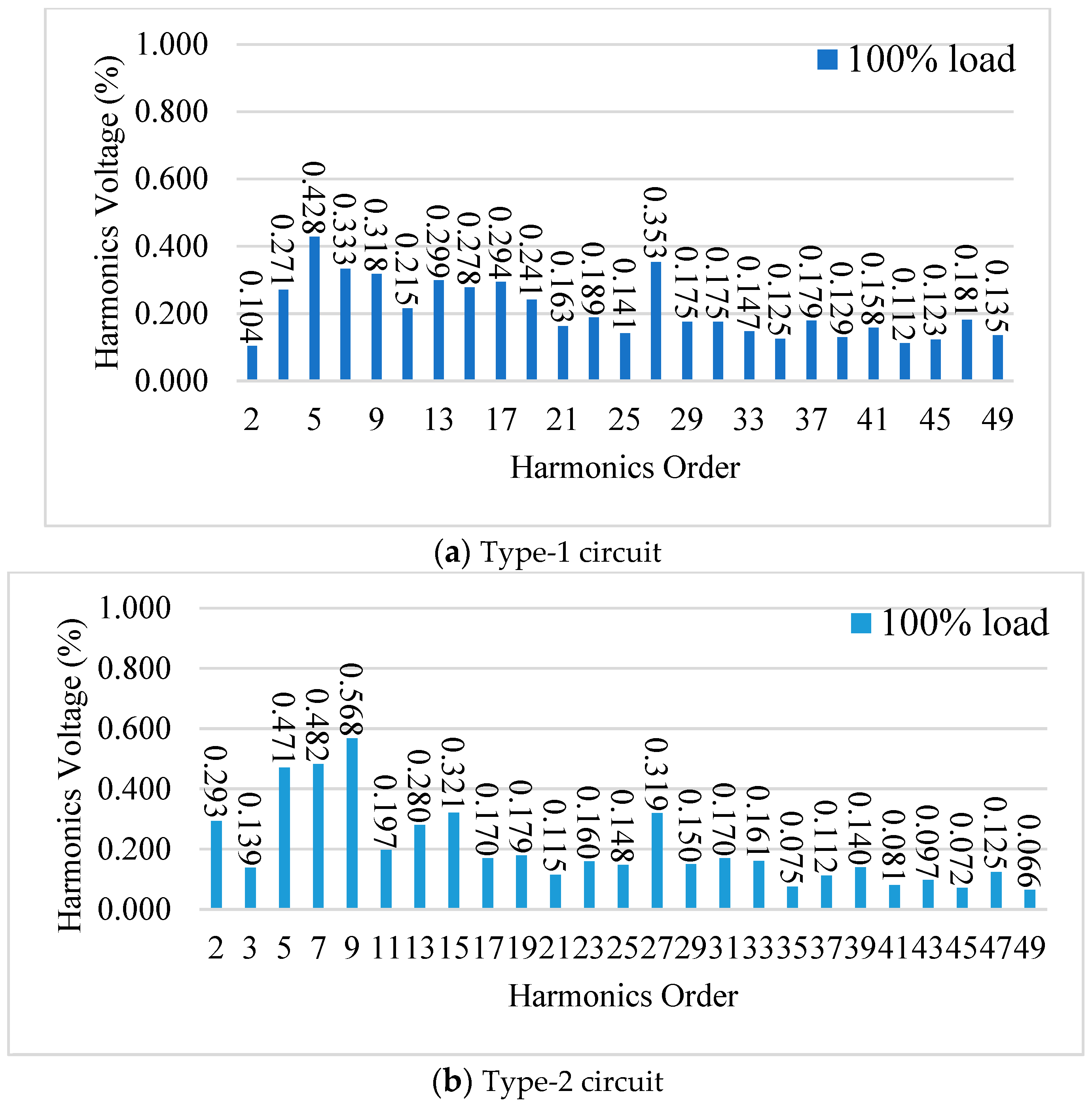
4.4. Harmonic Distribution and Efficiency of Two Types

Figure 33a,b show the harmonic distribution of the output voltage at rated load for the type-1 and type-2 circuits, respectively. From these figures, the values of THD, measured by the power analyzer (PM1000+), are 0.71% and 0.78% for the type-1 and type-2 circuits, respectively. All these values of THD comply with IEEE 519-2014, which states that the THD of harmonics voltage should be less than 8%.
Figure 34a,b show the curves of efficiency versus output power for the type-1 and type-2 circuits, respectively. From Figure 34a, it can be seen that for the type-1 circuit, the maximum efficiency is 97.43% and the minimum efficiency is 95.81%, whereas for the type-2 circuit, the maximum efficiency is 96.87% and the minimum efficiency is 95.80%, respectively. This is because these two circuits are designed to reduce the number of power-switching times by using a mixed high and low speed control strategy. However, the load current will flow through the diode, and the accompanying conduction loss caused will affect the overall efficiency, i.e., the higher the load is, the lower the efficiency.

4.5. Comparison between the Recent Related MLIs

Under the condition of the same number of DC power sources, a comparison of the recent papers presented for the five-level single-phase DC-AC inverters [2,31,43,44,45,46,47,48,49] with various criteria and feature emphases is tabulated in Table 5. Additionally, in this table, the full names for all the abbreviations of control strategies are shown in Table 6. From Table 5, it can be seen that the THD of the proposed inverters is least among those of the recent related inverters.

5. Conclusions

In this paper, two types of asymmetric switched-capacitor five-level single-phase DC-AC inverters are presented based on the clamping half-bridge circuit and the output half-bridge circuit. Furthermore, the half-bridge gate drivers can be used to drive the switches. From the measured results, the type-1 and type-2 circuits have the maximum efficiency of 97.43% and 96.87%, respectively. From Table 5, it can be seen that the THD of the proposed inverters is the least among those of the recent related inverters, the two-terminal output possesses linearity in control, and the proposed circuits can be implemented by full modularization. Accordingly, the proposed inverter is suitable for renewable energy applications.

6. Future Work

The limitation of the proposed inverter is that the output AC voltage will be affected by the input DC voltage. This will be a research point for the future. In addition, the proposed single-phase inverter will be extended to a three-phase inverter. Furthermore, the features and/or performance of the proposed inverters with some renewable energy-specific switches, such as management of next-generation energy [53], animal fat-based biodiesel supply chain networks [54], herbal medicines and biofuel [55], and various kinds of renewable energy, solar energy, wind energy, bioenergy, hydraulic energy, waste-to-energy, and hydrogen energy [56], can be focused on in the future.

Author Contributions

Conceptualization, S.-J.C., J.-J.S. and K.-I.H.; methodology, S.-J.C., K.-I.H. and J.-J.S.; software, S.-J.C.; validation, S.-J.C. and J.-J.S.; formal analysis, S.-J.C.; investigation, J.-J.S.; resources, K.-I.H. and J.-J.S.; data curation, J.-J.S.; writing—original draft preparation, K.-I.H.; writing—review and editing, K.-I.H.; visualization, S.-J.C.; supervision, K.-I.H.; project administration, K.-I.H.; funding acquisition, K.-I.H. All authors have read and agreed to the published version of the manuscript.

Funding

This research was funded by the National Science and Technology Council, Taiwan, under the Grant Number: NSTC 112-2221-E-027-015-MY2.

Data Availability Statement

Data are contained within the article.

Conflicts of Interest

The authors declare no conflicts of interest.

References

  1. Sen, P.; Jha, V.; Sahoo, A.K. Inrush current minimization in reduced device count multilevel inverter interfacing PV system. In Proceedings of the IEEE International Conference on Energy, Power and Environment: Towards Clean Energy Technologies, Shillong, India, 5–7 March 2021; pp. 1–6. [Google Scholar]
  2. Ui-Min, C.; June-Seok, L. Single-phase five-level IT-type NPC inverter with improved efficiency and reliability in photovoltaic systems. IEEE J. Emerg. Sel. Top. Power Electron. 2022, 10, 5226–5239. [Google Scholar]
  3. Shi, S.; Lo, K.L. An overview of wind energy development and associated power system reliability evaluation methods. In Proceedings of the 48th International Universities’ Power Engineering Conference (UPEC), Dublin, Ireland, 2–5 September 2013; pp. 1–6. [Google Scholar]
  4. Shi, X.; Shi, X.; Dong, W.; Zang, P.; Jia, H.; Wu, J.; Wang, Y. Research on energy storage configuration method based on wind and solar volatility. In Proceedings of the 10th International Conference on Power and Energy Systems (ICPES), Chengdu, China, 25–27 December 2020; pp. 464–468. [Google Scholar]
  5. Grigoras, G.; Bizon, N.; Enescu, F.M.; Guede, J.M.L.; Salado, G.F.; Brennan, R.; Dinka, M.O.; Alalm, M.G. ICT based smart management solution to realize water and energy savings through energy efficiency measures in water distribution systems. In Proceedings of the 10th International Conference on Electronics, Computers and Artificial Intelligence (ECAI), Iasi, Romania, 28–30 June 2018; pp. 1–4. [Google Scholar]
  6. Abe, B.T.; Shrivastava, P.; Moloi, K. A review of energy consumption in water supply systems. In Proceedings of the 2019 IEEE AFRICON, Accra, Ghana, 25–27 September 2019; pp. 1–4. [Google Scholar]
  7. Radwan, J.; Zaid, A.I.O. Geothermal energy in palestine practical applications. In Proceedings of the 2015 Power Generation System and Renewable Energy Technologies (PGSRET), Islamabad, Pakistan, 10–11 June 2015; pp. 1–4. [Google Scholar]
  8. Assad, M.E.H.; Shamsi, A.A.; Almheiri, M.; Alhefeiti, H.; Alshawab, M.; Shabi, M.A.; AlMallahi, M.N. Design of incubator powered by geothermal energy. In Proceedings of the Advances in Science and Engineering Technology International Conferences (ASET), Dubai, United Arab Emirates, 21–24 February 2022; pp. 1–4. [Google Scholar]
  9. Rosli, R.; Dimla, E. A review of tidal current energy resource assessment: Current status and trend. In Proceedings of the 5th International Conference on Renewable Energy: Generation and Applications (ICREGA), Al Ain, United Arab Emirates, 25–28 February 2018; pp. 34–40. [Google Scholar]
  10. Warak, P.; Goswami, P. Overview of generation of electricity using tidal energy. In Proceedings of the IEEE STPEC’20, Nagpur, India, 25–26 September 2020; pp. 1–6. [Google Scholar]
  11. Farhad, M.H.; Malek, A.B.M.A.; Hasanuzzman, M.; Rahim, N.A. Technical review on biomass conversion processes into required energy form. In Proceedings of the IEEE CEAT’13, Langkawi, Malaysia, 18–20 November 2013; pp. 208–213. [Google Scholar]
  12. Zhen, X.; Luo, M.; Bai, Y.; Zhang, X.; Li, S.; Tan, C. Rresearch on cogeneration system of heat and electricity biogas based on solar energy and biomass energy. In Proceedings of the 3rd International Conference on Advanced Electrical and Energy Systems (AEES), Lanzhou, China, 23–25 September 2022; pp. 502–507. [Google Scholar]
  13. Subbulakshmy, R.; Palanisamy, R.; Alshahrani, S.; Saleel, C.A. Implementation of non-isolated high gain interleaved DC-DC converter for fuel cell electric vehicle using ann-based mppt controller. Sustainability 2024, 16, 1335. [Google Scholar] [CrossRef]
  14. Dini, P.; Saponara, S. Electro-thermal model-based design of bidirectional on-board chargers in hybrid and full electric vehicles. Electronics 2022, 11, 112. [Google Scholar] [CrossRef]
  15. Fengjiang, W.; Xiaoguang, L.; Fan, F.; Hoay, B.G. Modified cascaded multilevel grid-connected inverter to enhance European efficiency and several extended topologies. IEEE Trans. Ind. Inform. 2015, 11, 1358–1365. [Google Scholar]
  16. Benedetti, D.; Agnelli, J.; Gagliardi, A.; Dini, P.; Saponara, S. Design of an off-grid photovoltaic carport for a full electric vehicle recharging. In Proceedings of the IEEE EEEIC/I&CPS Europe’20, Madrid, Spain, 9–12 June 2020; pp. 1–6. [Google Scholar]
  17. Rasool, H.; Verbrugge, B.; Zhaksylyk, A.; Tran, T.M.; El Baghdadi, M.; Geury, T.; Hegazy, O. Design optimization and electrothermal modeling of an off-board charging system for electric bus applications. IEEE Access 2021, 9, 84501–84519. [Google Scholar] [CrossRef]
  18. Ramachandran, T.; Mourad, A.-H.I.; Hamed, F. A Review on Solar Energy Utilization and Projects: Development in and around the UAE. Energies 2022, 15, 3754. [Google Scholar] [CrossRef]
  19. Ramachandran, T.; Mourad, A.-H.I.; ElSayed, M.S.A. Nb2CTx-Based MXenes Most Recent Developments: From Principles to New Applications. Energies 2023, 16, 3520. [Google Scholar] [CrossRef]
  20. Bp Statistical Review of World Energy. 2022. Available online: https://www.bp.com/content/dam/bp/business-sites/en/global/corporate/pdfs/energy-economics/statistical-review/bp-stats-review-2022-full-report.pdf (accessed on 23 May 2023).
  21. IEEE 1547; Standard for Interconnection and Interoperability of Distributed Energy Resources with Associated Electric Power Systems Interfaces. IEEE: Piscataway, NJ, USA, 2018.
  22. IEEE 519; Recommended Practices and Requirements for Harmonic Control in Electrical Power Systems. IEEE: Piscataway, NJ, USA, 2014.
  23. IEC 60038; Standard Voltages. IEC: Geneva, Switzerland, 2009.
  24. IEC 61000-3-2; Electromagnetic Compatibility (EMC)-Part3-2: Limits-Limits for Harmonic Current Emissions (Equipment Input Current ≤ 16 A Per Phase). IEC: Geneva, Switzerland, 2005.
  25. IEC 61000-3-3; Electromagnetic Compatibility (EMC)-Part 3-3: Limits-Limitation of Voltage Changes, Voltage Fluctuations and Flicker in Public Low-Voltage Supply Systems, for Equipment with Rated Cur Rent ≤ 16 A Per Phase and Not Subject to Conditional Connection. IEC: Geneva, Switzerland, 2013.
  26. IEC 62109-1; Safety of Power Converters for Use in Photovoltaic Power Systems-Part 1: General Requirements. IEC: Geneva, Switzerland, 2010.
  27. Dargahi, V.; Abarzadeh, M.; Corzine, K.A.; Enslin, J.H.; Sadigh, A.K.; Rodriguez, J.; Blaabjerg, F.; Maqsood, A. Fundamental circuit topology of duo-active-neutral-point-clamped, duo-neutral-point-clamped, and duo-neutral-point-piloted multilevel converters. IEEE J. Emerg. Sel. Top. Power Electron. 2019, 7, 1224–1242. [Google Scholar] [CrossRef]
  28. Koshti, A.K.; Rao, M.N. A brief review on multilevel inverter topologies. In Proceedings of the IEEE ICDMAI’17, Pune, India, 24–26 February 2017; pp. 1–7. [Google Scholar]
  29. Lopez-Sanchez, M.J.; Pool, E.I.; Cruz-Chan, R.; Escobar, G.; Martinez-Garcia, J.F.; Valdez-Fernandez, A.A.; Villanueva, C. A single phase asymmetrical NPC inverter topology. In Proceedings of the IEEE CIEP’16, Guanajuato, Mexico, 20–23 June 2016; pp. 253–258. [Google Scholar]
  30. Woldegiorgis, D.; Mantooth, A. Five-level hybrid T-type inverter topology with mixed Si+SiC semiconductor device configuration. In Proceedings of the IEEE ECCE’21, Singapore, 24–27 May 2021; pp. 991–996. [Google Scholar]
  31. Ye, M.; Wei, Q.; Li, S.; Ren, W.; Song, G. Research on balance control strategy of single capacitor clamped five-level inverter clamping capacitor. IET Power Electron. 2021, 14, 280–289. [Google Scholar] [CrossRef]
  32. Shieh, J.-J.; Hwu, K.-I.; Chen, S.-J. Perspective of voltage-fed single-phase multilevel dc-ac inverters. Energies 2023, 16, 898. [Google Scholar] [CrossRef]
  33. Reza, B.; Mojtaba, F.; Sze, S.L.; Frede, B.; Siwakoti, Y.P. Switched-capacitor multilevel inverters: A comprehensive review. IEEE Trans. Power Electron. 2022, 37, 11209–11243. [Google Scholar]
  34. Lee, S.S.; Lim, C.S.; Siwakoti, Y.P.; Lee, K.-B. Dual-T-type five-level cascaded multilevel inverter with double voltage boosting gain. IEEE Trans. Power Electron. 2020, 35, 9522–9529. [Google Scholar] [CrossRef]
  35. Wang, H.; Kou, L.; Liu, Y.-F.; Sen, P.C. A seven-switch five-level active-neutral-point-clamped converter and its optimal modulation strategy. IEEE Trans. Power Electron. 2017, 32, 5146–5161. [Google Scholar] [CrossRef]
  36. Siwakoti, Y.P. A new six-switch five-level boost-active neutral point clamped (5L-boost-ANPC) inverter. In Proceedings of the IEEE APEC’18, San Antonio, TX, USA, 4–8 March 2018; pp. 2424–2430. [Google Scholar]
  37. Naderi, R.; Sadigh, A.K.; Smedley, K.M. Dual flying capacitor active-neutral-point-clamped multilevel converter. IEEE Trans. Power Electron. 2016, 31, 6476–6484. [Google Scholar] [CrossRef]
  38. Babaei, E.; Laali, S.; Bayat, Z. A single-phase cascaded multilevel inverter based on a new basic unit with reduced number of power switches. IEEE Trans. Ind. Electron. 2015, 62, 922–929. [Google Scholar] [CrossRef]
  39. Dhanamjayulu, C.; Khasim, S.R.; Padmanaban, S.; Arunkumar, G.; Holm-Nielsen, J.B.; Blaabjerg, F. Design and implementation of multilevel inverters for fuel cell energy conversion system. IEEE Access 2020, 8, 183690–183707. [Google Scholar] [CrossRef]
  40. Valderrama, G.E.; Guzman, G.V.; Pool-Mazun, E.I.; Ray, P.; Lopez-Sanchez, M.J.; Zuniga, J.M.S. A single-phase asymmetrical T-Type five-level transformerless PV inverter. IEEE J. Emerg. Sel. Top. Power Electron. 2018, 6, 140–150. [Google Scholar] [CrossRef]
  41. Grigoletto, F.B. Multilevel common-ground transformerless inverter for photovoltaic applications. IEEE J. Emerg. Sel. Top. Power Electron. 2021, 9, 831–842. [Google Scholar] [CrossRef]
  42. Saket, S.K.; Chaturvedi, P.; Yadeo, D. A new fault tolerant single phase 5-level inverter topology. In Proceedings of the IEEE IICPE’18, Jaipur, India, 13–15 December 2018; pp. 1–5. [Google Scholar]
  43. Barah, S.S.; Behera, S. An optimize configuration of H-bridge multilevel inverter. In Proceedings of the IEEE ICPEE’21, Bhubaneswar, India, 2–3 January 2021; pp. 1–4. [Google Scholar]
  44. Missula, J.V.; Adda, R.; Tripathy, P. Averaged modeling and SRF-based closed-loop control of single-phase ANPC inverter. IEEE Trans. Power Electron. 2021, 36, 13839–13854. [Google Scholar] [CrossRef]
  45. Lee, S.S.; Yang, Y.; Siwakoti, Y.P. A novel single-stage five-level common-ground-boost-type active neutral-point-clamped (5l-cgbt-anpc) inverter. IEEE Trans. Power Electron. 2021, 36, 6192–6196. [Google Scholar] [CrossRef]
  46. Bogineni, J.; Nakka, J. A novel reduced switch single-phase five-level inverter. Int. J. Circuit Theory Appl. 2022, 50, 2793–2809. [Google Scholar] [CrossRef]
  47. Wang, K.; Zheng, Z.; Li, Y.; Liu, K.; Shang, J. Neutral-point potential balancing of a five-level active neutral-point-clamped inverter. IEEE Trans. Ind. Electron. 2013, 60, 1907–1918. [Google Scholar] [CrossRef]
  48. Saketi, S.K.; Chaturvedi, P.; Yadeo, D.; Atkar, D. A hybrid five-level inverter configuration with improved reliability and reduced number of components. Int. J. Circuit Theory Appl. 2022, 11, 4104–4130. [Google Scholar] [CrossRef]
  49. Wang, B.; Li, Z.; Bai, Z.; Krein, P.T.; Ma, H. A redundant unit to form T-Type three-level inverters tolerant of IGBT open-circuit faults in multiple legs. IEEE Trans. Power Electron. 2020, 35, 24–939. [Google Scholar] [CrossRef]
  50. Hwu, K.I.; Yau, Y.T. Applying one-comparator counter-based PWM control strategy to DC-AC converter with voltage reference feedforward control considered. In Proceedings of the IEEE APEC’11, Fort Worth, TX, USA, 6–11 March 2011; pp. 1811–1815. [Google Scholar]
  51. Code of Federal Regulations Part 15—Radio Frequency Devices—eCFR. Available online: https://www.ecfr.gov/current/title-47/chapter-I/subchapter-A/part-15 (accessed on 3 June 2023).
  52. HJC Corp. 2023. Available online: https://hjchelmet.tradekorea.com/company.do (accessed on 15 June 2023).
  53. Ahmed, W.; Sarkar, B. Management of next-generation energy using a triple bottom line approach under a supply chain framework. Resour. Conserv. Recycl. 2019, 150, 104431. [Google Scholar] [CrossRef]
  54. Habib, M.S.; Asghar, O.; Hussain, A.; Imran, M.; Mughal, M.P.; Sarkar, B. A robust possibilistic programming approach toward animal fat-based biodiesel supply chain network design under uncertain environment. J. Clean. Prod. 2021, 278, 122403. [Google Scholar] [CrossRef]
  55. Garai, A.; Sarkar, B. Economically independent reverse logistics of customer-centric closed-loop supply chain for herbal medicines and biofuel. J. Clean. Prod. 2022, 334, 129977. [Google Scholar] [CrossRef]
  56. Guchhait, R.; Sarkar, B. Increasing growth of renewable energy: A state of art. Energies 2023, 16, 2665. [Google Scholar] [CrossRef]
Figure 1. Typical 5-level asymmetric inverters: (a) diode neutral-point-clamped inverter; (b) T-type neutral-point-clamped inverter; (c) flywheel capacitor inverter.
Energies 17 00983 g001
Figure 2. Asymmetric capacitor-switched 5-level DC-AC inverter for the type-1 circuit.
Energies 17 00983 g002
Figure 3. Asymmetric capacitor-switched 5-level DC-AC inverter for the type-2 circuit.
Energies 17 00983 g003
Figure 4. Gate driving signals for the type-1 circuit.
Energies 17 00983 g004
Figure 5. Gate driving signals in states I, II, and III for the type-1 circuit.
Energies 17 00983 g005
Figure 6. Current flow for the type-1 circuit: (a) state I; (b) state II; (c) state III.
Energies 17 00983 g006
Figure 7. Gate driving signals in states IV, V, and VI for the type-1 circuit.
Energies 17 00983 g007
Figure 8. Current flow for the type-1 circuit: (a) state IV; (b) state V; (c) state VI.
Energies 17 00983 g008
Figure 9. Gate driving signals for the type-2 circuit.
Energies 17 00983 g009
Figure 10. Gate driving signals in states I, II, and III for the type-2 circuit.
Energies 17 00983 g010
Figure 11. Current flow for the type-2 circuit: (a) state I; (b) state II; (c) state III.
Energies 17 00983 g011
Figure 12. Gate driving signals in states IV, V, and VI for the type-2 circuit.
Energies 17 00983 g012
Figure 13. Current flow for the type-2 circuit: (a) state IV; (b) state V; (c) state VI.
Energies 17 00983 g013
Figure 14. System block diagram of the switched-capacitor 5-level DC-AC inverter.
Energies 17 00983 g014
Figure 15. Discharge behavior of clamping capacitors C1 and C4 in the positive half-cycle; (a) discharge time instants of C1 and C4; (b) current ic1 through C1; (c) current ic4 through C4.
Energies 17 00983 g015
Figure 16. Second-order low-pass filter.
Energies 17 00983 g016
Figure 17. Waveforms under the type-1 circuit at rated load: (1) vo; (2) io.
Energies 17 00983 g017
Figure 18. Waveforms under the type-1 circuit at rated load: (1) vo; (2) vAB.
Energies 17 00983 g018
Figure 19. Waveforms under the type-1 circuit at rated load: (1) vgs1; (2) vgs3; (3) vgs5; (4) vgs7.
Energies 17 00983 g019
Figure 20. Waveforms under the type-1 circuit at rated load: (1) vgs2; (2) vgs4; (3) vgs6; (4) vgs8.
Energies 17 00983 g020
Figure 21. Waveforms under the type-1 circuit at rated load: (1) vC1; (2) vC2.
Energies 17 00983 g021
Figure 22. Waveforms under the type-1 circuit at rated load: (1) vC3; (2) vC4.
Energies 17 00983 g022
Figure 23. Waveforms under the type-1 circuit at rated load: (1) vds3; (2) vds5; (3) vds7.
Energies 17 00983 g023
Figure 24. Waveforms under the type-1 circuit at rated load: (1) vds4; (2) vds6; (3) vds8.
Energies 17 00983 g024
Figure 25. Waveforms under the type-2 circuit at rated load: (1) vo; (2) io.
Energies 17 00983 g025
Figure 26. Waveforms under the type-2 circuit at rated load: (1) vo; (2) vAB.
Energies 17 00983 g026
Figure 27. Waveforms under the type-2 circuit at rated load: (1) vgs1; (2) vgs3; (3) vgs5; (4) vgs7.
Energies 17 00983 g027
Figure 28. Waveforms under the type-2 circuit at rated load: (1) vgs2; (2) vgs4; (3) vgs6; (4) vgs8.
Energies 17 00983 g028
Figure 29. Waveforms under the type-2 circuit at rated load: (1) vC1; (2) vC2.
Energies 17 00983 g029
Figure 30. Waveforms under the type-2 circuit at rated load: (1) vC3; (2) vC4.
Energies 17 00983 g030
Figure 31. Waveforms under the type-2 circuit at rated load: (1) vds3; (2) vds5; (3) vds7.
Energies 17 00983 g031
Figure 32. Waveforms at rated load under the type-2 circuit: (1) vds2; (2) vds6; (3) vds8.
Energies 17 00983 g032
Figure 33. Harmonic distribution of the output voltage at rated load.
Energies 17 00983 g033
Figure 34. Curve of efficiency versus output power.
Energies 17 00983 g034
Table 1. Asymmetric 5-level single-phase inverters.
Reference NumberVoltage GainCircuit Features
MainAdditional
[2]0.75T-TypeDiode Clamp plus Bidirectional Switches
[34]0.5T-typeActive Clamp plus Flywheeling Capacitor
[35]2.0T-TypeFront-End Buck-Boost Converter
[36]1.0NPCFloating Capacitor
[37]0.5Multi-SwitchesFloating Capacitor
[38]2.0Cascade-HB3 DC Sources
[39]2.0Multi-Switches2 DC Sources
[40]1.0T-Type H-Bridge
[41]2.0SCT-Type
[42]2.0T-Type2 DC Sources plus Bidirectional Switches
[43]2.0HBCascaded-HB
[31]0.5FCActive Clamp
[44]10.0Multi-SwitchesBoost Converter plus Floating Capacitor
[45]2.0Multi-SwitchesFlywheeling Capacitor
[46]1.0HBMulti-Switches
[47]2.0NPCHB
[48]1.0FCHB
[49]0.5T-typeT-type
Table 2. Converter component operating behavior (1: On, 0: Off, C: Charge, D: Discharge).
CircuitStatesSwitchesCapacitorsAC Output
S1S2S3S4S5S6S7S8C1C2C3C4vANvBNvAB
Type-11------100110------C---1 Vin1 Vin0 Vin
2------101001---------C1 Vin0 Vin1 Vin
3------100101------CD1 Vin−1 Vin2 Vin
4------011001---------C0 Vin0 Vin0 Vin
5------010110------C---0 Vin1 Vin−1 Vin
6------011010------DC0 Vin2 Vin−2 Vin
Type-2110------0110---CC---1 Vin1 Vin0 Vin
210------1001---C---C1 Vin0 Vin1 Vin
310------0101---CCD1 Vin−1 Vin2 Vin
401------1001C------C0 Vin0 Vin0 Vin
501------0110C---C---0 Vin1 Vin−1 Vin
601------1010C---DC0 Vin2 Vin−2 Vin
Table 3. Circuit comparison between the existing and proposed topologies.
Inverter TypeLevel VoltageS1S2S3S4S5S6S7S8
Diode Neutral-Point-Clamped (Figure 1a, [29])0 Vin001101------
0.5 Vin011001------
1 Vin110001------
−0.5 Vin110010------
−1 Vin011010------
T-type Neutral-Point-Clamped
(Figure 1b, [30])
0 Vin001101------
0.5 Vin011001------
1 Vin110001------
0 Vin110010------
−0.5 Vin011010------
−1 Vin001110------
Flywheel Capacitor (Figure 1c, [31]) 0 Vin001101------
0.5 Vin101001------
1 Vin110001------
0 Vin010101------
0.5 Vin110010------
−0.5 Vin010110------
−1 Vin101010------
−0.5 Vin001010------
Proposed
(Type-1)
0 Vin------100110
1 Vin------101001
2 Vin------100101
0 Vin------011001
−1 Vin------010110
−2 Vin------011010
Proposed
(Type-2)
0 Vin10------0110
1 Vin10------1001
2 Vin10------0101
0 Vin01------1001
−1 Vin01------0110
−2 Vin01------1010
Table 4. Specifications of the proposed inverter.
Input Voltage (Vin)58 V
Output AC Voltage (vo)75 Vrms
Output Frequency (fline)60 Hz
Rated Power (Po,rated)250 W
Switching Frequency (fs)58.6 kHz
Table 5. Comparison of the recent papers presented for 5-level single-phase DC-AC inverters.
[2][43][31][45][46][47][48][49][50]Proposed (Type-1)Proposed (Type-2)
Number of Levels55555555555
Number of Switches868761410101466
Number of Diodes2000012001244
Number of Capacitors21322051244
Voltage Gain0.7510.51011210.522
Number of DC Power Sources11111111111
Two-Terminal OutputYesYesYesNoYesNoNoYesNoYesYes
Rated-Load Power (W)100025300400125014502502501450250250
Input Voltage (V)40024128403504001002004005858
Peak Output Voltage (V)31121.664400350400200---141106106
Rated-load THD (%)---33.273.8635.111.551.58---24.412.150.710.78
Peak Efficiency (%)97.0995.21---97.5098.70------------96.8795.80
Control StrategyUP-PWM/
OLC-PWM
PS-PWMPS-PWM/PD-PWMSPWMPD-PWMPD-SPWMSPWMLS-SPWMPD-SPWMLS-SPWMLS-SPWM
Full ModularizationYesYesNoYesNoNoYesYesYesYesYes
Table 6. The full names for the abbreviations of control strategy in Table 5.
AbbreviationFull Name
OLC-PWMOne-Leg Clamping-PWM
UP-PWMUnipolar-PWM
PS-PWMPhase Shifted-PWM
PD-PWMPhase Disposition-PWM
SPWMSinusoidal Pulse Width Modulation
LS-SPWMLevel Shifted-SPWM
Disclaimer/Publisher’s Note: The statements, opinions and data contained in all publications are solely those of the individual author(s) and contributor(s) and not of MDPI and/or the editor(s). MDPI and/or the editor(s) disclaim responsibility for any injury to people or property resulting from any ideas, methods, instructions or products referred to in the content.

