Article

A Modular Step-Up DC/DC Converter for Electric Vehicles

by
Ahmed Darwish
School of Engineering, Lancaster University, Lancaster LA1 4YW, UK
Energies 2024, 17(24), 6305; https://doi.org/10.3390/en17246305
Submission received: 25 November 2024 / Revised: 11 December 2024 / Accepted: 12 December 2024 / Published: 13 December 2024
(This article belongs to the Section E: Electric Vehicles)

Abstract

:
A step-up DC/DC converter is required to match the fuel cell’s stack voltage with the DC-link capacitor of the propulsion system in fuel cell-based electric vehicles (FCEVs). Typically, the nominal voltage of a single fuel cell ranges from 0.5 V to 1 V, and the DC-link voltage usually lies between 400 V and 800 V. This article proposes a new modular step-up DC/DC converter capable of providing a wide voltage-boosting range from the input to the output side using series-connected isolated boosting submodules (SMs). Modified versions of boost and Cuk converters are designed and used as the SMs to deliver a flexible output voltage, combining the voltage-boosting capability with the ability to embed a medium/high-frequency transformer, which provides both galvanic isolation and an additional degree of voltage boosting while drawing a continuous input current from the fuel cell with minimal ripple, enhancing performance. The proposed modular converter offers the advantages of improved controllability, scalability, and greater reliability, particularly during partial faults. The feasibility of the proposed converter is demonstrated through computer simulations conducted using MATLAB/SIMULINK® R2024a software where a DC link of 400 V is created from 50 V input sources. Additionally, a 1 kW small-scale prototype is designed and controlled using a TMS320F28335 digital signal processor to validate the mathematical analysis and simulation results, where the SMs are controlled to create a DC link of 100 V from four 25 V input sources with an electrical efficiency of approximately 95%.

1. Introduction

To reduce greenhouse gas (GHG) emissions, investments in developing new clean transportation technologies are increasing significantly, in line with governments’ commitments to comply with the Paris Agreement. Automotive companies are intensifying their efforts in research and development to establish clean engine and fuel technologies. The Paris Agreement aims to limit global warming to below 2 °C by 2050 compared to the average temperature in 2020. According to studies by the International Council on Clean Transportation (ICCT), this target can be achieved if GHG emissions are reduced by 80% of their 2020 levels [1,2,3,4]. The transportation sector, particularly light-duty and small passenger vehicles, play a significant role in achieving this ambitious reduction. Another study by the ICCT compared the lifecycle GHG emissions of vehicles in key markets, including the United States, China, India, and Europe. The findings revealed that electric vehicles (EVs) offer substantial benefits in reducing GHG emissions at competitive prices. Specifically, battery electric vehicles (BEVs) and hydrogen fuel cell electric vehicles (FCEVs) demonstrate superior performance in meeting the Paris Agreement’s targets compared to hybrid or internal combustion engine (ICE) vehicles. A key recommendation from the study is to phase out the sale of ICE vehicles between 2030 and 2035 [1,2,3,4].
Fuel cells (FCs) are more energy efficient than ICEs and can convert the chemical energy in the hydrogen to electricity at an efficiency of more than 65%. Also, FCs produce no carbon dioxide emissions, and their only by-product is water. Hydrogen FC EVs (FCEVs) have a propulsion system similar to battery EVs (BEVs) where the energy source is connected to a DC/DC converter to adjust the DC-link voltage followed by a DC-AC inverter to operate the propulsion machine [5]. The FCEVs produce no GHG emissions and can increase the energy flexibility by diversifying energy sources and supporting the economy. They are supplied with pure hydrogen in a dedicated tank inside the vehicle which can be filled in less than 5 min, which is compared to the long charging duration of BEVs with the same driving range. On the other hand, BEVs have better regenerative braking systems which can recover mechanical energy during braking, restore it to the battery, and hence increase the energy efficiency [2].
The output voltage of a typical FC ranges from 0.6 V to 0.8 V, and hence, the FCs are stacked together, and their output voltages are collected in series to increase the voltage level [6]. In comparison with batteries, one of the main challenges of employing FCs in the application of EVs is that their output voltages are reduced significantly when increasing the output current. Thus, they need to be interfaced with the DC link of the propulsion system through a step-up DC/DC converter with a relatively wide range of voltage gain. The conventional DC/DC boost converter is commonly employed at the input side of the propulsion system to provide the required voltage-boosting ratio. However, this converter is not suitable for high-power applications as the voltage and current stresses become very high when increasing the power level [2,6]. Therefore, there is a pressing need to develop new power electronic converter topologies that are able of matching FCEVs’ high power, which can exceed 100 kW. Several topologies have been proposed in the literature to provide a wide voltage-boosting range for either renewable energy systems or FCEV propulsion systems [7,8,9,10,11,12,13]. These topologies can be classified mainly into non-isolated and isolated boost converters. The non-isolated topologies have several merits including the design simplicity and the light weight of the total converter [14,15]. However, most of these topologies have a discontinuous input current, leading to an increased ripple content in the absorbed current from the FCs which in turns affects the performance negatively. The semiconductors in other topologies, such as the quadratic DC/DC boost converter, suffer from very high voltage and current stresses that can deteriorate the reliability of the system [16]. A modified version of this converter is presented in [17,18] with switched capacitors to reduce the voltage stresses. However, this solution comes at the expense of reduced flexibility of the voltage-boosting ratio. Another topology is presented in [19] with a switched-capacitor active network to reduce the voltage stresses to half. However, this solution compromises the performance of the DC/DC converter by introducing large voltage spikes across the devices due to the increased leakage inductance of the converter. A modified DC/DC boost converter is presented in [2], which employs the conventional boost converter at the input side and introduces voltage-boosting secondary stages without operating the converter at extremely high duty cycle ratios. However, the converter suffers from drawbacks such as having a limited voltage-boosting range, complicated design, and high-order transfer function, which complicates the control design. The work in [20] presented a non-isolated converter which combines the characteristics of both quadratic boost and Cuk converters, aiming for increasing the voltage-boosting gain. However, the proposed boosting gain may not be sufficient to reach the required 400 V–800 V range. The work in [21] presented a single-switch quadratic boost (SSQB) high step-up converter, combining an integrated quadratic boost converter and a voltage doubler to increase the voltage-boosting capability. The introduction of the quadratic stage can increase the output voltage by increasing the duty cycle ratio of the input switch. The embedded transformer can contribute to the voltage-boosting ratio. On the downside, the existence of several diodes in the converter limits the electrical efficiency to ≈92%. The high-gain converter (HGC) in [22] uses a non-isolated DC/DC converter, introducing switched-capacitor and switched-inductor techniques, offering high gain, a wide input voltage range, low voltage stress on components, and a common ground structure. The reported efficiency is approximately 93.1%. However, this includes the electrical efficiency, and the work did not discuss the effect of the discontinuous input current on the efficiency of the FCs.
Modular and multiport structures are presented in the literature for both renewable energy systems (RESs) and EV propulsion systems [23]. As an example in RESs, the modular converter in [24] is employed to interface various solar photovoltaic modules (SPMs) and a battery with a 380 V DC microgrid. The design ensures that all photovoltaic modules operate at their respective maximum power points (MPPs). In EV applications, the work in [25] proposed a modular structure for emulating the power system inside FCEVs. The system employed a conventional non-isolated buck–boost DC/DC converter as the submodule (SM). A modular approach is introduced to facilitate a flexible scaling of the emulation system’s power level up or down. In [26], a multilevel cascaded H-bridge (CHB) traction drive system for FC-powered light rail vehicles is developed using a multilevel cascade converter with H-bridge cells. This converter enables DC-AC power conversion with a distinctive buck–boost capability, effectively compensating for variations in fuel cell terminal voltage corresponding to load power changes. However, the proposed system may be subject to the same problems facing the cascaded H-bridge converters in terms of unbalanced output power and circulating currents between the different arms. From the control and management point of view, the work in [27], presented an optimization-based energy management strategy (EMS) to control and enhance the performance of FCEVs. The work concluded that a general-purpose, non-linear, decentralized approach can be developed for decision-making in FCEVs and recommended several methods to enhance the real-time optimization. The system in [28] proposed a new modular bidirectional DC/DC converter for hybrid EVs where a less-switch count can be achieved to enhance the simplicity of the system. The implemented feed-forward control strategy could improve the stability and the dynamic response of the proposed converter. Another modular system is proposed in [29] as a multi-stage, multi-arm DC/DC converter, presented and investigated to achieve high boosting and bucking gain while minimizing voltage and current ripples. However, the system required many semiconductor devices, which is expected to affect the total efficiency of the converter. More modular converters at the front and drive ends of EV electrical systems have been presented in [30].
This paper presents a new modular DC/DC step-up converter with a wide input voltage range to match the FCs’ voltages to the high-voltage DC-link voltage of the propulsion system in FCEVs. As shown in Figure 1, the modular DC/DC converter employs boosting SMs to harvest the energy from the FCs and convert it to the DC link. The proposed converter is designed to have the following features:
The modular structure can control stacks of FCs to increase the energy harvested by improving the maximum power extraction. This happens at shared voltage and current stresses across the semiconductor devices of the SMs.
The output terminals of the boosting SMs are connected in series in a complimentary PWM operation to provide a high voltage-boosting ratio at reduced output voltage and current ripples.
The topology of the boosting SMs is chosen so to have a minimal input current ripple to improve the performance of the FCs.
Each SM allows for isolation with a high-frequency transformer (HFT) or coupling inductors to provide additional voltage boosting.
The proposed topology has an improved fault-ride-through (FRT) capability in case of partial failures.
The rest of the paper is organized as follows. Section 2 presents an overview of the proposed step-up DC/DC converter and its basic operation. Section 3 presents the detailed structure of the boosting SM and its key waveforms. Section 4 presents case studies for the proposed converter using SIMULINK/MATLAB computer simulations. Section 5 discusses the main design consideration of the proposed converter. The experimental results of the small-scale prototype are presented in Section 6, while Section 7 presents the main conclusions of the work.

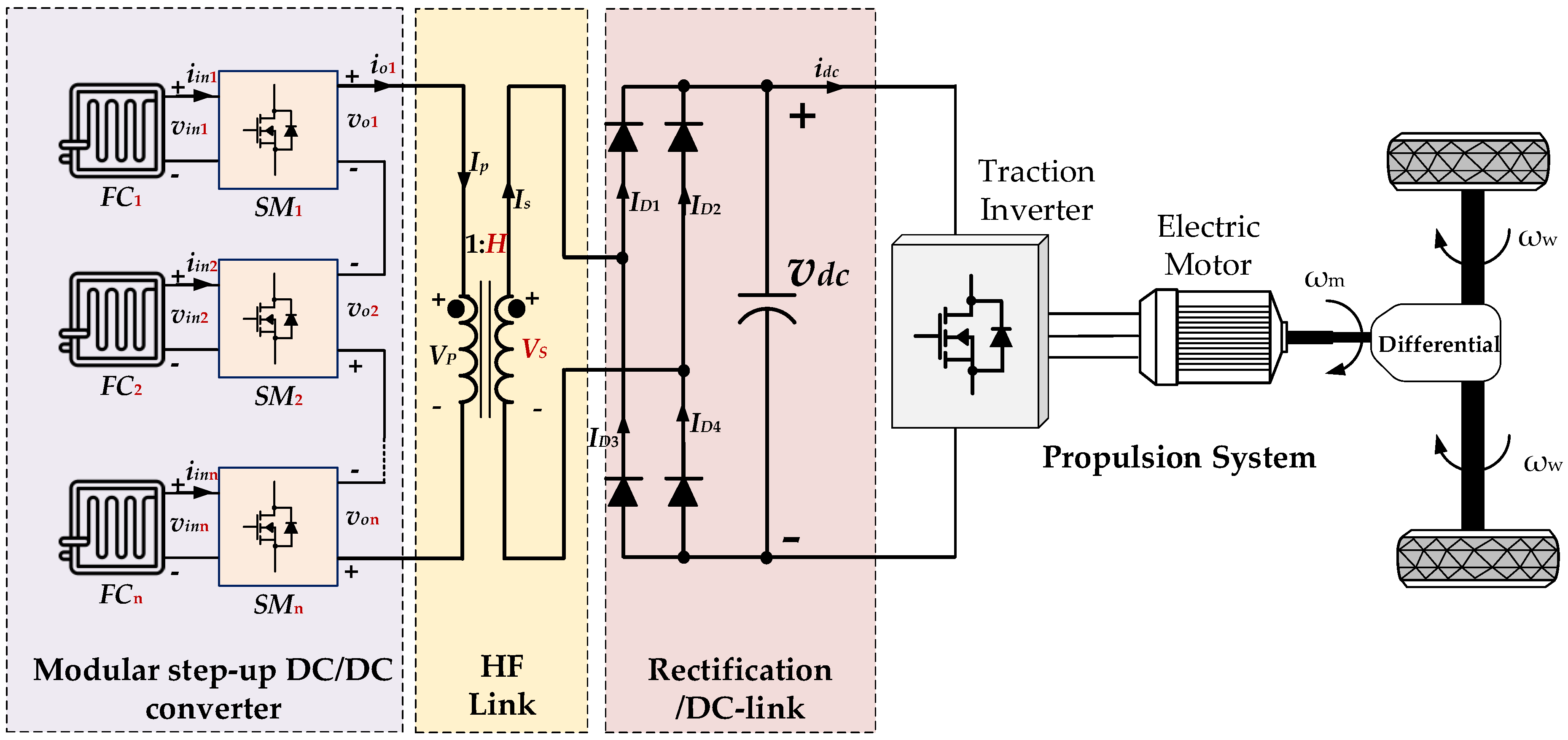
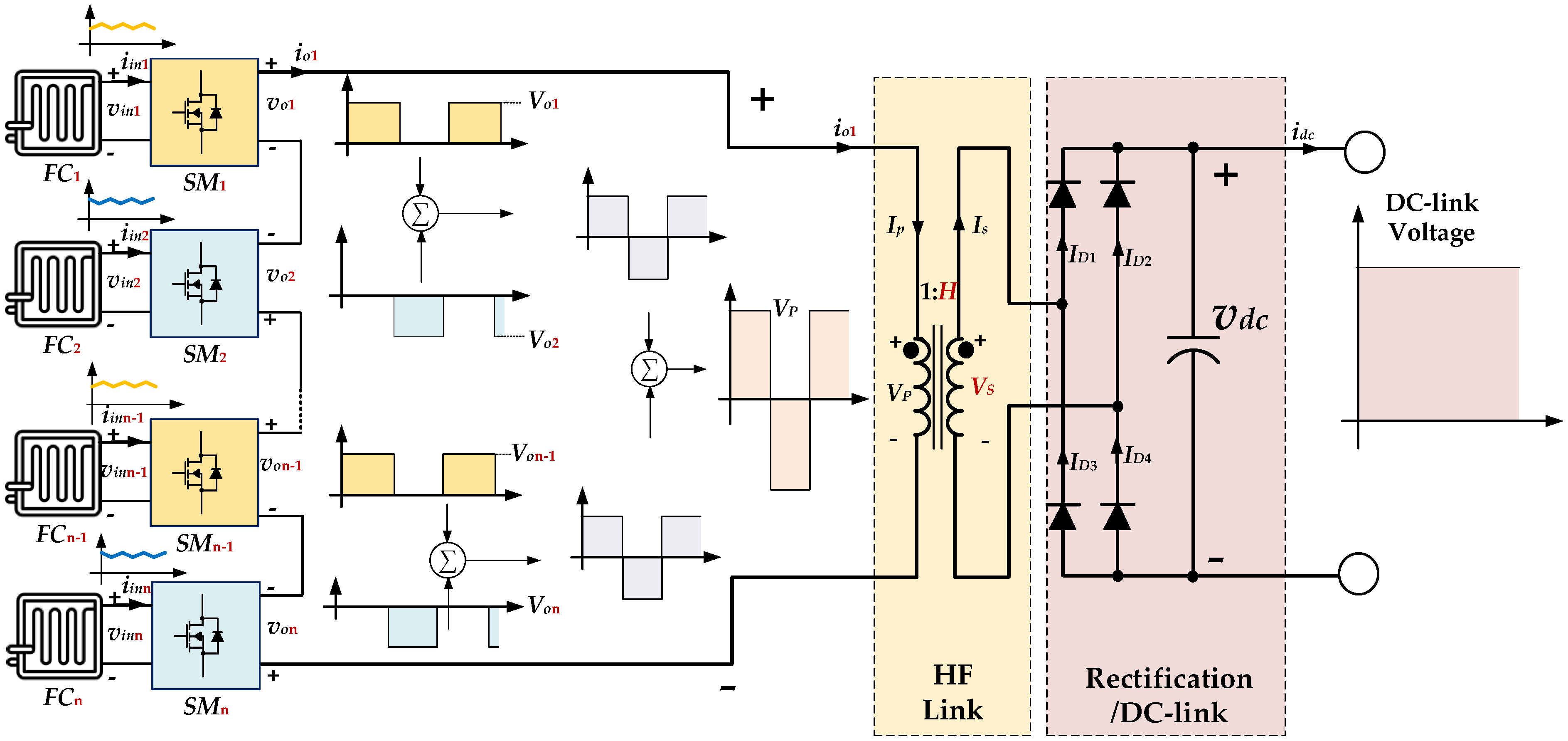
2. System Description
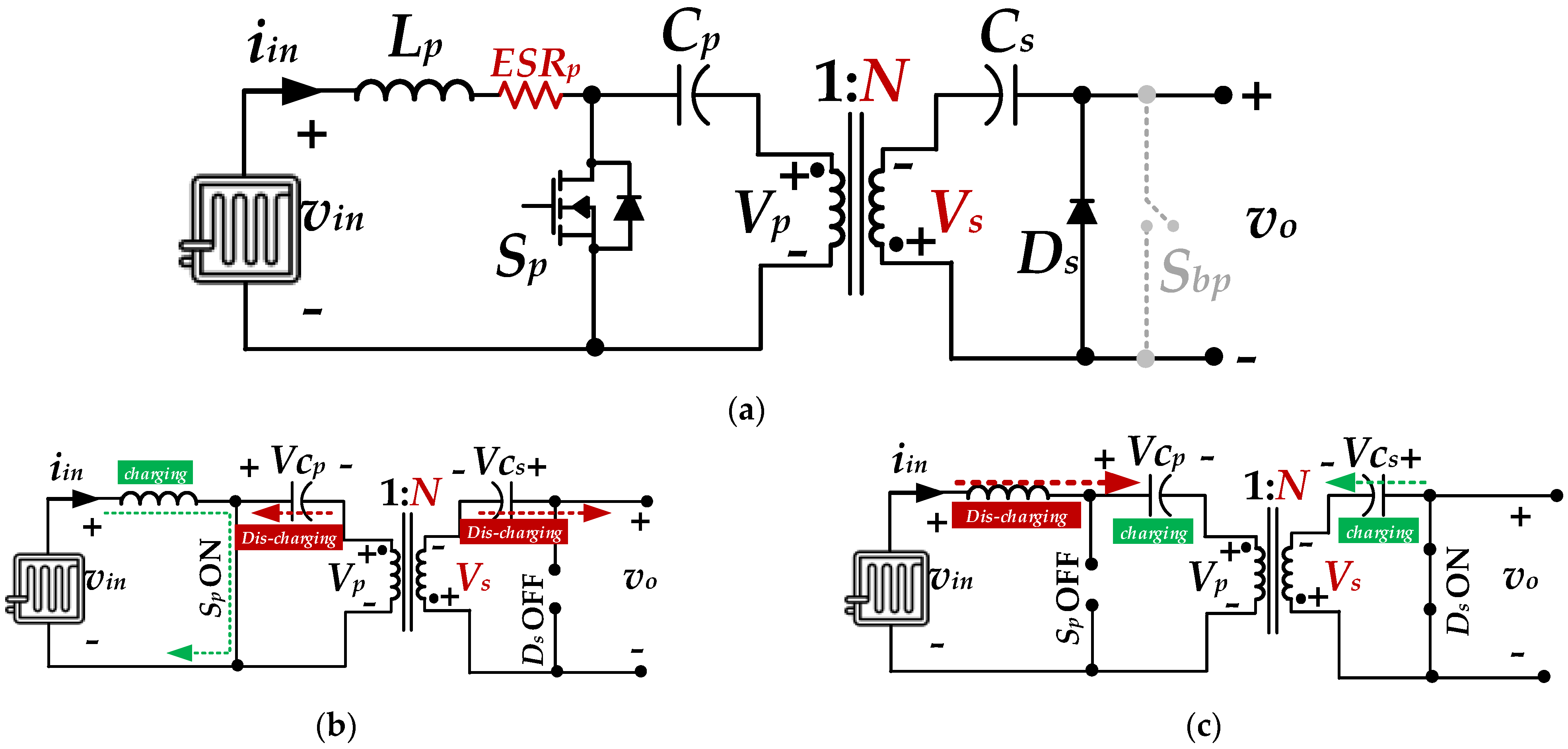
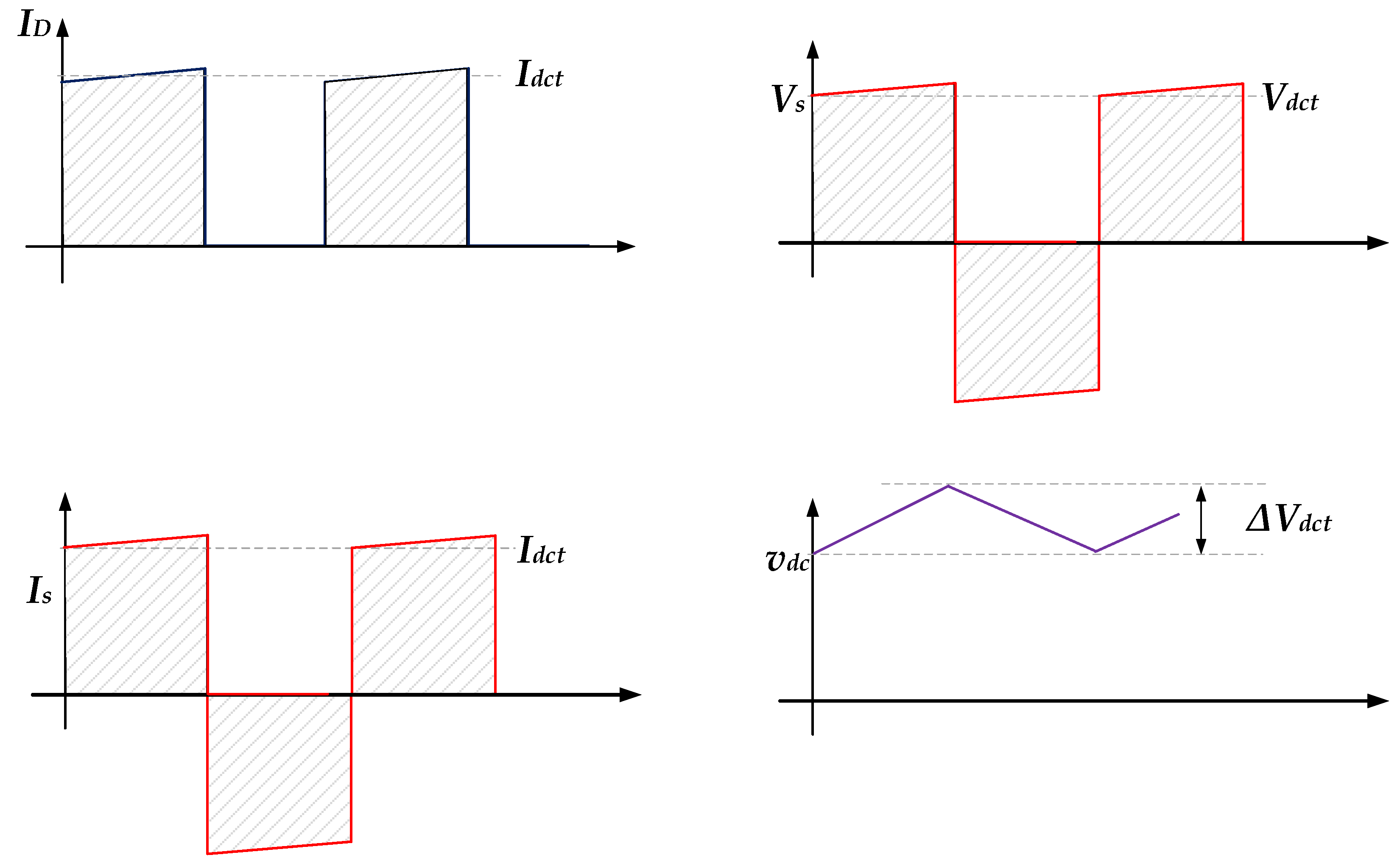
As shown in Figure 2, the output terminals of the individual SMs are connected in series differentially to collect the output voltages. The output voltages of each two successive SMs are controlled to be complimentary to each other by controlling the duty cycle ratios and the carrier signals of the pulse-width modulation (PWM) algorithm. This is to reduce the ripple of the total of these two voltages when added together and therefore the DC-link capacitance value can be reduced to save volume and weight inside the EV.
The output voltage of each two successive odd and even SMs forms a square wave with equal positive and negative peak values. These voltages are then added all together to form the input square voltage Vp to the primary side of the HFT. The stepped-up voltage at the secondary side of the HFT Vs is then rectified using the diode bridge followed by the DC-link capacitor Cdc. To show the basic operation of the system, the parameters in Table 1 are used in a SIMULINK/MATLAB model, and the computer simulation results are shown in Figure 3.
It should be noted that this computer simulation shows an ideal scenario as the FCs are assumed to have the same energy and the SMs are assumed to be identical. Figure 3a shows the input currents iin1 and iin2 of the first two successive SMs where carrier signals of the PMW algorithm for SM1 and SM2 have 180° phase shift. This shift means that the output voltages in Figure 3b are complimentary, which in turn reduces the voltage ripple of their summated voltage. Therefore, the total output voltage of the four SMs is continuous, as shown in Figure 3c.

3. SM Topology

The SM of the proposed modular step-up converter needs to have specific features in order to ensure that the overall operation is satisfying the required specifications. The selected SM must have the capability to boost the voltage of the FC to a higher voltage. Also, the SM must be suitable for isolation with HFTs to improve the voltage-boosting ratio. In addition, the SM should have a continuous input current with minimal current ripple to ensure that the efficiency of the FCs is not compromised. Indeed, it is desired that the selected SM has a low power loss to improve the efficiency of the total system. As the SM will be part of the bigger modular system, the controllability should be achievable with reasonable practical control schemes.
A good candidate for the proposed step-up DC/DC converter is the isolated SM shown in Figure 4. This SM is a modified version of the boost, Cuk, and Sepic converters designed to allow HFT isolation and the generation of a flexible boosted voltage at the output side while keeping the input current continuous. The key waveforms of the voltages and currents in the two successive SMs (SM1 and SM2) are shown in Figure 5. The carrier signals of the PWM algorithm for each two successive SMs are set to be opposite to each other (i.e., up–down and down–up) to create a 180° phase shift in their output voltages. Due to the existence of the input inductor Lp, the input current drawn from the power source is continuous in nature. The existence of the middle capacitors Cp and Cs blocks the DC currents flowing into the SM HFT and therefore the voltages across the primary and secondary sides of the transformer maintain the voltage-second balance. Accordingly, the saturation of the core is avoided. The output voltages of the two SMs are equal and shifted by 180° ready to be collected by the main HFT. The bypass switch Sbp at the output side is inserted to bypass the SM in case of any fault in the switch Sp, the diode Ds, or any other passive component. As Sbp is not expected to operate usually, a slow semiconductor switch or even a single-pole–single-throw (SPST) relay can be selected.
During normal operation, the sweet spot for the operation occurs at d1 = d2 = 0.5, where the two output voltages vo1 and vo2 are out of phase and therefore the output voltage ripples are minimized. Analysing SM1, the average voltages of the capacitors Cp1 and Cs1 can be expressed as
V c p 1 = v i n 1
V c s 1 = N d 1 1 d 1 v i n 1
The peak output voltage Vo1 is obtained from
V o 1 = N 1 d 1 v i n 1
For SM2, a similar analysis can be expressed as
V c p 2 = v i n 2
V c s 2 = N d 2 1 d 2 v i n 2
The peak output voltage Vo2 is obtained from
V o 2 = N 1 d 2 v i n 2
The total DC-link voltage can be obtained from
v D C = i = 1 n d i N 1 d i v i n i
In the ideal scenario when the input voltages of the fuel cell stacks are equal to Vin and hence the system operates with identical duty cycle ratios D = 0.5 for all SMs, the DC-link voltage can be expressed as
v D C _ e = n N H 2 V i n
It should be noted that the system operates at this nominal D = 0.5 when all SMs are healthy and operating at equal or close input voltages. However, there may be cases where some of the SMs are out of service, either deliberately or due to an unplanned fault. In this case, the faulty SMs can be bypassed by their output switches Sbp and the individual duty cycle ratios for the unfaulty SMs can be increased to compensate for the voltage lost by the faulty SMs. Figure 6 shows the case when a fault occurs in the input switches of the bottom two SMs at t = 0.1 s. Figure 6a shows the duty cycle ratios of the four SMs where d1 and d2 are increased from 0.5 to 0.75 to compensate for losing 200 V from SM3 and SM4 and keep the DC-link voltage at 400 V. The top graph of Figure 6b shows the primary voltage Vp of the main HFT while the bottom graph shows a zoomed-in figure of Vp after the fault. Figure 6c shows the DC-link voltage. As the duty cycle ratios of SM1 and SM2 are increased above 0.5, the ripple voltage across the DC-link capacitor is increased. This ripple voltage can be reduced by either increasing the DC-link capacitor voltage or by increasing the switching frequency of the SMs during faults.

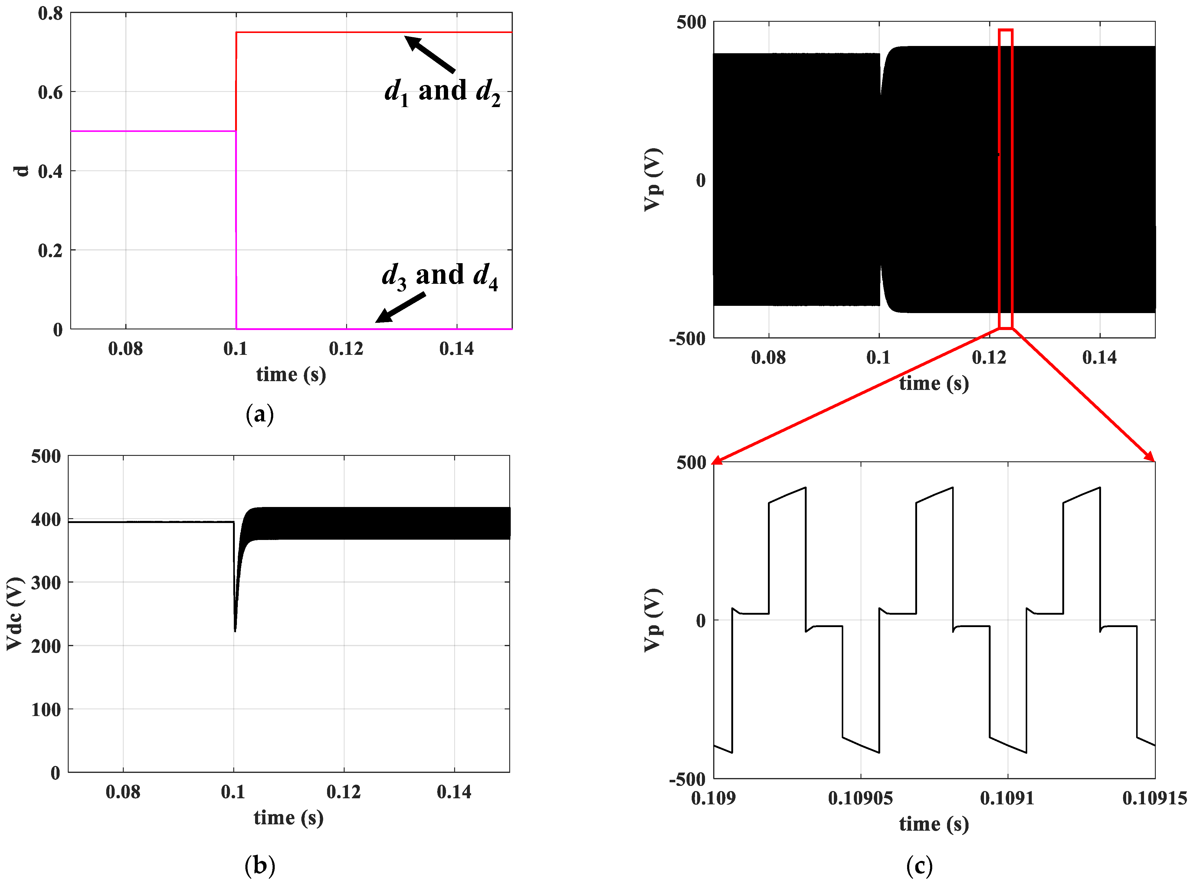
4. Computer Simulations

This section illustrates the operation of the proposed step-up isolated DC/DC converter in the SIMULINK/MATLAB model. The output of the converter is connected to the DC link of the EV propulsion system which controls the electric motor. The main parameters of the propulsion system are listed in Table 2.

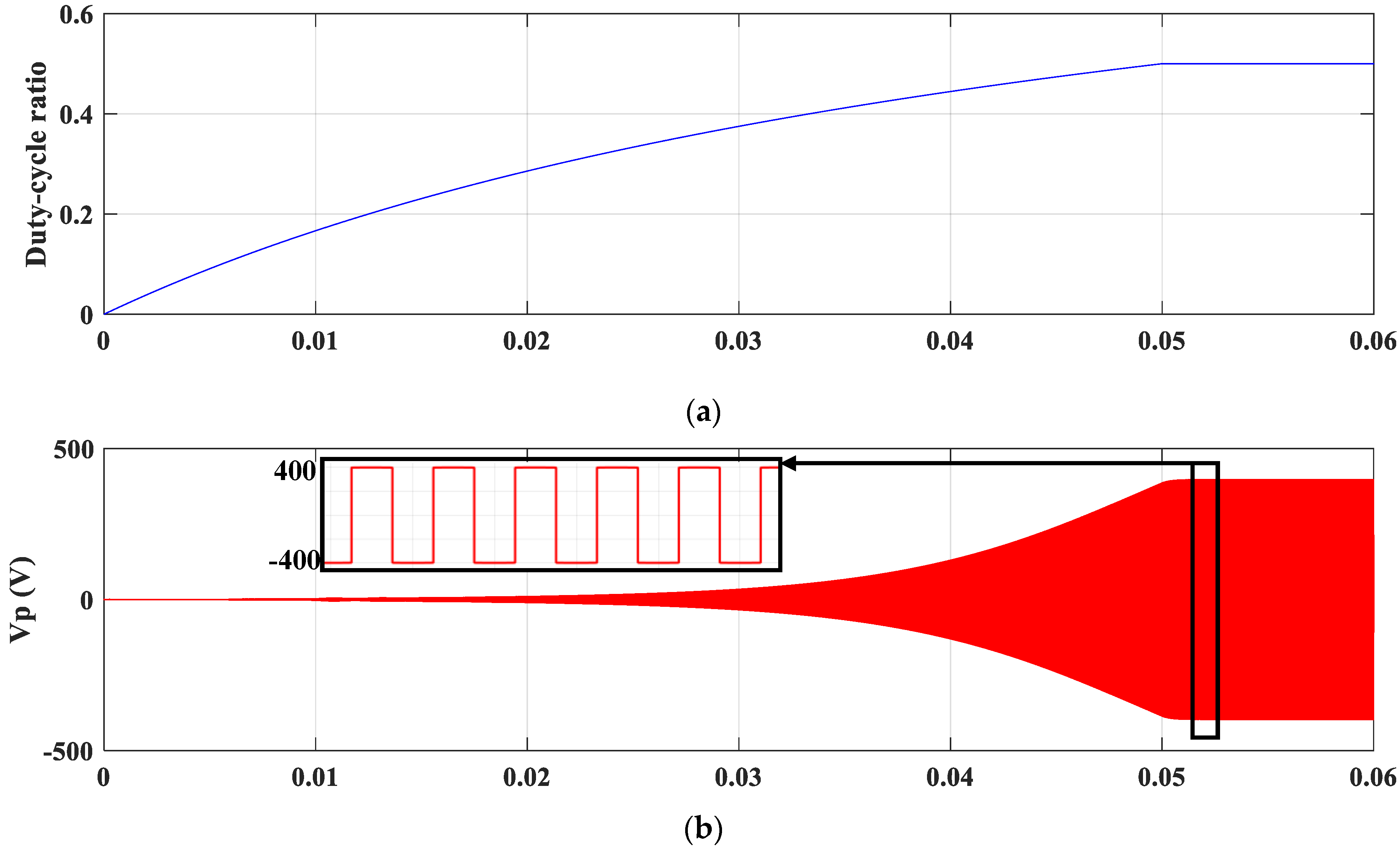
4.1. Warming Up (Building the DC-Link Voltage)

Figure 7 shows the output voltage of the step-up DC/DC converter measured at the DC link during the initial stage in the system. The top graph shows the control duty cycle ratio of the SMs; the voltage is increased gradually over 50 ms to avoid large inrush currents. The middle graph shows the AC voltage at the primary side of the HFT. The bottom graph shows the building-up process of the output voltage Vdc, preparing it for the next stage. During this period, the input current from the FC sources is small because no power is generated at the motor side.

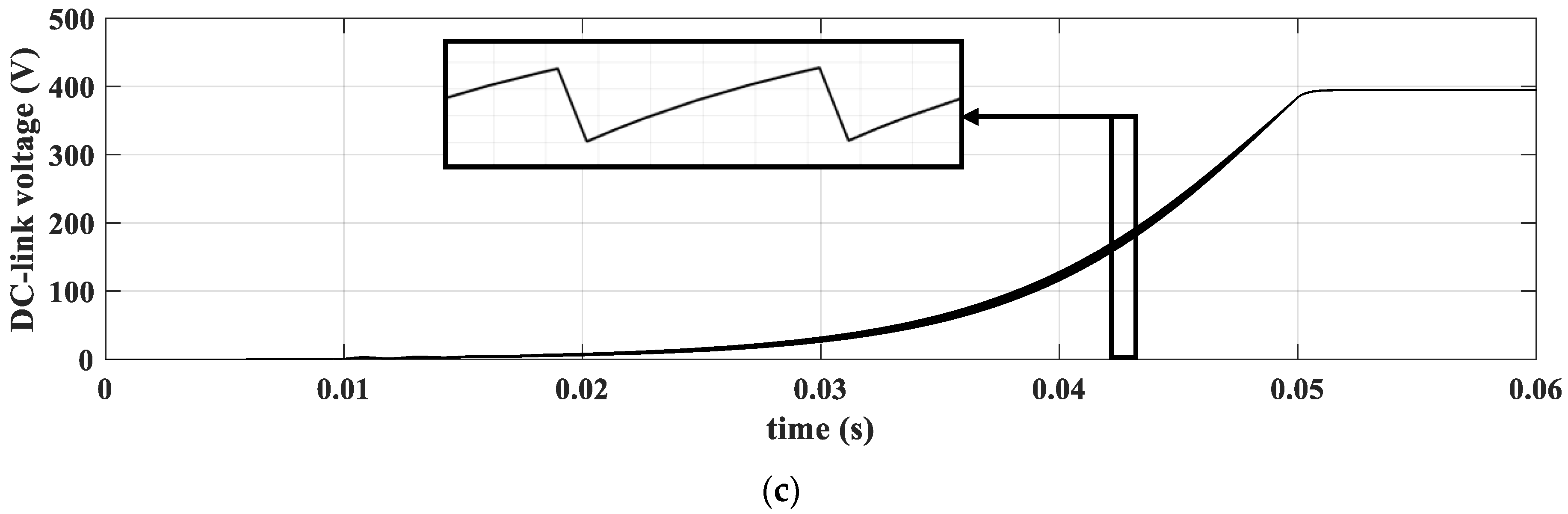
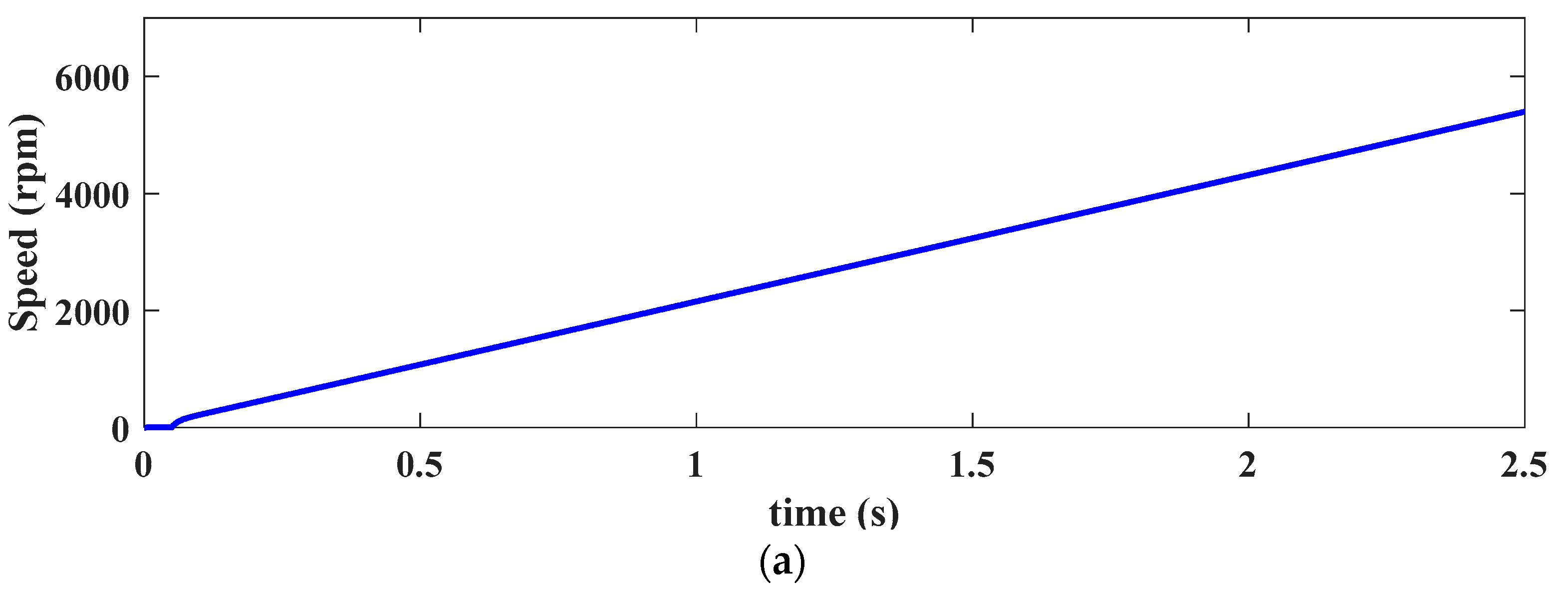
4.2. EV Acceleration

Figure 8 shows the performance of the drive system when the EV starts the normal operation. After the warming-up period is finished and the DC-link voltage reaches the required limit, the EV accelerates from zero to the maximum speed in 2.5 s. Figure 8a shows the speed of the electric motor when it increases from standstill to around 5800 revolutions per minute (rpm). To achieve this acceleration, the q-axis current of the electric motor is increased to around 78 A, as shown in Figure 8b, to provide the required torque for the EV. The mechanical power of the EV during the acceleration period is depicted in Figure 8c, which reaches around 90% of the peak power.
From the proposed converter’s perspective, it is desired to keep the DC-link voltage constant during this period to enable the drive inverter to provide high-efficiency operation and control of the electric motor. Figure 9 shows the parameters of the DC link and its associated components such as the rectifier and the HFT. Figure 9a shows the DC-link voltage during the acceleration period where the controller is keeping it at the desired nominal value (Vdc = 400 V). Meanwhile, the voltage at the primary side of the HFT Vp is a square wave with peak voltages of ±Vdc, as shown in Figure 9b. The current flowing into the primary side of this HFT is shown in Figure 9c.
The computer simulation model is built with identical SMs with the same semiconductor devices as well as passive elements. Also, the input voltages to these SMs are all equal. This means that the voltage and current waveforms inside the SMs will be identical to each other and therefore the results will be shown only for the first SM. Figure 10a shows the input current of the first SM iin1 where it increases with time because the power absorbed from the energy sources is increasing gradually to satisfy the mechanical power requested by the propulsion system. Figure 10b shows the current flowing into the input switch of the SM, which is important when designing SMs. Figure 10c shows the current flowing into the rectifier circuit’s diodes Id1, which is then rectified by the DC-link capacitor Cdc. Finally, Figure 10d shows the DC-link output current which is absorbed by the propulsion inverter of the EV.

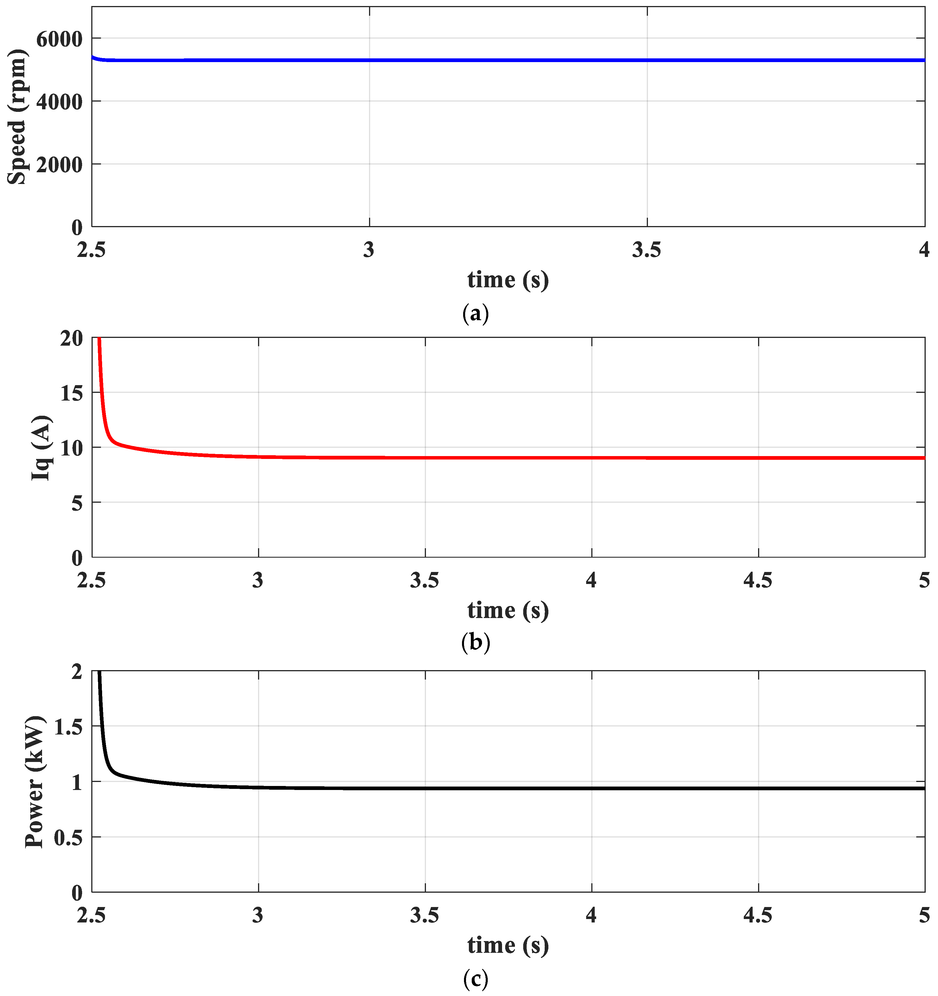
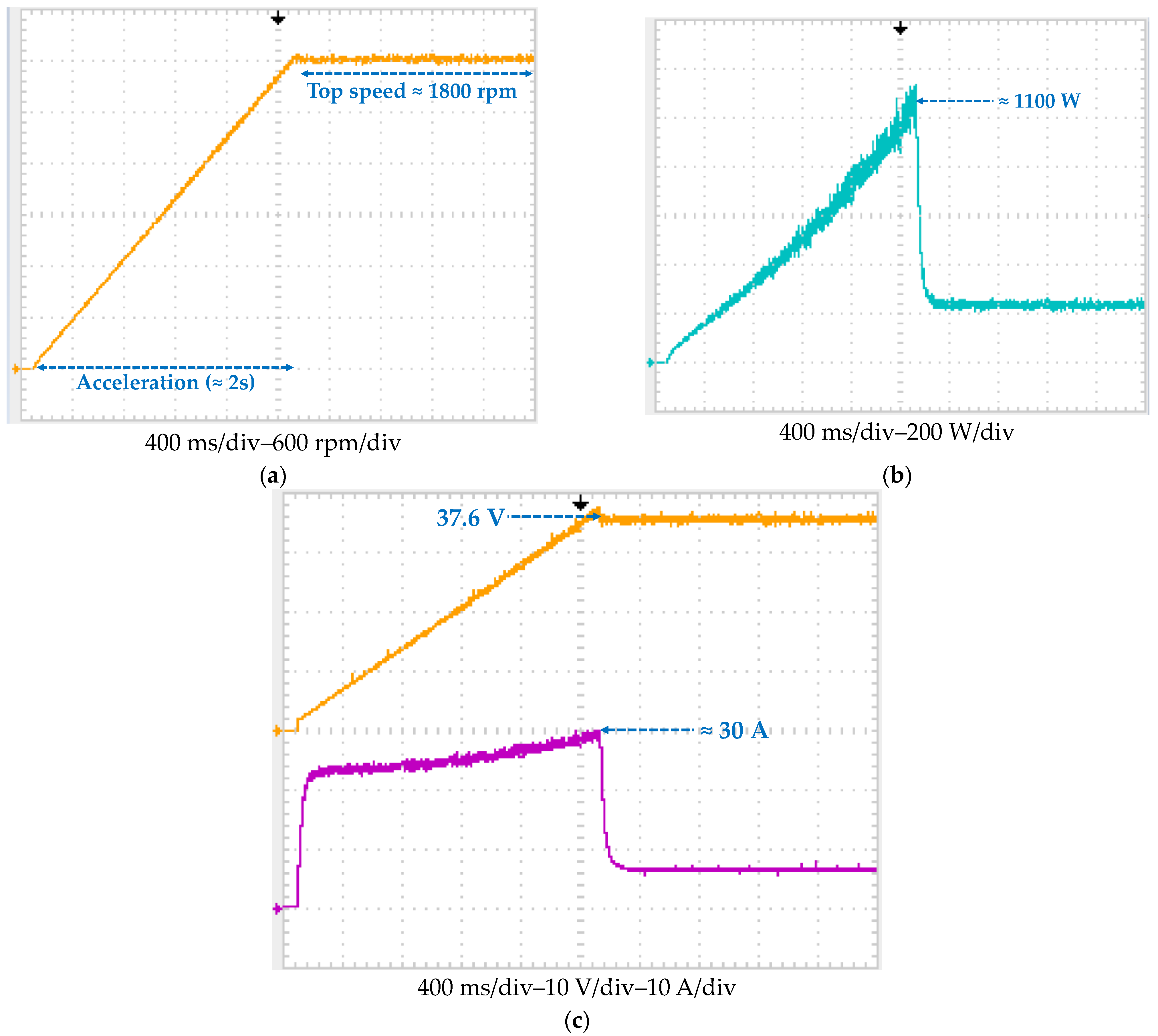
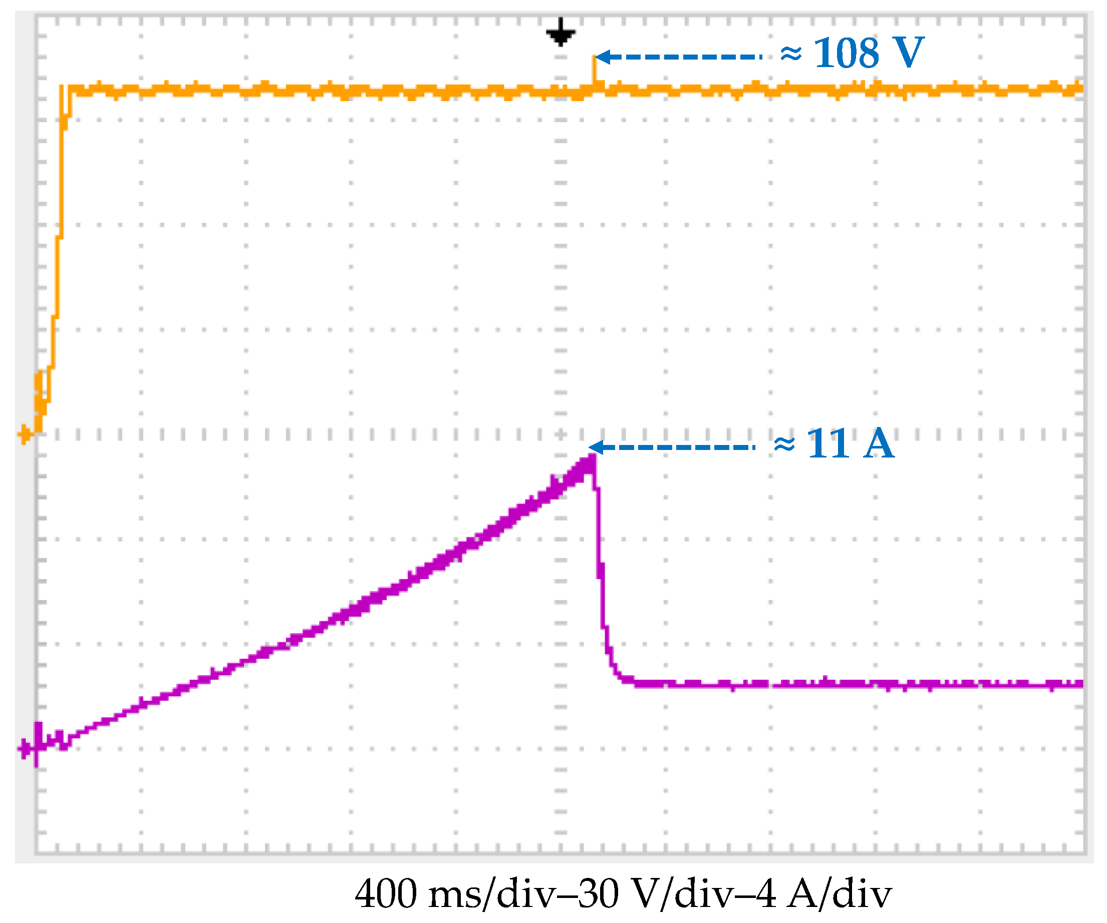
4.3. EV Top-Speed Operation

Once the top speed is reached, the absorbed current by the electric motor drops significantly as high torque is no longer needed. This leads to a significant drop in the power which reduces the currents of the FC sources, DC link, and the drive system. Figure 11 shows the performance of the drive system when the EV reaches the top speed after the acceleration period is finished. Figure 11a shows the speed of the electric motor. The q-axis current of the PMSM in Figure 11b drops to around 9 A, which is equivalent to the torque required to overcome the friction and air drag forces. The mechanical power of the EV during the acceleration period is depicted in Figure 11c, which falls to around 10% of the peak power. Figure 12a shows that the input current of the first SM iin1 is constant with time because the propulsion system of the EV draws constant power from the energy sources. Figure 12b shows the current flowing into the input switch of the SM. Figure 12c shows the current flowing into the rectifier circuit’s diodes Id1 which is then rectified by the DC-link capacitor Cdc. Finally, Figure 12d shows the DC-link output current which is absorbed by the propulsion inverter of the EV.

5. Parameter Design

As the final goal of the proposed step-up DC/DC converter is to provide the EV propulsion system with electrical energy, the design process should start with the propulsion system specifications.

5.1. EV Propulsion Mechanical Specifications

Assuming the wheel’s radius (r) is known and constant, the relation between the linear speed of the EV (v) and the rotational velocity of the wheels ωw can be obtained from
v = ω w r
As the top-speed vt of the EV is one of its design specifications, the top angular speed is
ω w t = v t r
The total force of the EV is a summation of the rolling resistance force (Fr), the air drag resistance force (Fad), the acceleration force (Fa), and any hill-climbing force (Fhc). This total force can be expressed as
F t = F r + F a d + 1.05 F a c c + F h c
F t = μ r m g + 1 2 ρ A C d v 2 + 1.05 m a + m g s i n α
where m is the vehicle’s mass, μr is the coefficient of rolling resistance, ρ is the density of the air, A is the frontal area, a is the vehicle’s linear acceleration, and Cd is the drag coefficient. The total torques required by the four wheels (Tw) and the torque required to be generated by the motor (Tm) are calculated from
T w = F t r
T m = T w η g G
where ηg and G are the efficiency and the gear’s ratio of the mechanical differential, respectively. It should be noted that the maximum torque at the wheels and motor will be generated during the acceleration period of the EV. Thus, the peak values of Tw and accordingly Tm should be calculated from (11)–(14) during acceleration and used as the targeted design specifications with the acceleration value a. The maximum angular speed of the motor’s rotor is calculated from
ω m t = G ω w t
The maximum mechanical power consumed by the EV is then calculated from
P m t = T m ω m t
The maximum electrical power supplied by the DC link is
P e t = P m t η m η d
where ηm and ηd are the efficiencies of the motor and the drive inverter, respectively. Figure 13 shows a summary of the main waveforms used in choosing the mechanical specifications.

5.2. DC-Link Design Specifications

The current supplied by the DC link to the drive inverter is calculated from the electrical power of the propulsion system in (17) and the controlled DC-link voltage which is controlled by the SMs and the main HFT. A typical value of this voltage in the present EV propulsion systems is in the range 400 V to 800 V. Increasing the DC-link voltage enables the drive inverter, and hence the electric motor, to operate at higher speed without the necessity for increasing G significantly and therefore high-power levels can be reached. However, increasing the DC-link voltage beyond 400 V creates safety issues for the users. In general, most of the EV manufacturers are moving toward higher DC-link voltages. The design value of the DC-link current should match the highest possible current which occurs at the end of the acceleration period. This value is obtained from
I d c t = P e t V d c
The peak current flowing in the diodes of the rectifier circuit as well as the main HFT should be used in designing these elements, as shown in Figure 14.
The value of the DC-link capacitor Cdc is chosen to reduce the maximum permitted ripple voltage in the DC-link ΔVdc (see Figure 14). This can be obtained from
C d c = I d c t 2 f s V d c

5.3. SM Design Specifications

The number of SMs in the system is determined by the minimum expected input voltage from the energy sources, the desired DC-link voltage, and the turn ratio of the internal and main HFTs. This can be expressed as
n = 2 v D C _ e N H V i n
According to the selected n and N, the peak value of the output voltage of the SM (Vo) becomes
V o = 2 N V i n
Therefore, the peak voltage seen by the semiconductor devices inside the SM can be calculated from
V d e v i c e = V o
The maximum value of the SM input current can be obtained from the maximum power calculation mentioned earlier in (17) as
I i n _ p e a k = P e t n η S M V i n
As the information on SMs’ efficiency (ηSM) is not available before the design process, it can be assumed that it is of a low value (i.e., in the range of 90%) to ensure a safer design for the semiconductor switches. The peak current flowing in the primary side switch of the SM is then calculated from
I S p _ p e a k = 2 I i n _ p e a k

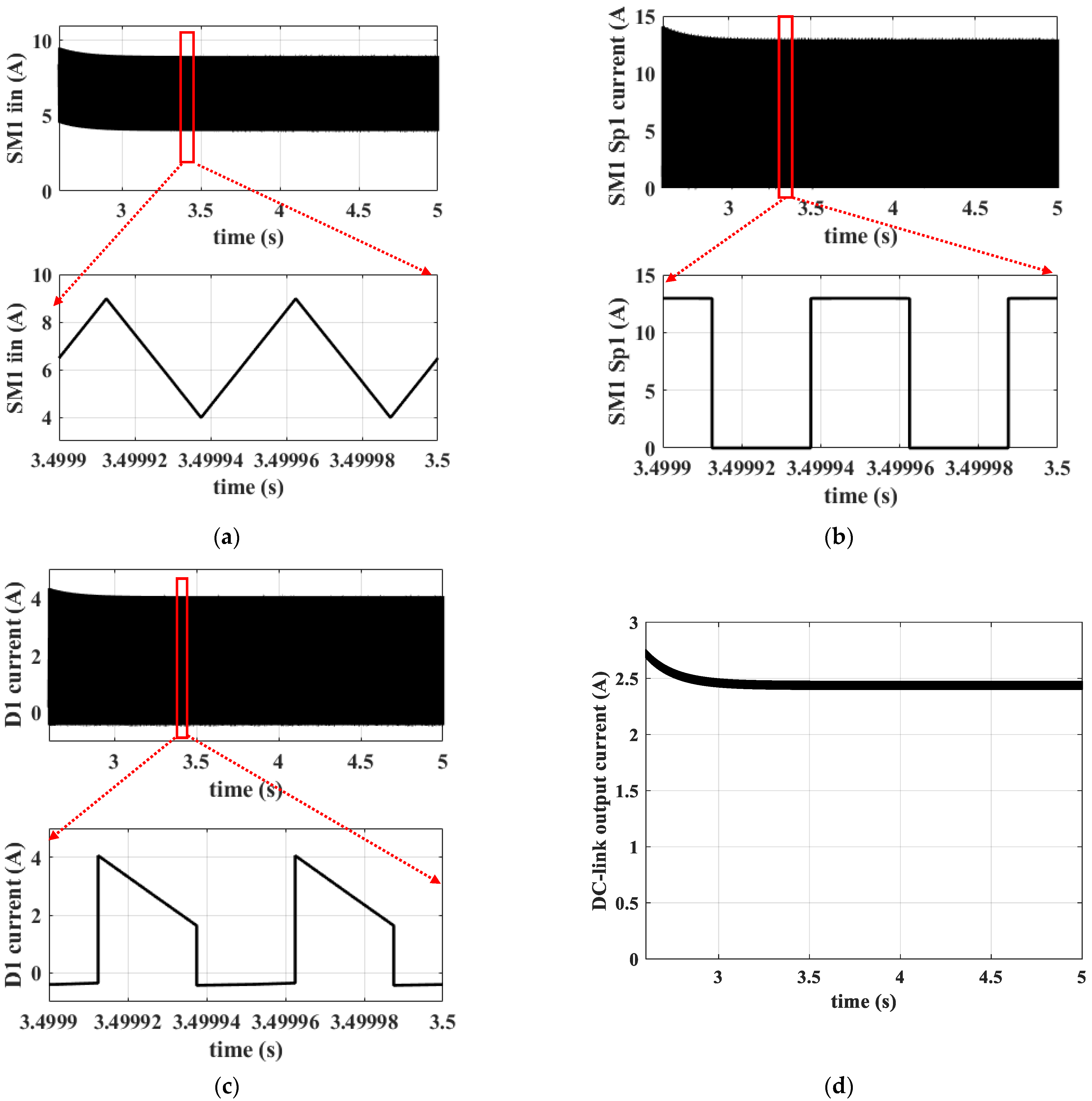
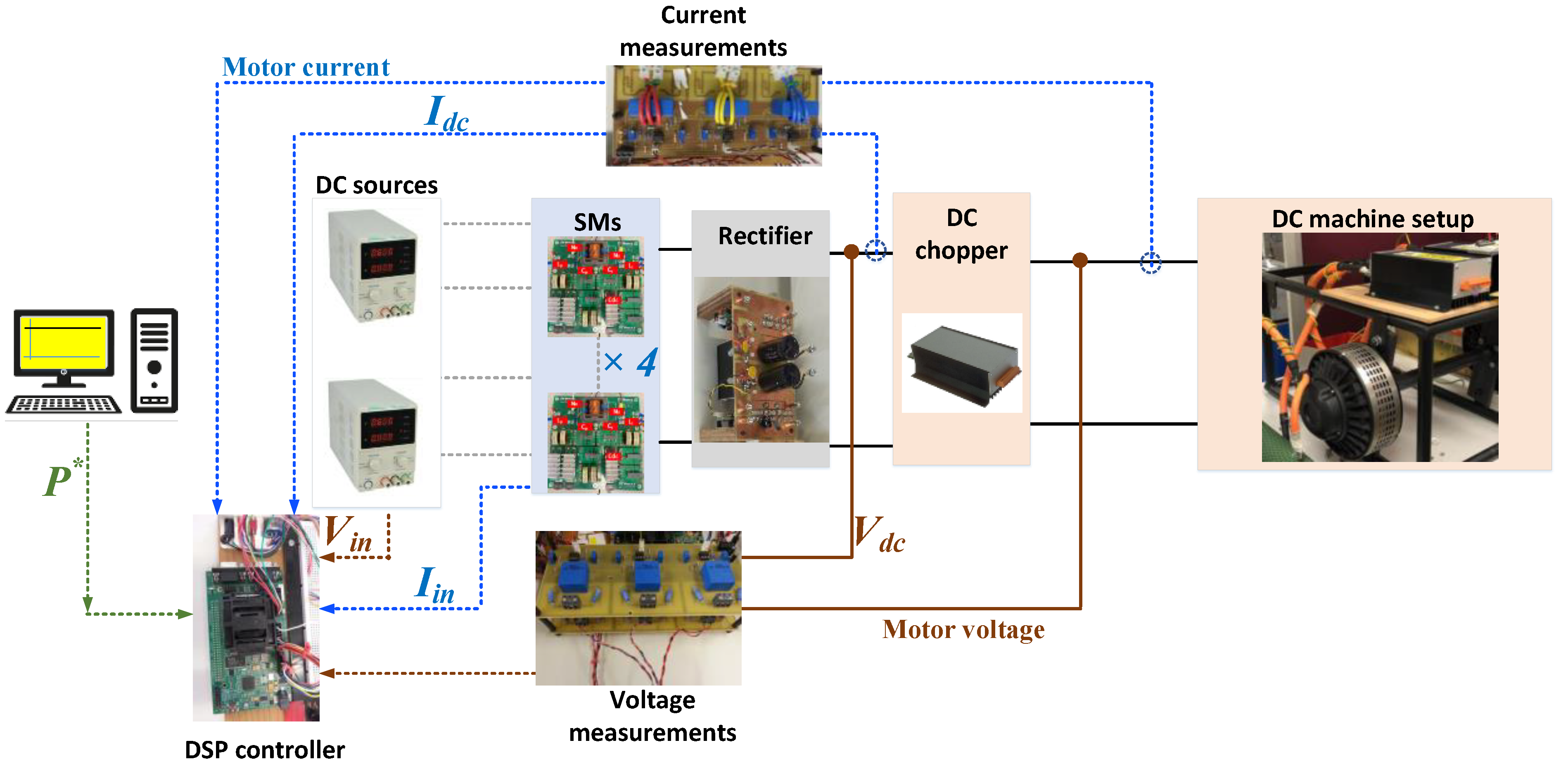
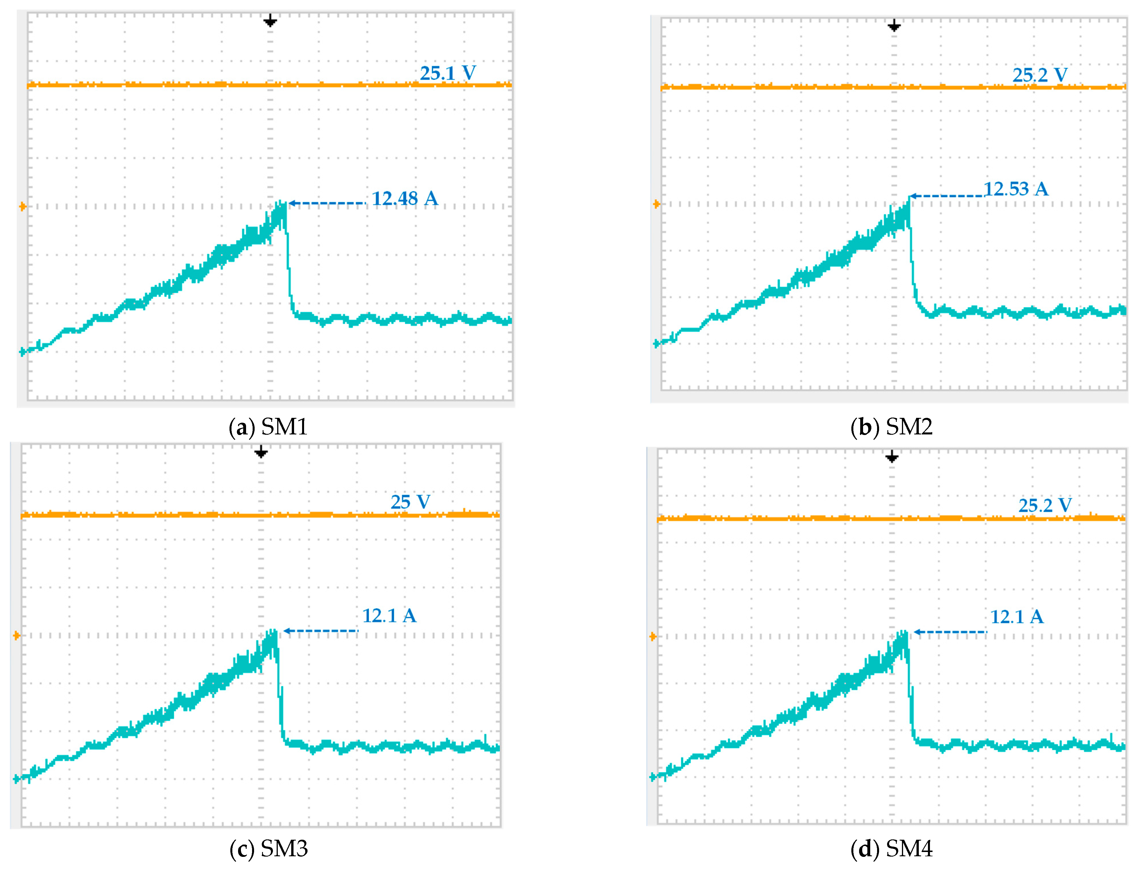
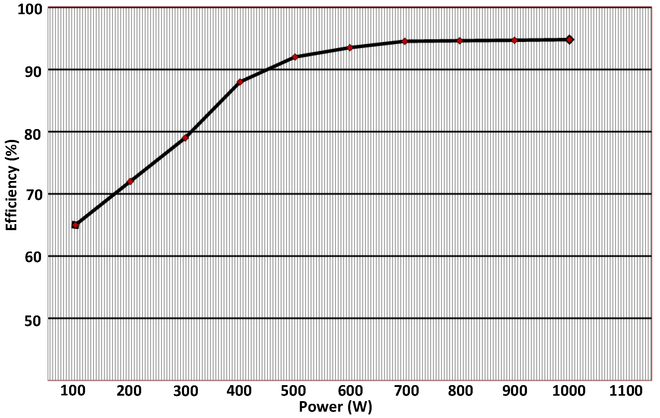
6. Experimental Results

A small-scale prototype is prepared to test the feasibility of the proposed modular step-up converter with an electrical machine, as shown in Figure 15. The main parameters of the test rig are listed in Table 3 where the total nominal power is 1 kW. The system is controlled by a TMS320F28335 digital signal processor (DSP) controller which receives the voltage and current measurements from the converter’s sensors.
Figure 16 shows the main waveforms of the electric motor supplied by the proposed step-up DC/DC converter. The rotational speed of the motor is shown in Figure 16a when the system accelerates from standstill to around 1800 rpm in 2 seconds. Figure 16b shows the mechanical power while Figure 16c shows the machine’s voltage and current.
Figure 17 shows the DC-link voltage and current during the whole process. The maximum voltage overshoot across the DC link during the transition from acceleration to top-speed operation is 8%, which can be reduced by increasing the DC-link capacitance value. Finally, the input voltages of the four SMs as well as the currents are shown Figure 18. The efficiency of the system at steady state can be estimated from the voltages and currents generated in Figure 17 and Figure 18 to be approximately 95%. The efficiency is expected to increase when increasing the operational power of the small-scale prototype.
Figure 19 shows the increase in efficiency when increasing the power drawn from the power sources. This is mainly due to the increased ratio of the output power to the fixed losses including the gate drivers’ power losses, switching losses in the semiconductor devices, and magnetizing losses in the transformer cores, either in the SMs or before the DC link. Figure 20 shows a comparison between the proposed converter and other common topologies in terms of their features on a scale of 1–3. The proposed converter is superior in its low input ripple current, low device count, providing isolation, and its scalability when more SMs are needed. Other converters may be favourable due to better efficiency or the simplicity of their circuits.

7. Conclusions

The proposed modular step-up DC/DC converter is well suited to EV applications where input energy sources must be connected separately due to differences in their types or voltage ranges. The converter efficiently harvests electrical energy from these sources and builds the DC-link voltage by summing the output voltages of each SM in the system. Since each SM is designed as an isolated DC/DC converter, its output voltage can be boosted using an HFT. To achieve an additional degree of voltage boosting, the total output voltages of the SMs are controlled to form a high-frequency square wave, enabling the use of an HF link transformer before the rectification process. The feasibility of the proposed converter is demonstrated through MATLAB/Simulink simulations and experimental results, which show that system efficiency can exceed 95%. The voltage gain of the proposed converter is 1:8, and this can be increased by increasing the number of SMs or by increasing the HFT turns’ ratio. Another notable feature observed in both simulations and experiments is the significant reduction in DC-link capacitance when the duty cycle of the SMs is maintained close to 50%. A DC-link capacitor of less than 100 µF was used in both simulations and experiments and kept the ripple voltage below 10% and the voltage overshoot during transition from acceleration to top-speed operation below 8%. Simulations using MATLAB/Simulink (with a PMSM load) and experimental results (with a brushed DC motor) confirm that the loading of the EV propulsion system has minimal impact on the front-end performance of the proposed modular step-up DC/DC converter. However, it should be noted that modular converters, by their nature, are more complex to control compared to centralized converters. Therefore, a detailed control scheme must be addressed in future publications to manage this complexity effectively.

Funding

This research received no external funding.

Data Availability Statement

The original contributions presented in the study are included in the article, further inquiries can be directed to the author.

Conflicts of Interest

The author declares no conflicts of interest.

References

  1. Zeng, B.; Zhang, J.; Yang, X.; Wang, J.; Dong, J.; Zhang, Y. Integrated planning for transition to low-carbon distribution system with renewable energy generation and demand response. IEEE Trans. Power Syst. 2013, 29, 1153–1165. [Google Scholar] [CrossRef]
  2. Zhang, Y.; Liu, H.; Li, J.; Sumner, M.; Xia, C. DC–DC Boost Converter with a Wide Input Range and High Voltage Gain for Fuel Cell Vehicles. IEEE Trans. Power Electron. 2019, 34, 4100–4111. [Google Scholar] [CrossRef]
  3. Aljumah, A.; Darwish, A.; Csala, D.; Twigg, P. A Review on the Allocation of Sustainable Distributed Generators with Electric Vehicle Charging Stations. Sustainability 2024, 16, 6353. [Google Scholar] [CrossRef]
  4. IEA. Global EV Outlook 2023: Catching Up with Climate Ambitions. 2023. Available online: https://iea.blob.core.windows.net/assets/dacf14d2-eabc-498a-8263-9f97fd5dc327/GEVO2023.pdf (accessed on 1 January 2024).
  5. Bi, H.; Wang, P.; Che, Y. A capacitor clamped H-type boost DC-DC converter with wide voltage-gain range for fuel cell vehicles. IEEE Trans. Veh. Technol. 2019, 68, 276–290. [Google Scholar] [CrossRef]
  6. Wang, P.; Zhou, L.; Zhang, Y.; Li, J.; Sumner, M. Input-Parallel Output-Series DC-DC Boost Converter with a Wide Input Voltage Range, For Fuel Cell Vehicles. IEEE Trans. Veh. Technol. 2017, 66, 7771–7781. [Google Scholar] [CrossRef]
  7. Bakar, M.; Alam, M.; Wårdemark, M.; Bertilsson, K. A 2 × 3 Reconfigurable Modes Wide Input Wide Output Range DC-DC Power Converter. IEEE Access 2021, 9, 44292–44303. [Google Scholar] [CrossRef]
  8. Benites Quispe, J.B.; Mezaroba, M.; Batschauer, A.L.; de Souza Ribeiro, J.M. A Reconfigurable Phase-Shifted Full-Bridge DC–DC Converter with Wide Range Output Voltage. Energies 2024, 17, 3483. [Google Scholar] [CrossRef]
  9. de Sá, F.L.; Ruiz-Caballero, D.; Dal’Agnol, C.; da Silva, W.R.; Mussa, S.A. High Static Gain DC–DC Double Boost Quadratic Converter. Energies 2023, 16, 6362. [Google Scholar] [CrossRef]
  10. Zhang, Y.; Sumner, L.Z.M.; Wang, P. Single-Switch, Wide Voltage-Gain Range, Boost DC–DC Converter for Fuel Cell Vehicles. IEEE Trans. Veh. Technol. 2018, 67, 134–145. [Google Scholar] [CrossRef]
  11. Alotaibi, S.; Ma, X.; Darwish, A. Dual Isolated Multilevel Modular Inverter with Novel Switching and Voltage Stress Suppression. Energies 2022, 15, 5025. [Google Scholar] [CrossRef]
  12. Elgenedy, M.A.; Darwish, A.; Ahmed, S.; Williams, B.W. A Modular Multilevel-Based High-Voltage Pulse Generator for Water Disinfection Applications. IEEE Trans. Plasma Sci. 2016, 44, 2893–2900. [Google Scholar] [CrossRef]
  13. Darwish, A.; Holliday, D.; Finney, S. Operation and control design of an input-series–input-parallel–output-series conversion scheme for offshore DC wind systems. IET Power Electron. 2017, 10, 2092–2103. [Google Scholar] [CrossRef]
  14. Darwish, A.; Massoud, A.; Holliday, D.; Ahmed, S.; Williams, B. Generation, performance evaluation and control design of single-phase differential-mode buck–boost current-source inverters. IET Renew. Power Gener. 2016, 10, 916–927. [Google Scholar] [CrossRef]
  15. Darwish, A.; Elserougi, A.; Abdel-Khalik, A.S.; Ahmed, S.; Massoud, A.; Holliday, D.; Williams, B.W. A single-stage three-phase DC/AC inverter based on Cuk converter for PV application. In Proceedings of the 2013 7th IEEE GCC Conference and Exhibition (GCC), Doha, Qatar, 17–20 November 2013; pp. 384–389. [Google Scholar]
  16. Leyva-Ramos, J.; Ortiz-Lopez, M.G.; Diaz-Saldierna, L.H.; Morales-Saldana, J.A. Switching regulator using a quadratic boost converter for wide dc conversion ratios. IET Power Electron. 2009, 2, 605–613. [Google Scholar] [CrossRef]
  17. Axelrod, B.; Berkovich, Y.; Ioinovici, A. Switched-capacitor/switched-inductor structures for getting transformerless hybrid dc–dc PWM converters. IEEE Trans. Circuits Syst. I Reg. Papers 2008, 55, 687–696. [Google Scholar] [CrossRef]
  18. Maalandish, M.; Hosseini, S.H.; Jalilzadeh, T. High step-up dc/dc converter using switch-capacitor techniques and lower losses for renewable energy applications. IET Power. Electron. 2018, 11, 1718–1729. [Google Scholar] [CrossRef]
  19. Tang, Y.; Wang, T.; He, Y. A Switched-Capacitor-Based Active-Network. IEEE Trans. Power Electron. 2014, 29, 2959–2968. [Google Scholar] [CrossRef]
  20. Pires, V.F.; Cordeiro, A.; Foito, D.; Silva, J.F. High Step-Up DC-DC Converter for Fuel Cell Vehicles Based on Merged Quadratic Boost-Ćuk. IEEE Trans. Veh. Technol. 2019, 68, 7521–7530. [Google Scholar] [CrossRef]
  21. Wang, Y.; Qiu, Y.; Bian, Q.; Guan, Y.; Xu, D. A Single Switch Quadratic Boost High Step Up DC–DC Converter. IEEE Trans. Ind. Electron. 2019, 66, 4387–4397. [Google Scholar] [CrossRef]
  22. Wu, X.; Yang, M.; Zhou, M.; Zhang, Y.; Fu, J. A novel high-gain dc-dc converter applied in fuel cell vehicles. IEEE Trans. Veh. Technol. 2020, 69, 12763–12774. [Google Scholar] [CrossRef]
  23. Vettuparambil, A.; Chatterjee, K.; Fernandes, B.G. Dual-active-bridge-based multiport converter with split DC links. IEEE Trans. Ind. Electron. 2022, 69, 485–494. [Google Scholar] [CrossRef]
  24. Vettuparambil, A.; Chatterjee, K.; Fernandes, B.G. A Multiport Converter Interfacing Solar Photovoltaic Modules and Energy Storage with DC Microgrid. IEEE Trans. Ind. Electron. 2021, 68, 3113–3123. [Google Scholar] [CrossRef]
  25. Geng, Z.; Hong, T.; Qi, K.; Ambrosio, J.; Gu, D. Modular Regenerative Emulation System for DC–DC Converters in Hybrid Fuel Cell Vehicle Applications. IEEE Trans. Veh. Technol. 2018, 67, 9233–9240. [Google Scholar] [CrossRef]
  26. Krastev, I.; Tricoli, P. Boost multilevel cascade inverter for hydrogen fuel cell light railway vehicles. IEEE Trans. Ind. Electron. 2022, 69, 7837–7847. [Google Scholar] [CrossRef]
  27. Khalatbarisoltani, A.; Boulon, L.; Hu, X. Integrating model predictive control with federated reinforcement learning for decentralized energy management of fuel cell vehicles. IEEE Trans. Intell. Transport. Syst. 2023, 24, 13639–13653. [Google Scholar] [CrossRef]
  28. Benevieri, A.; Carbone, L.; Cosso, S.; Marchesoni, M.; Passalacqua, M.; Savio, S.; Vaccaro, L. A New Feed-Forward Control for Dynamics Improvement in a Dual-Input DC–DC Converter for Hybrid Vehicle Applications. Energies 2024, 17, 2170. [Google Scholar] [CrossRef]
  29. Ahmed, A.A.; Benmouna, A.; Becherif, M.; Hilairet, M.; Al-Sumaiti, A.S. New Interleaved-Input Double Float-Output DC/DC Converter Topology for Battery- Based EVs: Design, Modeling, Analysis and Experimental Implementation. IEEE Access 2024, 12, 77870–77890. [Google Scholar] [CrossRef]
  30. Darwish, A.; Elgenedy, M.A.; Williams, B.W. A Review of Modular Electrical Sub-Systems of Electric Vehicles. Energies 2024, 17, 3474. [Google Scholar] [CrossRef]
Figure 1. Basic circuit diagram of the proposed step-up DC/DC converter.
Energies 17 06305 g001
Figure 2. Operation of the modular step-up DC/DC converter.
Energies 17 06305 g002
Figure 3. MATLAB/SIMULINK simulation for the inputs and outputs of the proposed modular step-up DC/DC converter: (a) SM input current, (b) HFT primary voltage, and (c) DC-link voltage.
Energies 17 06305 g003
Figure 4. Voltage-boosting SM: (a) circuit schematic, (b) SM circuit when Sp is on, and (c) SM circuit when Sp is off.
Energies 17 06305 g004
Figure 5. Key waveforms of the voltages and currents in (a) SM1 and (b) SM2.
Energies 17 06305 g005
Figure 6. MATLAB/SIMULINK simulation during faults in SM3 and SM4: (a) SM duty cycle ratios, (b) DC-link voltage, and (c) HFT primary voltage.
Energies 17 06305 g006
Figure 7. Warming-up period: (a) duty cycle ratio, (b) HFT primary voltage, and (c) DC-link voltage.
Energies 17 06305 g007aEnergies 17 06305 g007b
Figure 8. EV propulsion system during acceleration: (a) motor speed, (b) motor Iq current, and (c) total mechanical power.
Energies 17 06305 g008aEnergies 17 06305 g008b
Figure 9. Waveforms of the DC link during acceleration: (a) DC-link voltage, (b) HFT primary side voltage, and (c) HFT primary side current.
Energies 17 06305 g009
Figure 10. SM1 current waveforms of the semiconductor devices during acceleration: (a) input current iiin1, (b) current through the primary side switch Sp1, (c) current through D1 diode in the rectifier circuit, and (d) DC/DC converter’s output current.
Energies 17 06305 g010
Figure 11. EV propulsion system during top-speed operation: (a) motor speed, (b) motor Iq current, and (c) total mechanical power.
Energies 17 06305 g011
Figure 12. SM1 current waveforms of the semiconductor devices during top-speed operation: (a) input current iiin1, (b) current through the primary side switch Sp1, (c) current through D1 diode in the rectifier circuit, and (d) DC/DC converter’s output current.
Energies 17 06305 g012
Figure 13. Sketches of the waveforms in the EV propulsion system.
Energies 17 06305 g013
Figure 14. Currents and voltages in the DC-link circuit.
Energies 17 06305 g014
Figure 15. Experimental setup description.
Energies 17 06305 g015
Figure 16. Main waveforms of the propulsion system: (a) motor speed in rpm, (b) input power, and (c) armature’s voltage (top) and current (bottom).
Energies 17 06305 g016
Figure 17. DC-link waveforms: DC-link voltage (top) and DC-link output current (bottom).
Energies 17 06305 g017
Figure 18. SM input voltages (top) and currents (bottom): 400 ms/div–10 V/div–4 A/div.
Energies 17 06305 g018
Figure 19. Efficiency of the proposed converter (without the traction inverter).
Energies 17 06305 g019
Figure 20. Comparison with common modular DC/DC converters: SSQB [21], HGC [22], and CHB [26].
Energies 17 06305 g020
Table 1. System parameter values in the MATLAB simulations.
ParameterValue
Nominal DC-link voltage400 V
Number of SMsn = 4
Total power16 kW
Switching frequency50 kHz
SM duty cycle ratios50%
FC input voltage50 V
EV mass300 kg
SM inductanceLp = 1 mH
DC-link capacitorCdc = 100 µF
HFT turn ratios1
Table 2. EV propulsion system parameters.
ParameterValue
Drive DC voltage400 V
Maximum power10 kW
Motor typePermanent Magnet Synchronous Motor
Motor nominal speed6000 rpm
Motor maximum torque140 Nm.
Maximum current200
Motor efficiency95%
Motor inductances Ld/Lq = 125/130 μH
Internal phase resistance at 25 °C 12 mΩ
Wheel radiusr = 30 cm
Gearbox ratioG = 6
DC-link capacitor100 µF
Switching frequency16 kHz
Table 3. Experimental test rig parameters.
ParameterValue
Drive DC voltage100 V
Maximum power1 kW
Motor typeBrushed DC Motor
Motor nominal speed2000 rpm
Motor maximum torque10 Nm.
Motor efficiency95%
Wheel radiusr = 30 cm
DC-link capacitor30 µF
Gearbox ratioG = 3.75
Maximum current20 A
Voltage transducersLEM 25-P
Current transducersLEM HTFS 200-P
Speed transducersSS360NT
Disclaimer/Publisher’s Note: The statements, opinions and data contained in all publications are solely those of the individual author(s) and contributor(s) and not of MDPI and/or the editor(s). MDPI and/or the editor(s) disclaim responsibility for any injury to people or property resulting from any ideas, methods, instructions or products referred to in the content.

