Abstract
Dye-sensitized solar cells (DSSCs) are among the most widely studied thin-film solar cells because of their cost-effectiveness, low toxicity, and simple fabrication method. However, there is still much scope for replacing current DSSC materials due to their high cost, low volume, and lack of long-term stability. Accordingly, indium tin oxide (ITO)-nanorod films were fabricated by electron (E)-beam evaporation using the glancing angle deposition method in this study. Then, the ITO-nanorod was treated with oxygen plasma via a bias-magnetron radio-frequency (RF) sputtering process to improve the efficiency of DSSCs under a varying gas flow rate of 20, 40, 60, 80, and 100 sccm. The field emission scanning electron microscopy (FE-SEM) investigation of the ITO film structure revealed that the obtained nanorod structures have slightly different diameters. At the same time, an increase in the oxygen flow rate resulted in a rougher film surface structure. In this, the lower sheet resistance was received because of rougher morphology. When comparing the DSSCs efficiency (η) test results, we found that at a gas flow rate of 100 sccm, the highest efficiency value showed 9.5%. On the other hand, the ITO-nanorod without plasma treatment exhibited the lowest η. Hence, plasma technology can be practically applied to improve the η of DSSC devices. This study will be a prototype of a highly advanced solar cell manufacturing method for the solar cell industry.
1. Introduction
Recently, the DSSCs have gained much attention in solar energy studies because they are high-efficiency materials and can be easily fabricated compared to other solar cells, such as silicon [1,2]. In addition, these solar cells are feasible to produce at low cost. Titanium dioxide (TiO2) photoelectrode plays an essential role in DSSC devices because it enables DSSCs to function, which needs the dye molecules to be attached to the TiO2 particle surface. Here, the molecules absorb sunlight, and electrons from the primary state will be excited to a high level, from where they pass into the conduction band of TiO2. Electrons permeate through the TiO2 nanoporous structure to the transparent conducting film, flowing through the external load to the counter electrode. Therefore, the performance of DSSCs depends on many factors, such as the film’s structure, morphology, and thickness, the type of dye and electrolyte, and the electrical resistance of the electrodes [3,4]. The film surface must be porous, the adhesion to the surface must be good, and the TiO2 particles must be well interconnected. The particles should also be designed in nano-size [5,6]. Significantly, the key factors influencing the performance of DSSC devices are the transparent surface characteristics and electrical resistance. In DSSC devices, there are two types of transparent conductive oxides (TCOs): fluorine-doped tin oxide (FTO) and ITO. Although FTO is currently the most widely used, it has several disadvantages, like rough surface and lower transparency. Meanwhile, ITO has lower sheet resistance, better stability and adhesion, can be fabricated on a larger surface, and has a lower processing temperature than FTO. ITO materials are generally n-type semiconductors with an optical bandgap greater than 3.4 eV [7,8]. Several research groups have previously reported and suggested that modifying the surface properties of ITO is an essential step for the fabrication of solar cell devices [9,10,11,12]. Various methods have been developed for preparing ITO surfaces, including ultraviolet-ozone treatment [13,14,15], wet treatment annealing process [16,17], and gas plasma [18,19]. Among these, oxygen plasma is a promising therapy because of its many advantages, outstanding functionality, smoothest surface, and lowest sheet resistance [20,21,22]. According to the previous report, Park, Y.S. et al. [23] deposited ITO films by RF magnetron sputtering method, treated them with oxygen plasma, and found that the influence of plasma improved the crystallinity of the films. In this, they used the plasma treatment condition of 300 W and 60 min, which could increase the work function of ITO from 4.67 eV to 5.66 eV. Later, He, K. et al. [24] modified the work function of ITO through oxygen plasma treatment, using the X-ray photoelectron spectroscopy (XPS) technique to investigate the chemical structure on the ITO surface after plasma treatment. The results showed obvious and subtle changes in the electronic structure of carbon (C) and oxygen (O) elements on the ITO surface. After that, Yahya, M. et al. [25] treated the ITO surface with oxygen plasma using 4, 6, and 8 min to compare the properties of films. They found that the plasma treatment improved the surface morphology and changed the thickness, electrical properties, and roughness of the ITO surface from 2.34 nm to 0.899 nm, which led to the applications with organic light-emitting diodes (OLEDs) that exhibited a decrease in resistance and an improvement of light intensity. Similarly, Gao, X. et al. [26] improved the ITO surface with oxygen plasma, where they reported that plasma discharge could increase the work function of ITO without causing damage to the surface. They also confirmed that plasma treatment could improve the adhesion between molecules and ITO surface and benefit the fabrication of high-performance devices. As mentioned, plasma technology has been used to modify the structure of materials to improve efficiency and a wide range of applications. The properties of the obtained films will vary depending on the production conditions. In particular, the method of generating plasma and the treatment process are considered the core that can determine the desired properties of the final products. As mentioned, most previous studies have confirmed the successful application of plasma treatment to improve the surface of ITO materials. However, there needs to be a clear report of plasma treatment to improve the performance of materials applied to DSSC devices in depth. Changing the morphology of the photoanode materials and increasing the surface energy, adhesion, and performance of ITO can help improve the adhesion of TiO2 nanoparticles to ITO. This can lead to better dye-loading materials and more efficient charge transport in DSSC devices, increasing the current density and leading to high-efficiency devices and cost-effective manufacturing processes. For this reason of interest, it is essential to study and report on the progress of ITO material development in the solar cell industry. Thus, the improvement of the ITO materials with a technique conducive to depositing a good-quality film is necessary. A bias applied to the surface can attract positive ions in the plasma to attack the grown film [27,28,29]. This bombardment causes the molecules and clusters to condense on the surface to gain energy, and the molecules detach from the film with weak bonds [30]. This type of bombardment is beneficial to the crystallinity of the film, and the effect of suitable ions on the deposited film improves the film’s properties [31,32,33].
In this study, the ITO films were deposited on glass substrates by E-beam evaporation with glancing angle deposition. Then, the ITO was deposited on glass treated with oxygen plasma via a bias-magnetron RF sputtering process. The effects of oxygen gas content on the film surfaces and electrical, optical, and the η of DSSC devices were evaluated.
2. Materials and Methods
2.1. ITO Film Fabrication
To prepare the ITO films, the evaporation material used indium tin oxide pieces, which had a compound of indium oxide (In2O3) with tin (SnO2) at 99.99% purity, produced by Kurt J. Lesker Company, Jefferson Hills, PA, USA. The samples used glass substrates produced by As One Corporation, Osaka, Japan. The film depositing machine used a DVB-SJC model manufactured by Denton Vacuum Inc., Moorestown, NJ, USA. The electron beam generator used a TFl-270-01 model of four crucibles manufactured by Denton Company, London, UK. During the deposition process, argon gas (Ar) of 13 sccm and oxygen gas (O2) of 8 sccm were used. The pressure in a chamber was pumped down to 2.6 × 10⁻⁵ Torr at room temperature.
2.2. Oxygen Plasma Treatment with Bias-Magnetron RF Sputtering Process
The next step is to treat the ITO films using a bias-magnetron RF sputtering process. The equipment applied with the sputtering machine used ATC 2000-F, manufactured by AJA International, Inc., Hingham, MA, USA, as shown in Figure 1. During the oxygen plasma treatment process, argon gas (20 sccm) is used as an inert gas. The substrate bias can be adjusted from −100 to +100 V, and only the oxygen gas ratio was varied by 20 sccm, 40 sccm, 60 sccm, 80 sccm, and 100 sccm, in order to examine the effect of oxygen plasma on the composition changes of the ITO films. The pressure inside the chamber was pumped to 2.6 × 10⁻² Torr.
Figure 1.
Schematic diagram showing equipment of deposition machine applied with plasma treatment process with bias-magnetron RF sputtering of varying gas at contents 20 sccm, 40 sccm, 60 sccm, 80 sccm, and 100 sccm.
2.3. DSSCs Preparation
In this work, ITO was cut into 2 × 3 cm sizes to investigate the η of solar cells. The fabrication of DSSC devices was carried out by a screen-printing technique [34]. At the beginning of the process, the prepared devices were put into an oven at 60 °C for 1 h, then burned at 450 °C for 2 h. N719 dye was used as the photosensitizer material manufactured by Ossila Ltd., Sheffield, UK. N719 dye was injected into the cells and covered with parafilm to prevent evaporation. The cells were then left for 48 h. After that, the cells were assembled and tested for the η.
2.4. Characterization Method
The diffraction pattern was tested and compared with the joint committee on powder diffraction standard (JCPDS) values using an X-ray diffractometer (XRD) of the TTRAIII model manufactured by Rigaku Company, Tokyo, Japan. Moreover, inspection was performed using the grazing incidence X-ray diffraction (GIXRD) method. The field emission scanning electron microscope (FE-SEM) of the S4700 model, manufactured by Hitachi Company, Tokyo, Japan, was used to examine the thickness of thin films in a cross-sectional imaging system and to determine the grain size in the surface imaging system at different depositing conditions. To investigate the substrate surface roughness, the atomic force microscope (AFM) method was used to determine the surface topography using the NX10 model, manufactured by Park Systems (Suwon, Republic of Korea). UV-vis spectrophotometer model Cary 7000 UMS (Agilent Technologies Company, Santa Clara, CA, USA) was used to analyze the optical properties of ITO film within the measurement range of 200–2200 nm, displaying the percentage transmittance (%T). The point probe model RM3 (Jandel Engineering Limited, Leighton Buzzard, UK) was used to measure electrical properties with the Hall effect model HMS-3000 (Ecopia Corporation, Anyang, Republic of Korea). In addition, solar simulator model XPS-300 (Solar Light Company, Inc., Glenside, PA, USA) was used to test the efficiency of DSSC devices under the short circuit current or current density (Jsc), open circuit voltage (Voc), maximum current (Imax), maximum power (Pmax), and fill factor (FF).
3. Results
The characterization of ITO films prepared by E-beam Evaporation with glancing angle deposition was performed using the sputter etching process under oxygen plasma treatment with different gas supplies of 20 sccm, 40 sccm, 60 sccm, 80 sccm, and 100 sccm. During the sputter etching process on ITO film with oxygen plasma discharge, the reactor chamber was filled with a weakly ionized plasma, which consists of an ionized gas containing electrons (), positively charged ions (), negatively charged ions (), and a large number of neutral species such as atoms that diffuse during the sputter processing. The species diffusing to the surface causes crystal changes. In this case, when the plasma is turned off while oxygen gas is introduced into the reactor chamber at a constant rate, the analysis of the plasma diagnosis in the form of that is determined by the following reactions [35,36,37].
Figure 2 and Figure 3 show the surface mechanism of oxygen plasma treated on ITO-nanorod substrates by bias-magnetron RF sputtering process of the varying gas flow rate of 20, 40, 60, 80, and 100 sccm. During the RF sputtering process, the RF power generator changes the target electrode, attracting electrons and ions alternately. For this, electrons are lighter than ions and have a higher mobility. Thus, they collide with the target more often, resulting in excess negative charge and a direct electric field formation on the target [38].
Figure 2.
Bias-magnetron RF sputtering mechanism used for oxygen plasma treatment on ITO-nanorod film under different oxygen gas flow rates of 20, 40, 60, 80, and 100 sccm.
Figure 3.
Processing of oxygen plasma bombardment to the ITO−nanorod surfaces driving under bias−magnetron RF sputtering method with different gas conditions of 20, 40, 60, 80, and 100 sccm.
3.1. ITO Film Structure
Figure 4 illustrates the X-ray diffraction patterns of ITO film before oxygen plasma treatment (As-deposited: ASD) and after oxygen plasma treatment at a flow rate of 20, 60, 80, and 100 sccm as can be seen in the figure; the X-ray diffraction patterns of the ITO surface show diffraction planes at (222) and (440) with 2 of 30.7 and 51.3, respectively.
Figure 4.
X-ray diffraction patterns of ITO films prepared with E-beam evaporation with glancing angle deposition and treated with oxygen plasma of varying oxygen gas, such as 20, 40, 60, 80, and 100 sccm.
XRD diffraction clearly shows that the formation of ITO films on the substrate become polycrystalline and crystallize in a cubic bixbyite structure, which is referring to the Joint Committee on Powder Diffraction Standards (JCPDS) no. 01-089-4198 [39]. However, the preferred growth of ITO films is the (222) plane, which this orientation depends on the deposition conditions [40]. When considering the intensity of the peaks from all apparent planes (222 and 440), it was found that when the oxygen gas flow rate increased, the crystal structure after plasma treatment changed slightly.
The surface analysis of ITO films grown on plasma treatment under different oxygen gas supplies at a flow rate of 20, 40, 60, 80, and 100 sccm was performed using the scanning electron microscopy analysis method. The results of cross-sectional photographs are shown in Figure 5. The photographs show the structure of the films grown on the substrate as nanorods or ITO-nanorods, relating to Figure 3. Similarly, Figure 6 displays the photograph characteristics of the top film surface. The figure shows the apparent changes in the ITO-nanorod surface treated with oxygen plasma. When the oxygen gas flow rate increases to 100 sccm, the crystal size becomes smaller and separated compared to a lower oxygen gas flow rate. The result is due to the influence of plasma etching on the ITO-nanorod surface, which results in breaking ITO bonds and changing the top film layer.
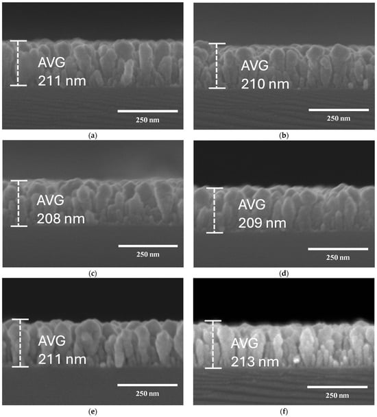
Figure 5.
Cross-section images of FE-SEM analysis on ITO-nanorod deposited on glass substrate treated with oxygen plasma of varying gas flow rates compared with ASD film: (a) ASD; (b) 20 sccm; (c) 40 sccm; (d) 60 sccm; (e) 80 sccm; (f) 100 sccm.
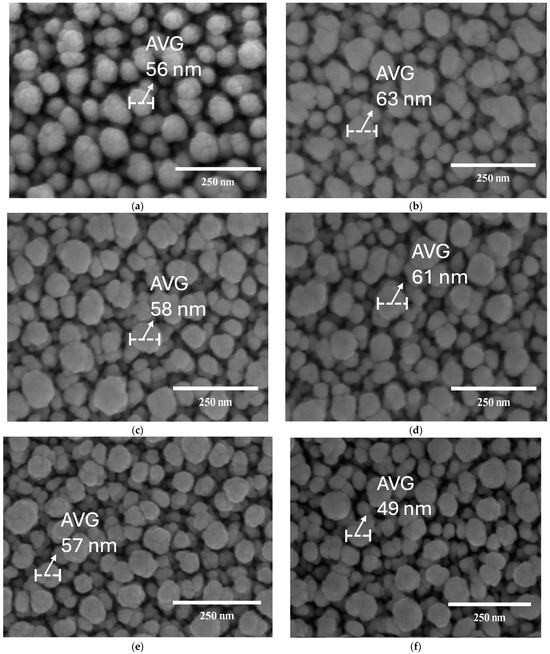
Figure 6.
Top-image of FE-SEM analysis (top view) of an ITO-nanorod deposited on glass substrate treated with oxygen plasma of varying gas flow rates compared with as-deposited film: (a) ASD; (b) 20 sccm; (c) 40 sccm; (d) 60 sccm; (e) 80 sccm; (f) 100 sccm.
To further investigate the topography of the ITO-nanorod surface treated with oxygen plasma, Figure 7 illustrates the AFM images. The AFM images in Figure 7 show the formation of nanorod structures in the different variations of film roughness with sizes of 1.00 m × 1.00 m. As can be seen, there has been a deep hole and roughness on the surface of ITO films. To explore in more detail, a convex area is formed by the deposition of a high-density ITO-nanorod film prepared by E-beam evaporation with the glancing angle deposition method, and the dark color is formed by the treatment of the film surface with oxygen plasma, thus forming a concave area on the film surface. According to Figure 6, the size of the nanorod decreases with the increasing oxygen flow rate, especially at 100 sccm with the size of 49 nm. Moreover, to confirm the exact results from the oxygen plasma treatment of the ITO-nanorod surface, the highest value of roughness analysis of about 9 nm at an oxygen gas flow rate of 100 sccm is presented in Figure 8. In this case, it can be explained that with the oxygen plasma treatment at a higher oxygen gas flow rate, the collision between the plasma ions and the ITO ions on the surface is caused by the ions strike of high-energy gas ions via the sputtering method, which leads to increased kinetic energy and more surface treatment, thus achieving higher surface roughness.
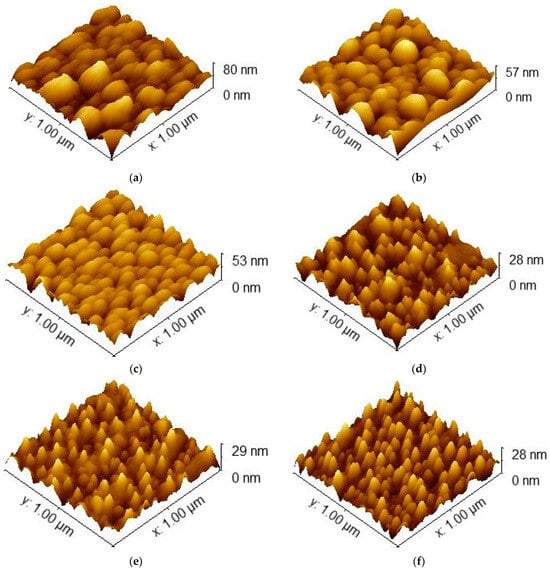
Figure 7.
AFM images determining the structural roughness of ITO-nanorod deposited on glass substrate treated with oxygen plasma under different conditions of oxygen gas supply: (a) ASD; (b) 20 sccm; (c) 40 sccm; (d) 60 sccm; (e) 80 sccm; (f) 100 sccm.
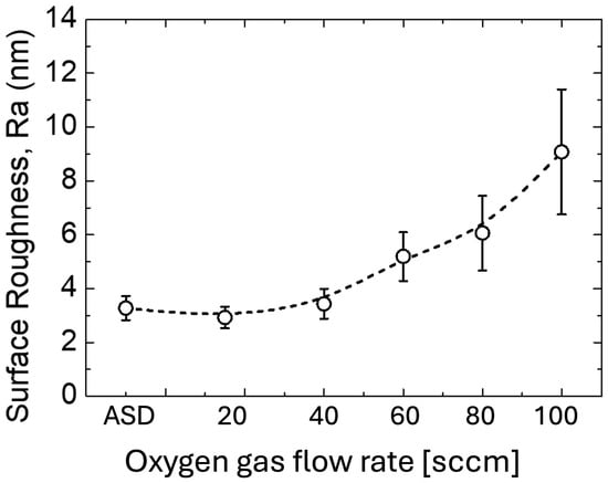
Figure 8.
Surface roughness parameters of oxygen plasma treatment on ITO-nanorod films from 1.00 m 1.00 m AFM scan samples with different conditions of oxygen gas flow rates, including ASD, 20, 40, 60, 80, and 100 sccm.
Additionally, the diameter and length of ITO-nanorod structures treated with oxygen plasma at different flow rates were analyzed, and the average values were calculated using Gaussian distribution [41] according to Equation (5).
where the Gaussian function value is , a is the mean value, the standard deviation is , and X is the diameter measurement of each grain in nanometers. Figure 9 illustrates the relationship graph from the calculation of the diameter and length of ITO-nanorod, which compares the samples between ASD film and ITO-nanorod treated with oxygen plasma. Looking in more detail at Figure 9, the graph shows that at flow rates of 20–80 sccm, the nanorod sizes are quite similar, and when the flow rate is increased to 100 sccm, the oxygen plasma concentration is the highest, which causes the highest plasma energy to break the bonds of the ITO surface. For this, the nanorod size is the smallest compared to other conditions. The results exhibit that the adjustment of oxygen gas flow rate in the plasma process affects the change in the size of the nanorods, with the length of ITO-nanorods ranging from 208 to 213 nm. When considering the size of the nanorods in the blue graph at different oxygen gas flow rates, it was found that when the oxygen gas flow rate increased, the nanorod size gradually decreased. This can be explained by the fact that as the oxygen plasma ion concentration increases, the neutral gas molecules or atoms and the excited gas molecules and atoms will have a large amount of internal energy. When these molecules, ions, and atoms come together, they interact with the ITO-nanorod surface, resulting in well-separated nanorod structures because of the shadowing effect [42]. This causes the gas atoms to fall onto the support and not aggregate into a film layer, resulting in separated and smaller ITO-nanorod structures [43,44]. Similarly, the nanorods show the smallest size at a flow rate of 100 sccm compared with other flow rate conditions. At a flow rate of 100 sccm, the concentration of oxygen particles is the highest when the plasma is generated, resulting in the ionization of a large amount of oxygen gas. In this case, when stimulated by a biased process, causing more energy to break the bonds on ITO-nanorod surfaces, resulting in smaller nanorod size, the bond-breaking reaction can be seen in Figure 3.
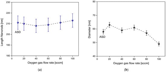
Figure 9.
Relationship of length nanorods and diameter size on ITO-nanorod calculated by Gaussian distribution compared between ASD film and oxygen plasma treatment at 20, 40, 60, 80, and 100 sccm: (a) length nanorods; (b) diameter nanorods.
3.2. Optical Properties
The light transmittance was analyzed by a spectrophotometer measuring from the 250 to 2000 nm wavelength range. The comparison between glass substrate, ASD film, and ITO-nanorod treated with oxygen plasma of varying gas content at 20, 40, 60, 80, and 100 sccm is displayed in Figure 10. From the spectral lines, it was found that the light transmittance of the plasma-treated ITO-nanorod film was in a good range and was close to each other in the visible wavelength range of 380–750 nm, which is the appropriate wavelength. The overall transmittance values are approximately 85%.
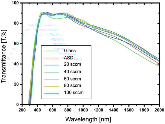
Figure 10.
Transmittance spectra of the ITO-nanorod films compared with clear glass, as-deposited film, and treated with oxygen plasma content of 20, 40, 60, 80, and 100 sccm prepared via bias-magnetron RF sputtering process.
Furthermore, the average transmittance in the visible range (400–700 nm) of ITO-nanorod films treated with oxygen plasma under different gas flow rates of 20, 40, 60, 80, and 100 sccm was calculated and compared with glass, ASD film, and ITO commercial, as shown in Figure 11. As can be seen in the graph, the average transmittance in the visible range of the plasma-treated ITO-nanorod film increases with the increase in the oxygen gas flow rate. Due to the increased self-collision of oxygen ions at higher concentrations, a correspondingly higher average transmittance change is achieved. Then, the omnidirectional characteristics were analyzed at 500, 600, and 700 nm wavelengths of the glass substrate, as-deposited film, and treated with oxygen plasma of varying gas 20, 40, 60, 80, and 100 sccm. It was measured at the incident angle between 0 and 80. The analysis results are illustrated in Figure 12, Figure 13 and Figure 14. From the spectrum, the results found that a percentage of light-transmittance at incident angles of ITO-nanorod treated with oxygen plasma was close in overall cases of gas content. Compared with glass, ITO-nanorod films treated with oxygen plasma have a higher light transmittance. Therefore, optimizing light transmittance value is suitable as a thin transparent conductive oxide film in solar cells.
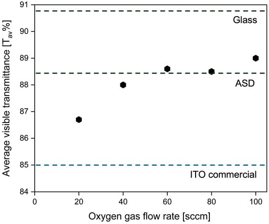
Figure 11.
Average transmittance in the visible range of the ITO-nanorod films compared with clear glass, ASD film, and treated with oxygen plasma content of 20, 40, 60, 80, and 100 sccm prepared via bias-magnetron RF sputtering process.
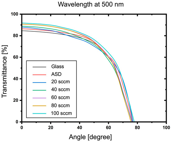
Figure 12.
Omnidirectional characteristics on transmittance properties of ITO-nanorod treated with oxygen plasma under gas content 20, 40, 60, 80, and 100 sccm compared to glass substrate and ASD film at 500 nm-wavelength.
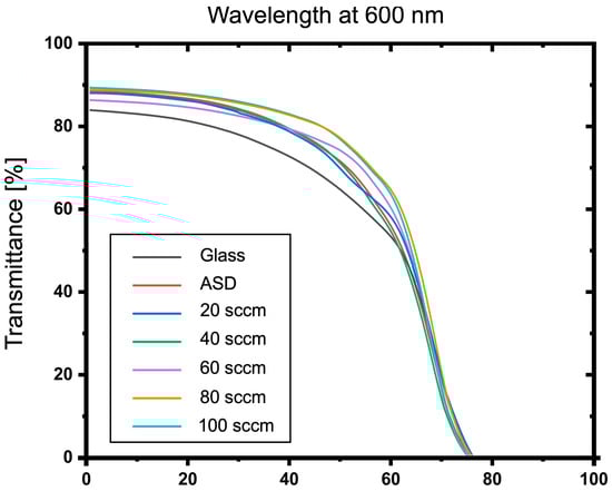
Figure 13.
Omnidirectional characteristics on transmittance properties of ITO-nanorod treated with oxygen plasma under gas content 20, 40, 60, 80, and 100 sccm compared to glass substrate and ASD film at 600 nm-wavelength.
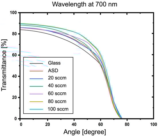
Figure 14.
Omnidirectional characteristics on transmittance properties of ITO-nanorod treated with oxygen plasma under gas content 20, 40, 60, 80, and 100 sccm compared to glass substrate and ASD film at 700 nm-wavelength.
3.3. Electrical Properties
Figure 15 shows the electrical properties of ITO-nanorod treated with oxygen plasma at gas contents 20, 40, 60, 80, and 100 sccm, compared to ASD film. From the electrical properties test results, it was found that when the oxygen gas flow rate increased, the sheet resistance value gradually decreased. It was found that the oxygen gas flow rate of 100 sccm showed the lowest sheet resistance value. On the contrary, the ASD film gave the highest sheet resistance value. In this, the decrease in sheet resistance is because of the bombardment of oxygen ions with the film surface with the highest oxygen concentration. Thus, it has a higher ability to attack the ITO-nanorod film surface, which exhibits the lowest sheet resistance. With this low resistance, ITO-nanorod films will greatly benefit DSSCs, as they will enable efficient charge transfer and reduce energy loss in the cells.
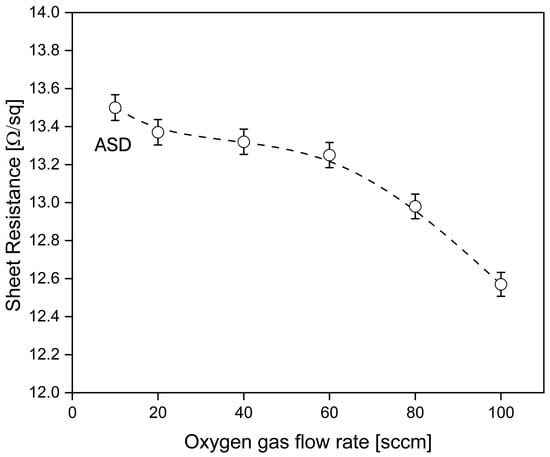
Figure 15.
Electrical properties on ITO-nanorod film treated with oxygen plasma compared with ASD film using four-point probe technique.
3.4. Efficiency of DSSCs
The photovoltaic (PV) performance of the fabricated DSSC devices with the ITO film is evaluated. Figure 16a shows an image of the fabricated ITO-nanorod-based DSSC sample experimentally used in this work. As can be seen in Figure 16b, the ITO-nanorod film is an electron-collecting layer. TiO2 nanoparticles of 15–20 nm size are interconnected in three dimensions on the ITO-nanorod layer. For this, many dye molecules injected into the TiO2 nanoparticle layer will adhere to the large surface of nanoparticles, enabling efficient harvesting. In this work, the TiO2 paste was provided by the sol-gel combustion method with a thickness of 10 μm, which was coated on glass by the screen-printing technique.
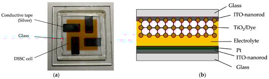
Figure 16.
Images of the ITO-nanorod based on DSSC device created with DSSC cell size 2.5 cm × 2.5 cm: (a) assemble cells of DSSC device; (b) model of cell structural.
In this part, the short-circuit current was received without external potential. The efficiency of DSSC devices was calculated concerning the solar spectrum by calibrating a 1000-light drive lamp with direct sunlight. The efficiency of photon-to-current conversion was indicated by the range of 450–700 nm when measuring the light intensity. The photocurrent (I) and photovoltage (V) of the ITO-nanorod-based DSSC devices were carefully measured. In the measurement, an ITO-nanorod film with an active area of 0.2 cm2 was annealed at 250°C through simulated sunlight at AM-1.5 generated by a 200 W solar simulator. Jsc is the total photocurrent density or the current obtained under short-circuit conditions divided by the cell area. The Voc is the open circuit voltage, and FF is the fill factor related to the series resistance for practical solar cells. In addition, electrical impedance measurements were performed via Voc under no-current conditions.
In the PV performance, the DSSCs structure is defined as follows: ITO-nanorod treated with oxygen plasma used as a working electrode, deposited with TiO2, N 719 dye used as the photosensitizer, used as an electrolyte [45], and platinum (Pt) used as the counter electrode. Thus, the assembly structure of the DSSC device is glass-deposited ITO-nanorod/TiO2/()/Pt, respectively [46,47,48,49]. Figure 17 illustrates the I–V characterization on ITO-nanorod film applied with DSSC devices. The overall η of DSSCs, meaning the percentage of solar energy that shines on a photovoltaic device, which is converted into electricity, was tested by Jsc, Voc, and FF, which are calculated by Equation (5) [50], as shown in Table 1.
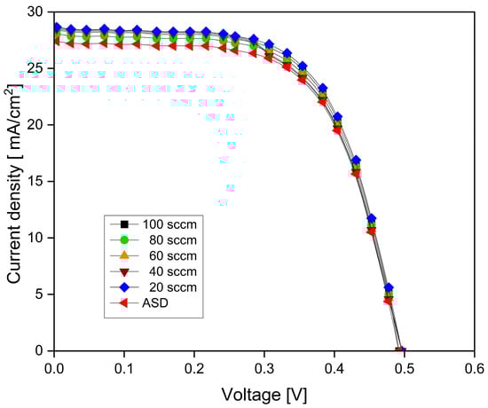
Figure 17.
I–V characteristics of DSSCs on ITO-nanorod treated with oxygen plasma of varying gas contents at 20, 40, 60, 80, and 100 sccm provided via bias-magnetron RF sputtering process.

Table 1.
Photovoltaic parameters of DSSCs based on the ITO-nanorod films treated with oxygen plasma of varying gas contents at 20–100 sccm.
Figure 18 shows the overall efficiency of DSSC devices, comparing ASD film and ITO-nanorod film treated with oxygen plasma in different conditions of gas flow rates. The trend illustrates that when the oxygen gas flow rate is increased, the η of the photovoltaic improves. Compared with ASD film, the samples treated with oxygen plasma exhibited higher efficiency, especially at an oxygen gas flow rate of 100 sccm, showing the highest efficiency of 9.5%. It produces higher energy oxygen plasma with more oxygen gas ions. When falling to ITO-nanorod substrates, the substrate surface is modified by enhancing the roughness of the ITO-nanorod (working electrode) to allow greater dye absorption. This results in better light harvesting efficiency, leading to improved performance of DSSC devices based on ITO-nanorod deposited on a glass substrate.
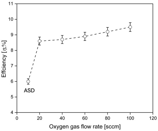
Figure 18.
Variability of data on graphs to indicate the error in the efficiency of DSSCs on ITO-nanorod treated with oxygen plasma of varying gas contents at 20, 40, 60, 80, and 100 sccm provided via bias-magnetron RF sputtering process.
The result can be explained by the relatively low electrical resistance in Figure 15 of the ITO film, which significantly affects the measured current. When electrons are injected from the dye molecules into the TiO2 nanoparticles with light energy, then the electrons are mobilized through the network of the TiO2 and ITO-nanorod layers. Nonetheless, the electrical entanglement of the TiO2/ITO-nanorod layers is not good enough to move across the interface during diffusion. In that case, the current density will decrease, resulting in a lower measured current density. Thus, solar cell efficiency can be improved by treating ITO with oxygen plasma. Since the ITO-nanorod was treated with oxygen plasma, the film structure changed, such that when the gas flow rate was increased, the size of the nanorods became smaller and separated because of the plasma treatment. Therefore, it affects the efficiency of converting solar energy into electrical energy for DSSC devices. In this, the obtained result can be explained that when the ITO film surface becomes rougher, sunlight (photon) will pass the device through the working electrode layer and react with the TiO2/dye layer, resulting in a large number of electrons that attach to the ITO film layer at the top layer. Thus, there is a high amount of electric current and Voc, resulting in electrons having much energy to transport to the counter electrode, which improved the ITO films’ semiconductor properties as shown in Figure 19.
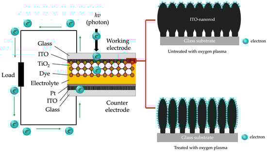
Figure 19.
Schematic structure and principle of operation of DSSC devices based on ITO-nanorod prepared with oxygen plasma treatment via bias-magnetron RF sputtering process.
4. Discussion
The study’s main objective is to create a new material for working electrodes to achieve DSSC with cost-effective, environmentally sustainable, and simple synthesis. This research emphasizes the critical use of plasma technology to modify the material’s surface to investigate a relationship between the structure of the dye and the device’s performance. This is necessary to know to develop new devices using environmentally friendly materials. Regarding the proposed stability, the critical issue is to improve the efficiency of solar energy conversion to meet the demand for electricity and energy. Therefore, we propose to improve the efficiency of DSSCs based on the use of plasma technology to attack the material surface at the nanoscale level of the working electrode layer. It can be confirmed that plasma technology can penetrate the nanoscale particles to break the bonds and produce suitable properties for application.
The research results found that using plasma to treat the material surface with different gas flow rates affected several properties of the film. At first, in terms of the structure of the film layer, the result shows that when the oxygen gas flow rate is increased, the nanostructure of the ITO layer changes, and the grain size decreases because of the plasma attack on the In3+/Sn4+ bonds. Secondly, when the oxygen gas flow rate is increased, the result exhibits improved optical properties of the film, which is suitable for use as transparent conductive properties in solar cell devices. Thirdly, when the oxygen gas flow rate increases, the sheet resistance decreases, which is an advantage of the electrical properties that will help the solar cell device transfer charge quickly and reduce energy loss. Finally, when the oxygen gas flow rate increases, the η can be increased compared to the average film not treated with plasma.
Therefore, in the near future, we will develop a simple treatment system using low-cost materials such as nitrogen gas or atmospheric pressure to prepare ITO films with better quality and solar cell performance with oxygen plasma treatment.
5. Conclusions
This work successfully fabricated ITO-nanorod films using E-beam evaporation with the glancing angle deposition method. Nanorods illustrated the obtained films. The ITO-nanorod film was treated with oxygen plasma via a bias-magnetron RF sputtering process. To investigate the exceptional result, the oxygen gas flow rate varied by 20, 40, 60, 80, and 100 sccm. Thus, the oxygen plasma treatment has been proven effective in promoting the crystallization of ITO films, resulting in changes in their optical and electrical properties. Notably, the efficiency of DSSC devices can improve through oxygen plasma treatment.
Author Contributions
Conceptualization, W.P. and N.M.; methodology, S.A.; software, T.T.; validation, W.P. and N.K.; formal analysis, S.A. and T.T.; investigation, A.S. (Apidat Songruk); resources, N.K.; data curation, W.P.; writing—original draft preparation, N.M. and A.S. (Anumut Siricharoenpanich); writing—review and editing, S.A.; visualization, T.M. and K.T.; supervision, N.K.; project administration, N.M. All authors have read and agreed to the published version of the manuscript.
Funding
This research was funded by the Royal Golden Jubilee (RGJ) Ph.D scholarship from the National Research Council of Thailand under the Ministry of Higher Education, Science, Research, and Innovation, grant number N41A650091. This work is also supported by the project of the Research, Innovation, Partnerships Office (RIPO), with Financial Support from the Faculty of Industrial Education and Technology.
Data Availability Statement
The original contributions presented in the study are included in the article, further inquiries can be directed to the corresponding authors.
Acknowledgments
The materials and equipment are supported by Faculty of Engineering, Kyungsung University and Faculty of Education, University of Miyazaki, Japan.
Conflicts of Interest
The authors declare no conflicts of interest.
References
- Tedla, A.; Tai, Y. Influence of binary solvent system on the stability and efficiency of liquid dye sensitized solar cells. J. Photochem. Photobiol. A Chem. 2018, 358, 70–75. [Google Scholar] [CrossRef]
- Han, K.-S.; Shin, J.-H.; Yoon, W.-Y.; Lee, H. Enhanced performance of solar cells with anti-reflection layer fabricated by nano-imprint lithography. Sol. Energy Mater. Sol. Cells 2011, 95, 288–291. [Google Scholar] [CrossRef]
- Agrawal, N.; Ansari, M.Z.; Majumdar, A.; Gahlot, R.; Khare, N. Efficient up-scaling of organic solar cells. Sol. Energy Mater. Sol. Cells 2016, 157, 960–965. [Google Scholar] [CrossRef]
- Sharma, K.; Sharma, V.; Sharma, S.S. Dye-sensitized solar cells: Fundamentals and current status. Nanoscale Res. Lett. 2018, 13, 381. [Google Scholar] [CrossRef] [PubMed]
- Bu, I.Y.Y.; Zheng, J. A new type of counter electrode for dye sensitized solar cells based on solution processed SnO2 and activated carbon. Mater. Sci. Semicond. 2015, 39, 223–228. [Google Scholar] [CrossRef]
- Kao, M.C.; Chen, H.Z.; Young, S.L. Dye-sensitized solar cells with TiO2 nanocrystalline films prepared by conventional and rapid thermal annealing processes. Thin Solid Film. 2011, 519, 3268–3271. [Google Scholar] [CrossRef]
- Kumar, A.; Goyal, A.K.; Gupta, U.; Tanya Gupta, N.; Chaujar, R. Increased efficiency of 23% for CIGS solar cell by using ITO as front contact. Mater. Today Proc. 2020, 28, 361–365. [Google Scholar] [CrossRef]
- Bett, A.J.; Winkler, K.M.; Bivour, M.; Cojocaru, L.; Kabakli, O.S.; Schulze, P.S.C.; Siefer, G.; Tutsch, L.; Hermle, M.; Glunz, S.W.; et al. Semi-transparent perovskite solar cells with ITO directly sputtered on spiro-OMeTAD for tandem applications. ACS Appl. Mater Interfaces 2019, 11, 45796–45804. [Google Scholar] [CrossRef]
- Chavan, G.T.; Kim, Y.; Khokhar, M.Q.; Hussian, S.Q.; Cho, E.-C.; Yi, J.; Ahmad, Z.; Rosaiah, P.; Jeon, C.-W. A brief review of transparent conducting oxides (TCO): The influence of different deposition techniques on the efficiency of solar cells. Nanomaterials 2023, 13, 1226. [Google Scholar] [CrossRef]
- Peng, Y.; Zhang, L.; Cheng, N.; Andrew, T.L. ITO-free transparent organic solar cell distributed bragg reflector for solar harvesting windows. Energies 2017, 10, 707. [Google Scholar] [CrossRef]
- Shikoh, A.S.; Ahmad, Z.; Touati, F.; Shakoor, R.A.; Al-Muhtaseb, S.A. Optimization of ITO glass/TiO2 based DSSC photo-anodes through electrophoretic deposition and sintering techniques. Ceram. Int. 2017, 43, 10540–10545. [Google Scholar] [CrossRef]
- Upadhyaya, H.M.; Senthilarasu, S.; Hsu, M.-H.; Kumar, D.K. Recent progress and the status of dye-sensitised solar cell (DSSC) technology with state-of-the-art conversion efficiencies. Sol. Energy Mater. Sol. Cells 2013, 119, 291–295. [Google Scholar] [CrossRef]
- Wang, Z.; Fang, J.; Mi, Y.; Zhu, X.; Ren, H.; Liu, X.; Yan, Y. Enhanced performance of perovskite solar cells by ultraviolet-ozone treatment of mesoporous TiO2. Appl. Surf. Sci. 2018, 436, 596–602. [Google Scholar] [CrossRef]
- Cho, J.M.; Kwak, S.-W.; Aqoma, H.; Kim, J.W.; Shin, W.S.; Moon, S.-J.; Jang, S.-Y.; Jo, J. Effects of ultraviolet-ozone treatment on organic-stabilized ZnO nanoparticle-based electron transporting layers in inverted polymer solar cells. Org. Electron. 2014, 15, 1942–1950. [Google Scholar] [CrossRef]
- Farina, F.E.; Azmi, W.S.B.; Harafuji, K. Ultraviolet-ozone anode surface treatment and its effect on organic solar cells. Thin Solid Film. 2017, 623, 72–83. [Google Scholar] [CrossRef]
- Ahmed, N.M.; Sabah, F.A.; Abdulgafour, H.I.; Alsadig, A.; Sulieman, A.; Alkhoaryef, M. The effect of post annealing temperature on grain size of indium-tin-oxide for optical and electrical properties improvement. Results Phys. 2019, 13, 102159. [Google Scholar] [CrossRef]
- Legnani, C.; Lima, S.A.M.; Oliveria, H.H.S.; Quirino, W.G.; Machado, R.; Santos, R.M.B.; Davolos, M.R.; Achete, C.A.; Cremona, M. Indium tin oxide films prepared via wet chemical route. Thin Solid Film. 2007, 516, 193–197. [Google Scholar] [CrossRef]
- Khachatryan, H.; Kim, D.-J.; Kim, M.; Kim, H.-K. Roll-to-Roll fabrication of ITO thin film for flexible optoelectronics applications: The role of post-annealing. Mater. Sci. Semicond. 2018, 88, 51–56. [Google Scholar] [CrossRef]
- Qin, G.; Fan, L.; Watanabe, A. Formation of indium tin oxide film by wet process using laser sintering. J. Mater. Process. Technol. 2016, 227, 16–23. [Google Scholar] [CrossRef]
- Khadtare, S.; Bansode, A.S.; Mathe, V.L.; Shrestha, N.K.; Bathula, C.; Han, S.-H.; Pathan, H.M. Effect of oxygen plasma treatment on performance of ZnO based dye sensitized solar cells. J. Alloys Compd. 2017, 784, 348–352. [Google Scholar] [CrossRef]
- He, P.; Wang, S.D.; Wong, W.K.; Cheng, L.F.; Lee, C.S.; Lee, S.T.; Liu, S.Y. Vibrational analysis of oxygen-plasma treated indium tin oxide. Chem. Phys. Lett. 2003, 370, 795–798. [Google Scholar] [CrossRef]
- Lu, D.; Wu, Y.; Guo, J.; Lu, G.; Wang, Y.; Shen, J. Surface treatment of indium tin oxide by oxygen-plasma for organic light-emitting diodes. Mater. Sci. Eng. B. 2003, 97, 141–144. [Google Scholar] [CrossRef]
- Park, Y.S.; Kim, E.; Hong, B.; Lee, J. Characteristics of ITO films with oxygen plasma treatment for thin film solar cell applications. Mater. Res. Bull. 2013, 48, 5115–5120. [Google Scholar] [CrossRef]
- He, K.; Yang, X.; Yan, H.; Wu, Z.; Li, Z.; Zhong, S.; Ou, Q.; Liang, R. Work function changes of plasma treated indium tin oxide. Org. Electron. 2014, 15, 1731–1737. [Google Scholar] [CrossRef]
- Yahya, M.; Fadavieslam, M.R. Effect of oxygen plasma on ITO surface and OLED physical properties. Microelectron. Reliab. 2023, 144, 114981. [Google Scholar] [CrossRef]
- Gao, X.; Lin, B.; Lin, J.; Chen, H.; Wu, Z. Improving the performance of organic light-emitting devices by employing oxygen plasma treatment on indium-tin-oxide surfaces. Displays 2023, 76, 102373. [Google Scholar] [CrossRef]
- Calnan, S.; Upadhyaya, H.M.; Dann, S.E.; Thwaites, M.J.; Tiwari, A.N. Effects of target bias voltage on indium tin oxide films deposited high target utilisation sputtering. Thin Solid Film. 2007, 515, 8500–8504. [Google Scholar] [CrossRef]
- Maissel, L.I.; Schaible, P.M. Thin films deposited by bias sputtering. J. Appl. Phys. 1965, 36, 237–242. [Google Scholar] [CrossRef]
- Stamate, E. Lowering the resistivity of aluminum doped zinc oxide thin films by controlling the self-bias during RF magnetron sputtering. Surf. Coat. Technol. 2020, 402, 126306. [Google Scholar] [CrossRef]
- Liang, L.Y.; Cao, H.T.; Liu, Q.; Jiang, K.M.; Liu, Z.M.; Zhuge, F.; Deng, F.L. Substrate biasing effect on the physical properties of reactive RF-magnetron-sputtered aluminum oxide dielectric films on ITO glasses. ACS Appl. Mater. Interfaces 2014, 6, 2255–2261. [Google Scholar] [CrossRef]
- Lee, J.; Jung, H.; Lim, D.; Yang, K.; Song, W.; Yi, J. Effects of bias voltage on the properties of ITO films prepared on polymer substrates. Thin Solid Film. 2005, 480–481, 157–161. [Google Scholar] [CrossRef]
- Zhao, L.; Zhou, Z.; Peng, H.; Cui, R. Indium tin oxide thin films by bias magnetron rf sputtering for heterojunction solar cells application. Appl. Surf. Sci. 2005, 252, 385–392. [Google Scholar] [CrossRef]
- Honda, S.-I.; Chihara, K.; Watamori, M.; Oura, K. Depth profiling of oxygen content of indium tin oxide fabricated by bias sputtering. Appl. Surf. Sci. 1997, 113–114, 408–411. [Google Scholar] [CrossRef]
- Perez, I.; Sosa, V.; Perera, F.G.; Galindo, J.T.E.; Enriquez-Carrejo, J.L.; Gonzalez, P.G.M. Effect of ion bombardment on the chemical properties of crystalline tantalum pentoxide films. Vacuum 2019, 165, 274–282. [Google Scholar] [CrossRef]
- Rizzo, A.; Signore, M.A.; Valerini, D.; Altamura, D.; Cappello, A.; Tapfer, L. A study of suppression effect of oxygen contamination by bias voltage in reactively sputtered ZrN films. Surf. Coat. Technol. 2012, 206, 2711–2718. [Google Scholar] [CrossRef]
- Yamamoto, T.; Nomoto, J.; Kitami, H.; Sakemi, T.; Makino, H.; Kobayashi, K.; Aoki, Y.; Kishimoto, S. Design of advanced functional ZnO conductive thin films with arc plasma. J. Vac. Soc. Jpn. 2017, 60, 292–299. [Google Scholar] [CrossRef]
- Holland, L.; Ojha, S.M. The chemical sputtering of graphite in an oxygen plasma. Vacuum 1976, 26, 53–60. [Google Scholar] [CrossRef]
- Rosemann, N.; Ortner, K.; Petersen, J.; Schadow, T.; Baker, M.; Brauer, G.; Rosler, J. Influence of bias voltage and oxygen flow rate on morphology and crystallographic properties of gas flow sputtered zirconia coatings. Surf. Coat. Technol. 2015, 276, 668–676. [Google Scholar] [CrossRef]
- Brewer, S.H.; Franzen, S. Calculation of the electronic and optical properties of indium tin oxide by density functional theory. Chem. Phys. 2004, 300, 285–293. [Google Scholar] [CrossRef]
- Ma, H.L.; Zhang, D.H.; Ma, P.; Win, S.Z.; Li, S.Y. Preparation and properties of transparent conducting indium tin oxide films deposited by reactive evaporation. Thin Solid Films 1995, 263, 105–110. [Google Scholar] [CrossRef]
- Gaussian Function. Available online: https://en.wikipedia.org/wiki/Gaussian_function (accessed on 15 February 2024).
- Galagan, Y.; Zimmermann Coenen, E.W.C.; Jorgensen, M.; Tanenbaum, D.M.; Krebs, F.C.; Gorter, H.; Sabik, S.; Slooff, L.H.; Veenstra, S.C.; Kroon, J.M.; et al. Current collecting grids for ITO-Free solar cells. Adv. Energy Mater. 2012, 2, 103–110. [Google Scholar] [CrossRef]
- Cardinaud, C.; Peignon, M.-C.; Tessier, P.-Y. Plasma etching: Principles, mechanisms, application to micro- and nano-technologies. Appl. Surf. Sci. 2000, 164, 72–83. [Google Scholar] [CrossRef]
- Coburn, J.W.; Winters, H.F. Ion- and electron-assisted gas-surface chemistry—An important effect in plasma etching. J. Appl. Phys. 1979, 50, 3189–3196. [Google Scholar] [CrossRef]
- Tennakone, K.; Kumara, G.R.R.A.; Kottegoda, I.R.M.; Perera, V.P.S. An efficient dye-sensitized photoelectrochemical solar cell made from oxides of tin and zinc. Chem. Comn. 1999, 1, 15–16. [Google Scholar] [CrossRef]
- Fung, A.K.M.; Chiu, B.K.W.; Lam, M.H.W. Surface modification of TiO2 by a ruthenium (II) polypyridyl complex via silyl-linkage for sensitized photocatalytic degradation of carbon tetrachloride by visible irradiation. Water Res. 2003, 37, 1939–1947. [Google Scholar] [CrossRef]
- Zaban, A.; Ferrere, S.; Gregg, B.A. Relative Energetics at the semiconductor/sensitizing dye/electrolyte interface. J. Phys. Chem. B 1998, 102, 452–460. [Google Scholar] [CrossRef]
- Fakharuddin, A.; Jose, R.; Brown, T.M.; Fabregat-Santiago, F.; Bisquert, J. A perspective on the production of dye-sensitized solar modules. Energy Environ. Sci. 2014, 7, 3952–3981. [Google Scholar] [CrossRef]
- Wang, M.; Anghel, A.M.; Marsan, B.; Cevey Ha, N.L.; Pootrakulchote, N.; Zekeeruddin, S.M.; Grätzel, M. CoS supersedes Pt as efficient electrocatalyst for triiodide reduction in dye-sensitized solar cells. J. Am. Chem. Soc. 2009, 131, 15976–15977. [Google Scholar] [CrossRef]
- Murakami, T.N.; Gratzel, M. Counter electrode for DSC: Application of functional materials as catalysts. Inorganica Chim. Acta 2008, 361, 572–580. [Google Scholar] [CrossRef]
Disclaimer/Publisher’s Note: The statements, opinions and data contained in all publications are solely those of the individual author(s) and contributor(s) and not of MDPI and/or the editor(s). MDPI and/or the editor(s) disclaim responsibility for any injury to people or property resulting from any ideas, methods, instructions or products referred to in the content. |
© 2024 by the authors. Licensee MDPI, Basel, Switzerland. This article is an open access article distributed under the terms and conditions of the Creative Commons Attribution (CC BY) license (https://creativecommons.org/licenses/by/4.0/).