1. Introduction
In recent years, dye-sensitized solar cells (DSSCs) have become an attractive renewable energy technology due to their low manufacturing cost, simple process, and low requirements on light sources. In addition, DSSCs have good photoelectric conversion efficiency under low-light conditions, which makes them advantageous indoors and in dark environments. These advantages enable DSSCs to show great potential in building-integrated applications and emerging markets [
1,
2]. Dye-sensitized solar cells (DSSCs) are composed of dyes, nanoporous metal oxide photoanode materials, electrolytes, and counter electrodes. Nanoporous metal oxides play a key role in improving the photoelectric conversion efficiency of DSSCs. In recent years, a lot of wide-band metal oxides have been employed as photoanodes in that TiO
2 gained more attention due to its charge transport capability, large surface area nanostructure, high diffusion rate, and chemical stability for the development of high-performance DSSCs [
3,
4]. However, TiO
2 exhibits low efficiency owing to its high electron-recombination rate and low dye-adsorption rate [
5,
6,
7,
8]. Research has been carried out on the improvement of the optical and electrical properties of TiO
2 photoanodes by doping with transition metal ions such as Cu, Zn, Zr, and W [
9,
10,
11,
12]. The incorporation of reduced graphene oxide has also been reported to enhance the charge collection and reduce electron recombination rates, further boosting DSSC performance. These modifications represent important advancements in the design of high-performance DSSCs. Doping TiO
2 with W increases the specific surface area, dye adsorption capacity, and the generation of electrons and free radicals, enhancing the flow of charge in DSSCs [
13,
14,
15,
16]. Various synthesis methods have been explored for W-doped TiO
2. For example, Archana et al. synthesized W-doped TiO
2 nanowires through electrospinning, resulting in an increase in solar cell efficiency from 4.14% to 8.17% [
13]. Cant et al. achieved 8.9% efficiency using tungsten-doped mesoporous titanium dioxide spheres as DSSC photoanodes [
14]. Momeni synthesized W-doped TiO
2 nanotubes via electrochemical anodizing, achieving 2.34% efficiency [
15]. Bhabu used a solid-phase method to prepare a 20 mol% tungsten-doped TiO
2 photoanode, improving DSSC efficiency from 1.03% to 2.47% [
16].
In contrast to these methods, our study employs the sol–gel technique, which presents unique advantages that make it an ideal choice for fabricating W-doped TiO2 thin films. The sol–gel method enables the use of cost-effective precursors and a straightforward synthesis process, ensuring a uniform W distribution and precise stoichiometric control. This precise control allows for the fine-tuning of film properties, such as thickness, porosity, and crystallinity, to optimize light absorption, electron transport, and dye-loading capacity—critical factors in enhancing DSSC performance. Furthermore, our research demonstrates that using a 6 at% W-doping concentration optimizes these properties, achieving a higher efficiency compared to previously reported methods.
In this paper, the TiO2 thin films doped with tungsten at different proportions for DSSCs were fabricated using sol–gel technology and deposited on FTO-coated glass substrates. The effects of the amount of W6+ dopant on the microstructure, optical, and photovoltaic properties were studied. The structural, optical, morphological, and optoelectronic properties of W-doped TiO2 thin films were studied using XRD, SEM, XPS, and BET analysis. DSSCs were prepared using W-doped TiO2 thin films. The effect of W doping on the photoelectric performance of DSSCs was studied by analyzing the I–V curve and incident monochromatic photo-to-current conversion efficiency (IPCE) under AM 1.5G solar radiation.
2. Materials and Methods
In the sol–gel process, titanium diisoprop-oxide bis (2,4-pentanedionate) (TIAA), Ti(OC3H7)2 (CH3COCHCOCH3)2 (Alfa, 99.9%+ purity), tungsten isopropoxide, and W[OCH(CH3)2]6 (Alfa, 99.9%+ purity) were used as precursor, and 2-methoxyethanol and C3H8O2 (Fluka, 99.9%+ purity) were used as solvents. First, diisoprop-oxide bis (2,4-pentanedionate) and 2-methoxyethanol were stirred at room temperature for 1 h in an ambient atmosphere, then tungsten isopropoxide was added into the solution and was refluxed at 120 °C in an ambient atmosphere for 4 h. During the production process, it was necessary to ensure that the precursor was evenly dispersed in the solvent. The evaporation rate of the solvent must be controlled to form a gel structure during the reflux process. The molar concentrations of W relative to TiO2 in the tungsten-doped TiO2 precursor solution were 0, 2, 4, 6, and 8 at%, respectively. The solution was then cooled to 80 °C for 2 h under an ambient atmosphere to promote homogeneity. Finally, the solution was cooled to room temperature to complete the production. The formed tungsten-doped TiO2 gel was further subjected to rapid high-temperature annealing to remove residual solvents and organic matter to form the desired structure.
The W-doped TiO2 solution was spin-coated on the FTO-coated glass substrate using a commercial photoresist spinner, and the spin rate was divided into two steps: 1000 rpm and 3000 rpm for 10 s and 30 s, respectively. After each coating step, the W-doped TiO2 gel films were annealed on a hot plate at 300 °C for 2 min. A total of 10 coating steps were completed before final rapid thermal annealing. After the last coating step was completed, the W-doped TiO2 gel film was annealed with rapid thermal annealing at 600 °C for 2 min in an oxygen atmosphere with an annealing rate of 600 °C/min. After rapid thermal annealing, the thickness of the W-doped TiO2 thin film after multilayer coating was 2 μm, measured using an α-order surface profilometer. The average thickness of the single-coat sintered layer for all samples was approximately 0.2 μm. Undoped titanium dioxide is named TiO2, while all W-doped TiO2 films are named TiO2-W2, TiO2-W4, TiO2-W6, and TiO2-W8 according to their dopant molar concentrations, 2, 4, 6, and 8 at%, respectively.
The crystal structure and microstructure of W-doped TiO
2 thin films were analyzed using X-ray diffraction (Rigaku Dmax 2200 X, Rigaku Corporation, Tokyo, Japan) with Cu-Kα radiation at a wavelength of 1.5406 Å. A field emission scanning electron microscope (FE-SEM JEOL JSM-6700F, JEOL Ltd., Tokyo, Japan) was used with an accelerating voltage of 15 kV to observe the surface morphology. X-ray photoelectron spectroscopy (XPS) (Thermo Scientific K-Alpha, Thermo Fisher Scientific, Waltham, MA, USA) was performed using an Al-Kα X-ray source (1486.6 eV), with a pass energy of 50 eV for high-resolution scans and 150 eV for survey scans, under a base pressure of ~10
−8 mbar. The Brunauer–Emmett–Teller (BET) surface area analysis was conducted using a Micromeritics TriStar II Plus (Micromeritics Instrument Corp., Norcross, GA, USA), with nitrogen adsorption at 77 K to determine the surface area and pore size distribution. In the production of dye-sensitized solar cells, the W-doped TiO
2 film was first soaked in a 3 × 10
−4 M RuL
2(NCS)
2 (Solaronix, N3 dye) solution at room temperature for 24 h to adsorb the N3 dye into the W in doped TiO
2 films. The W-doped TiO
2 film was then rinsed thoroughly with ethanol and dried to remove unanchored dye molecules. A Pt-coated FTO substrate was used as the counter electrode glass. The W-doped TiO
2 film and the Pt-coated FTO substrate were then encapsulated in a heat sealing film to form a sandwich structure and expose the upper and lower electrodes. A 0.5 M lithium iodide (LiI)/0.05 M iodide (I
2) solution in acetonitrile was used as an electrolyte and injected into the gap of the dye-sensitized solar cell.
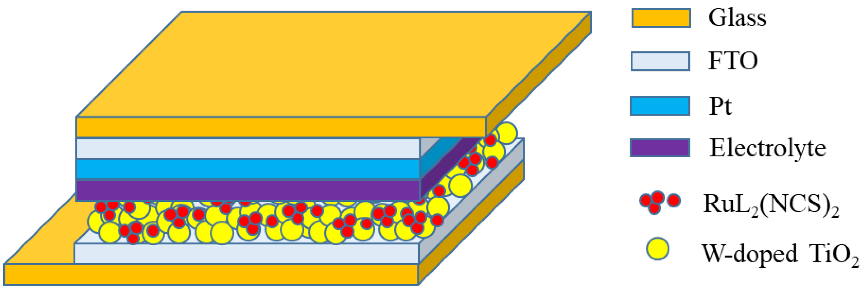
Figure 1 shows the schematic diagram of the DSSC device with FTO/Pt/electrolyte/sensitizing W-doped TiO
2 thin-film/FTO structure. The photovoltaic properties of dye-sensitized solar cells were measured according to a solar cell characteristic measurement system (Newport 94023A, Newport Corporation, Irvine, California, USA). The light source of the solar cell characterization system is a 1000 W xenon lamp equipped with an IR filter and an AM 1.5G filter.
3. Results and Discussion
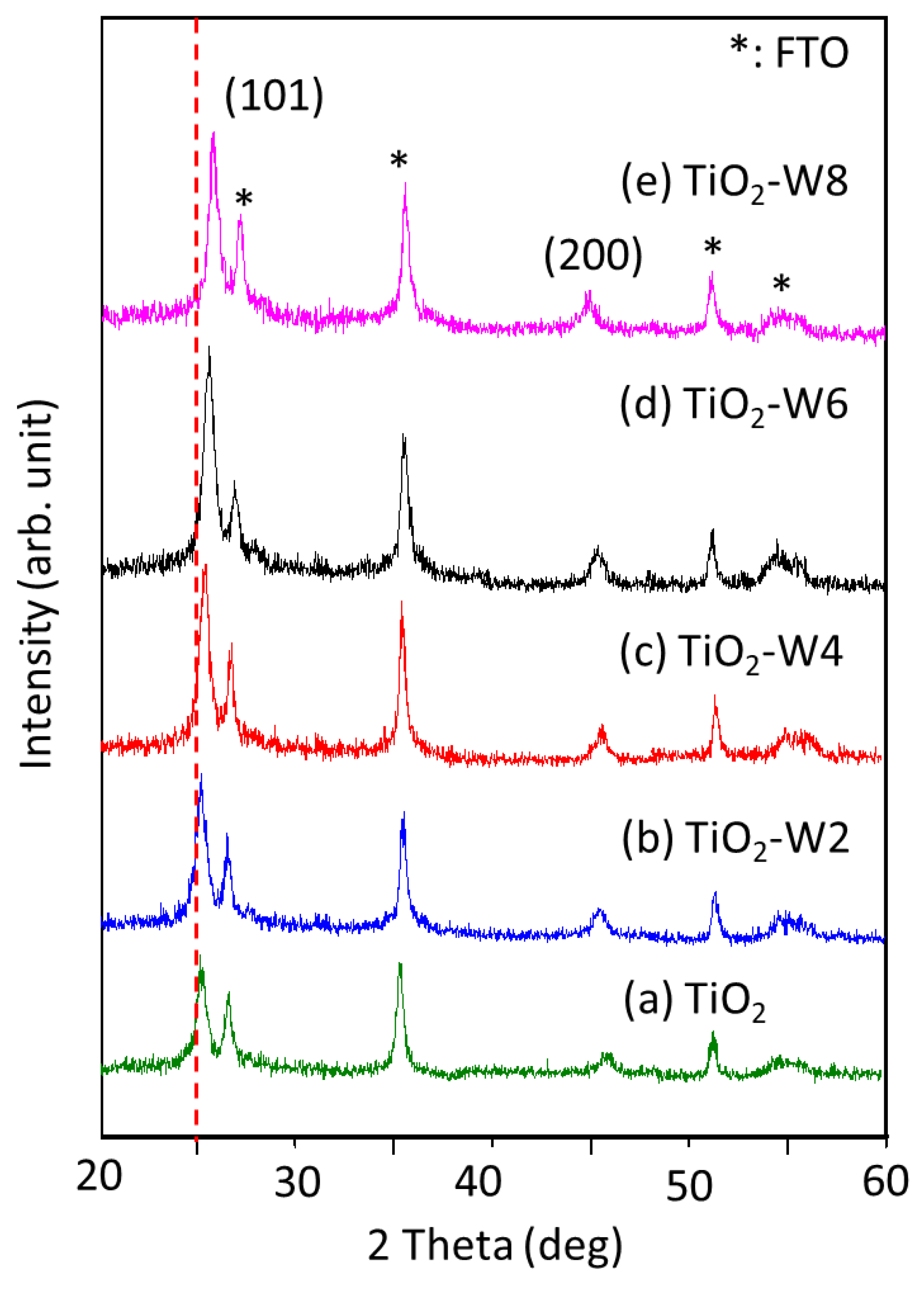
Figure 2 shows the XRD pattern of a W-doped TiO
2 film prepared using the sol–gel method on an FTO-coated glass substrate using rapid thermal annealing at 600 °C for 2 min. XRD results show that the diffraction peaks of all samples conformed to the standard JCPDS (84-1286) had a tetragonal center structure and a (1 0 1) preferred orientation TiO
2 anatase structure and had no rutile phase or any other phase. As the W doping amount increased from 0 at% to 6 at%, the intensity of the (1 0 1) peak of the TiO
2 thin film also increased, but the intensity of the (1 0 1) peak of TiO
2-W8 was smaller than that of TiO
2-W6. In addition, as the W doping amount increased, the (1 0 1) peak of the W-doped TiO
2 film moved to a higher 2θ value. This may be because the doped W ions partially replaced the Ti ions in the TiO
2 crystal or were located in the interstitial positions of the crystal, showing that the TiO
2 unit cell shrinks [
16,
17]. The average crystal size (D) of W-doped TiO
2 thin-film nanoparticles was calculated using the main diffraction peak at 2θ = 25.1° using the Scherrer equation with an interplanar spacing of (1 0 1) [
18].
Here, D is the crystal size, λ is the X-ray wavelength used (0.1540 nm), β is the FWHM of the diffraction peak, and θ is the Bragg angle. The results show that the average grain sizes of TiO2, TiO2-W2, TiO2-W4, TiO2-W6, and TiO2-W8 are 22.5, 23.2, 24.6, 25.6, and 23.8 nm, respectively. From the calculations, it can be seen that doping with W results in a larger crystal size than that with undoped TiO2.
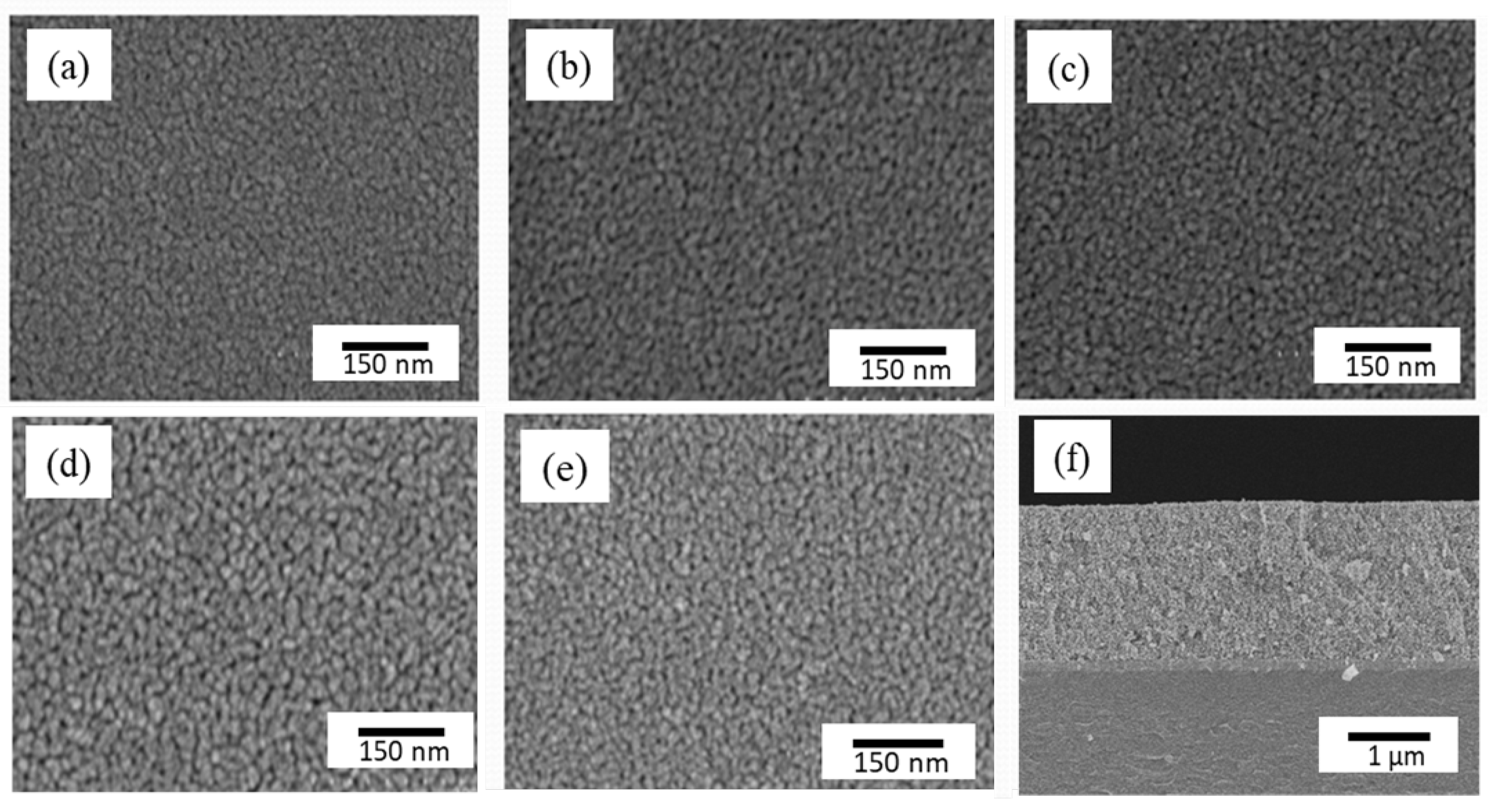
Figure 3 shows the FESEM image of the surface microstructure of a W-doped TiO
2 film.
Figure 3a–e show the surface morphology of the TiO
2 film when the W doping amount increased from 0 at% to 8 at%, while
Figure 3f shows the cross-sectional view of TiO
2-W6. The cross-sectional images show that the thickness of the samples was approximately 2 μm and that all samples had a uniform microstructure with uniform grain size. As the W content increased from 0 at% to 6 at%, the grain size and porosity of the samples increased significantly. However, when the W content further increased to 8 at%, the grain size and porosity of the sample decreased. This phenomenon shows that the increase in the W doping amount had a significant impact on the grain size and porosity of TiO
2 thin films, and the optimal microstructure was achieved at 8 at% doping amount. This may be due to the high concentration of the W element inhibiting grain growth, resulting in a reduction in grain size. The results show that the TiO
2-W6 sample with larger particle size and porosity absorbs more dye when preparing the DSSC working electrode. In order to determine whether there was W element in the as-prepared W-doped TiO
2 thin film, a qualitative analysis of the elemental composition of the sample was performed through EDX spectrum.
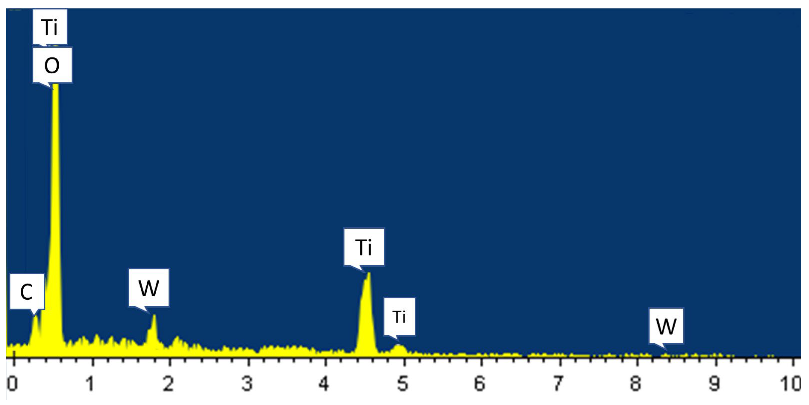
Figure 4 shows a typical EDX spectrum of a 6 at% W-doped TiO
2 thin film, with peaks that can be assigned to Ti, W, and O (the C peak comes from the electric pattern used). It is obvious that W was doped into TiO
2 thin films. Since the EDX spectra of samples with different W doping concentrations are similar, with only slight variations in the W peak, only the spectrum of the 6 at% W-doped TiO
2 thin film is presented.
Table 1 shows EDX results of all samples.
The specific surface area and adsorbed dye amount of W-doped TiO
2 thin films were measured using BET analysis with nitrogen gas adsorption at liquid nitrogen temperature (77 K).
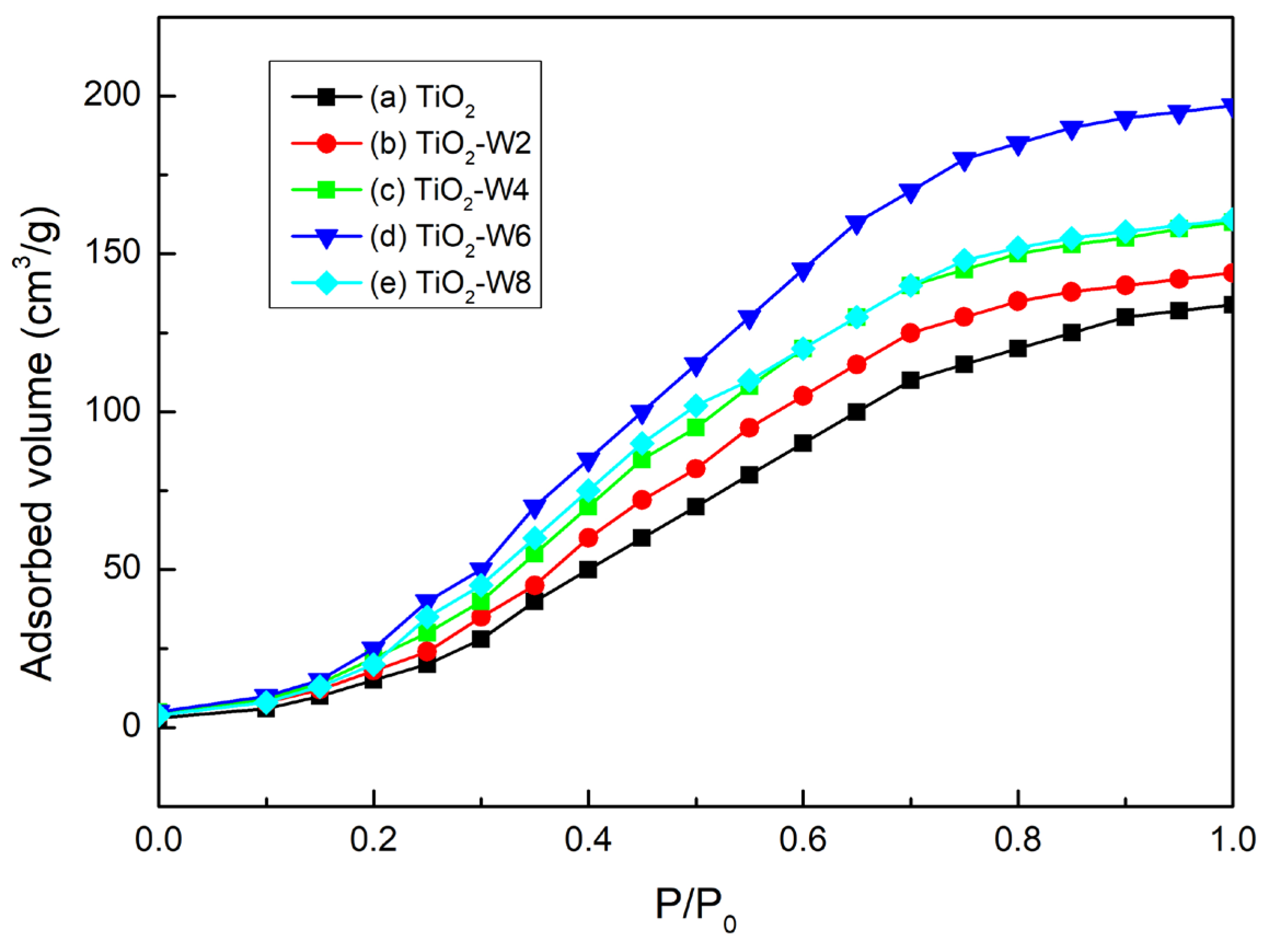
Figure 5 shows the N₂ adsorption–desorption isotherms of the W-doped TiO
2 thin films. The isotherms correspond to type IV curves for mesoporous materials, with an H1-type hysteresis loop. The isotherms indicate that increasing the W content influences the surface characteristics of the W-doped TiO
2 thin films.
Table 2 summarizes the specific surface area, pore volume, pore size, and adsorbed dye amount of the DSSC electrodes fabricated using W-doped TiO₂ thin films. From the results, the specific surface area and the amount of adsorbed dye of the W-doped TiO
2 thin films increased as the W content increased. When the W content was increased from 0 to 6 at%, the specific surface area of W-doped TiO
2 thin films increased from 42 to 58 m
2/g, and the amount of adsorbed dye increased from 2.13 × 10
−8 to 2.65 × 10
−8 mol/cm
2. However, when the W content was further increased to 8 at%, the surface area and adsorbed dye amount decreased to 52 m
2/g and 2.35 × 10
−8 mol/cm
2, respectively. The results show that the TiO
2-W6 sample had the highest specific surface area and adsorbed dye amount. This can be attributed to the significant increase in crystal size and porosity in the TiO
2-W6 sample, providing more surface area for dye molecules to adsorb in the pore structure of the sample [
19]. These data further confirm that the TiO
2-W6 sample, with a pore size of 7.2 nm and a pore volume of 0.22 cm
3/g, provides optimal conditions for dye adsorption, enhancing the efficiency of DSSCs.
To study changes in elemental composition and chemical state, TiO
2-W6 thin films were analyzed by XPS measurements and high-resolution scanning and compared with pure TiO
2.
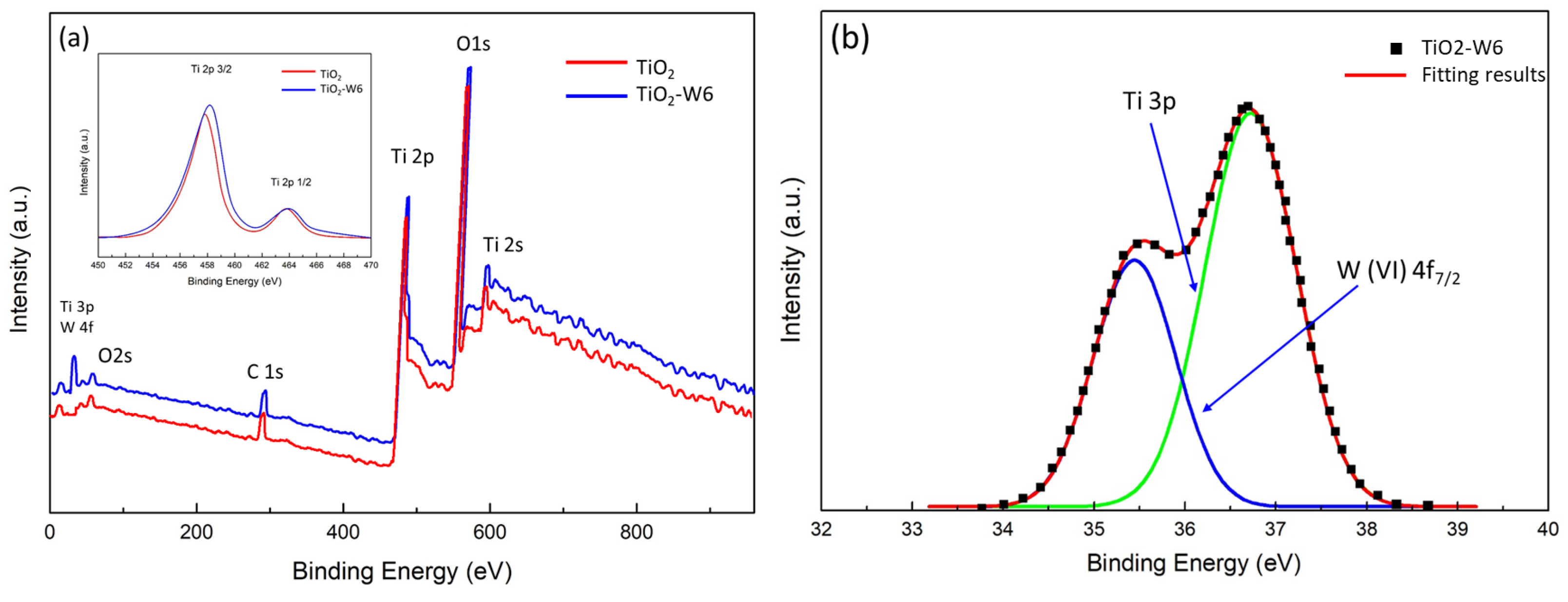
Figure 6a shows a broad spectral scan from 0 to 1000 eV, and the inset shows a high-resolution scan from 450 to 470 eV.
Figure 6b shows high-resolution W4f and Ti3p XPS spectra of TiO
2-W6. In
Figure 6b, the W(VI)4f7/2 peak corresponding to W
6+ is observed at 35.2 eV, indicating that the doping mechanism may be W
6+ ions replacing Ti ions in the crystal [
16,
17]. The chemical state of Ti
4+ (Ti2p) in the TiO
2-W6 film shows significant changes (inset) compared with undoped TiO
2 (inset). The binding energies of Ti2p1/2 and Ti2p3/2 in the TiO
2-W6 film both decreased by 0.6 eV. In addition, the binding energy of O1s in the TiO
2-W6 film sample was 530.8 eV, whereas that of O1s in pure TiO
2 was 529.2 eV. The increase in the O1s binding energy of TiO
2-W6 thin films can be attributed to the existence of oxygen vacancies caused by the doping process [
20]. The presence of oxygen vacancies may be attributed to the replacement of Ti atoms by W ions in the TiO
2 lattice. Since Ti
4+ is occupied by W
6+ in the TiO
2 crystal, W-O-Ti bonds can form in the TiO
2-W6 film. In substitutional doping, foreign atoms replace host lattice atoms, causing structural changes and possibly creating vacancies in the lattice. The changes in O1s peak binding energy observed in the TiO
2-W6 thin film may be related to the substitutional doping caused by the introduction of W dopants into the TiO
2.
The I–V curves for DSSCs fabricated using the W-doped TiO
2 thin film are shown in
Figure 7. The corresponding photovoltaic parameters of DSSCs are summarized in
Table 3. The I–V curve shows the characteristics of a solar cell at different voltages and currents, where Jsc is the current density generated by the DSSC under short-circuit conditions and Voc is the voltage of the DSSC under open-circuit conditions. In addition, the fill factor (FF) is the ratio between the rectangular area of the I–V curve and the maximum possible power area. Conversion efficiency (η) represents the efficiency of DSSCs in converting solar energy into electrical energy, η = (Jsc × Voc × FF)/Pin, the incident light intensity (Pin) is 1000 W/m², and DSSCs are measured under AM 1.5G spectral conditions. From the results, Jsc and Voc increased with the increase in W content. When the W content was increased from 0 to 6 at%, Jsc increased from 13.8 to 20.2 mA/cm
2, and Voc increased from 0.65 to 0.68 V. However, when the W content was further increased to 8 at%, Jsc decreased to 18.4 mA/cm
2. The results show that TiO
2-W6 has optimal solar cell characteristics: Jsc, Voc, FF, and η are 20.2 mA/cm
2, 0.68 V, 68.6%, and 9.42% respectively. A 75% efficiency improvement was found in comparison with that of the non-doped DSSCs. This may be attributed to the increased dye adsorption capacity of the TiO
2-W6 sample with the significant increase in surface area and porosity. The conversion efficiency (9.42%) of the W-doped TiO
2 thin-film DSSCs produced by the sol–gel method in this study is better than that of the DSSCs prepared in previous studies [
13,
14,
15,
16].
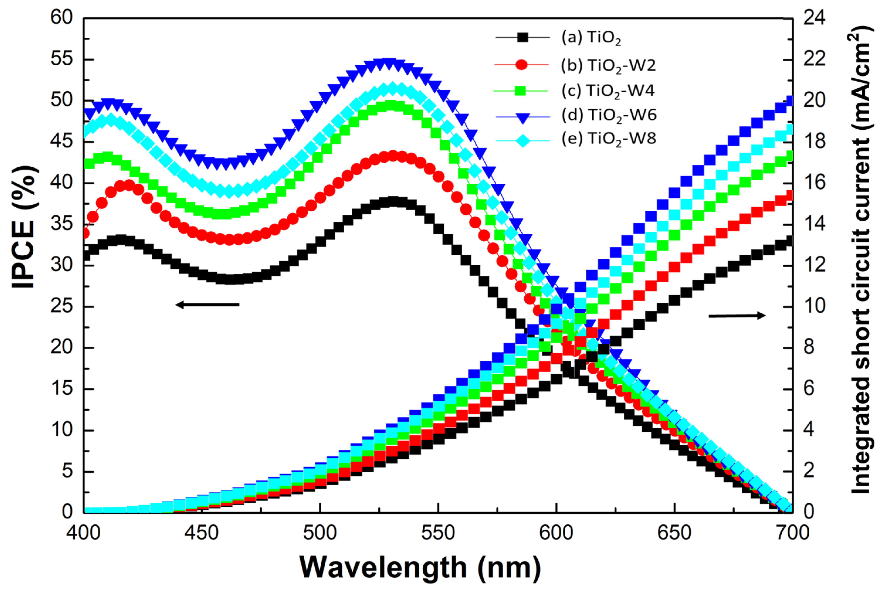
Figure 8 shows the IPCE (%) and integrated short-circuit current (mA/cm
2) of DSSCs with W-doped TiO
2 thin films as a function of wavelength. The IPCE is defined as the ratio of the number of electrons generated by light in the external circuit to the number of incident photons, as follows:
The photocurrent density was determined in the short-circuit state. With the increase in W content from 0 to 6 at%, the maximum IPCE values of DSSCs increased from 35% to 55% at 530 nm. However, the maximum IPCE value (50%) of DSSCs with TiO
2-W8 was smaller than that (55%) of DSSCs with TiO
2-W6 at 530 nm. The higher IPCE value in TiO
2-W6 DSSCs is also consistent with the absorption spectrum of dye-adsorbed W-doped TiO
2 thin films shown in
Figure 7. The integrated short-circuit current of DSSCs with W-doped TiO
2 thin films was calculated based on the IPCE spectra and is also presented in
Figure 8. The obtained integrated short-circuit-current value trends are consistent with the respective I–V curves.
The electron transport at the DSSC interface was measured using electrochemical impedance spectroscopy. The electron transport characteristics of the prepared pure TiO
2 and TiO
2-doped DSSCs doped with different W contents were analyzed when an AC potential of 50 mV was applied.
Figure 9a shows the Nyquist plots of pure TiO
2 and TiO
2 doped with different W contents, where the impedance Re (Z′) is plotted against Im (Z″). The dynamic behavior of electron transport in TiO
2 DSSCs with different W contents was analyzed. The equivalent circuit model was developed from the experimental data as shown in the inset of
Figure 8a. The DSSC impedance spectrum consists of three parts: the series resistance of the FTO substrate (RS), the charge transfer resistance between the counter electrode and the electrolyte (R1), and the charge transfer resistance (R2) between the photoanode and the dye and the electrolyte.
Figure 8a shows that the semicircle in the high-frequency area is unclear. The composite resistance (R2) of the sample decreased as the W doping amount was increased from 0 to 6 at%. This means that the charge transfer resistance at the TiO
2/dye/electrolyte interface decreased by W doping. However, the R2 value of TiO
2-W8 DSSCs is larger than that of TiO
2-W6 DSSCs. The results show that the trend in the R2 value of DSSC is consistent with previous I–V results. The TiO
2-W6 DSSC has the lowest R2 value, which means that the TiO
2-W6 DSSC has a higher electron transfer rate that leads to the highest efficiency and Voc. However, the R2 value of the TiO
2-W8 DSSC is higher than that of the TiO
2-W6 DSSC, so the efficiency (η %) of the TiO
2-W8 DSSC is lower than that of the TiO
2-W6 DSSC [
10,
21].
Figure 9b shows the electrochemical impedance spectra (Bode) in DSSCs doped with TiO
2 with different W contents. The figure shows the peak moving to the left, which indicates that the electron’s lifetime is longer. The electron lifetimes (τn) of DSSCs of TiO
2, TiO
2-W2, TiO
2-W4, TiO
2-W6, and TiO
2-W8 were calculated to be 11.7, 16.9, 22.3, 27.2, and 39.5 ms, respectively. The electron lifetime (τn) in the photoanode was determined using the following relationship derived from the Bode plot of the EIS data, as follows:
where
fmax is the frequency at which the imaginary component of the impedance (Z″) reaches its maximum in the Bode plot. This phenomenon is consistent with the previous Voc.
