1. Introduction
In recent years, renewable energy sources (RESs) such as wind and solar have been playing an important role in the reduction in carbon dioxide emissions [
1], resulting in their increased share in power generation in modern power systems. Maintaining their stability and reliability is challenging due to their intermittent and variable nature [
2]. Semiconductor devices, such as metal oxide semiconductor field-effect transistors (MOSFETs), diodes, and insulated-gate bipolar transistors (IGBTs) are essential components in the control and conversion of renewable energy. However, these devices are prone to permanent damage from over-currents (OCs) and system failures [
3]. Therefore, enabling OC capability in semiconductor devices is an essential requirement in power system design for RESs.
OC situations in RESs can arise from equipment malfunctioning and overloading. Nevertheless, the number of OC events depends on several factors, such as the geographic and economic conditions of the country, grid provider, and weather in that particular area (thunderstorms, lightning, temperature, etc.) [
4,
5]. Protective devices like fuses and circuit breakers can take up to 200 ms and even longer for detecting and clearing the faults [
6]. However, the exact duration of OCs before the semiconductors reach their thermal limits depends on the extent of OC/overloading and varies from one system to another [
7]. Exceeding the rated value of the semiconductor device can result in thermal runaway due to the excessive heat generated. This scenario can lead to the permanent failure of the device.
An OC event causes an increase in the temperature (also referred to as junction temperature) of the semiconductor device. Multiple methods have been investigated and implemented previously to reduce the junction temperature during OCs and steady state. High swings in junction temperature during normal operation decrease the lifetime of the power module [
8,
9,
10,
11,
12]. Therefore, a multitude of researchers have investigated methods to increase the lifetime by reducing (the swing of) the junction temperature. One tested method is the introduction of microchannels below the chip [
13]. Microchannels have shown to be effective in reducing the junction temperature by 60
C with just 0.83 mL/s of water flowing in the microchannels below the chip for a heat flux of 500 W/cm
. However, the exact temperature reduction depends on the amount of heat flux and the location of the microchannels, as illustrated in [
14] for a heat flux in the range of 100–2000 W/cm
[
15,
16,
17]. Another method is using Peltier elements close to the chip, and this has resulted in a reduction in junction temperature of 40
C for 31.5 W of semiconductor losses [
18]. The limitations for Peltier elements arise from the number of Peltier modules needed for high powers and the need for an additional power source driving the Peltier modules. Another design of the power modules is planar which does not have bondwires. Industrial planar power modules technologies include double-sided cooling modules from General Motors [
19], SkiN technology from Semikron [
20,
21], and Siemens Planar interconnect technology [
21,
22,
23]. They have superior performances in terms of having lower thermal resistance during steady state and hence, increased reliability.
Techniques for limiting the junction temperature during transients of a few seconds have been investigated to some extent. One method is the application of microchannel cooling below the chip during OCs for the heat flux up to 2236 W/cm
[
24]. Another method is to add heat-absorbing material below the chip. One such method using combinations of phase change materials (PCMs) with metal containers has been investigated in [
25,
26,
27,
28,
29] for the duration of 3–30 s. PCMs have high latent heat of fusion and low thermal conductivity; hence, the metal containers (being an excellent thermal conductor) in them effectively provide paths of lower thermal resistance such that the heat can be transferred to the PCM. This method suffers from the disadvantage that the junction temperature during steady-state operation is also increased due to the increase in the overall thermal resistance for the heat flow towards the heat sink. The choice of PCMs in such systems is one of the most important aspects as the rate of heat removal depends on the thermal conductivity of the heat-absorbing material(s) below the chip. The thermal conductivity of metallic PCMs is higher than that of non-metallic PCMs (organic and inorganic PCMs including eutectics) [
7,
30]. Consequently, metallic PCMs result in a 20–80
C decrease in temperature as compared to non-metallic PCMs for a heat flux in the range of 85–339 W/cm
in 20 ms [
31]. The thermal response for the heat-absorbing container with PCMs depends significantly on the relative content of the PCMs in question. The optimum relative content of PCM is in the range 30–50%, considering the trade-off between response time delay due to PCM melting and thermal conductivity of overall composite structure [
27,
32,
33]. Another application of PCM with metallic structure is directly in the Si chip substrate for transient applications of 500 W/cm
for up to 100 ms [
34]. Furthermore, another solution for limiting the junction temperature for OCs of 150 ms is presented in [
35] by combining the concept of double-sided cooling and using PCM with metallic structure for a press-pack IGBT module. It resulted in a reduction in junction temperature by 50
C for a heat power of 491.8 W. The authors have not found any additional literature that has provided precise solutions for a few hundred milliseconds of OCs. However, a discussion about potential heat-absorbing materials during OCs is available in [
7,
36]. Metals such as copper, aluminum, gold, diamond, and graphite have been investigated for a heat flux of 400 (W/cm
) during 200 ms. All the proposed solutions discussed above can result in multiple times increased reliability of the semiconductor devices due to decreased temperature swing during OCs, as proved experimentally for the power module with a metallic container for PCM in [
29,
37]. Nevertheless, the exact increase in reliability in terms of cycles to failure depends on the temperature swing and duration of temperature swings [
37,
38,
39,
40]. There is also a research gap in the literature for a comparison of the composite structure made of the metallic container with PCM and just the metallic block. Apart from the heat-absorbing materials, OC capability is also affected by the temperature margins available with semiconductor devices. For example, for the same amount of current (and OCs) and power module structure, SiC devices would be able to handle OCs for a slightly longer duration as compared to silicon devices because the temperature of failure is higher for SiC devices. This will be discussed in detail in the later sections of the paper.
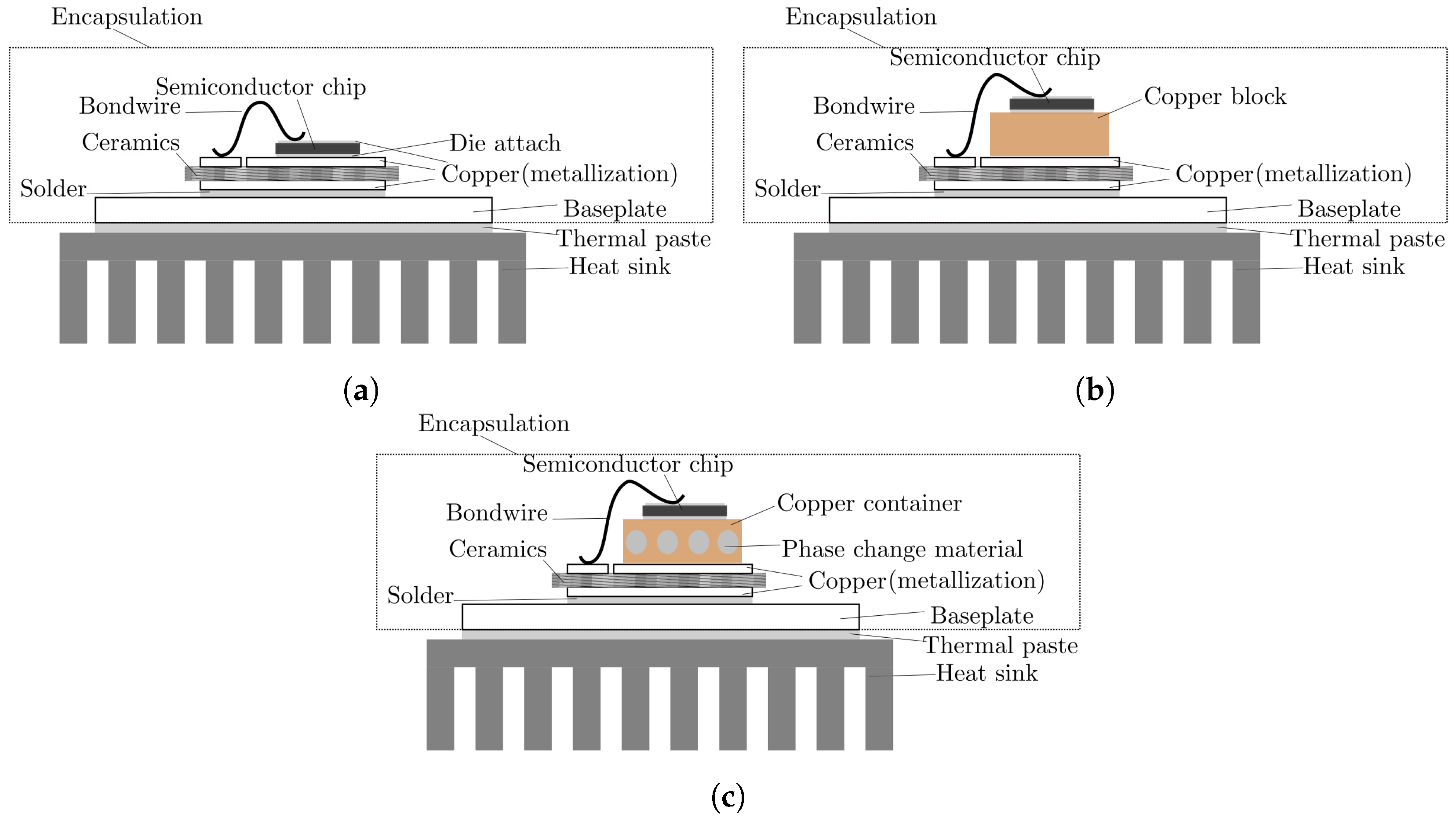
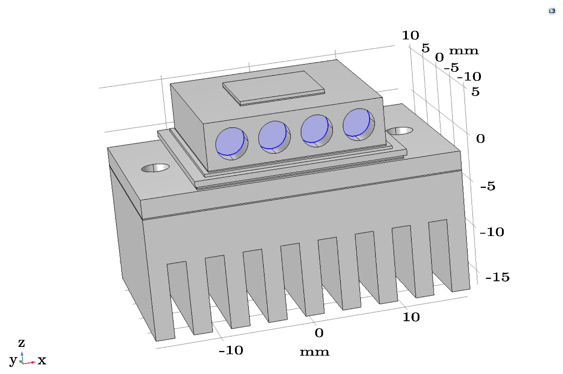
In this article, we are addressing OC capability of standard power modules with the addition of heat-absorbing material below the chip for OCs of two times, three times, and four times the nominal values for a duration of a few hundred milliseconds and seconds. Two types of heat-absorbing blocks are considered below the chip and the analysis is a further extension of the work presented in [
25]. The first structure is a copper block with PCM soldered below the chip, similar to the one presented in [
25]. The second is a copper block soldered below the chip. The two most common applications will be discussed and elaborated, i.e., application of the power devices for inverters and DC/DC converters. Analysis of these applications will help the readers to assess the solutions for OCs for their corresponding applications depending on the power levels and OC duration.
The key contributions of the paper are:
Analyzing the temperature margin with Si and SiC devices in order to enable OC capability.
Comparison of enabled OC capability for Si and SiC devices with modified structures and standard module.
Estimation and comparison of the performance of a copper block and a copper block with PCM for providing OC capability for the duration of a few milliseconds to seconds.
Comparison of thermal performance of Si IGBT and SiC MOSFET power modules for the same amount of current.
The outline of this paper is as follows: In
Section 2, the basic and modified structures of the power modules are discussed. In
Section 3, two times, three times, and four times of OCs have been discussed from a thermal performance perspective.
Section 4 provides a comprehensive discussion of the results and future scope.
Section 5 concludes the article.
3. Analysis and Results
This section explains the differences and the corresponding reasons for the thermal behavior of Si IGBTs and SiC MOSFETs during OCs. The upper limits of the temperature have been assumed to be 175
C for Si [
41] and 250
C for SiC [
7]. Simulations have been performed by means of the finite element method (FEM) in COMSOL for Si IGBTs and SiC MOSFETs for 1200 V power modules. The dimensions for the components of the power module are based on Semikron SKM50GB12T4 [
25] and are shown in
Table 1. The rated value of current is 50 A for the Si IGBT. The power module is a half-bridge with Si IGBTs and anti-parallel diodes. The SiC MOSFET does not need any external anti-parallel diode due to the presence of the intrinsic body diode [
42]. The power module with SiC MOSFETs is assumed to have two SiC MOSFETs in parallel to keep the same geometry as that of the Si IGBT power module for comparing the thermal response of the overall power module.
The current density (300 A/cm
) and ON state resistance (
) of the SiC MOSFETs are taken from the data sheet of CREE MOSFET CPM3-1200-0013A [
43,
44]. They have been estimated for the larger and smaller MOSFETs corresponding to the sizes mentioned in
Table 1. The values for switching energies and intrinsic body diode characteristics are taken from the data sheet E3M0021120K from Wolfspeed [
45] as this MOSFET has similar current and voltage ratings as that of the power module considered for simulations. The rated values of current for larger and smaller MOSFETs are estimated as 263.95 A (
=
m
) and 126.5 A (
=
m
), respectively. Since the converters are designed with safety margins of 30–60% [
25], the nominal values of the current for Si IGBT, SiC larger MOSFETs, and SiC smaller MOSFETs are assumed to be 30 A, 158.37 A, and 75.91 A, respectively. The value of
for SiC MOSFETs varies with junction temperature. The increment in
can be estimated from the data sheet and by extrapolating for 250
C. It increases by 100% from ambient temperature to 250
C. Hence, calculations for losses have been simplified by choosing the average values of
at ambient temperature, 100 and 250
C. The switching frequency (
) is 7.5 kHz for all the cases of Si IGBTs and SiC MOSFETs. The DC link voltage is assumed to be 600 V (half of the rated voltage). The results and discussions are presented in the further sections for nominal current values, two times of OC, three times of OC, and four times of OC. Hereafter, an OC of two times the nominal current will be denoted as 2 OC. Correspondingly, OCs of three and four times the nominal current will be denoted as 3 OC and 4 OC, respectively. The OC is applied at 60 s in all the simulations so that the power module reaches a steady state before 60 s in all cases.
The physics used in COMSOL is ’Heat Transfer in Solids’. The ambient temperature is assumed to be 35
C. Further, a subnode for the PCM is added to the model to simulate the impact of PCM. The phase change phenomenon in PCM and sensible heating provide thermal capacity during OCs and is modeled as [
32].
where
is the total thermal energy stored in the PCM,
is the melting point,
is the melting enthalpy,
and
are the specific heat capacities in solid and liquid state, and
and
are the initial and final temperatures of the PCM, respectively.
The transition during the phase change from solid to liquid is modeled as (
2) [
46]. This complete model of power module with PCM for Si IGBTs is taken from [
25] and has been validated experimentally in [
25].
wherein
denotes the density,
denotes the fraction of the amount of material in a physical state (solid or liquid), and subscripts ‘s’ and ‘l’ denote the parameters for the solid and liquid states, respectively.
All the boundary surfaces in contact with the ambient are thermally insulated, except for the heat sink, in order to replicate a real operating condition inside the power module.
The physical properties of the materials used in the simulations are listed in
Table 2. The PCM used for the Si power module is LM108; meanwhile, for SiC, it is Lithium. The criteria for choosing these PCMS are that their melting point is in the range of operation of the devices, high melting enthalpy, and high thermal conductivity in the case of Lithium. The thermal conductivity of PCMs in the liquid state has been assumed to be four times higher due to the increased convection in the liquid state as compared to the solid state, which has been verified in the experiments in [
25] for LM108.
3.1. OC Capability for Inverter Drive
This subsection discusses the thermal performance of the leg of an H-bridge with Si IGBTs and SiC MOSFETs in inverter operation. The losses for Si IGBTs and the diodes are calculated using the application notes from Infineon [
55] and Dynex [
56]. The conduction losses and switching losses for IGBTs and the anti-parallel diodes are given by Equations (
3)–(
6).
The conduction losses of an IGBT are given by
where
m is the modulation index,
is the power factor,
is the on-state threshold voltage of the IGBT,
is the peak collector current, and
is the on-state resistance of the IGBT.
in which
and
the turn-on and turn-off energies at
,
is the switching frequency,
is the DC link voltage,
is the rated saturation voltage of the IGBT,
is the nominal value of current of the IGBT, and
is the output current.
For freewheeling diode of the IGBT, the conduction losses are given as
where
is threshold voltage of the diode and
is the on-state resistance of the diode.
The switching losses of a diode are given by
wherein
is the reverse recovery energy of the diode at
.
Losses for the SiC MOSFETs are calculated using the application note from Infineon [
57]. The losses in the SiC MOSFETs and the body diodes are over-estimated if reverse conduction of the SiC MOSFET channel is not taken into account [
58]. For the SiC MOSFETs, the body diode conducts only if the voltage drop across the SiC MOSFET channel
is greater than the threshold voltage of the body diode [
59,
60]. If the voltage across the SiC MOSFET channel is less than the threshold voltage of the body diode, the SiC MOSFET channel conducts in the reverse direction. For simplicity, the SiC MOSFET channel resistance is assumed equal in both forward and reverse conduction. Since the current flowing through the SiC MOSFETs is sinusoidal in the inverter, the maximum voltage drop across the MOSFET channel is when the peak current flows. The voltage drop for 4 OC at the current peak (633.5 A) is 3.1 V, which is less than the threshold voltage (4.4 V) of the body diode of the SiC MOSFET. Hence, it is assumed that the entire current is flowing through the MOSFET channel in reverse conduction for all the cases discussed further in the paper. This simplification causes a slight overestimation of the losses for the SiC case. The MOSFET losses would be equally divided between the upper and lower MOSFETs due to the reverse conduction. The conduction and switching losses in the SiC MOSFETs are given by (
7) and (
8).
where
is the on-state resistance of the MOSFET and
is the rms value of the load current.
in which
and
are the turn-on and turn-off energies of the SiC MOSFET for the particular value of current.
The switching losses of the body diodes in the SiC MOSFETs are negligible (if the body diodes conduct) as compared to the conduction losses [
61]. The value chosen for
and modulation index (
m) is 0.9 for all the inverter cases. The losses calculated for both Si and SiC devices are time-averaged for switching and conduction losses.
This subsection discusses three cases of inverter operation. First, the thermal performance of the power modules with Si IGBTs and SiC MOSFETs are discussed and compared for their nominal current ratings, 2 OCs, 3 OCs, and 4 OCs. Second, the thermal performance is analyzed for the SiC MOSFET power module with nominal current ratings and OC values of the Si IGBT power module. Third, the duration of OCs is investigated without reaching the upper limit of temperatures with Si and SiC power modules when the initial temperatures are approximately 100 C. These analyses would provide a comparison and insight into the current capabilities and OC capabilities of the Si IGBTs and SiC MOSFETs.
One point to note is that the heat sinks can be selected in various ways depending on the application and power density [
62,
63]. Due to high current density for SiC MOSFETs, the heat sink is designed in such a way that the average temperature of the MOSFETs for the nominal current values is limited to approximately 100
C. However, in order to make a fair comparison between Si and SiC devices, the same thermal design is chosen for the Si power module. It results in an over-designed cooling circuit for the Si power module, leading to very low temperatures for nominal current during the steady state. Since the losses in the Si power module are lower than in the SiC power module for their corresponding rated values and because the maximum temperature is higher for the SiC device, the heat sink can be smaller for the Si power module than the one required for the SiC power module. It would result in a temperature that would be in the recommended range of the data sheet of the power module.
3.1.1. Nominal Ratings of the Devices
Using (
3)–(
8), the losses for the Si IGBT and the SiC MOSFET power modules are calculated and given in
Table 3 and
Table 4, respectively. The losses for both Si and SiC devices are calculated for nominal values, 2 OC, 3 OC, and 4 OC. The losses of the SiC MOSFETs are higher as compared to Si IGBTs for the corresponding nominal current, 2 OC, 3 OC, and 4 OC. It is due to the fact that the current values for the larger and smaller SiC MOSFETs are approximately 5 times and 2.5 times higher than that of the Si IGBT, respectively. The total current in the SiC MOSFET power module (small and large MOSFET combined) is approximately 7.8 times higher as compared to the Si IGBT due to the fact that the SiC power module can handle a higher current and the area of the diode is being used as a MOSFET as well.
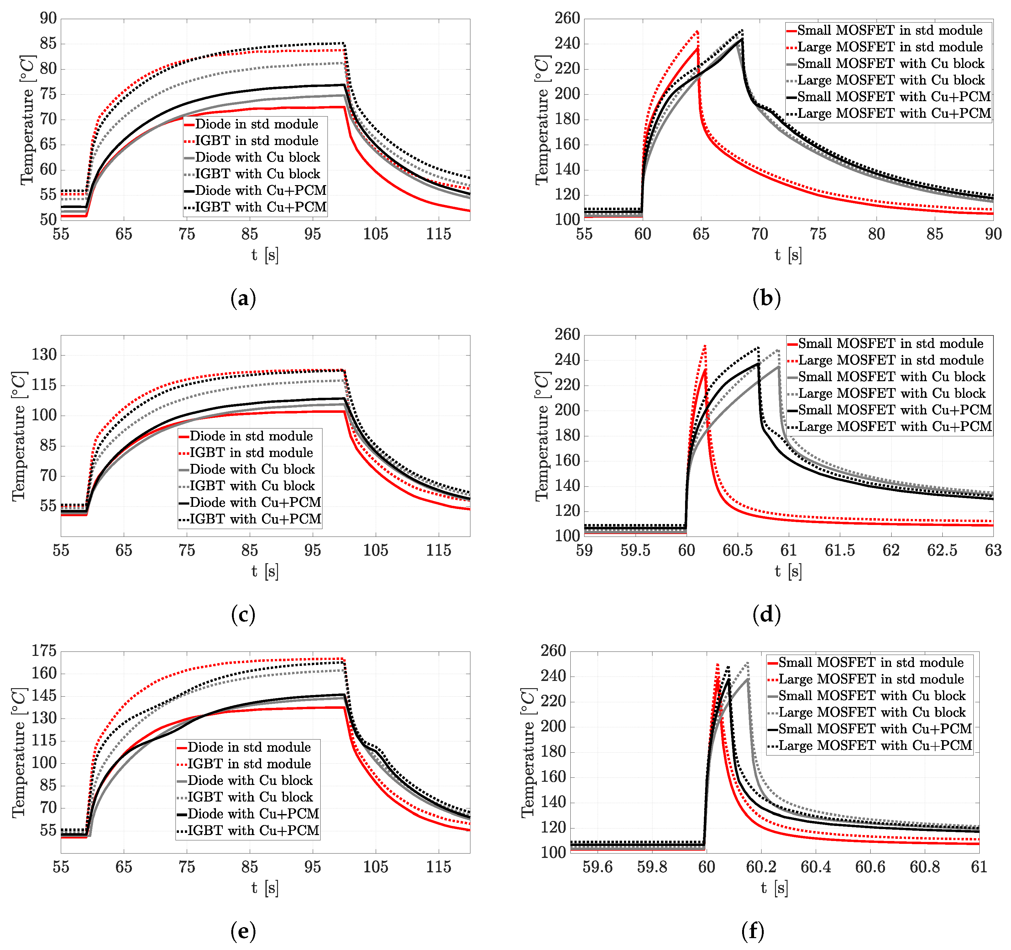
Figure 3 shows the average temperature of the Si and SiC devices under various OCs.
Figure 3a,c,e shows the average temperatures of the diode and the IGBT as above while
Figure 3b,d,f shows the SiC MOSFETs. It should be kept in mind that the values of OCs are different for Si IGBTs and SiC MOSFETs. For instance, the value of 2 OC for Si IGBT is 60 A, while it is 316.75 A for SiC larger MOSFET. This is due to the difference in rated values of current, current capability, and thermal properties of Si and SiC devices.
It can be observed that the temperatures of the Si IGBT and diode in their nominal operation are lower as compared to the nominal operation of the SiC MOSFETs. This is due to the higher losses in SiC devices at much higher values of currents. The temperatures of the IGBTs in the silicon power module with a copper block and a copper block with PCM are between 81 and 83
C, between 117 and 123
C, and between 162 and 170
C for 2 OC, 3 OC, and 4 OC, respectively. The OCs are applied for 40 s since the temperature reaches a steady state in all OC cases of the Si IGBT power module. For
Figure 3a, the temperature of the devices has not reached to melting of the PCM and due to the lesser thermal conductivity of PCM as compared to the copper; there is a difference of 3.95
C in the final temperature of the IGBT with copper clock and copper block with PCM. The amount of PCM melted in 40 s for 3 OC is 20% while it melted completely in 16 s for 4 OC. One important thing to observe is that the temperature of the IGBT does not reach 175
C even for the standard module, which means that the device would not fail for standard modules. However, there is a reduction in the temperature of the IGBT during OCs for the modified structures of the power module. The reduction in the temperature of the IGBT is due to two factors. First, the copper block below the chip acts as a heat spreader as shown in the case of 2 OC in
Figure 3a. Second is the absorption of the heat during OCs by the melting process of PCM when the temperature of the IGBT reaches the melting point (108
C) of the PCM LM108. These two factors are acting simultaneously during 3 OC and 4 OC, as shown in
Figure 3c,e. This reduction in the temperature of IGBT can result in increased lifetime of the Si power module.
The OC durations for the SiC MOSFETs are increased significantly before the temperature of the larger SiC MOSFETs reaches 250
C, as shown in
Figure 3b,d,f. For 2 OC, the temperature reaches 250
C in 4.7 s for the larger SiC MOSFET as shown in
Figure 3b, and the duration of OC is increased by using the copper block and the copper block with PCM to 8.6 s and 8.5 s, respectively. The PCM melted completely in 7 s. The temperature is lower with the copper block until 5 s after OC is applied; after 5 s, the performance is almost identical until the temperature reaches 250
C. The duration for 3 OC increases from 185 ms for the standard module to 900 ms with the copper block and to 700 ms with the copper block with PCM. The fraction of PCM melted for this case in 700 ms is 24%. The temperature of the larger and smaller MOSFET is lesser with copper block as compared to copper block with PCM at any point of time during OC. Similarly, the OC duration increases from 40 ms to 150 ms for 4 OC for the power module with copper block and 86 ms for copper block with PCM for the larger MOSFET. The PCM is not melted (0.65% melted) in 86 ms since the thermal conductivity of the PCM is much lower than that of copper but the temperature reaches 250
C in the same duration. One point to be noted is that there is no significant difference between the thermal performance of the copper block and the copper block with PCM for 2 OC, while the performance is better with copper for 3 OC and 4 OC, resulting in a higher preference for the copper block due to the ease of making this structure.
3.1.2. SiC MOSFETs with the Current Ratings of Si IGBTs
This subsection compares the performance of the SiC MOSFET power module with the current values (nominal and OCs) of the Si IGBT power module. As discussed in
Section 3.1.1, the performance of Si and SiC power modules with a copper block is almost identical to the ones with a copper block with PCM. Accordingly, the power modules with only a copper block are discussed further in this subsection and in
Section 3.1.3.
The total current in the SiC power module is proportionally distributed between the large and small SiC MOSFETs according to their areas. The losses in the SiC MOSFETs are calculated using (
3)–(
8), with the same procedure as described in the previous subsection.
Table 5 shows the combined losses of the large and small SiC MOSFETs. It is important to note that the combined losses of both the MOSFETs in the SiC power module (
Table 5) are significantly lower compared to the combined losses of the Si IGBT and the Si diode in the Si Power module (
Table 3).
Figure 4 shows the difference in the temperatures of all the devices for 2 OC, 3 OC, and 4 OC.
Figure 4a shows the temperature of the IGBT and diode while
Figure 4b shows the temperature of SiC MOSFETs for all OCs. As shown in
Figure 4, the temperature of the MOSFETs (about 40.7
C) is lower than the Si IGBT and diode (52–55
C) for the nominal current value of IGBT (30 A). Similar observations can be made when OCs occur in both the power modules (Si IGBT and SiC MOSFET). The difference in the constant values of the temperatures reached between the larger SiC MOSFET and Si IGBT are 33.26
C, 60.8
C, and 95
C for 2 OC, 3 OC, and 4 OC, respectively. The difference in temperature of the Si IGBT and the diode increases as the OC value increases. It can be concluded that the SiC power module with a copper block has a lower temperature and better thermal performance than the Si power modules with a copper block for the same values of current in all the described cases. This could result in a longer lifetime and higher reliability of the SiC power module.
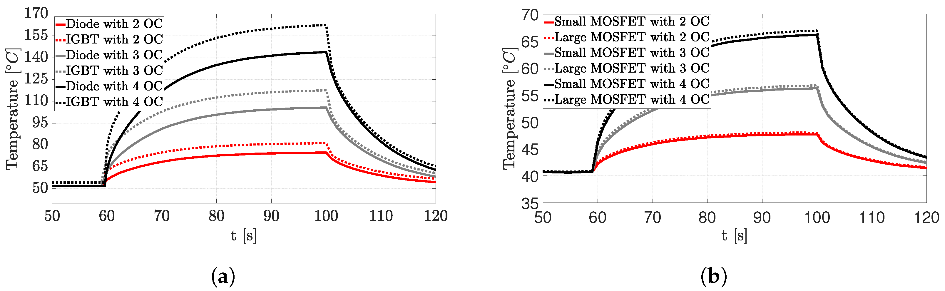
3.1.3. 100 °C Chip Temperature before OCs
In this section, OC capability is discussed for the case when the temperature of the MOSFETs and IGBTs is about 100 °C. Before 60 s, the temperature of MOSFETs is approximately 100 °C during the steady-state operation for 0.95 times the nominal current values (150.46 A for larger MOSFET and 72.11 A for smaller MOSFET), as shown in
Figure 5b; meanwhile, the current value for the IGBT is 2.5 times the nominal current value (75 A), as shown in
Figure 5a. The total losses (conduction + switching) with 150.46 A for the larger MOSFET and 75 A for the smaller MOSFET are 66.04 W and 31.65 W, respectively. Meanwhile, with 75 A for the IGBT and the diode, the losses are 76 W and 15 W, respectively.
When the current in the Si power module is changed from 75 A (2.5 times nominal value) to 120 A (four times nominal value) for 40 s, the temperature reaches a steady state at 163 °C, as shown in
Figure 5a. When 2 OC is applied to the SiC MOSFETs with an initial steady state at current of 0.95 times the nominal value, the temperature reaches 250 °C in 9 s for 3 OC and 1 s for 3 OC, while this duration is 170 ms for 4 OC. The difference in the durations of OCs for Si IGBTs and SiC MOSFETs is because of the differences in the losses corresponding to significantly different current values. These observations can be made from
Figure 5.
3.2. DC/DC Converter
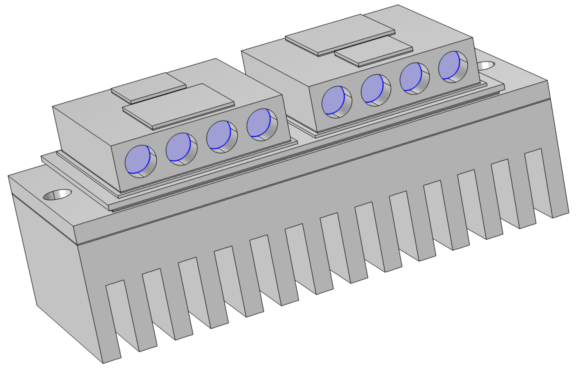
In this section, the thermal performance of the power modules with one device is discussed. Consequently, the heatsink, baseplate, and DBC are dimensioned to half and the device is symmetrically located as shown in
Figure 6. The assumption is that the device is being utilized in a DC/DC converter with a duty cycle of 50% with no blanking time. Hence, there is no need for a freewheeling diode in this case. The switching frequency is kept the same as in the previous case of the inverter at 7.5 kHz. The calculation of losses of the Si IGBT and the SiC MOSFET is performed using the general equations for the IGBT and MOSFET using (
9)–(
11). The general equations for IGBT losses are given in [
55,
56] and for the MOSFET in [
57]. The values of switching energies for the IGBT have been taken from the data sheet of the IGBT power module from Semikron SKM50GB12T4 [
25] and for the MOSFET, they are estimated by interpolation using the data sheet of the SiC MOSFET in E3M0021120K by Wolfspeed [
45].
The conduction losses of an IGBT are given by
where
and
are the average and rms values of collector current.
The conduction losses for a MOSFET are described as
where
is the rms values of the drain current. The switching losses for the IGBT and MOSFET can be shown as
where
and
are the turn-on and turn-off energies for the IGBT and MOSFET for their corresponding current values.
Table 6 and
Table 7 show the total losses for the Si IGBT and the SiC MOSFET, respectively, for nominal current, 2 OC, 3 OC, and 4 OC.
Figure 7 shows and compares the temperatures of the Si IGBT and SiC MOSFET for their nominal current and various OCs.
Figure 7a,c,e shows the Si IGBT and
Figure 7b,d,f shows the SiC MOSFET. The temperature for nominal current with a copper block is lesser by 5
C for Si IGBT as compared to the standard module and the module with copper with PCM. One possible reason for this could be that the module with the copper block has better heat spreading below the chip as compared to the module with copper with PCM because of high thermal conductivity of copper as compared to the PCM. Similarly, the differences in temperature for SiC MOSFET with copper block and copper block with PCM as compared to the standard power module are 7.3
C and 2.67
C, respectively.
For the Si IGBT, the temperature is approximately 80
C for nominal current. During 2 OC in
Figure 7a, the temperature reaches a steady state at about 147
C for the copper block with PCM while it is about 142
C for the copper block, as compared to 155
C in a standard module. The advantage of using the copper block and the copper block with PCM is that the temperature swing is reduced during 2 OC but the duration, which it can withstand before it reaches 175
C, is not affected. However, the reduction in temperature could lead to an increased lifetime of the power module. For 3 OC in
Figure 7c, the duration of OC is increased from 1 s for the standard power module to 6 s with copper block and to 5.5 s with copper with PCM before the temperature reaches 175
C. The PCM melted completely in 32 s for 2 OC and 5 s for 3 OC. Similarly, for 4 OC in
Figure 7e, the duration of OC is increased from <50 ms for the standard power module to 900 ms for copper block and to 800 ms for copper block with PCM before the temperature reaches 175
C. Approximately 27% of the PCM melts during 4 OC.
For the SiC MOSFET, the temperature is approximately 100
C for the nominal current. During 2 OC in
Figure 7b, the temperature reaches 250
C for the copper block in 4.9 s and for the copper block with PCM in 5 s, while the temperature reaches 250
C in 0.75 s for the standard power module. Approximately 70% of the PCM melted in 5 s. For 3 OC in
Figure 7d, the duration of the OC is increased from 30 ms for the standard power module to 210 ms with the copper block and to 120 ms s for the copper block with PCM before the temperature reaches 250
C. Similarly, for 4 OC in
Figure 7f, the duration of the OC is increased from 10 ms for the standard power module to 20 ms with the copper block and to 17 ms with the copper with PCM before the temperature reaches 250
C. For 3 OC and 4 OC, the PCM almost did not melt.
An important point to note is that the performance of the power module with the copper block is almost the same or slightly better. It is because the duration of OCs is shorter with higher heat per unit area for the module with one device as compared to the H-bridge module and hence, PCM is not melted completely for 3 OC and 4 OC for SiC and 4 OC for Si device because of its lower thermal conductivity. In addition, copper block is easier to utilize than the copper block with PCM, therefore, using the copper block might be a preferable solution for increasing the OC capability for all the cases discussed above for Si and SiC devices.
4. Discussion and Future Directions
In
Section 3, the thermal performance of modified power modules is discussed and compared with standard power modules in terms of OC durations and the temperature of the chips (Si IGBT, Si diode, and SiC MOSFETs). OCs of 2 times, 3 times, and 4 times are analyzed for different cases. The upper limit of temperature for Si devices is 175
C and for SiC devices, it is 250
C
In
Section 3.1, the modified structures are compared with the standard power module for the inverter application for up to 4 OC. The Si IGBT power module consists of an IGBT and anti-parallel diode for freewheeling while for the SiC MOSFET power module, no freewheeling diode is needed due to the presence of an intrinsic body diode in the SiC MOSFET. Accordingly, two MOSFETs are assumed to have the exact same dimensions as that of the IGBT and diode in the Si IGBT power module.
The structures with a copper block and a copper block with PCM have enabled OC capability for the SiC MOSFET power module while the temperature swing is reduced for the Si IGBT power module. The conclusions of
Section 3.1.1 and
Figure 3 are tabulated in
Table 8 and
Table 9 for the heat fluxes in the range from 27 to 185 W/cm
for the Si IGBT, 13–72 W/cm
for Si diode and 85.85–1198 W/cm
for SiC MOSFETs. The values for the standard module have been highlighted in red. A duration of >40 s implies that the temperature has reached steady state values for that particular OC and that the temperature would not increase further even if the duration of OC is increased.
Section 3.1.2 discusses the OC capability and its duration for the SiC MOSFET power module with the current values of the Si IGBT power module. The losses for SiC MOSFETs (and hence, the chip temperatures) are lesser than Si IGBT devices for the same values of current (
Table 3 and
Table 5). As seen in
Figure 4, the temperature at any point of time (before and after OC) is lower for the SiC MOSFET power module as compared to the Si IGBT power module. All these facts indicate that SiC MOSFETs could be more advantageous as compared to Si IGBT for reducing the losses and increasing the current capability for the identical configuration of the power modules.
Section 3.1.3 discusses the OC capability and its duration when the chip temperature before OC is 100
C.
Table 10 has the conclusions for various OCs of both devices.
Finally, in order to make a one-to-one comparison of the Si IGBT and the SiC MOSFET, power modules with only one Si IGBT and one SiC MOSFET are considered for a DC/DC converter application. In this power module configuration, the copper block and the copper block with PCM significantly increase the current capability in terms of duration of OC for all the OCs for both the devices before reaching their corresponding upper limits of temperature, except for Si IGBT with 2 OC, as the temperature did not reach the limit even after 40 s.
Table 11 and
Table 12 conclude
Section 3.2 for the heat fluxes in the range from 86 to 589 W/cm
for the Si IGBT and 126–2235 W/cm
for the SiC MOSFET.
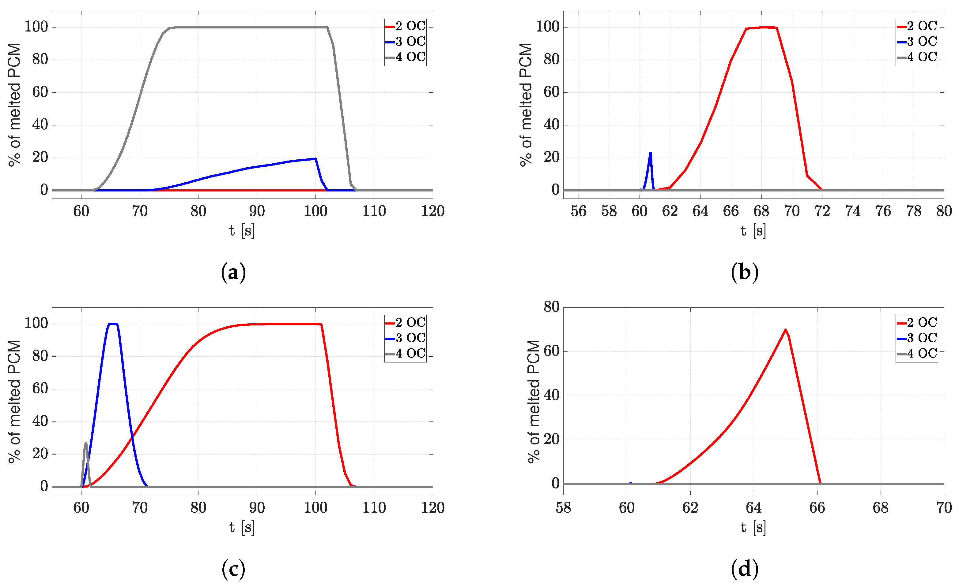
The conclusions of
Section 3 are tabulated in
Table 13. The fraction of melted PCM (in %) is shown in
Figure 8 for all the cases discussed in the paper.
In
Figure 8a, for the Si IGBT in inverter application, PCM does not melt for 2 OC because the temperature of the IGBTs and diodes does not reach the melting point of the PCM LM108. For 3 OC, the temperature of the IGBTs reaches above the melting point of the PCM but the amount of heat available during the OC is not sufficient to melt the PCM completely. For 4 OC, the amount of heat available is enough to completely melt the PCM in 15 s. Similarly, for the Si power module operating in the DC/DC converter application for 2 OC and 3 OC in
Figure 8c, the amount of heat available during OC is sufficient to melt the PCM completely. For 4 OC, the the amount of heat to melt the PCM is available but the temperature of the IGBT reaches the upper limit of the temperature when the fraction of melted PCM is approximately 27%. For the SiC power module for inverter application in
Figure 8b, the amount of heat energy available during 2 OC is sufficient to melt the PCM (Lithium) in 7 s. For 3 OC and 4 OC, the temperature of the MOSFETs reaches the upper limit when the amount of PCM melted is 22.6% and 0.65%, respectively. On the other hand, the temperature of the MOSFETs reaches the upper limit in 5 s for 2 OC for the DC/DC converter application in
Figure 8d, when the melted PCM is 70%. On the other hand, the PCM does not melt for 3 OC and 4 OC.
It can be concluded from the above discussion that the performance of the copper block is better or almost identical to that of the copper block with PCM in terms of limiting the temperature and increasing the OC duration for the cases until a few seconds of OC. The reason to this is that copper has a higher thermal conductivity. However, the copper with PCM showed slightly better performance than the copper block for 2 OC in the SiC MOSFET (
Figure 3b) for half-bridge power modules until 5 s. Nevertheless, the exact difference between the performance of both modules depends on the duration of the OC, the highest temperature limit, and the amount of heat. Adding just a copper block is easier to manufacture and connect to the power module as compared to manufacturing a copper block with PCMs. Hence, it is recommended to use only a copper block below the chip rather than a copper block with PCM. However, the application of PCMs with modified technology such as making composite and porous structures using highly thermally conducting materials like graphene might have the potential to even improve the electrical, thermal, and mechanical performance of the power module [
64,
65,
66,
67]. It should be kept in mind that the proposed power module structure has more weight as compared to the standard power module design. Consequently, the feasibility of the proposed structure would depend on the application. If weight is an important aspect, such as in aerospace and EV applications, adding more chips in parallel might be a preferable option. However, adding more chips is more expensive as compared to adding a simple copper block or copper block with PCM. However, for applications where the weight and volume of the converter are not the limitations, such as substations in power systems or HVDC converters, the suggested power module structures with copper or copper with PCM might be preferable, as it would be cheaper than adding more chips in parallel. However, the increase in the weight of the converter would be small.
Another aspect of the modification in the power module that should be considered is its impact on the lifespan of the power module. The factors affecting the lifespan of power modules are junction temperature swing, its duration, and the number of cycles [
37,
38,
39,
40]. The proposed structure leads to a decrement in the temperature swing during OCs for the inverter and DC/DC converter application with the steady-state temperature almost the same or lower than the standard power module, as discussed in
Section 3.1 and
Section 3.2. Nevertheless, the impact of the addition of the copper block (with or without PCM) on lifespan should be quantitatively and qualitatively analyzed by thermomechanical investigations.
Since the copper block below the chip is an addition in the path of heat flow in the power module and increases the thermal resistance during the steady state, the chip temperature in the steady state with the nominal current would be higher than the standard module as observed for the diodes of Si IGBT module. One solution for this increase in the junction temperature is to add heat-absorbing material on the top of the chip instead. This arrangement will not increase the thermal resistance during steady state and would be able to provide heat capacity during OCs. If this heat-absorbing material would be electrically conducting, the material itself can be used to provide the electrical connection to the external circuit and would result in the removal of bond wires. This structure without bond wires is also called a planar module. The elimination of bond wires and the reduction in chip temperature will result in an increased lifetime and reliability of the power module. Other interesting materials which could be utilized instead of copper are diamond and graphite. Diamond can only be placed below since it is an electrical insulator while graphite can be placed below and above since it is electrically conducting. However, connecting graphite to the semiconductor chip might be a complicated procedure.


