Article

A Flyback Converter with a Simple Passive Circuit for Improving Power Efficiency

Division of Electronic Engineering, Jeonbuk National University, Jeonju 54896, Republic of Korea
Energies 2024, 17(18), 4729; https://doi.org/10.3390/en17184729
Submission received: 15 August 2024 / Revised: 19 September 2024 / Accepted: 20 September 2024 / Published: 23 September 2024

Abstract

:
This paper proposes an effective method to improve the power efficiency of the flyback converter in the continuous conduction mode (CCM). The proposed converter uses a simple passive circuit to reduce the switching power losses. The current through the output diode can be shifted to a new branch where one diode, one inductor, and one auxiliary winding of the transformer are included. The output diode current can be reduced to zero for the zero-current switching of the output diode. The additional inductor is used to control the changing rate of the additional diode current to reduce the reverse-recovery current. Keeping the simplicity of the passive method, the proposed converter improves the power efficiency compared to the conventional converter. The circuit configuration and the operation principle are described. The design considerations are presented, including the simulation verification. The experimental results for a 45 W prototype are discussed to evaluate the performance of the proposed converter. The proposed converter has achieved a power efficiency of 93.5% for the rated load condition, improving the power efficiency. The applications of the proposed converter are also discussed for the future research directions.

1. Introduction

The flyback converter has been widely used for low-cost power supplies due to its simple circuit structure [1,2,3,4]. It has been utilized for various applications such as photovoltaics [1], portable devices [2], solid-state lighting [3], and motor drive systems [4]. Figure 1 shows the circuit diagram of the conventional flyback converter. To increase the power density, the flyback converter should operate with a high switching frequency. However, it suffers from the switching power losses as the switching frequency increases. In general, the switching power losses of the flyback converter are caused by the power switch Sp and the output diode Do. The energy stored in the transformer leakage inductor Llk mainly causes the power losses. The reverse-recovery current of the output diode additionally increases the power losses, which deteriorates the power efficiency of the flyback converter.
To reduce the switching power losses, various switching techniques have been proposed for the flyback converter [5,6,7,8,9,10,11,12,13,14,15,16,17,18,19,20]. The power efficiency can be improved by making the flyback converter operate in the boundary conduction mode (BCM) [6,7,8,9,10]. The flyback converter in the BCM operates at the boundary of the continuous conduction mode (CCM) and the discontinuous conduction mode (DCM) [6]. The valley switching is accomplished by varying the switching frequency of the flyback converter in the BCM [7]. It enables the output diode to be turned off at zero current in the flyback converter. The output diode operates by minimizing the turn-off switching loss [8]. However, the valley switching technique requires a wide range of switching frequencies to regulate the output voltage [9]. As the switching frequency changes according to the output load conditions, the closed-loop control is not easy to design [10]. As the switching frequency decreases, the current stresses on the switching devices increase with high conduction losses.
An alternative method is applying the snubber circuits to the flyback converter in the CCM [11]. The active snubber circuits have been applied to the flyback converter [12,13,14,15,16,17]. The active-clamp circuits have been presented for the soft-switching operation in the flyback converter [12,13,14]. The zero-voltage switching can be achieved by clamping the switch voltage stresses with the help of the auxiliary power switch. The active resonant switching circuits have been proposed for the flyback converter [15,16,17]. The LC resonant circuits have been designed with the additional power switch for the zero-voltage switching operation and the zero-current switching operation [15,16]. By using the auxiliary power switch for the synchronous rectifier [17], the flyback converter can achieve the zero-voltage switching operation at the primary side. As the active snubber circuits commonly require the additional power switch for the soft-switching operation, not only the additional power switch but also its associated gate driving circuit increases the manufacturing cost, which limits their practical uses.
Passive snubber circuits have been proposed for the flyback converter without using any auxiliary power switch [18,19,20]. Lossless passive snubber circuits have been proposed using the coupled inductor [18,19]. The coupled inductor discharges the energy stored in the snubber capacitor for the soft-switching operation. The energy recovery has been accomplished by applying regenerative passive snubber circuits to the flyback converter [20]. Although these passive snubber methods do not need the auxiliary power switch, they use the LC resonance on the switching devices for the soft-switching operation. The voltage and current stresses on the switching devices are increased because of the resonant behavior of the passive snubber circuits. As a result, higher-rated devices are required for the switching devices, which dictates the use of more expensive circuit components.
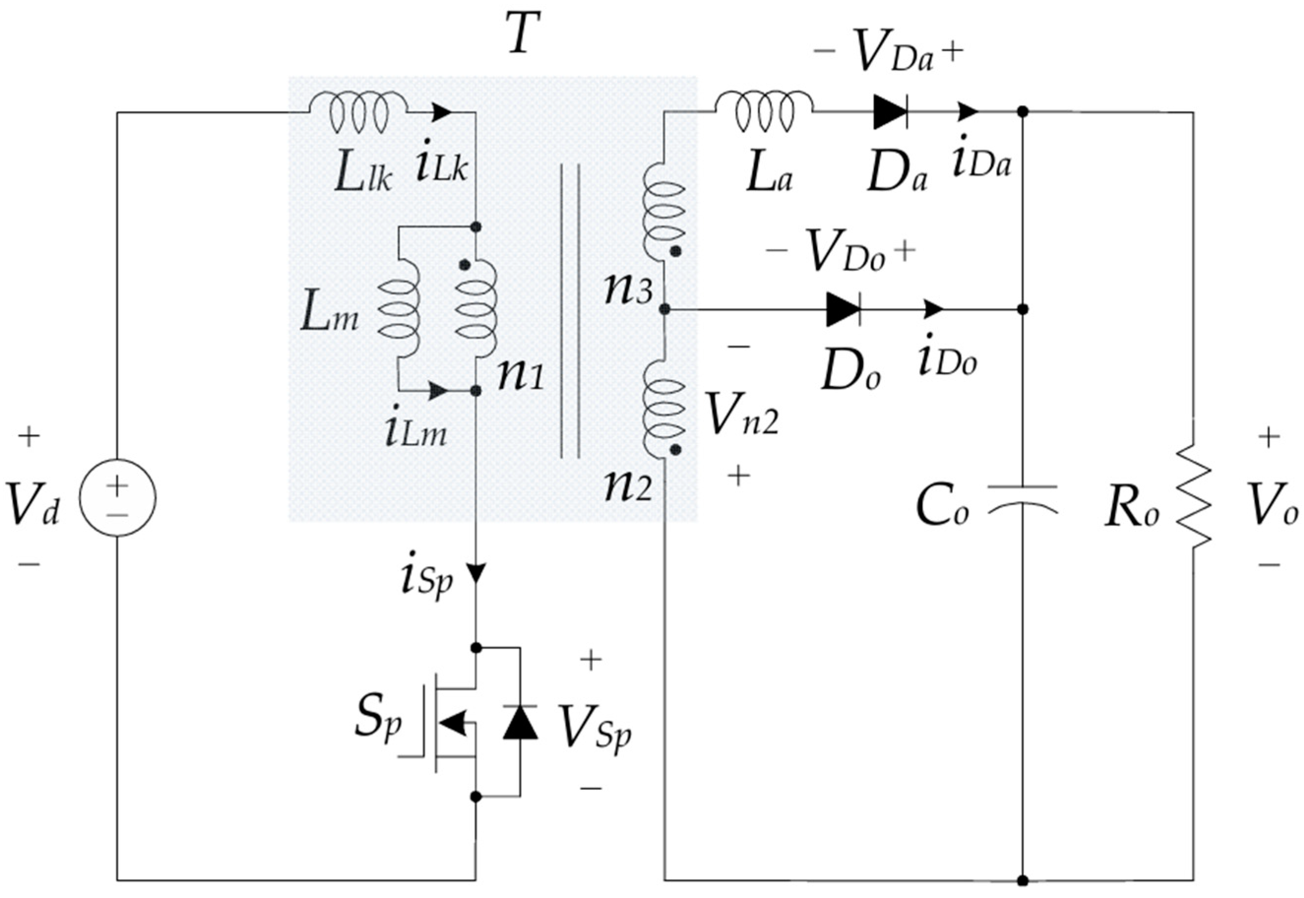
This paper proposes an effective method to improve the power efficiency of the flyback converter in the CCM. The proposed flyback converter includes a simple passive circuit to reduce the switching power losses. Figure 2 shows the circuit diagram of the proposed flyback converter. The additional circuit includes one diode, one inductor, and one auxiliary winding of the transformer. The output diode current can be shifted to the new branch in the additional circuit. The output diode can be turned off at zero current, which eliminates the turn-off switching loss of the diode. The additional inductor is used to control the changing rate of the additional diode current to reduce the reverse-recovery current. Instead of using the soft-switching operations using the LC resonance, the proposed method utilizes the current shifting operation of the diode currents. It is advantageous for mitigating the saturation of the magnetic core to extend its operation range [21]. It is also beneficial for thermal management and the reduction of electromagnetic interference [22]. Keeping the advantageous simplicity of the passive method, the proposed converter reduces the switching power losses, improving the power efficiency.
The circuit configuration and the operation principle of the proposed converter are described in Section 2. The design considerations for the circuit components are presented along with the simulation verification in Section 3. The experimental results are given to evaluate the performance of the proposed converter in Section 4. The future research directions for the applications of the proposed converter are discussed in Section 5. Finally, Section 6 presents the concluding remark of the paper. With the motivation to improve the power efficiency of the flyback converter, the main contributions of this paper are to suggest an effective scheme to reduce the switching power losses by using a simple passive circuit, to present its operation principle, to evaluate experimentally its performance, and to discuss its applications. Considering the application of the flyback converter, the single-stage power factor correction [23,24,25,26] is one of the attractive applications. By integrating two power conversion stages into one, the single-stage flyback converters reduce the component count and correct the power factor [23]. A single-stage, single-switch converter method has been proposed by integrating the boost converter switching cell with the conventional flyback converter in [24]. On the other hand, asymmetrical pulse-width modulation (APWM) has been applied to the flyback converter for the single-stage power factor correction in [25]. The soft-switching operation, such as the zero-voltage switching, is achieved by an additional power switch on the primary side. A boost inductor is included for the DCM boost rectifier operation. However, the use of the additional active switch increases the manufacturing cost, losing the benefits of the flyback converter. In [26], a new method using a dual-purpose inverter has been proposed for the single-stage converter applications of the flyback converter. A low-power dual-purpose inverter has been included for the active harmonic compensation and for the output voltage regulation, respectively. However, the converter in [26] not only uses the BCM operation but also requires the additional power stage for implementing the dual-purpose inverter. In Section 5, the features of the proposed converter are compared to the features of the previous converters in [25,26] for the single-phase power factor corrections. Considering the advantages of the simple circuit structure and the improved power efficiency, the proposed converter is expected to be a cost-effective single-stage, single-switch converter.

2. Proposed Converter

2.1. Circuit Configuration

The proposed converter has two parts, as shown in Figure 2. The first part is the flyback converter, which consists of Sp, T, Do, and Co. The switch Sp operates with a constant switching frequency fs. It has an intrinsic body diode in parallel. The transformer T is modeled as an ideal transformer with the magnetizing inductor Lm and the leakage inductor Llk on the primary side. Lm is large enough so that the flyback converter operates in the CCM. T has the turns ratio of n1:n2:n3. n1 is the number of the primary winding turns connected to Sp. n2 is the number of the secondary winding turns connected to the output diode Do. The output capacitor Co is large enough so that the output voltage Vo is constant with respect to the input voltage Vd. The second part is the additional circuit, which consists of Da, La, and n3. n3 is the number of the auxiliary winding turns connected to La directly. The additional inductor La helps reduce the reverse-recovery current of the additional diode Da.

2.2. Operation Principle

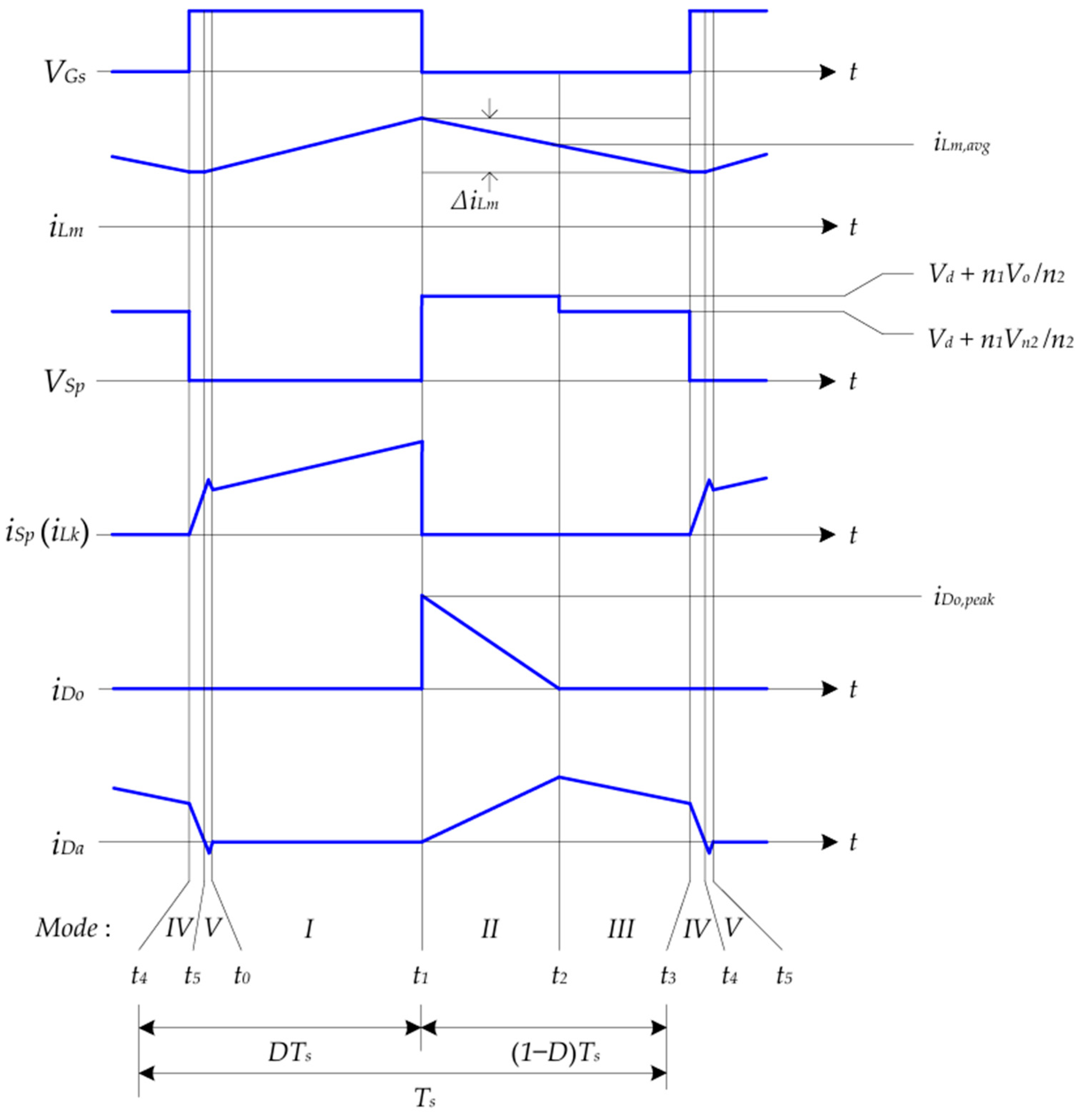
Figure 3 shows the operation modes of the proposed converter. Figure 4 shows the operation waveforms of the proposed converter. D is the duty ratio of the switch Sp. The proposed converter has five operation modes during one switching period Ts (=1/fs) as follows:
Mode I: At t = to, the switch Sp has been turned on. As the input voltage Vd has been applied to Lm and Llk, the magnetizing current iLm increases linearly at the rate of
d i L m d t = V d L m + L l k   .
The diodes Do and Da have been turned off on the secondary side.
Mode II: At t = t1, the switch Sp is turned off. The energy stored in Lm is transferred to the secondary side, causing the current to flow through the diodes Do and Da. As the output diode Do is turned on, the voltage across the winding n2 is Vo. As n3Vo/n2 is applied to the winding n3, the additional diode current iDa increases linearly at the rate of
d i D a d t = V o L a n 3 n 2 .  
As −n1Vo/n2 is applied to Lm, the magnetizing current iLm decreases linearly. By reflecting the magnetizing current iLm to the secondary side, the decreasing rate of the output diode current iDo can be represented as
d i D o d t = V o L m n 1 n 2 2 V o L a n 3 n 2 .
Due to the simultaneous turn-on of the diodes Do and Da, the output diode current iDo is shifted to the additional circuit branch. The output diode current iDo becomes zero at the end of Mode II. The time duration in Mode II can be represented as
t 12 = t 2 t 1 = i D o , p e a k V o 1 L m n 1 n 2 2 + 1 L a n 3 n 2
where iDo,peak is the peak current of the output diode Do. This mode ends when the output diode current iDo becomes zero. At the beginning of this mode, the energy stored in Llk should be released as the switch Sp is turned off. Along with the stray capacitances for the switch and the transformer, the leakage inductor causes a parasitic oscillation. This parasitic oscillation exists for some time at the beginning of this mode.
Mode III: At t = t2, the output diode Do is turned off at zero current. The zero-current switching of the output diode Do is achieved, which eliminates the turn-off switching loss. As the additional diode Da is still in the conduction state, the current flows through n2, n3, La, Do, and Co. By reflecting the magnetizing inductance Lm to the secondary side, the decreasing rate of the additional diode current iDa can be represented as
d i D a d t = V o L m n 2   + n 3 n 1 2 + L a .  
As the output voltage Vo is applied to n2, n3, and La, the voltage Vn2 across n2 can be represented as
V n 2 = L m V o n 2 n 1 2 L m n 2 n 1 2 + L m n 3 n 1 2 + L a = V o 1 + n 3 n 2 2 + L a L m n 1 n 2 2                   .  
The voltage across Lm becomes −n1Vn2/n2. As Vn2 is lower than Vo, the voltage VSp across the switch Sp can be reduced.
Mode IV: At t = t3, a turn-on gate signal VGs is applied to the gate of the switch Sp. As the input voltage Vd is applied to Lm and Llk, the following voltage equation can be obtained at the secondary side as
n 2 + n 3 n 1 L m L m + L l k V d + L a d i D a d t + V o = 0 .
From (7), the decreasing rate of the additional diode current iDa is represented as
d i D a d t = V o + n 2 + n 3 n 1 L m L m + L l k V d L a .
The decreasing rate of the additional diode current iDa is controlled by the additional inductor La, which can alleviate the reverse-recovery process of the additional diode Da.
Mode V: At t = t4, the additional diode current iDa becomes zero. However, the additional diode Da is not immediately turned off because the reverse-recovery process makes the diode conduct reversely to discharge its reverse-recovery charge. As the switch Sp is been turned on, the reverse-recovery current of the additional diode Da is reflected to the primary side through the transformer T. As the diode reverse-recovery current is reduced, the turn-on switching loss for the switch Sp can be reduced as well. At the end of Mode V, the stored charge is recovered from the junction of the additional diode Da.

3. Design Considerations

3.1. Voltage Gain and Magnetizing Inductance

By the volt-second balance for the transformer T, the following relation can be written as
L m L m + L l k V d D T s = V o n 1 n 2 t 12                                                                         + V o 1 + n 3 n 2 2 + L a L m n 1 n 2 2 n 1 n 2 1 D T s t 12   .
By rearranging (9), the following voltage relation can be obtained for the voltage gain of the proposed converter as
V o V d = n 2 n 1 D T s 1 + L l k L m 1 1 D T s + 1 α 1 t 12 1 α
where
α = 1 1 + n 3 n 2 2 + L a L m n 1 n 2 2   .
Supposed that α is one and Llk is zero, the voltage gain in (10) can be considered as the voltage relation of the conventional flyback converter in the CCM, which is
V o V d = n 2 n 1 D 1 D .
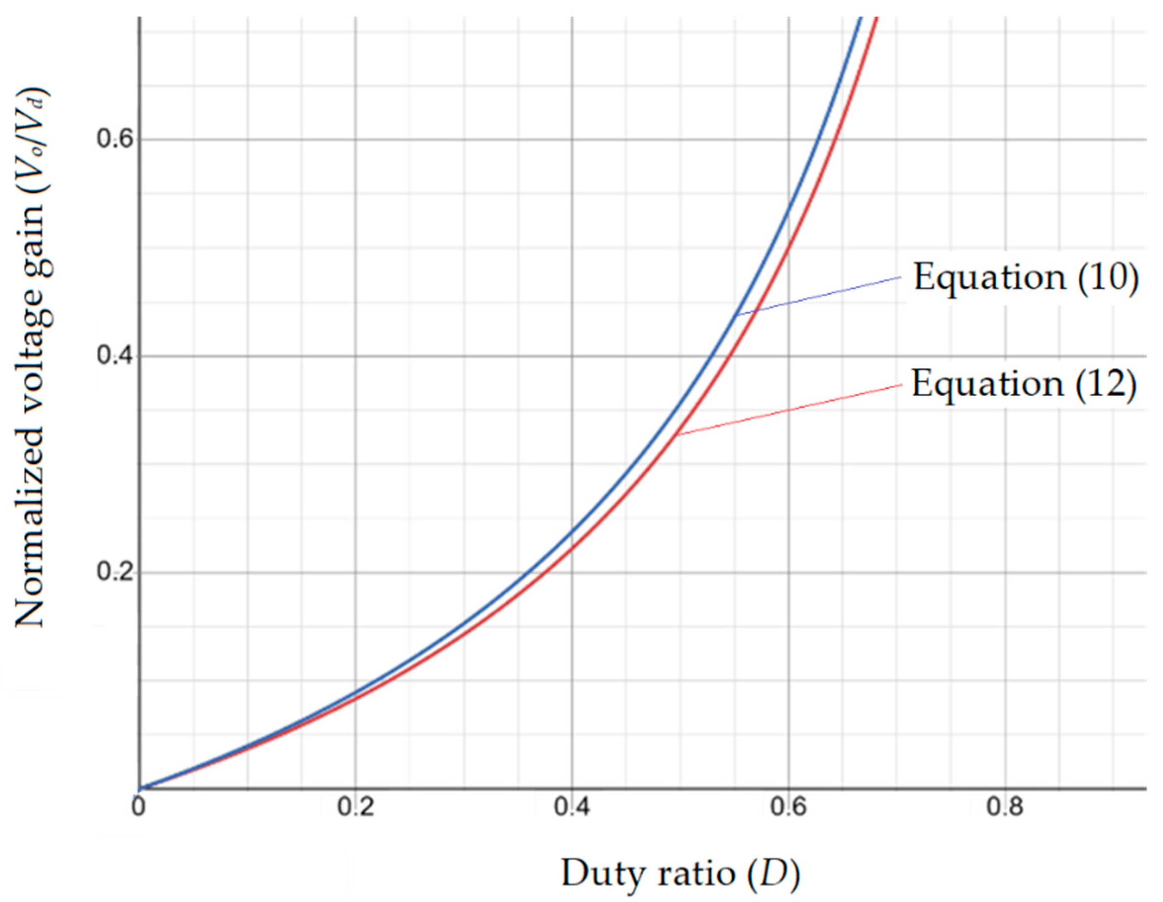
Figure 5 shows the normalized voltage gain curves. The curve in red is obtained from (12) with the parameters for Vo = 15 V, Vd = 48 V, n1 = 30, and n2 = 10. The duty ratio D = 0.48 is obtained for the normalized voltage gain of Vo/Vd = 0.31. On the other hand, the curve in blue is obtained from (10) with the parameters for Vo = 15 V, Vd = 48 V, fs = 50 kHz, Lm = 300 μH, Llk = 1 μH, La = 7 μH, n1 = 30, n2 = 10, and n3 = 2. The duty ratio D = 0.46 is obtained for the normalized voltage gain of Vo/Vd = 0.31. As shown in Figure 5, the voltage gain in (10) with the parameters mentioned above is higher than the voltage gain in (12) with respect to the duty ratio D. The voltage gain of the proposed converter is more effective as the duty ratio can be reduced for obtaining the same normalized voltage gain compared to the conventional converter. Once the duty ratio D is decided for Vd and Vo, n1 and n2 can be decided in advance by considering (12). Since the proposed converter operates in the CCM, the magnetizing inductor could be chosen as
L m > 2 P o i S p 2 f s  
where Po is the output power, and iSp is the switch current which is the same as the leakage inductor current iLk. For the design of high-frequency transformers, the gapped ferrite cores can be used for avoiding the saturation. By adding an air gap to the solid ferrite core, the number of ampere-turns can be increased so that the ferrite core can tolerate before it saturates.

3.2. Auxiliary Winding Turns and Additional Inductor

When the power switch Sp is turned off, the output diode current iDo is shifted to the additional circuit branch. The output diode Do can be turned off at zero current. As shown in Figure 4, for the zero-current switching of the output diode Do, the time duration in Mode II should be less than the turn-off time of the switch Sp as
t 12 < 1 D T s .  
By applying (4) to (14), the following equation can be represented as
V o 1 L m n 1 n 2 2 + 1 L a n 3 n 2 > i D o , p e a k 1 D T s   .  
Here, the peak output diode current iDo,peak is expressed as
i D o , p e a k = i D o , a v g + 0.5 Δ i D o
where iDo,avg and ΔiDo are the average current and the ripple current of the output diode Do, respectively, during one switching period Ts. Because the secondary current is related to the primary current through the inverse turns-ratio of the transformer [28], the peak output diode current iDo,peak can be represented as
i D o , p e a k = i L m , a v g n 1 n 2 + 0.5 Δ i L m n 1 n 2
where iLm,avg and ΔiLm are the average current and the ripple current of the magnetizing current iLm, respectively, during one switching period Ts. Assuming that the converter is lossless, (17) can be expressed as
i D o , p e a k = P o V d n 1 n 2 + 1 D V o T s 2 L m n 1 n 2 2 .  
By applying (18) to (15), the following condition for selecting n3 can be obtained as
n 3 > n 1 L a I o V d f s 1 D 1 2 L m n 1 n 2
where Io is the output current. While the auxiliary winding turns satisfied with (19), the time duration in Mode II is ensured for the current shifting operation of the proposed converter. The inductance of the additional inductor can be selected based on (8) as
L a > V o + n 2 + n 3 n 1 L m L m + L l k V d d i D a d t .  
The changing rate of the additional diode current iDa is controlled by the additional inductor La. As La gets higher, the changing rate of the additional diode current iDa is reduced, which decreases the reverse-recovery current of Da. For the design of high-frequency inductors, a commonly simple scheme called the area-product method [29] can be adopted where the thermal considerations are ignored. It implies that the high-frequency inductor built on this design should be evaluated for its temperature rise and efficiency. Of course, the core size should be adjusted accordingly. Figure 6 shows the operation waveforms of the proposed converter for the exceptional design case. When the inductance for the additional inductor La is very large, the output diode current iDo will not be zero before the power switch is turned on. Because the increasing rate of the additional diode current iDa is so low, the output diode current iDo is not turned off at zero current. Despite the use of the transformer auxiliary winding turns, the output diode cannot achieve the zero-current switching operation. The output diode and the additional diode will have their reverse-recovery processes for Mode IV and Mode V, respectively, as shown in Figure 6. Therefore, the inductance of the additional inductor should be chosen experimentally, considering the exceptional operation modes in Figure 6.

3.3. Output Capacitor and Switching Devices

The capacitance of the output capacitor can be chosen based on the output voltage ripple ΔVo as
C o > I o D f s V o .
As the capacitance of the output capacitor is higher, the ripple of the output voltage is reduced. For the selection of the switching devices, the reverse blocking voltage should be considered with the parasitic oscillations. For the power switch Sp, its reverse blocking voltage is Vd + n1Vo/n2 theoretically. For the additional diode Da, its reverse blocking voltage is theoretically Vo + n2Vd/n1 + n2Vd/n1. However, considering the energy stored in the leakage inductor and the reverse-recovery process of the additional diode, the voltage rating for Sp and Da, respectively, should be at least two times higher than the reverse blocking voltage of each device. On the other hand, theoretically, for the output diode Do, the reverse blocking voltage is Vo + n2Vd/n1. As the output Do is turned off at zero current, additional voltage stress is not imposed on the diode, which permits the use of a lower voltage rating device for Do. For the selection of the diodes, the forward voltage drop is a major concern. In applications with low output voltages, the Schottky diode can be used with a low voltage drop. Being majority-carrier devices, the Schottky diodes switch fast and keep switching losses to a minimum compared to the fast-recovery diodes.

3.4. Simulation Verification

The simulation results have been obtained for the conventional converter and the proposed converter, respectively. The simulations have been carried out by the physical security information management (PSIM) software, the version of which is 2023.a. The integration time step for the simulation has been set as 10 ns. By deliberating the design considerations described above, the key simulation parameters have been obtained as Vd = 48 V, Vo = 15 V, Po = 45 W, fs = 50 kHz, Lm = 300 μH, Llk = 1 μH, n1 = 30, n2 = 10, and Co = 2200 μF.
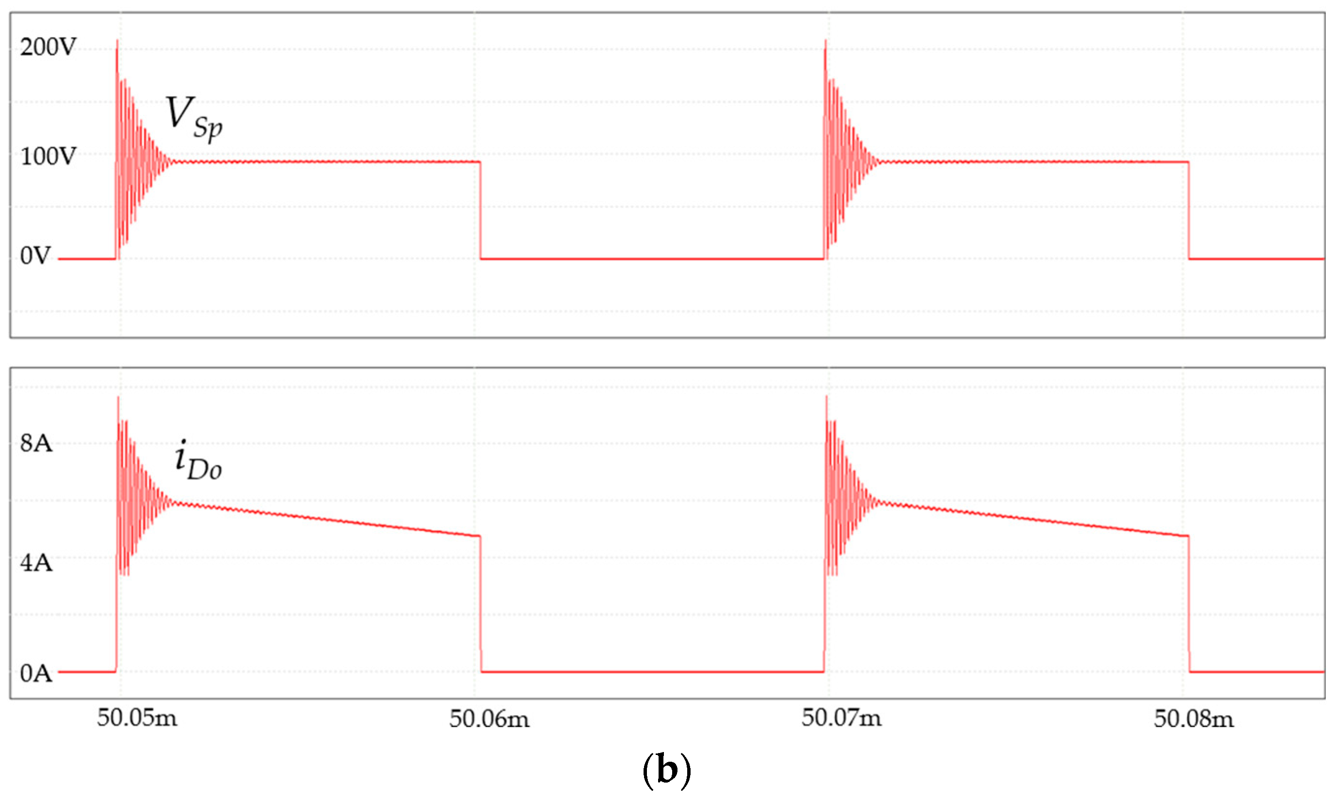
Figure 7 shows the simulation results of the conventional converter. Figure 7a shows VSp and iSp. The switch current iSp increases for the turn-on period of the switch Sp. Figure 7b shows VSp and iDo. The output current iDo decreases for the turn-off period of the switch Sp. When the switch Sp is turned off, a parasitic oscillation is observed across Sp. Because the energy stored in the leakage inductor Llk should be released, a parasitic oscillation has been observed. There is a parasitic oscillation between the leakage inductor and the stray capacitors in the converter. These stray capacitors include the parasitic capacitor CSp of the switch and the parasitic capacitor CTr of the transformer. In the simulations, CSp and CTr are chosen as CSp = 200 pF and CTr = 100 pF, respectively. The parasitic oscillation affects the voltage and current waveforms of the circuit components.
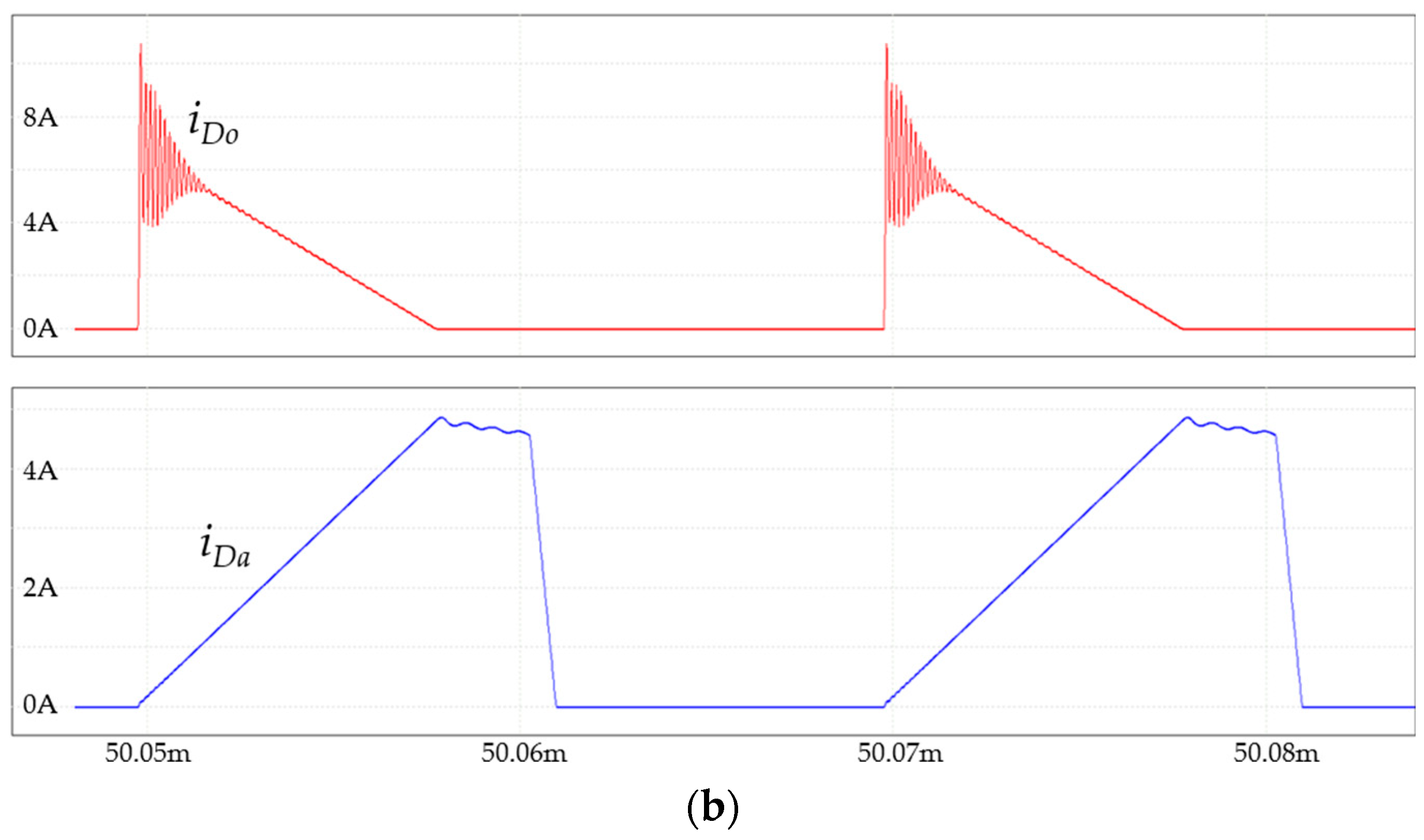
Figure 8 shows the simulation results of the proposed converter. The additional parameters for La = 7 μH and n3 = 2 have been included in the simulation. Figure 8a shows VSp and iSp. The switch current iSp increases for the turn-on period of the switch Sp. The switch voltage VSp has been reduced during the turn-off period by the operation of the additional circuit. When the switch Sp is turned off, a parasitic oscillation is observed across Sp because the energy stored in Llk is released along with the stray capacitors in the converter. Figure 8b shows iDo and iDa. The current iDo through the output diode Do is shifted to the additional diode Da. When the output diode current iDo is reduced to zero, the additional diode current iDa changes its direction. The output diode Do is turned off at zero current, while the additional diode Da is turned on at zero current.

4. Experimental Results

4.1. Experimental Setup

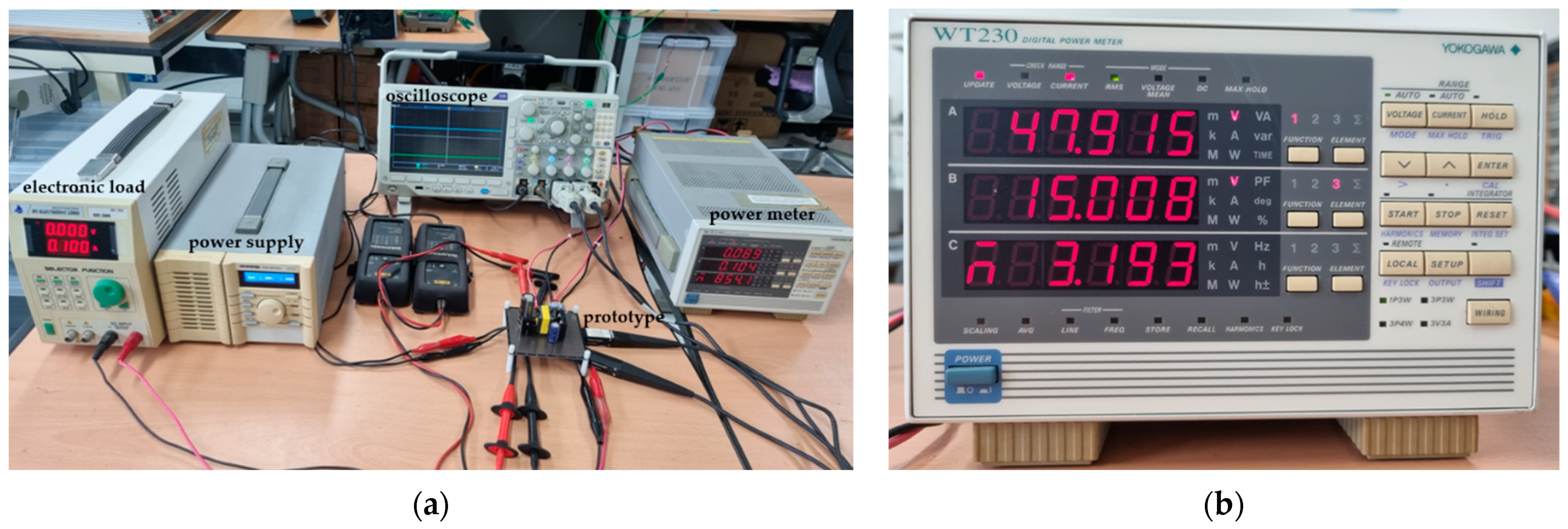
A 45 W prototype converter has been built and tested to evaluate the performance of the proposed converter. The conventional converter has also been designed to compare its performance with the proposed converter. Figure 9 shows the pictures for the experimental setup. Figure 9a shows the picture of the test environment, including the measurement instruments, the power supply, and the prototype circuit.
The programmable power supply PSH-6012A (GW-INSTEK, Seoul, Republic of Korea) has been used to supply the dc input voltage. The programmable electronic load ESL-300 (PNCYS, Seoul, Republic of Korea) has been used for the dc output load. The oscilloscope MDO3014 (Tektronix, Beaverton, OR, USA) has been used along with the voltage probes P5200 (Tektronix, USA) and the current probes TCP202 (Tektronix, USA). The digital power meter WT-230 (YOKOGAWA, Tokyo, Japan) has been utilized to measure power efficiency. The power efficiency has been obtained by dividing the output power by the input power. As shown in Figure 9b, the digital power meter measures the parameters up to 3 decimal places so that the power efficiency measurement can be as accurate as possible.
Table 1 shows the electrical specifications and the circuit parameters. The transformer T has been designed by using an EFD2525S PQ core (Samwha Electronics, Yongin, Republic of Korea) with a 0.3 mm air gap. The inductor La has been designed by using an OR16 toroidal core (Samwha Electronics, Republic of Korea) with 5 winding turns. The magnetic components and the switching devices have been selected based on the design considerations discussed in the previous section.
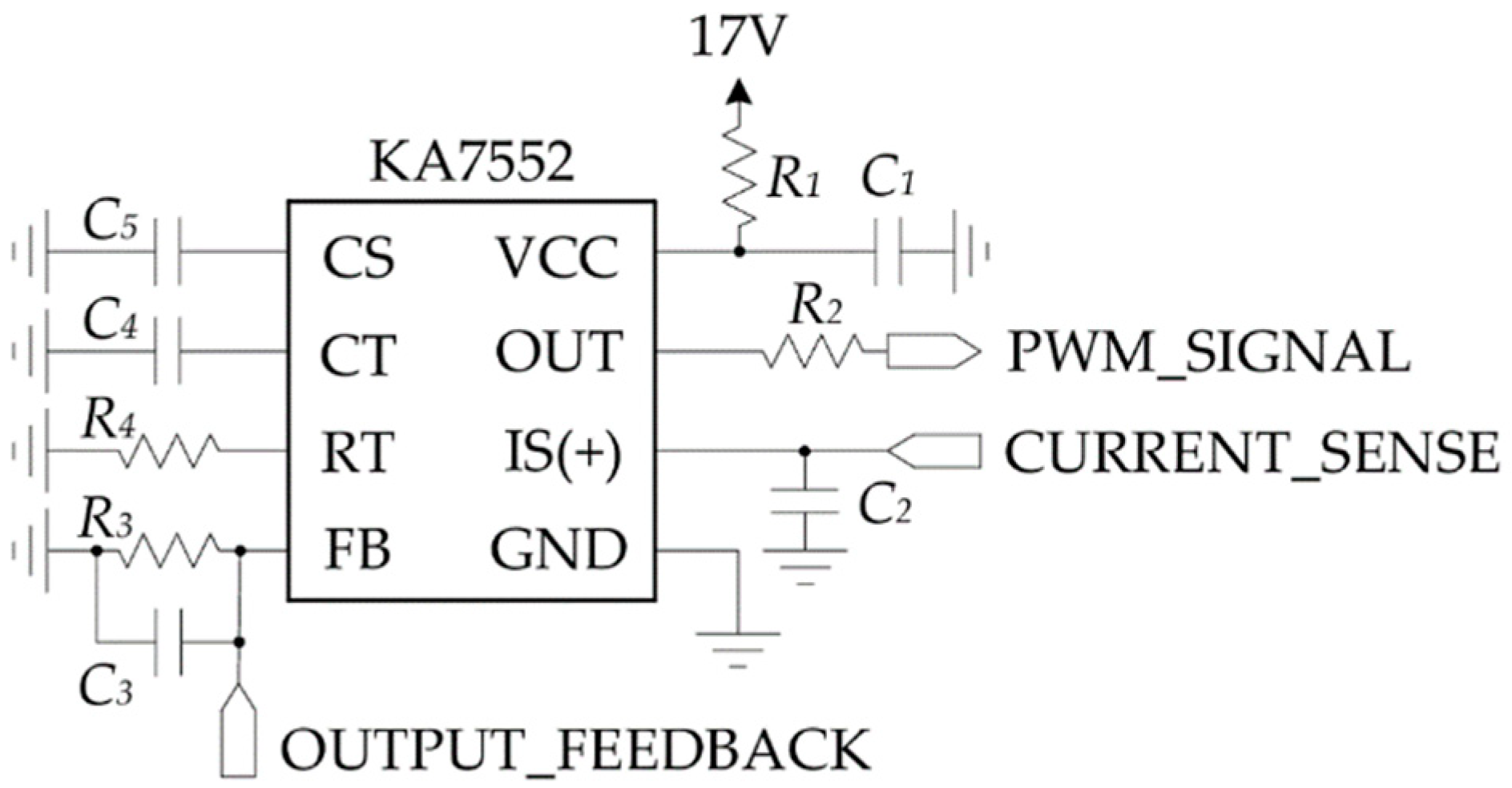
The control circuit has been implemented using the pulse-width modulation controller KA7552 (On Semiconductor, Phoenix, AZ, USA) to regulate the output voltage. Figure 10 shows the circuit diagram for the control circuit implementation. To implement the closed-loop control of the converter, the following components have been used as R1 = 10 Ω, R2 = 100 Ω R3 = 10 kΩ, R4 = 5.3 kΩ, C1 = 1 μF, C2 = 1 nF, C3 = 1 nF, C4 = 3.3 nF, and C5 = 470 nF. There are three signals interfaced with the power stages of the proposed converter. In Figure 10, the first signal is PWM_SIGNAL, which is connected to the gate of the power switch Sp. The second signal is CURRENT_SENSE, which senses the voltage across the resistor between the source of the power switch Sp and the electrical ground. The third signal is OUTPUT_FEEDBACK, which comes from the output voltage feedback circuitry. For the negative feedback control with galvanic isolation, the photocoupler PC817 and the shunt regulator TL431 have been utilized.

4.2. Experimental Verifications

Figure 11 shows the experimental waveforms of the conventional converter. Figure 11a shows VSp and iSp. As discussed in the simulation results, the voltage and current oscillations are observed due to the parasitic components in the circuit. Figure 11b shows VSp and iSp for the enlarged Figure 11a. It is observed that the switching loss is significant for the turn-on process of the switch Sp.
Figure 12 shows the experimental waveforms of the proposed converter. Figure 12a shows VSp and iSp. Figure 12b shows VSp and iSp for the enlarged Figure 12a. It is shown that the switch voltage VSp has been reduced during the turn-off of the switch Sp. It is also observed that the changing rate of the switch current iSp has been reduced for the turn-on process, compared to iSp in Figure 11b. As shown in Figure 12b, the turn-on switching loss has been reduced for the switch Sp.
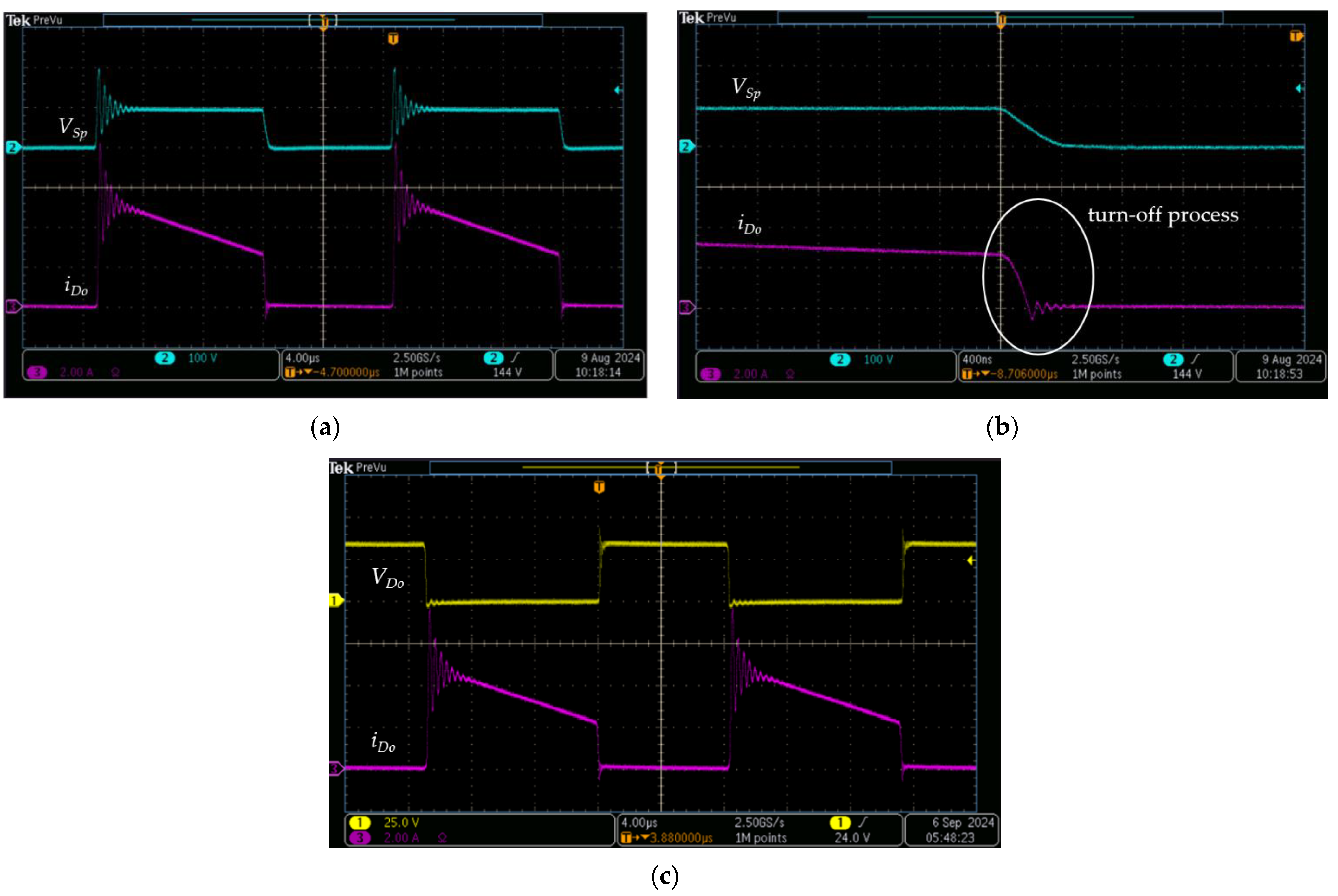
Figure 13 shows the experimental waveforms of the conventional converter. Figure 13a shows VSp and iDo. Figure 13b shows VSp and iDo for the enlarged Figure 13a. It is observed that the reverse-recovery process is significant for the output diode Do in its turn-off process. The reverse-recovery time is approximately 350 ns, considering the parasitic oscillation time. Figure 13c shows VDo and iDo where the blocking voltage of the output diode is observed.
Figure 14 shows the experimental waveforms of the proposed converter. Figure 14a shows iDo and iDa. Figure 14b shows VSp and iDa. As shown in Figure 14a,b, the output diode current iDo is shifted to the additional diode Da by the operation of the additional circuit. The additional diode Da is turned on at zero current. As the output diode current iDo is reduced to zero, the additional diode current iDa changes its direction. The output diode Do is turned off at zero current. Figure 14c shows VSp and iDa for the enlarged Figure 14b. It is observed that the reverse-recovery process has been reduced for the additional diode Da for the turn-off process. The reverse-recovery time is approximately 200 ns, considering the parasitic oscillation period. It is shown that the diode reverse-recovery current has been reduced by lowering the decreasing rate of the additional diode Da during its turn-off instant. Figure 14d shows VDo and iDo. Figure 14e shows VDa and iDa. The blocking voltages for the diodes Do and Da are observed in Figure 14d,e, respectively. Figure 14f shows Vo and Io. As shown in Figure 14f, the output voltage Vo is regulated well when the output load Io changes abruptly from 1.0 A to 0.5 A.
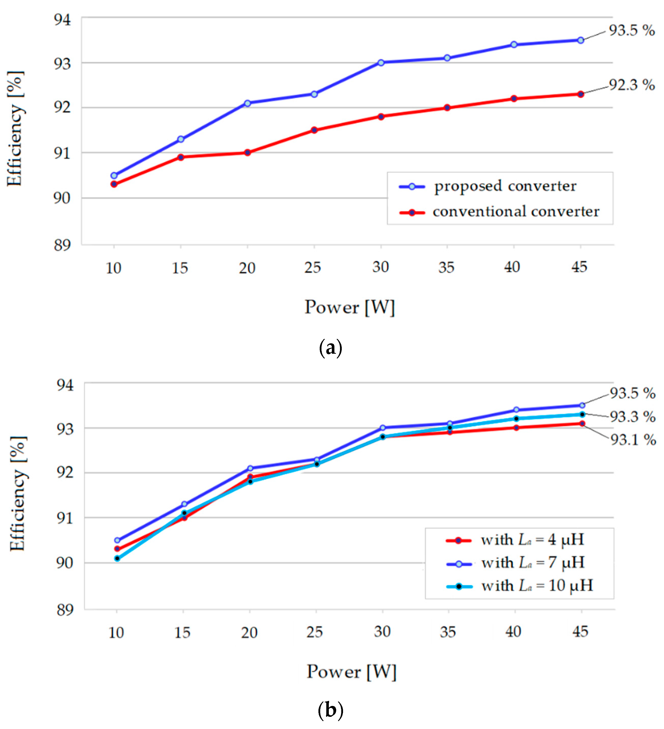
Figure 15 shows the measured power efficiency curves. To consider the uncertainty of the measurement of the power efficiency, the upper limit and the lower limit for the measured power efficiency are 0.05% and—0.05%, respectively. For an example of the measurement result of 91.5 ± 0.05%, the measured power efficiency ranges between 91.45% and 91.55%. With the tolerance limit range from 0.05% to 0.05%, the difference between the measured power efficiencies has been calculated for the experimental results. Figure 15a shows the power efficiency curves for the conventional converter and the proposed converter with La = 7 μH, respectively, for different output power levels. As shown in Figure 15a, the conventional converter has a power efficiency of 92.3% at the rated load condition. On the other hand, the proposed converter has a power efficiency of 93.5% at the rated load condition. It has improved the power efficiency by 1.2% compared to the conventional converter. Figure 15b shows the power efficiency curves of the proposed converter for different inductances of La. The proposed converter has achieved the highest power efficiency of 93.5% for La = 7 μH for the rated load condition. In the case of using low inductance, the proposed converter has obtained the power efficiency of 93.1% for La = 4 μH. On the other hand, the proposed converter has obtained a power efficiency of 93.3% for La = 10 μH in the case of using high inductance.
Figure 16 shows the power loss distributions for the proposed converter with respect to the experimental results in Figure 15a. The power losses have been calculated based on the theoretical power loss model [30]. Sp, Da, and Do have caused the switching losses, which account for 42% of the total losses. The conduction losses for Sp, Da, and Do account for 29% of the total losses. The magnetic losses for T and La account for 17% of the total losses. Other losses include the power losses associated with the capacitor and the control circuitry. The highest losses are the switching losses, which can be reduced by achieving the soft-switching operation of the power switch on the primary side. Another approach to improve power efficiency is to use the synchronous rectifier [31], which can reduce conduction losses by replacing the diode with the power switch.
Table 2 compares the electrical specifications and the power efficiency of the previous converters. Table 3 compares the components required for the passive snubber methods in [18,19,20] and the proposed converter.
Figure 17 shows the measured power efficiency curves to evaluate the performance of the proposed converter. The previous converter in [18] has been designed and tested under the same electrical specifications as the proposed converter. The additional components for the inductor, diode, capacitor, and coupled inductor have been included in applying the lossless snubber circuit in [18] to the flyback converter. Figure 17a shows measured power efficiency curves for the proposed converter and the converter in [18], respectively. The proposed converter has achieved higher power efficiency than the converter in [18], as shown in Figure 17a. The converter using the lossless snubber method in [18] achieves the soft-switching operation for the switch and the diode, respectively. However, the conduction losses are increased because a lot of the diodes are utilized. In addition, the high current stresses on the magnetic components increase the magnetic losses. Considering the components and the circuit complexity shown in Table 3, the proposed converter provides a low cost and higher power efficiency compared to the previous converters. To evaluate the proposed converter for higher power levels, a 90 W prototype converter has been designed and tested under the same input and output voltage specification in Table 1. Figure 17b shows the measured power efficiency curve of the proposed converter tested for the 90 W rated load condition. Because the output current has been doubled, the current ratings of the switch devices have been enhanced as Sp = IRFB4137PbF and Da = Do = MBR20100CT. The transformer T has been designed by using an EFD3130S PQ core (Samwha Electronics, Republic of Korea) with n1:n2: n3 = 30:10:3. The parallel winding has been utilized for reducing the wire conduction losses of the transformer. As shown in Figure 17b, the proposed converter has achieved an efficiency of 93.6% at the 70 W load condition and 93.3% at the 90 W rated load condition, respectively.

5. Discussion

5.1. Application for Auxiliary Power Supplies

In this study, the proposed converter has been designed and tested for the use of the auxiliary power supply in low-voltage electric motor drive systems [4]. Typical examples are 48 V automotive systems like low-speed electric vehicles [32]. These kinds of applications need a highly efficient and highly reliable auxiliary power supply to provide a constant output voltage with electrical isolation. Furthermore, manufacturing costs are one of the key design issues for commercial products. Considering the high input voltage applications [12,13], the soft-switching techniques to recycle the transformer leakage energy would be desirable to improve the power efficiency. However, the soft-switching methods will increase the cost when the flyback converter is applied for low input voltage applications despite its advantages. Therefore, the proposed converter provides a simple and effective method to improve power efficiency by reducing the power losses of the switching devices, which will be desirable for the cost-effective design of the flyback converter.

5.2. Application for Power Factor Corrections

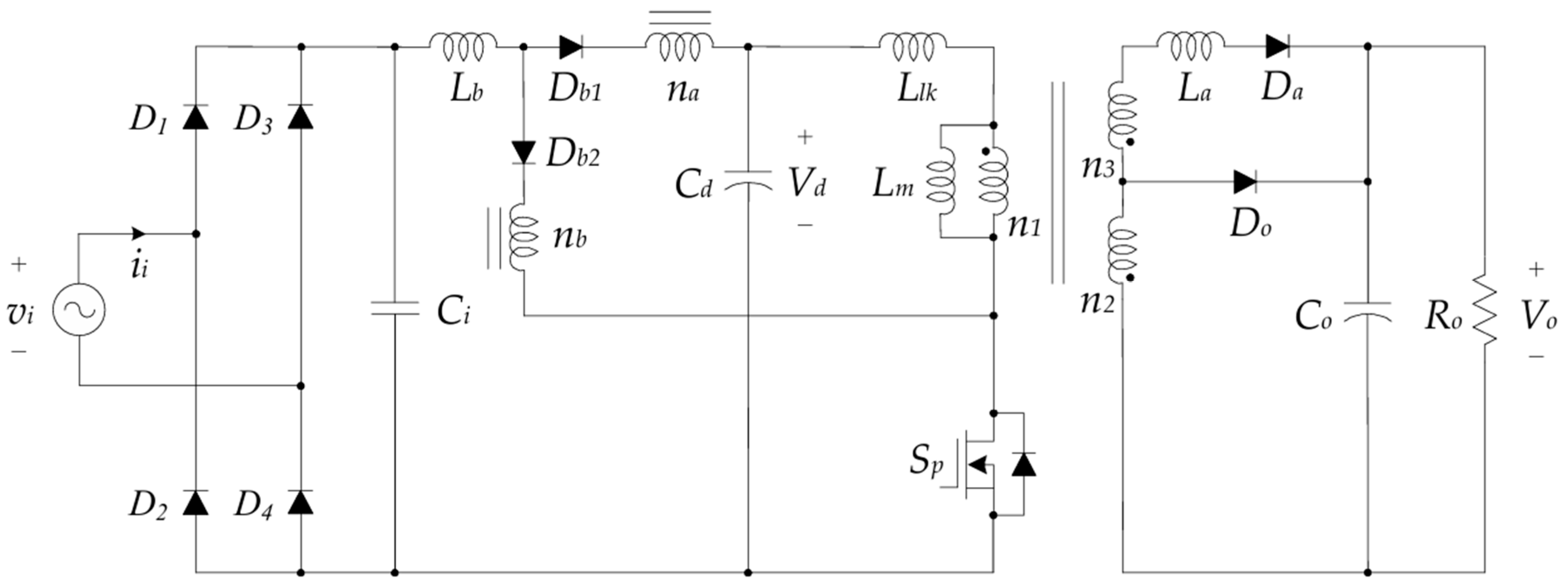
Single-stage power factor correction techniques have been actively researched using the flyback converter [23,24,25,26]. By integrating two power conversion stages into one, the single-stage ac–dc converters reduce the component count and the manufacturing cost [23]. As described in [24], as a single-switch converter, the flyback converter can be utilized for the cost-effective single-stage ac–dc converters. The proposed converter is expected to be a good candidate for single-stage power factor correction applications because it uses only one power switch. Figure 18 shows the circuit diagram of the proposed converter applied for the single-stage, single-switch power factor correction. In Figure 18, the power factor correction circuit components, including Ci, Lb, Db1, Db2, na, and nb, are added to the proposed flyback converter. vi is the single-phase grid voltage. The single-phase full-bridge diode rectifier includes D1, D2, D3, and D4. One coupled inductor can be utilized to realize the coupled windings for na and nb. Cd is the dc-link capacitor, which is the dc input voltage for the proposed flyback converter. By the pulse-width modulation for the power switch Sp, the output voltage Vo is regulated, while the input current ii is controlled to improve the power factor. For the proposed converter in Figure 18, the operation principle of the converter, the optimal design of the magnetic components, the analysis of the power factor, and the dc-link voltage regulation scheme will be further research topics. Table 4 compares the features of the proposed flyback converter with the features of the previous converters in [25,26] for the single-stage power factor corrections.
The flyback converter in [25] operates with the APWM. Two power switches are required for the half-bridge switching leg to realize the zero-voltage switching operation of the power switches. The flyback converter in [26] needs a dual-purpose inverter for the active harmonic compensation and for the output voltage regulation. Totally, five power switches are required for implementing both the flyback converter and the dual-purpose inverter. The BCM operation is adopted to control the flyback converter, while an extra dual-mode control is applied to the dual-purpose inverter. Compared to the previous converter in [25,26], the proposed converter in Figure 18 is expected to reduce the circuit complexity and improve the power efficiency for a single-stage, single-switch converter.

6. Concluding Remark

This paper has proposed a flyback converter with a simple passive circuit to improve power efficiency. The additional passive circuit includes one diode, one inductor, and one auxiliary winding of the transformer. The current through the output diode has been shifted to the new branch in the additional circuit. The output diode has been turned off at zero current, which eliminates the turn-off switching loss. The additional diode has been turned on at zero current. The additional inductor has been utilized to control the changing rate of the additional diode current to reduce the reverse-recovery current. Therefore, the turn-on switching loss for the power switch has been reduced. Keeping the advantageous simplicity of the passive method, the proposed converter has reduced the switching power losses, improving the power efficiency.
The circuit configuration and the operation principle have been described. The design considerations for the circuit components and the simulation verification have been presented. The applications of the proposed converter have been discussed for future research directions. Experimental results for a 45 W prototype have been discussed to evaluate its performance. The proposed converter has achieved a power efficiency of 93.5% for the rated load condition, improving the power efficiency compared to the previous converters. Over the drawbacks of the previous converters, the proposed converter has reduced switching power losses with a simple and effective passive circuit method.

Funding

This research was supported by National University Development Project at Jeonbuk National University in 2023.

Data Availability Statement

The original contributions presented in the study are included in the article, further inquiries can be directed to the corresponding author.

Conflicts of Interest

The author declares no conflicts of interest.

References

  1. Zhu, B.; Yang, Y.; Wang, K.; Liu, J.; Vilathgamuwa, D.M. High transformer utilization ratio and high voltage conversion gain flyback converter for photovoltaic application. IEEE Trans. Ind. Appl. 2024, 60, 2840–2851. [Google Scholar] [CrossRef]
  2. Omer, S.A.; Abdulsamed, L.; Meltem, L.; Arda, A.; Bati, E.E.; Mehmet, O.G. Meta-heuristics based design and optimization of active clamp flyback converter for USB PD. IEEE Access 2024, 12, 29269–29280. [Google Scholar]
  3. Mario, P.S.; Daniel, S.P.; Oscar, M.R.B.; Luis, G.V.V.; Abraham, C.S.; Susana, E.D.L.A.; Claudia, C.G.; Yesica, I.S.B.; Ricardo, E.L.P.; Juan, A.A.T. Flyback converter for solid-state lighting applications with partial energy processing. Electronics 2021, 10, 60. [Google Scholar]
  4. Novakovic, B.; Stern, D.; Stamenkovic, I.; Milivojevic, N. Flyback converter as auxiliary power supply for low-cost single-phase motor system. In Proceedings of the International Conference on “Computer as a Tool” (EUROCON 2005), Belgrade, Serbia, 21–24 November 2005; pp. 1493–1496. [Google Scholar]
  5. Halder, T. A comparative study of the hard & soft switching of the flyback converters. In Proceedings of the 2014 IEEE Power India International Conference (PIICON), Delhi, India, 5–7 December 2014; pp. 1–5. [Google Scholar]
  6. Yuri, P.; Milan, M.J. Adaptive off-time control for variable-frequency, soft-switched flyback converter at light loads. IEEE Trans. Power Electron. 2002, 17, 596–603. [Google Scholar]
  7. Hong, J.P.; Moon, G.W. A digitally controlled soft valley change technique for a flyback converter. IEEE Trans. Ind. Electron. 2015, 62, 966–971. [Google Scholar] [CrossRef]
  8. Yoo, J.S.; Baek, J.O.; Ahn, T.Y. A high-efficiency QR flyback dc-dc converter with reduced switch voltage stress realized by applying a self-driven active snubber (SDAS). Energies 2023, 16, 1068. [Google Scholar] [CrossRef]
  9. Park, J.P.; Moon, Y.J.; Jeong, M.G.; Kang, J.G.; Kim, S.H.; Gong, J.C.; Yoo, C.S. Quasi-resonant controller with adaptive switching frequency reduction scheme for flyback converter. IEEE Trans. Ind. Electron. 2016, 63, 3571–3581. [Google Scholar] [CrossRef]
  10. Wang, C.; Xu, S.; Shen, W.; Lu, S.; Sun, W. A single-switched high-switching-frequency quasi-resonant flyback converter. IEEE Trans. Power Electron. 2019, 34, 8775–8786. [Google Scholar] [CrossRef]
  11. Sayeb, M.T.; Sayed, R.B.S.; Mohammad, R.T.H. A brief review of snubber circuits for flyback converter. In Proceedings of the 2018 International Conference for Convergence in Technology (I2CT), Pune, India, 6–7 April 2018; pp. 1–5. [Google Scholar]
  12. Watson, R.; Lee, F.C.; Hua, G.C. Utilization of an active-clamp circuit to achieve soft switching in flyback converters. IEEE Trans. Power Electron. 1996, 11, 162–169. [Google Scholar] [CrossRef]
  13. Tang, C.Y.; Lin, W.Z.; Tan, Y.C. An active clamp flyback converter with high precision primary-side regulation strategy. IEEE Trans. Power Electron. 2022, 37, 10281–10289. [Google Scholar] [CrossRef]
  14. Jacinto, M.J.M.; Esther, J.; Jose, V. Parasitic capacitance effects on active clamp flyback output characteristics: Application to IPOP connection. Energies 2022, 15, 3201. [Google Scholar] [CrossRef]
  15. Hadi, T.; Ebrahim, B.; Amirreza, Z.G. A full soft-switching ZVZCS flyback converter using an active auxiliary cell. IEEE Trans. Ind. Electron. 2017, 64, 1123–1129. [Google Scholar]
  16. Chung, H.H.; Hui, S.R.; Wang, W.H. A zero-current-switching PWM flyback converter with a simple auxiliary switch. IEEE Trans. Power Electron. 1999, 14, 329–342. [Google Scholar] [CrossRef]
  17. Li, J.; van Horck, F.B.; Daniel, B.J.; Bergveld, H.J. A high-switching-frequency flyback converter in resonant mode. IEEE Trans. Power Electron. 2017, 32, 8582–8592. [Google Scholar] [CrossRef]
  18. Mehdi, M.; Ehsan, A.; Mohammad, R.Y. Family of soft-switching single-switch PWM converters with lossless passive snubber. IEEE Trans. Ind. Electron. 2015, 62, 3473–3481. [Google Scholar]
  19. Mehdi, M.; Martin, O. Flyback lossless passive snubber. In Proceedings of the 2015 IEEE Energy Conversion Congress and Exposition (ECCE), Montreal, QC, Canada, 20–24 September 2015; pp. 5896–5901. [Google Scholar]
  20. Adel, A.; Gerry, M. A comparative study of two passive regenerative snubbers for flyback converters. In Proceedings of the 2018 IEEE International Symposium on Circuits and Systems (ISCAS), Florence, Italy, 27–30 May 2018; pp. 1–7. [Google Scholar]
  21. Gianpaolo, V.; Guiseppe, L.; Daniel, S. Thermal stability of a DC/DC converter with inductor in partial saturation. IEEE Trans. Ind. Electron. 2021, 68, 7985–7995. [Google Scholar]
  22. Daniele, S.; Giuseppe, L.; Gianpaolo, V. Assessment of the current for a non-linear power inductor including temperature in DC-DC converters. Electronics 2023, 12, 579. [Google Scholar] [CrossRef]
  23. Gerry, M.; Praveen, J. Single-phase single-stage power-factor-corrected converter topologies. IEEE Trans. Ind. Electron. 2005, 52, 23–35. [Google Scholar]
  24. Laszlo, H.; Milan, M.J. Single-stage single-switch input-current-shaping technique with reduced switching loss. IEEE Trans. Power Electron. 2000, 15, 681–687. [Google Scholar]
  25. Giorgio, S.; Simone, B. An isolated soft-switched high-power-factor rectifier based on the asymmetrical half-bridge flyback converter. IEEE Trans. Ind. Electron. 2022, 69, 6722–6731. [Google Scholar]
  26. Seyed, M.H.; Seyed, M.S.; Yousef, A.B. A new method for active power factor correction using a dual-purpose inverter in a flyback converter. Turk. J. Electr. Eng. Comput. Sci. 2016, 24, 4736–4750. [Google Scholar]
  27. Tseng, K.C.; Huang, G.Y.; Hsiung, H.Y. Isolated high step-down DC-DC converter with current-doubler rectifier for ultracapacitor charger applications. Int. J. Circuit Theory Appl. 2023, 52, 582–597. [Google Scholar] [CrossRef]
  28. Ang, S.; Oliva, A. Power Switching Converters; CRC Press: Boca Raton, FL, USA, 2011. [Google Scholar]
  29. Mohan, N. Power Electronics: A First Course; John Wiley & Sons: Hoboken, NJ, USA, 2012. [Google Scholar]
  30. Halder, T. Comprehensive power loss model of the main switch of the flyback converter. In Proceedings of the 2013 International Conference on Power, Energy and Control (ICPEC), Dindigul, India, 6–8 February 2013; pp. 792–797. [Google Scholar]
  31. Lee, J.J.; Kwon, J.M.; Kim, E.H.; Choi, W.Y.; Kwon, B.H. Single-stage single-switch PFC flyback converter using a synchronous rectifier. IEEE Trans. Ind. Electron. 2008, 55, 1352–1365. [Google Scholar]
  32. Tianyu, C.; Carlos, C.N.; Pengyuan, C.; Amir, P.; Babak, F. Design of a 6.8-kW two-phase converter for 48 V automotive applications. In Proceedings of the 2020 IEEE Applied Power Electronics Conference and Exposition (APEC), New Orleans, LA, USA, 15–19 March 2020; pp. 2455–2461. [Google Scholar]
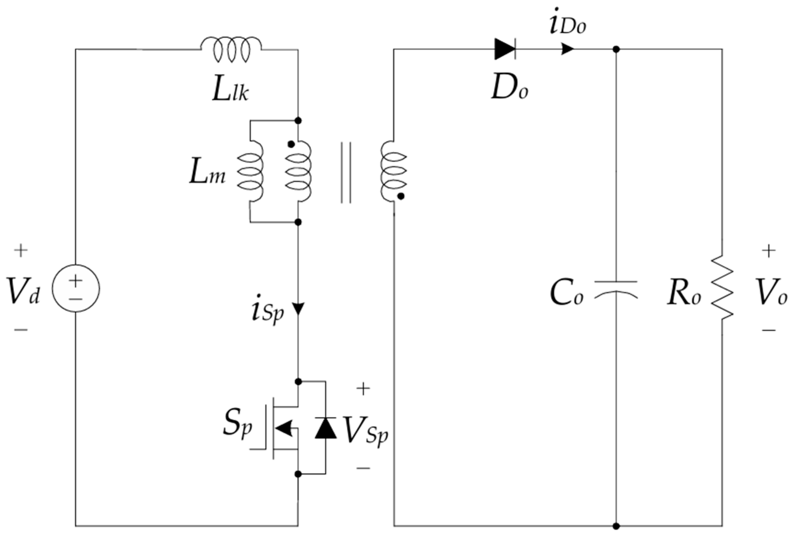
Figure 1. Circuit diagram of the conventional flyback converter.
Energies 17 04729 g001
Figure 2. Circuit diagram of the proposed flyback converter.
Energies 17 04729 g002
Figure 3. Operation modes of the proposed converter.
Energies 17 04729 g003
Figure 4. Operation waveforms of the proposed converter (Adapted with permission form [27]. Copyright 2023, John Wiley and Sons).
Energies 17 04729 g004
Figure 5. Normalized voltage gain curves.
Energies 17 04729 g005
Figure 6. Operation waveforms of the proposed converter for the exceptional design case.
Energies 17 04729 g006
Figure 7. Simulation waveforms of the conventional converter: (a) VSp and iSp; (b) VSp and iDo.
Energies 17 04729 g007aEnergies 17 04729 g007b
Figure 8. Simulation waveforms of the proposed converter: (a) VSp and iSp; (b) iDo and iDa.
Energies 17 04729 g008aEnergies 17 04729 g008b
Figure 9. Pictures for the experimental setup: (a) test environment; (b) digital power meter.
Energies 17 04729 g009
Figure 10. Circuit diagram for the control circuit implementation.
Energies 17 04729 g010
Figure 11. Experimental waveforms of the conventional converter: (a) VSp and iSp; (b) VSp and iSp.
Energies 17 04729 g011
Figure 12. Experimental waveforms of the proposed converter: (a) VSp and iSp; (b) VSp and iSp.
Energies 17 04729 g012
Figure 13. Experimental waveforms of the conventional converter: (a) VSp and iDo; (b) VSp and iDo; (c) VDo and iDo.
Energies 17 04729 g013
Figure 14. Experimental waveforms of the proposed converter: (a) iDo and iDa; (b) VSp and iDa; (c) VSp and iDa; (d) VDo and iDo; (e) VDa and iDa; (f) Vo and Io.
Energies 17 04729 g014
Figure 15. Measured power efficiency curves: (a) for different output power levels; (b) for different inductances of La in the proposed converter.
Energies 17 04729 g015
Figure 16. Power loss distributions for the proposed converter.
Energies 17 04729 g016
Figure 17. Measured power efficiency curves: (a) for the 45 W rated load condition; (b) for the 90 W rated load condition.
Energies 17 04729 g017
Figure 18. Circuit diagram of the proposed converter applied for the single-stage single-switch power factor correction.
Energies 17 04729 g018
Table 1. Electrical specifications and the circuit parameters.
SymbolQuantityValue
Vdinput voltage48 V
Vooutput voltage15 V
Porated output power45 W
fsswitching frequency50 kHz
Lmmagnetizing inductance300 μH
Llkleakage inductance1 μH
Sppower switchIRF640NPbF
Dooutput diodeMBR10100G
Daadditional diodeMBR10100G
Laadditional inductor7 μH
Cooutput capacitor2200 μF
Table 2. Comparison of the electrical specifications and the power efficiency for previous converters.
Input Voltage/Output VoltageRated Output PowerPower Efficiency
[18]50 V/100 V200 Wnot announced
[19]140 V/24 V100 W90.5%
[20]72 V/12 V100 W77.5%
Table 3. Comparison of different passive snubber methods with the proposed method.
ComponentAdvantageComplexity
Lossless snubber [18]inductor × 2,
diode × 4,
capacitor × 1,
coupled
inductor × 1
zero-voltage turn-on (switch),
zero-current-turn-off (diode)
high
Lossless snubber [19]capacitor × 2,
diode × 4,
coupled
inductor × 1
zero-voltage turn-on (switch),
zero-current-turn-off (diode)
high
Regenerative snubber [20]capacitor × 1,
diode × 3,
coupled
inductor × 1
zero-voltage turn-on (switch),
energy regeneration
high
Proposed methodinductor × 1,
diode × 1,
transformer
winding × 1
zero-current turn-off (diode),
reduced turn-on loss (switch)
low
Table 4. Comparison of the flyback converters for the single-stage power factor corrections.
OperationAdvantageComplexity
Converter in [31]APWM
operation
(switch × 2)
Zero-voltage
switching (switch)
medium
Converter in [32]BCM
operation
(switch × 5)
Zero-current
switching (diode)
high
Proposed converter in Figure 18CCM
Operation
(switch × 1)
Zero-current
switching (diode)
low
Disclaimer/Publisher’s Note: The statements, opinions and data contained in all publications are solely those of the individual author(s) and contributor(s) and not of MDPI and/or the editor(s). MDPI and/or the editor(s) disclaim responsibility for any injury to people or property resulting from any ideas, methods, instructions or products referred to in the content.