1. Introduction
Semiconductor devices interacting with high-energy particles in the space radiation environment are susceptible to ionization that may lead to temporal functional interruptions or long-term degradation. Total Ionizing Dose and Displacement Damage Dose are long-term radiation effects resulting from trapped charges on the oxide layers of silicon devices [
1,
2,
3]. These long-term radiation effects may induce the parametric degradation of semiconductor devices regarding threshold shift, gain reduction, increase leakage current, etc., and even complete functional disruption [
4,
5,
6].
X-rays and gamma radiation produced by high-energy photons, such as
60Co, are commonly employed sources for emulating the Total Dose received at space level [
7,
8,
9]. The interaction of semiconductors with charged particles also leads to temporal malfunction or glitches in analog devices, generally categorized as Single-Event Transients (SETs). These transient glitches may lead to functional interruptions or distortions, generally known as Single-Event Functional Interruptions (SEFI) [
10,
11,
12,
13,
14,
15,
16]. High-energy particle beams, such as protons or heavy ions, are commonly used to emulate these transient radiation effects at ground level [
16,
17,
18,
19,
20].
Previous studies have revealed that pulsed lasers are a reliable alternative to traditional particle testing when it comes to fault injection experiments. Despite the complexity of finding a correlation between pulse energy and the LET of charge particles [
20], pulsed lasers provide high control in terms of injection time and energy, in addition to high scan resolution, allowing for simpler debugging of sensitive nodes or regions, as well as the identification of threshold levels [
17,
18,
19,
20,
21].
This work is dedicated to studying the response of the AD524CDZ instrumentation amplifier to long- and short-term radiation exposure. Long-term effects were evaluated using a low-dose 60Co chamber to emulate the space radiation environment. SEE response was tested using proton radiation and two-photon absorption (TPA) lasers. Moreover, TPA laser experiments were employed to identify sensitive regions within this Commercial-Off-The-Shelf (COTS) amplifier and correlate the SET response of this device under different gain setups.
2. Device-under-Testing Setup Overview
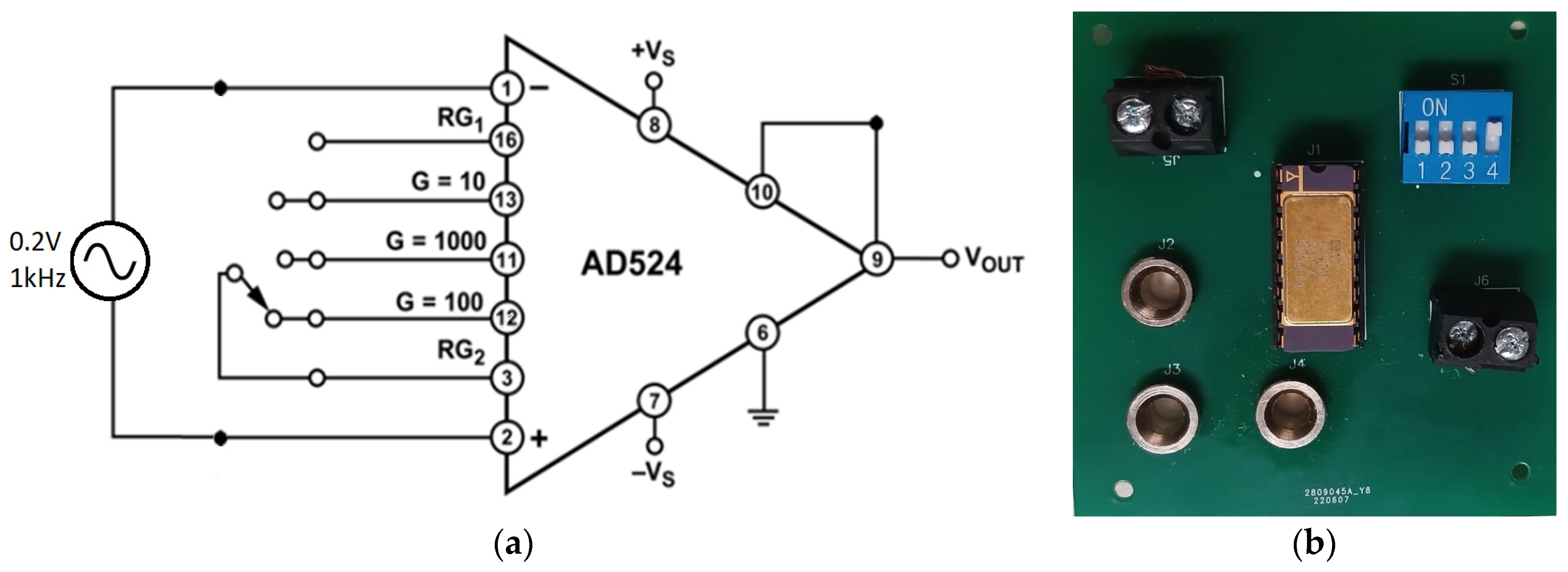
The device under testing (DUT) selected for this study was the AD524CDZ precision instrumentation amplifier manufactured by Analog Devices Inc on a bipolar process. This instrumentation amplifier contains internal resistors for pin-programmable gains of 1, 10, 100, and 1000 and operates within a temperature range of −40 °C to 85 °C [
22].
Figure 1a shows the general schematic employed to measure the response of the selected device against TID and SEE.
Figure 1b shows the fabricated test board used for the different experiments.
3. Total Ionizing Dose Experiments
The Total Ionizing Dose (TID) study was carried out using a low-dose-rate
60Co chamber. Since the selected DUT was fabricated using bipolar technology, a low dose rate was selected due to the propensity of bipolar devices to exhibit Enhanced Low-Dose-Rate Sensitivity (ELDRS) [
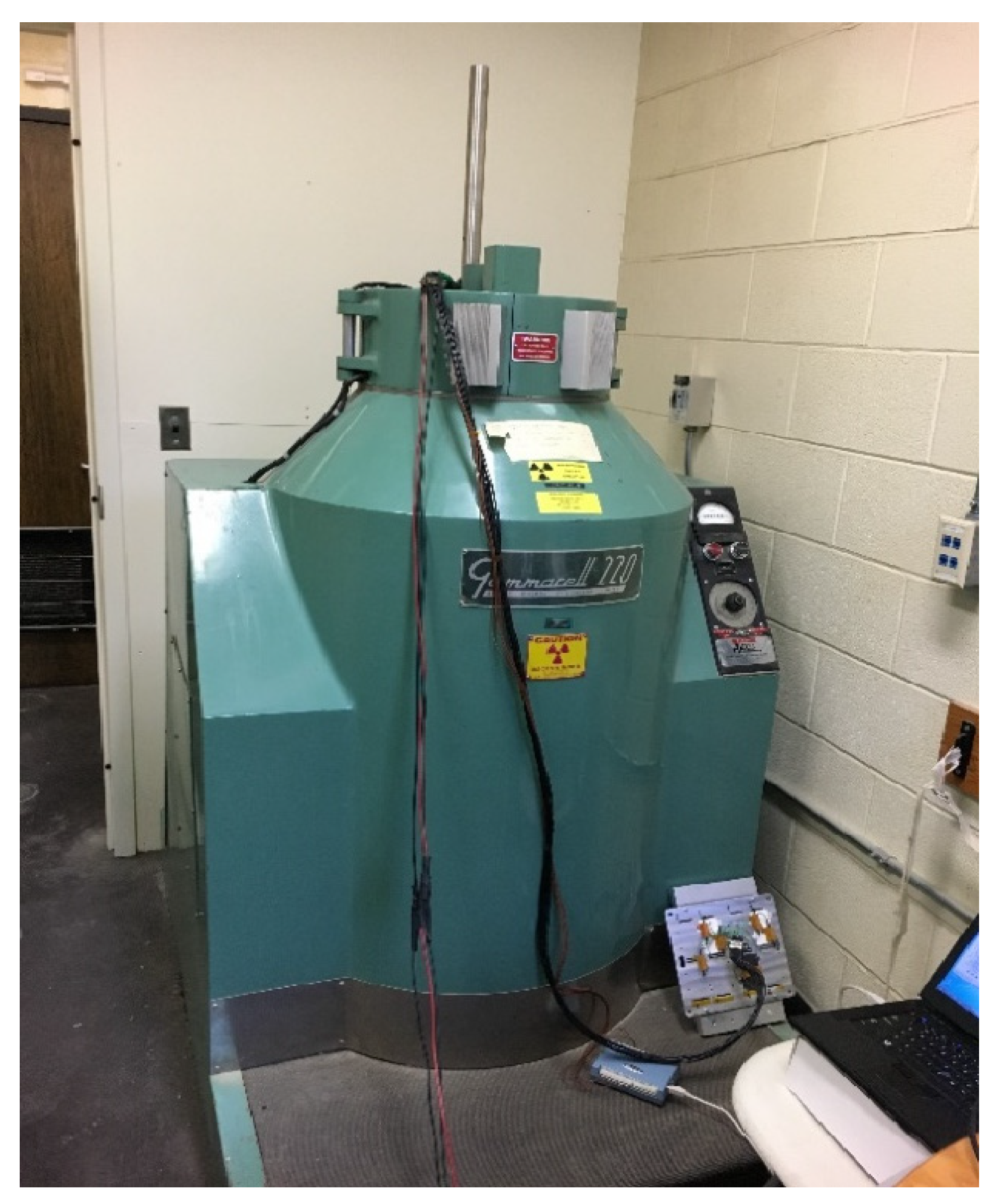
23]. The Gammacell 220 illustrated in
Figure 2 is located at the University of Saskatchewan and currently generates 2.51 rad/min of irradiation at the center of the chamber. Three samples of the DUT were irradiated up to a target dose of 100 krad. Each sample board was set to 100× gain and different inputs.
On the first test board, a 1 kHz sinewave input with a 200 mV peak–peak amplitude was connected to the amplifier’s inputs (pins 1 and 2, as shown in
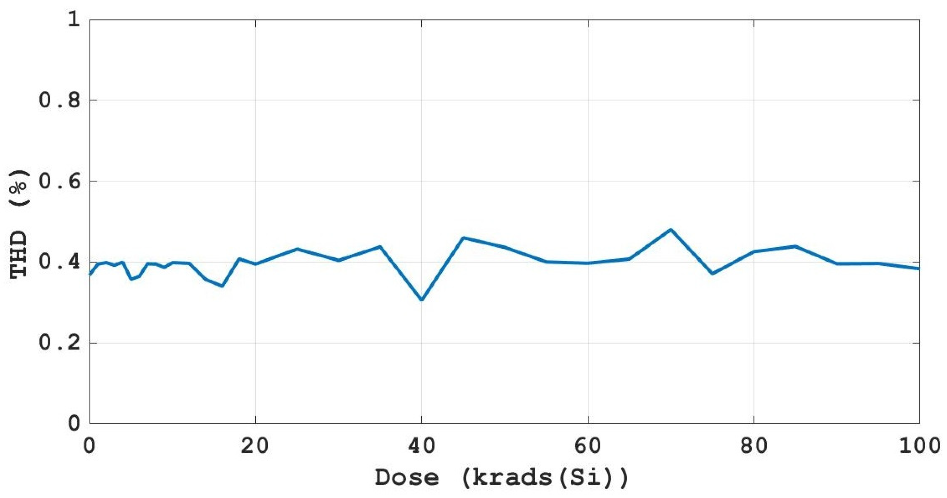
Figure 1). An oscilloscope was used to capture the output waveform and measure the parametric peak-to-peak output voltage throughout the experiment. Total Harmonic Distortion (THD) was calculated using the signal-processing toolbox from MATLAB.
The results presented in
Figure 3 and
Figure 4 revealed that the device did not show major parametric drift. The Total Harmonic Distortion showed no significant signal compression, presenting values within the specifications [
22], and hence the peak-to-peak output amplitude remained unchanged up to the target dose.
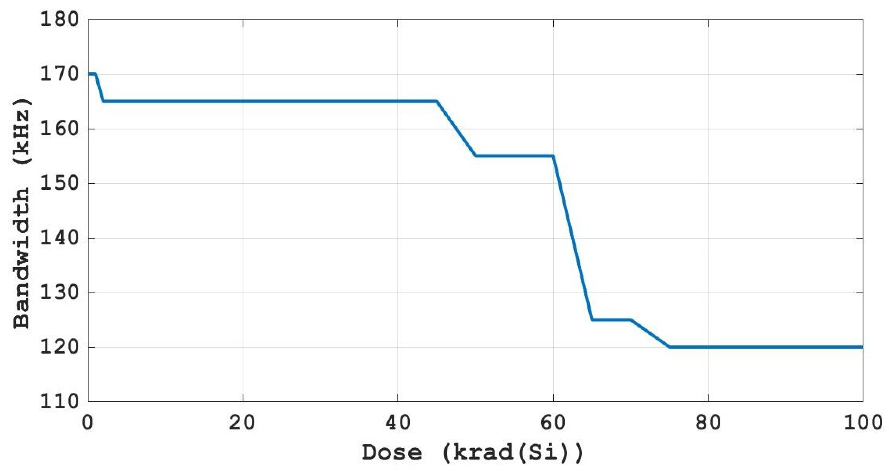
A second sample of the DUT was used to measure bandwidth. The input of the second board was initially set to the same 1 kHz sinewave input with a 200 mV peak–peak amplitude. The frequency of the input signal was increased to 180 kHz (in steps of 5 kHz) to characterize the frequency response of the DUT. An oscilloscope was used to identify the frequency (bandwidth) at which the output amplitude fell to half of its maximum value. The results presented in
Figure 5 show a significant drop in the bandwidth at about 60 krad; however, it stabilized again and remained this way up to the target dose. Despite the drift, the reported values remain with the specifications reported in the datasheet of the DUT [
22]
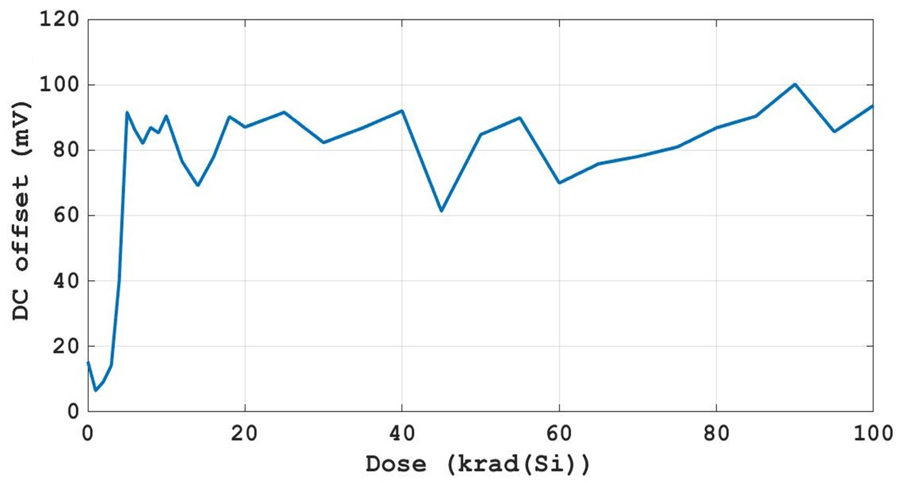
For the DC offset measurement, both inverting and non-inverting inputs of the third sample were tied to the ground. Similar to the previous case, the results revealed the DC offset levels remained within the vendor’s specifications [
22], showing that the device is functional up to 100 krad, as depicted in
Figure 6.
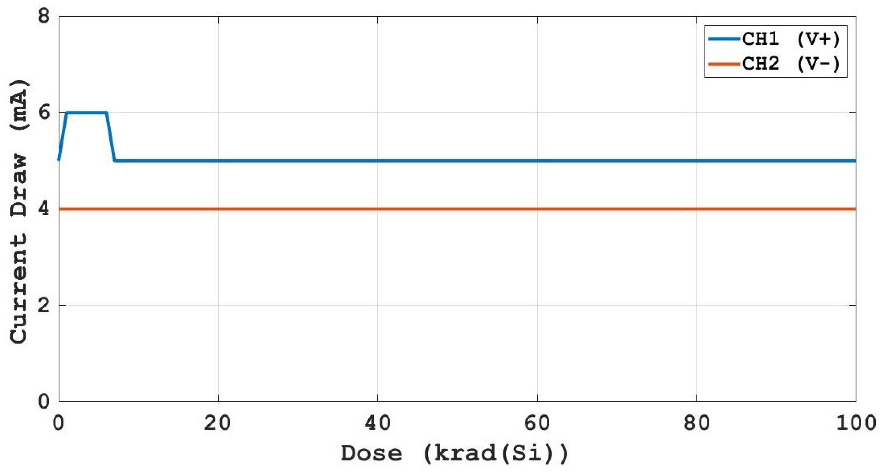
The current draw from positive and negative supplies was tracked throughout the experiment. The results presented in
Figure 7 show no alteration in the current-consumption levels up to 100 krad(Si).
4. SEE Experiments Using a Proton Beam
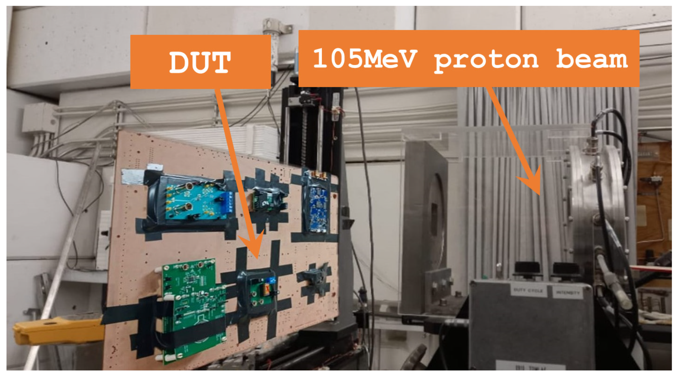
The first approach of SEE testing was carried out at the TRIUMF Proton Irradiation Facility located on the UBC campus. A 105 MeV beam energy with a 1 nA beam current was used to irradiate the DUT up to a target fluence of 2 × 10
10 proton/cm
2. The gain of the AD524CDZ was set at 100×, and the inputs were tied to ground. The output was measured to look for transients in the DC offset. The experimental setup is presented in
Figure 8.
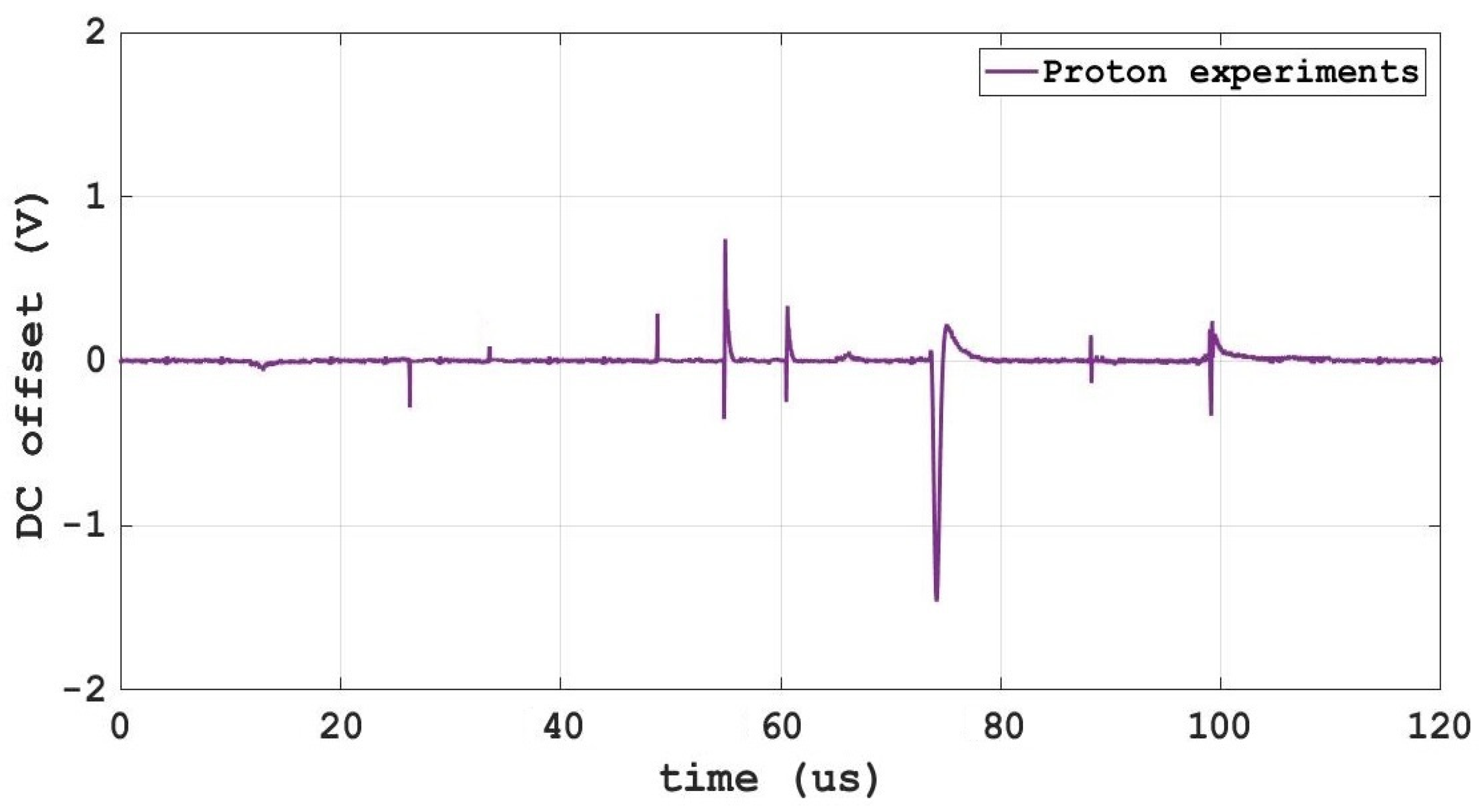
The results from the proton experiment presented in
Figure 9 revealed a cross-section of 7.52 × 10
−10 with a maximum DC offset glitch of about 1.5 V.
Additionally,
Figure 9 reveals that although several SET glitches were detected throughout the proton irradiation experiment, the DUT was able to recover normal functionality once the collected charge had dissipated.
5. SEE Experiments Using Two-Photon Laser
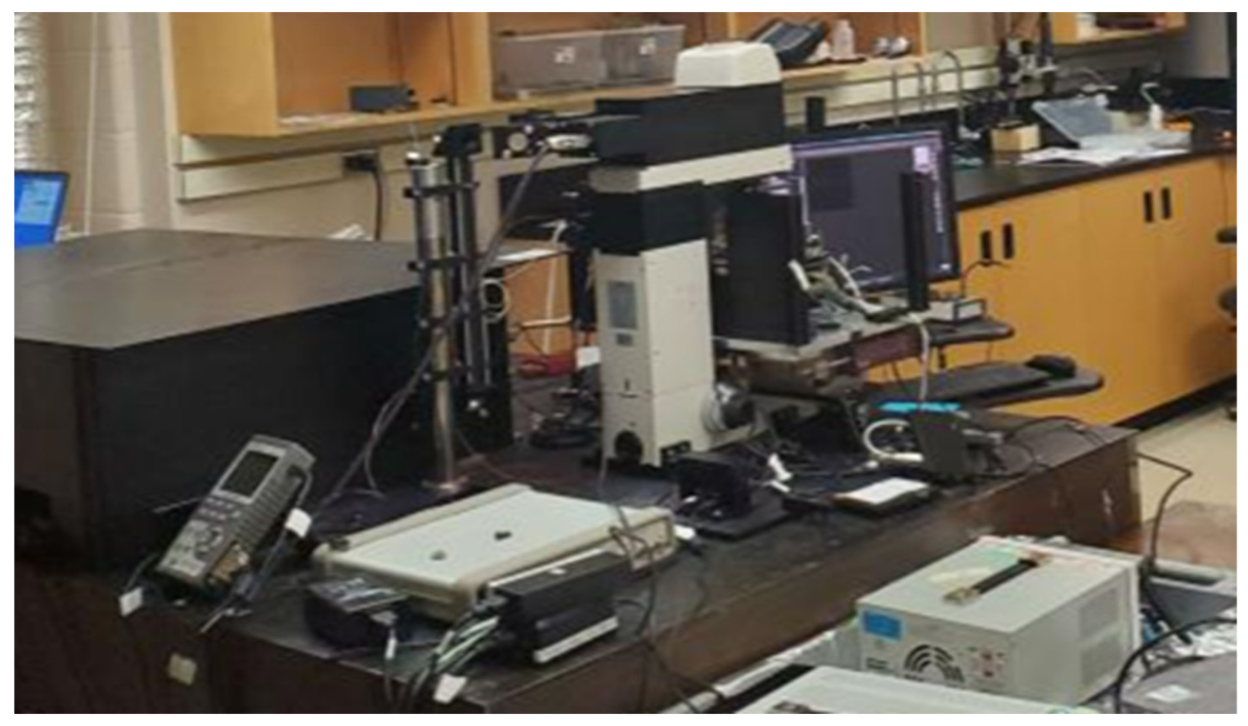
The second set of SEE experiments was conducted at the optics laboratory at the University of Saskatchewan. A two-photon absorption (TPA) laser facility (shown in
Figure 10) was employed to inject different levels of pulse energy at different sectors of the die using different gain configurations.
The sample preparation step for this experiment was straightforward, as the de-lidding process did not require wet etching or a milling process to expose the DIE.
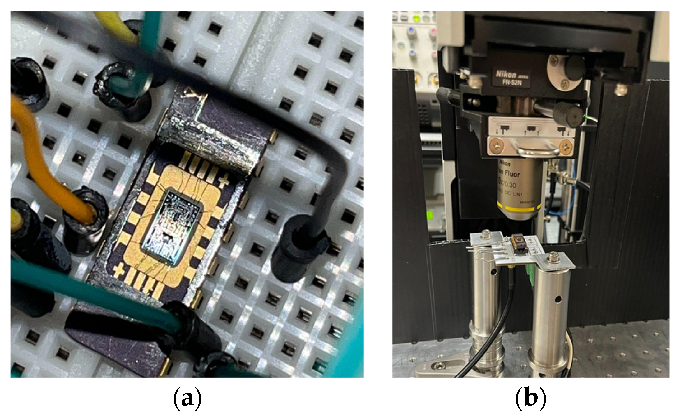
Figure 11a shows a close-up of the de-lidded DUT with the exposed die. The selected DUT is a mature product with low-density top metal interconnection layers, which allows for top-side laser injection without requiring further polishing or a thinning process. The DUT mounted on the microscope platform for laser injection is shown in
Figure 11b.
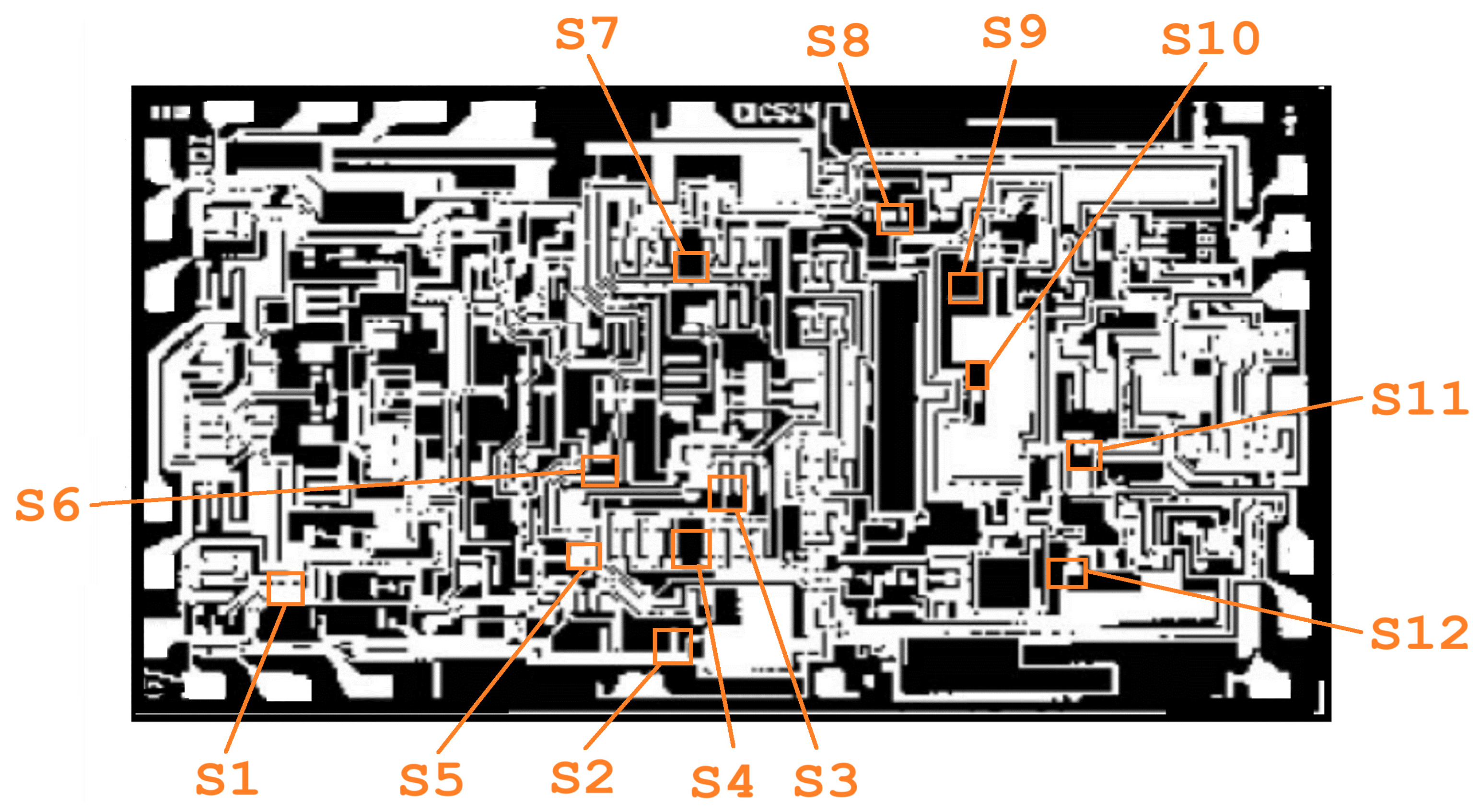
SETs at the output were the parameters of interest for all the laser experiments, and the inputs of the instrumentation amplifier were grounded. For the first run, the gain of the AD524CDZ was set to 100×. Different levels of laser energy were used to scan the die and thus identify sensitive sectors (shown in
Figure 12).
The first iteration of the laser experiments helped to identify the different thresholds of laser energy required for the observation of SETs in each sensitive sector. The results summarized in
Table 1 revealed that Sectors 1, 3, 4, 10, and 12 are the most sensitive, with a 0.1 nJ threshold energy. Moreover,
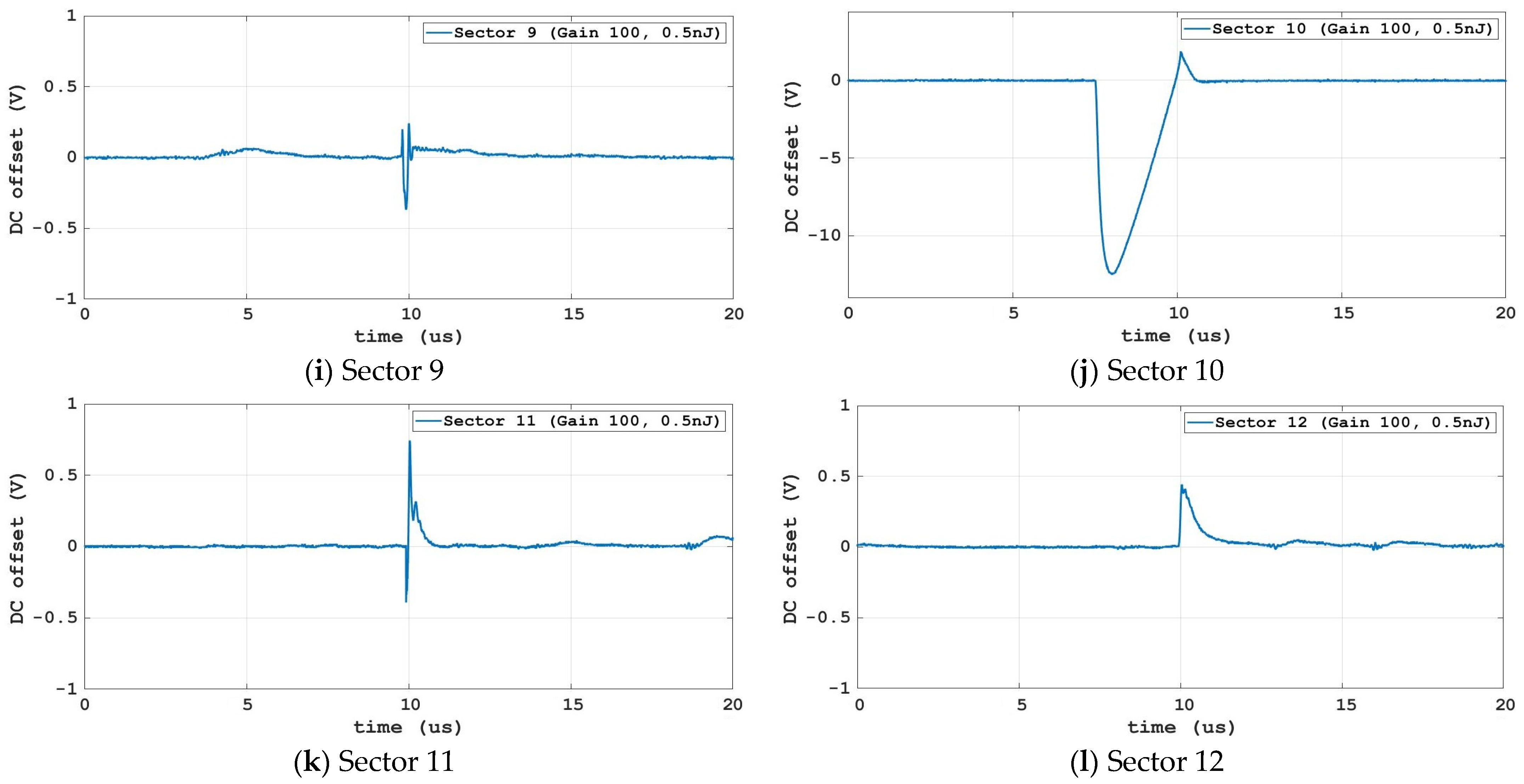
Table 1 also shows that the greatest amount of energy required to disturb some of the sensitive areas was 0.5 nJ. To identify the most-sensitive areas of the die (i.e., the areas that generate the largest SET) under the same laser energy level, a second round of laser experiments was conducted using 0.5 nJ of laser energy to scan the different sensitive sectors previously identified. A 100× gain setup was employed for this experiment.
The results presented in
Figure 13 demonstrate that under the same injected energy, Sectors 4 and 10 exhibit the largest SET. Furthermore, Sector 10 is highlighted as the most-sensitive area, with a 13.3 V SET glitch and a 3.07 us recovery time. The results from the second round of laser injection are summarized in
Table 2.
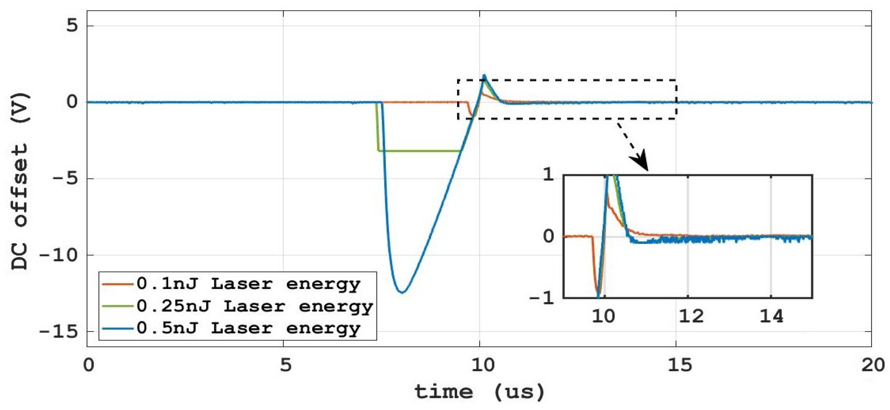
Additional laser injection experiments were carried out only in Sector 10 to characterize how different laser energies and different gain setups affect the SET response of the studied instrumentation amplifier. For the third round of laser testing, the DUT was set to 100× gain. Sector 10 was scanned using three different laser energies (0.1 nJ, 0.25 nJ, and 0.5 nJ). The results presented in
Figure 14 show that there is a direct relationship between the magnitude of the SET in the DC amplitude and the injected energy. Injecting a greater amount of laser energy will also increase the time the DUT requires to resume normal operation.
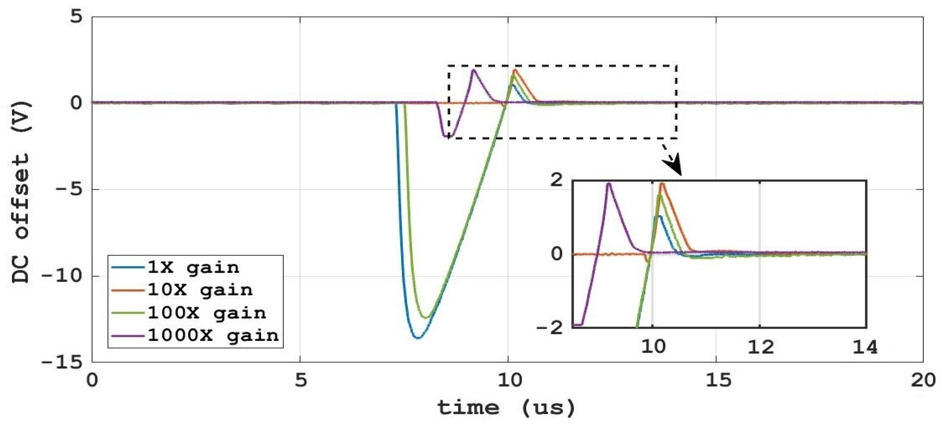
Finally, the last round of laser experiments, which involved finding how different DC gains may affect the response of the DUT, was conducted. For this part of the test, a fixed laser energy level of 0.5 nJ was used to scan Sector 10 while using different gain setups (1×, 10×, 100×, and 1000×).
The results depicted in
Figure 15 show that the magnitude of the SET was considerably reduced when using 10× and 1000×. This SET magnitude reduction may be attributed to the bandwidth reduction induced by increasing the closed loop gain, which helps to attenuate the SET. However, this is not the case for the 100× gain setup, which showed no improvement in the SEE response. This behavior can be attributed to instability problems due to an insufficient phase margin at 100× gain.
6. Discussion
As shown by the experimental data, the selected instrumentation amplifier exhibits robust functionality under radiation stress. In terms of TID, the DUT presented high robustness with limited performance degradation regarding output peak-to-peak amplitude, THD, and DC offset. Even though there was a significant drift in the amplifiers’ bandwidth due to long-term exposure to radiation, the reported value at the target dose remained aligned with the manufacturer’s specifications.
With regard to SEE, the DUT was easily upset by proton radiation; however, the glitches produced were not critical enough to generate a functional interruption. Moreover, the tested instrumentation amplifier was able to recover normal functionality without the need for power cycling. While it is true that the SEE response was characterized only in terms of DC offset, significant information regarding the SEE response of the DUT when different gain setups are employed was collected from the laser experiments, showing that the use of a higher gain will contribute to reducing the SET magnitude and improving the recovery time.
Thus, this study demonstrates that the AD524CDZ instrumentation amplifier is a suitable option for space applications within both Low Earth Orbit (LEO) and Medium Earth Orbit (MEO). The selected devices not only show high robustness to (TID) effects but also present self-recovery capabilities with respect to Single-Event Transients (SETs), ensuring reliable performance without requiring a power cycle process.
7. Conclusions
This article presents the characterization of the radiation response of the COTS AD524CDZ instrumentation amplifier. The results from the TID and SEE experiments reveal the studied device exhibits high radiation tolerance. No major performance degradation was observed, and the part was still functional after 100 krads.
In terms of SEE performance, the AD524CDZ instrumentation amplifier presented a good response to proton radiation; the device remained functional after 2 × 10¹⁰ fluence was reached, showing an error cross section of 7.52 × 10⁻¹⁰. The laser tests revealed that even though some large SEEs were observed in some of the sensitive regions, the device was able to resume normal operation once the injected charge had dissipated. In addition, none of the transients were considerably long since they were all in the range of µs. As expected, there is a direct relationship between the beam energy injected and the DC transient magnitude. However, the robustness of the selected DUT improves when using different gain levels. When increasing the closed loop gain, the bandwidth drops, and because of this transient, it becomes somewhat attenuated.
In conclusion, based on the presented results, the AD524CDZ instrumentation amplifier is a suitable tool and robust enough for operation in the space radiation environment.
Author Contributions
Conceptualization, D.H. and J.C.C.; methodology, J.C.C.; experimental process, J.C.C., A.N.C., B.J. and D.B.; formal analysis, J.C.C.; investigation, J.C.C.; resources, L.C.; writing—original draft preparation, J.C.C.; writing—review and editing, L.C.; supervision, L.C.; project administration, L.C.; funding acquisition, L.C. All authors have read and agreed to the published version of the manuscript.
Funding
This work was supported by MDA internal research and development and the Canada Natural Science and Engineering Research Council (NSERC).
Data Availability Statement
The data presented in this study are available on request from the corresponding author. The data are not publicly available due to licensing agreements.
Conflicts of Interest
The authors declare no conflicts of interest.
References
- Maurer, R.H.; Fraeman, M.E.; Martin, M.N.; Roth, D.R. Harsh Environments: Space Radiation Environment, Effects, and Mitigation. Johns Hopkins APL Tech. Dig. 2008, 28, 17. [Google Scholar]
- Schwank, J.R.; Shaneyfelt, M.R.; Fleetwood, D.M.; Felix, J.A.; Dodd, P.E.; Paillet, P.; Ferlet-Cavrois, V. Radiation Effects in MOS Oxides. IEEE Trans. Nucl. Sci. 2008, 55, 1833–1853. [Google Scholar] [CrossRef]
- Hughes, H.L.; Benedetto, J.M. Radiation effects and hardening of MOS technology: Devices and circuits. IEEE Trans. Nucl. Sci. 2003, 50, 500–521. [Google Scholar] [CrossRef]
- İlic, S.; Yelten, M.B. Total Ionizing Dose (TID) Impact on Basic Amplifier Stages. IEEE Trans. Device Mater. Reliab. 2023, 23, 51–57. [Google Scholar] [CrossRef]
- Ding, H.; Cui, J.; Zheng, Q.; Xu, H.; Gao, N.; Xun, M.; Yu, G.; He, C.; Li, Y.; Guo, Q. Effect of Trapped Charge Induced by Total Ionizing Dose Radiation on the Top-Gate Carbon Nanotube Field Effect Transistors. Electronics 2023, 12, 1000. [Google Scholar] [CrossRef]
- Oldham, T.R.; McLean, F.B. Total ionizing dose effects in mos oxides and devices. IEEE Trans. Nucl. Sci. 2003, 50, 483–499. [Google Scholar] [CrossRef]
- MIL-STD-883EMethod 1019.4 Ionizing Radiation (Total Dose) Test Procedure. 15 November 1991.
- Menicucci, A. Simplified Procedures for COTS TID Testing: A Comparison between 90Sr and 60Co. In Proceedings of the 2018 IEEE Radiation Effects Data Workshop (REDW), Waikoloa, HI, USA, 16–20 July 2018; IEEE: New York, NY, USA, 2018; pp. 1–6. [Google Scholar]
- Kniffin, S.; Palor, C. Total Ionizing Dose (TID) Test Report for the MAX6325; NASA GSFC Radiation Effects Facility: Greenbelt, MD, USA, 2003. [Google Scholar]
- Turflinger, T.L. Single-event effects in analog and mixed-signal integrated circuits. IEEE Trans. Nucl. Sci. 1996, 43, 594–602. [Google Scholar] [CrossRef]
- Wirth, J.; Rogers, S. The Transient Response of Transistors and Diodes to Ionizing Radiation. IEEE Trans. Nucl. Sci. 1964, 5, 24–38. [Google Scholar] [CrossRef]
- Long, D.M.; Florian, J.; Casey, R.H. Transient Response Model for Epitaxial Transistors. IEEE Trans. Nucl. Sci. 1983, 30, 4131–4134. [Google Scholar] [CrossRef]
- Koga, R.; Kolasinski, W.; Imamoto, S. Heavy Ion Induced Upsets in Semiconductor Devices. IEEE Trans. Nucl. Sci. 1985, 32, 159–162. [Google Scholar] [CrossRef]
- Koga, R.; Pinkerton, S.; Moss, S.; Mayer, D.; LaLumondiere, S.; Hansel, S.; Crawford, K.; Crain, W. Observation of Single Event Upsets in Analog Microcircuits. IEEE Trans. Nucl. Sci. 1993, 40, 1838–1844. [Google Scholar] [CrossRef]
- Wang, H.B.; Liu, R.; Li, X.-T.; Chen, L.; Hiemstra, D.M.; Kirischian, V. Total ionizing dose test facilities for micro-electronic circuits. In Proceedings of the 2016 IEEE Canadian Conference on Electrical and Computer Engineering (CCECE), Vancouver, BC, Canada, 3 November 2016; IEEE: New York, NY, USA; pp. 1–4. [Google Scholar]
- Budroweit, J. Proton Induced Single Event Effect Characterization on a Highly Integrated RF-Transceiver. Electronics 2019, 8, 519. [Google Scholar] [CrossRef]
- Melinger, J.S.; Buchner, S.; McMorrow, D.; Stapor, W.J.; Weatherford, T.R.; Campbell, A.B. Critical evaluation of the pulsed laser method for single event effects testing and fundamental studies. IEEE Trans. Nucl. Sci. 1994, 41, 2574–2584. [Google Scholar] [CrossRef]
- Moss, S.C.; LaLumondiere, S.D.; Scarpulla, J.R.; MacWilliams, K.P.; Crain, W.; Koga, R. Correlation of picosecond laser-induced latchup and energetic particle induced latchup in CMOS test structures. IEEE Trans. Nucl. Sci. 1995, 42, 1948–1956. [Google Scholar] [CrossRef]
- McMorrow, D.; Melinger, J.; Buchner, S.; Scott, T.; Brown, R.D.; Haddad, N. Application of a pulsed laser for evaluation and optimization of SEU-hard designs. IEEE Trans. Nucl. Sci. 2000, 47, 559–565. [Google Scholar] [CrossRef]
- Huang, J.; Han, J. Calculation of LET in SEE simulation by pulsed laser. Sci. China Ser. G. Phys. Mech. Astron. 2005, 48, 113–121. [Google Scholar] [CrossRef]
- McMorrow, D.; Lotshaw, W.; Melinger, J.; Pease, R. Sub bandgap Laser-Induced Single Event Effects: Carrier Generation via Two-Photon Absorption. IEEE Trans. Nucl. Sci. 2002, 49, 3002–3008. [Google Scholar] [CrossRef]
- Analog Devices, “Datasheet AD524”, Rev H. 2023. Available online: https://www.analog.com/media/en/technical-documentation/data-sheets/ad524.pdf (accessed on 20 August 2024).
- Boch, J.; Michez, A.; Rousselet, M.; Dhombres, S.; Touboul, A.D.; Vaillé, J.-R.; Dusseau, L.; Lorfèvre, E.; Chatry, N.; Sukhaseum, N.; et al. Dose Rate Switching Technique on ELDRS-Free Bipolar Devices. IEEE Trans. Nucl. Sci. 2016, 63, 2065–2071. [Google Scholar] [CrossRef]
| Disclaimer/Publisher’s Note: The statements, opinions and data contained in all publications are solely those of the individual author(s) and contributor(s) and not of MDPI and/or the editor(s). MDPI and/or the editor(s) disclaim responsibility for any injury to people or property resulting from any ideas, methods, instructions or products referred to in the content. |
© 2024 by the authors. Licensee MDPI, Basel, Switzerland. This article is an open access article distributed under the terms and conditions of the Creative Commons Attribution (CC BY) license (https://creativecommons.org/licenses/by/4.0/).
