
Concept of Enabling Over-Current Capability of Silicon-Carbide-Based Power Converters with Gate Voltage Augmentation


Abstract
1. Introduction
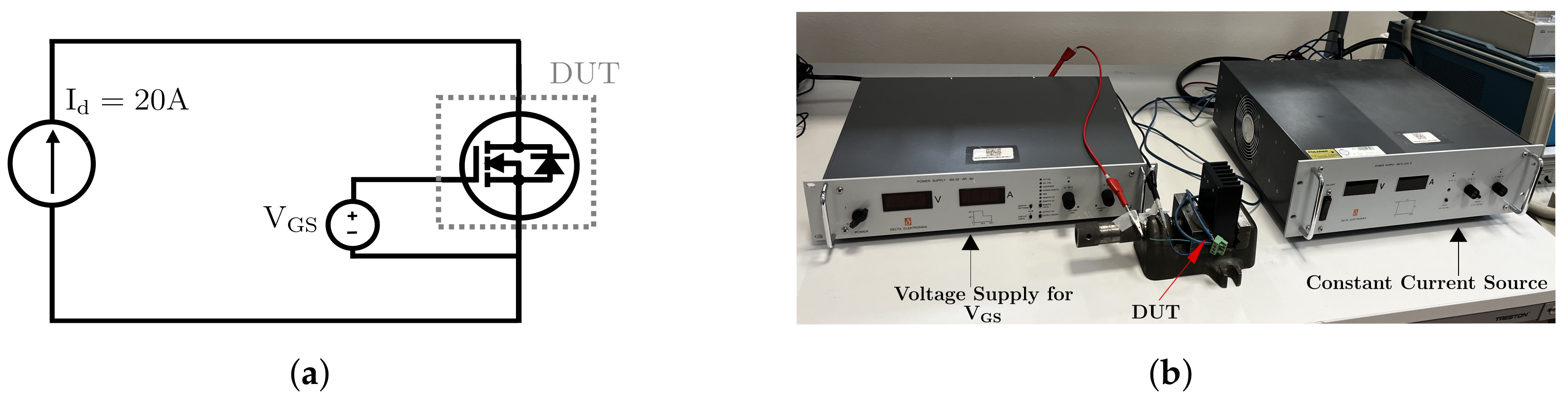
2. Simulation and Experiment
3. Proposed Driver
4. Discussion
5. Conclusions
Author Contributions
Funding
Data Availability Statement
Conflicts of Interest
Abbreviations
| Gate voltage | |
| MOSFET | Metal-oxide semiconductor field-effect transistor |
| OC | Over-current |
| SiC | Silicon carbide |
References
- Abbott, D. Keeping the Energy Debate Clean: How Do We Supply the World’s Energy Needs? Proc. IEEE 2010, 98, 42–66. [Google Scholar] [CrossRef]
- 1668-2017; IEEE Recommended Practice for Voltage Sag and Short Interruption Ride-Through Testing for End-Use Electrical Equipment Rated Less than 1000 V. IEEE: Piscataway, NJ, USA, 2017.
- Shao, W.; Wu, R.; Ran, L.; Jiang, H.; Mawby, P.A.; Rogers, D.J.; Green, T.C.; Coombs, T.; Yadley, K.; Kastha, D.; et al. A Power Module for Grid Inverter with in-built Short-Circuit Fault Current Capability. IEEE Trans. Power Electron. 2020, 35, 10567–10579. [Google Scholar] [CrossRef]
- Bhadoria, S.; Dijkhuizen, F.; Raj, R.; Wang, X.; Xu, Q.; Matioli, E.; Kostov, K.; Nee, H.P. Enablers for Overcurrent Capability of Silicon-Carbide-Based Power Converters: An Overview. IEEE Trans. Power Electron. 2023, 38, 3569–3589. [Google Scholar] [CrossRef]
- Zhang, C.; Liu, Q.; Zhou, B.; Chung, C.Y.; Li, J.; Zhu, L.; Shuai, Z. A Central Limit Theorem-Based Method for DC and AC Power Flow Analysis Under Interval Uncertainty of Renewable Power Generation. IEEE Trans. Sustain. Energy 2023, 14, 563–575. [Google Scholar] [CrossRef]
- Wang, D.; Zhang, C.; Li, J.; Zhu, L.; Zhou, B.; Zhou, Q.; Cheng, L.; Shuai, Z. A Novel Interval Power Flow Method Based on Hybrid Box-Ellipsoid Uncertain Sets. IEEE Trans. Power Syst. 2024, 39, 6111–6114. [Google Scholar] [CrossRef]
- Gomis-Bellmunt, O.; Sau-Bassols, J.; Prieto-Araujo, E.; Cheah-Mane, M. Flexible Converters for Meshed HVDC Grids: From Flexible AC Transmission Systems (FACTS) to Flexible DC Grids. IEEE Trans. Power Deliv. 2020, 35, 2–15. [Google Scholar] [CrossRef]
- Imdadullah; Amrr, S.M.; Jamil Asghar, M.S.; Ashraf, I.; Meraj, M. A Comprehensive Review of Power Flow Controllers in Interconnected Power System Networks. IEEE Access 2020, 8, 18036–18063. [Google Scholar] [CrossRef]
- Guo, H.; Chen, W.; Zhu, Y.; Zhu, M. An Expandable Interline DC Power Flow Controller. IEEE Trans. Power Electron. 2024, 39, 826–836. [Google Scholar] [CrossRef]
- Zhang, X.; Yang, J.; Wu, Z.; Zhang, B.; Qi, L. A Novel Thyristor-Controlled Voltage-Source-Based Forced Resonant Mechanical DC Circuit Breaker. IEEE Trans. Power Electron. 2023, 38, 14563–14572. [Google Scholar] [CrossRef]
- Colmenares, J.; Peftitsis, D.; Rabkowski, J.; Sadik, D.; Tolstoy, G.; Nee, H.P. High-Efficiency 312-kVA Three-Phase Inverter Using Parallel Connection of Silicon Carbide MOSFET Power Modules. IEEE Trans. Ind. Appl. 2015, 51, 4664–4676. [Google Scholar] [CrossRef]
- Khazaka, R.; Mendizabal, L.; Henry, D.; Hanna, R. Survey of High-Temperature Reliability of Power Electronics Packaging Components. IEEE Trans. Power Electron. 2015, 30, 2456–2464. [Google Scholar] [CrossRef]
- Bhadoria, S.; Soundhariya, G.S.; Nee, H.P. Comparison of Short-Term Over-current Capability of SiC Devices using Microchannel Cooling below and on top of the Chip. In Proceedings of the 2024 IEEE 10th International Power Electronics and Motion Control Conference (IPEMC2024-ECCE Asia), Chengdu, China, 17–20 May 2024; pp. 356–362. [Google Scholar] [CrossRef]
- Bhadoria, S.; Dijkhuizen, F.; Zhang, X.; Ran, L.; Nee, H.P. Over-Current Capability of Silicon Carbide and Silicon Devices for Short Power Pulses with Copper and Phase Change Materials below the Chip. Energies 2024, 17, 462. [Google Scholar] [CrossRef]
- Bhadoria, S.; Soundhariya, G.S.; Nee, H.P. Comparison of Top and Bottom Cooling for Short Duration of Over-Currents for SiC| Devices: An Analysis of the Quantity and Location of Heat-Absorbing Materials. IEEE Open J. Power Electron. 2024, 5, 765–778. [Google Scholar] [CrossRef]
- Salmen, P.; Feil, M.; Waschneck, K.; Reisinger, H.; Rescher, G.; Voss, I.; Sievers, M.; Aichinger, T. Gate-switching-stress test: Electrical parameter stability of SiC MOSFETs in switching operation. Microelectron. Reliab. 2022, 135, 114575. [Google Scholar] [CrossRef]
- Reigosa, P.D.; Luo, H.; Iannuzzo, F. Implications of Ageing Through Power Cycling on the Short-Circuit Robustness of 1.2-kV SiC mosfets. IEEE Trans. Power Electron. 2019, 34, 11182–11190. [Google Scholar] [CrossRef]
- Ugur, E.; Yang, F.; Pu, S.; Zhao, S.; Akin, B. Degradation Assessment and Precursor Identification for SiC MOSFETs under High Temp Cycling. IEEE Trans. Ind. Appl. 2019, 55, 2858–2867. [Google Scholar] [CrossRef]
- Beier-Moebius, M.; Lutz, J. Breakdown of Gate Oxide of SiC-MOSFETs and Si-IGBTs under High Temperature and High Gate Voltage. In Proceedings of the PCIM Europe 2017; International Exhibition and Conference for Power Electronics, Intelligent Motion, Renewable Energy and Energy Management, Nuremberg, Germany, 16–18 May 2017; pp. 1–8. [Google Scholar]
- Gonzalez, J.O.; Alatise, O. Impact of the Gate Oxide Reliability of SiC MOSFETs on the Junction Temperature Estimation Using Temperature Sensitive Electrical Parameters. In Proceedings of the 2018 IEEE Energy Conversion Congress Expo. (ECCE), Portland, OR, USA, 23–27 September 2018; pp. 837–844. [Google Scholar] [CrossRef]
- Yu, H.; Liang, S.; Wang, J.; Jiang, X.; Wang, B.; Yang, Y.; Wang, Y.; Chen, Y. Understanding the Degradation of 1.2-kV Planar-Gate SiC MOSFETs under Repetitive Over-Load Current Stress. IEEE J. Emerging Sel. Top. Power Electron. 2022, 10, 5070–5080. [Google Scholar] [CrossRef]
- Li, H.; Zhao, S.; Wang, X.; Ding, L.; Mantooth, H.A. Parallel Connection of Silicon Carbide MOSFETs—Challenges, Mechanism, and Solutions. IEEE Trans. Power Electron. 2023, 38, 9731–9749. [Google Scholar] [CrossRef]
- Naghibi, J.; Mohsenzade, S.; Mehran, K.; Foster, M.P. Gate Oxide Degradation Condition Monitoring Technique for High-Frequency Applications of Silicon Carbide Power MOSFETs. IEEE Trans. Power Electron. 2023, 38, 1079–1091. [Google Scholar] [CrossRef]
- Gu, Z.; Yang, M.; Yang, Y.; Liu, X.; Gao, M.; Qi, J.; Liu, W.; Han, C.; Geng, L.; Hao, Y. Comparative Study on High-Temperature Electrical Properties of 1.2 kV SiC MOSFET and JBS-Integrated MOSFET. IEEE Trans. Power Electron. 2024, 39, 4187–4201. [Google Scholar] [CrossRef]
- Lu, X.; Wang, L.; Yang, Q.; Yang, F.; Gan, Y.; Zhang, H. Investigation and Comparison of Temperature-Sensitive Electrical Parameters of SiC MOSFET at Extremely High Temperatures. IEEE Trans. Power Electron. 2023, 38, 9660–9672. [Google Scholar] [CrossRef]
- Karakaya, F.; Maheshwari, A.; Banerjee, A.; Donnal, J.S. An Approach for Online Estimation of On-State Resistance in SiC MOSFETs without Current Measurement. IEEE Trans. Power Electron. 2023, 38, 11463–11473. [Google Scholar] [CrossRef]
- Meng, X.; Zhang, M.; Feng, S.; Tang, Y.; Zhang, Y. Online Temperature Measurement Method for SiC MOSFET Device Based on Gate Pulse. IEEE Trans. Power Electron. 2024, 39, 4714–4724. [Google Scholar] [CrossRef]
- Liu, T.; Zhu, S.; White, M.H.; Salemi, A.; Sheridan, D.; Agarwal, A.K. Time-Dependent Dielectric Breakdown of Commercial 1.2 kV 4H-SiC Power MOSFETs. IEEE J. Electron Devices Soc. 2021, 9, 633–639. [Google Scholar] [CrossRef]
- Yu, R.; Jahdi, S.; Mellor, P.; Liu, L.; Yang, J.; Shen, C.; Alatise, O.; Ortiz-Gonzalez, J. Degradation Analysis of Planar, Symmetrical and Asymmetrical Trench SiC MOSFETs under Repetitive Short Circuit Impulses. IEEE Trans. Power Electron. 2023, 38, 10933–10946. [Google Scholar] [CrossRef]
- Kang, J.; Zhu, A.; Chen, Y.; Luo, H.; Yao, L.; Xin, Z. An Online Gate Oxide Degradation Monitoring Method for SiC MOSFETs with Contactless PCB Rogowski Coil Approach. IEEE Trans. Power Electron. 2023, 38, 9673–9684. [Google Scholar] [CrossRef]
- Wang, M.; Chen, Y.; He, Z.; Wu, Z.; Li, B. Comparative Investigation on Aging Precursor and Failure Mechanism of Commercial SiC MOSFETs under Different Power Cycling Conduction Modes. IEEE Trans. Power Electron. 2023, 38, 7142–7155. [Google Scholar] [CrossRef]
- Wei, J.; Wei, Z.; Fu, H.; Cao, J.; Wu, T.; Sun, J.; Zhu, X.; Li, S.; Zhang, L.; Liu, S.; et al. Review on the Reliability Mechanisms of SiC Power MOSFETs: A Comparison Between Planar-Gate and Trench-Gate Structures. IEEE Trans. Power Electron. 2023, 38, 8990–9005. [Google Scholar] [CrossRef]
- Shuvra, M.A.; Del Rosso, A. Root Cause Identification of Power System Faults using Waveform Analytics. In Proceedings of the 2018 Clemson University Power System Conference (PSC), Charleston, SC, USA, 4–7 September 2018; pp. 1–8. [Google Scholar] [CrossRef]
- Ibrahim, M.A. Phenomena Related to System Faults and the Process of Clearing Faults from a Power System. In Disturbance Analysis for Power Systems; Wiley-IEEE Press: Hoboken, NJ, USA, 2012; pp. 33–84. [Google Scholar] [CrossRef]
- Wang, H.; Zhao, J.; Zheng, Z.; Sun, H. Driving a Silicon Carbide Power MOSFET with a fast Short Circuit Protection. In Proceedings of the 2018 1st Workshop Wide Bandgap Power Devices Applied Asia (WiPDA Asia), Xi’an, China, 16–18 May 2018; pp. 260–265. [Google Scholar] [CrossRef]
- Mudholkar, M.; Saadeh, M.; Mantooth, H.A. A datasheet driven power MOSFET model and parameter extraction procedure for 1200V, 20A SiC MOSFETs. In Proceedings of the 2011 14th European Conference on Power Electronics and Applications, Birmingham, UK, 30 August–1 September 2011; pp. 1–10. [Google Scholar]
- Kong, M.; Hu, Z.; Gao, J.; Chen, Z.; Zhang, B.; Yang, H. A 1200-V-Class Ultra-Low Specific On-Resistance SiC Lateral MOSFET With Double Trench Gate and VLD Technique. IEEE J. Electron Devices Soc. 2022, 10, 83–88. [Google Scholar] [CrossRef]
- Panalytical, M. Silicon Carbide (SiC) MOSFET–EliteSiC, 80 mohm, 1200V, M1, TO-247-3L NTHL080N120SC1A. Available online: https://www.onsemi.com/pdf/datasheet/nthl080n120sc1a-d.pdf (accessed on 4 March 2024).
- Onsemi. Technical Documentation. Available online: https://www.onsemi.com/design/resources/technical-documentation#ZHQ9TW9kZWxzO3B0PTE4NDYwO3A9MTs= (accessed on 4 March 2024).
- Onsemi. Technical Documentation. Available online: https://www.onsemi.com/pub/Collateral/TND6329-D.PDF (accessed on 16 August 2024).
- Sadik, D.; Colmenares, J.; Tolstoy, G.; Peftitsis, D.; Bakowski, M.; Rabkowski, J.; Nee, H. Short-Circuit Protection Circuits for Silicon-Carbide Power Transistors. IEEE Trans. Ind. Electron. 2016, 63, 1995–2004. [Google Scholar] [CrossRef]
- Wei, J.; Liu, S.; Tong, J.; Zhang, X.; Sun, W.; Huang, A.Q. Understanding Short-Circuit Failure Mechanism of Double-Trench SiC Power MOSFETs. IEEE Trans. Electron Devices 2020, 67, 5593–5599. [Google Scholar] [CrossRef]


| Methods | ||||||
|---|---|---|---|---|---|---|
| Experiments | 3-Terminal Model | 5-Terminal Model | ||||
| (V) | (m) | (in %) w.r.t at = 20 V | (m) | Deviation from Experiments (in %) | (m) | Deviation from Experiments (in %) |
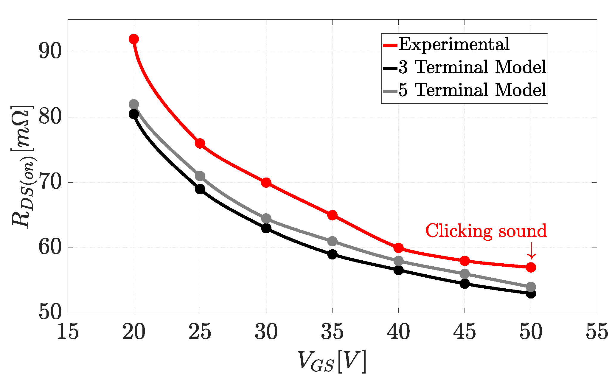
| 20 | 92 | - | 80.5 | −12.5 | 82 | −10.87 |
| 25 | 76 | −17.4 | 69 | −9.2 | 71 | −6.58 |
| 30 | 70 | −29.0 | 63 | −10 | 64.5 | −7.86 |
| 35 | 65 | −38.6 | 59 | −9.2 | 61 | −6.15 |
| 40 | 60 | −49.2 | 56.6 | −5.67 | 58 | −3.33 |
| 45 | 58 | −56.7 | 54.5 | −6.03 | 56 | −3.45 |
| 50 | 57 | −60.3 | 53 | −7.02 | 54 | −5.26 |
| (V) | (V) | Conduction Losses (W) | % Reduction w.r.t Losses at V |
|---|---|---|---|
| 20 | 1.84 | 36.8 | − |
| 25 | 1.52 | 30.4 | −17.4 |
| 30 | 1.4 | 28 | −23.9 |
| 35 | 1.3 | 26 | −29.4 |
| 40 | 1.2 | 24 | −34.8 |
| 45 | 1.16 | 23.2 | −37.0 |
| 50 | 1.14 | 22.8 | −38.0 |
| Methods | ||||
|---|---|---|---|---|
| 3-Terminal Model | 5-Terminal Model | |||
| (V) | (m) | (in %) w.r.t at V | (m) | Deviation from Experiments (in %) |
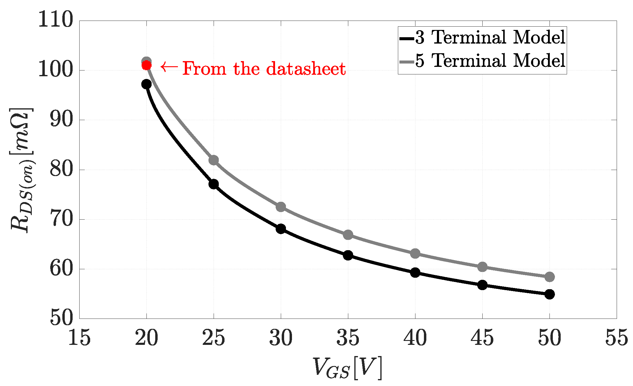
| 20 | 97.02 | - | 101.73 | - |
| 25 | 77.11 | −20.67 | 81.92 | −19.5 |
| 30 | 68.11 | −29.93 | 72.52 | −28.7 |
| 35 | 62.78 | −35.41 | 66.990 | −34.2 |
| 40 | 59.30 | −38.99 | 63.14 | −37.9 |
| 45 | 56.81 | −41.56 | 60.45 | −40.6 |
| 50 | 54.94 | −43.48 | 58.4387 | −42.6 |
Disclaimer/Publisher’s Note: The statements, opinions and data contained in all publications are solely those of the individual author(s) and contributor(s) and not of MDPI and/or the editor(s). MDPI and/or the editor(s) disclaim responsibility for any injury to people or property resulting from any ideas, methods, instructions or products referred to in the content. |
© 2024 by the authors. Licensee MDPI, Basel, Switzerland. This article is an open access article distributed under the terms and conditions of the Creative Commons Attribution (CC BY) license (https://creativecommons.org/licenses/by/4.0/).
Share and Cite
Bhadoria, S.; Xu, Q.; Wang, X.; Nee, H.-P. Concept of Enabling Over-Current Capability of Silicon-Carbide-Based Power Converters with Gate Voltage Augmentation. Energies 2024, 17, 4319. https://doi.org/10.3390/en17174319
Bhadoria S, Xu Q, Wang X, Nee H-P. Concept of Enabling Over-Current Capability of Silicon-Carbide-Based Power Converters with Gate Voltage Augmentation. Energies. 2024; 17(17):4319. https://doi.org/10.3390/en17174319
Chicago/Turabian StyleBhadoria, Shubhangi, Qianwen Xu, Xiongfei Wang, and Hans-Peter Nee. 2024. "Concept of Enabling Over-Current Capability of Silicon-Carbide-Based Power Converters with Gate Voltage Augmentation" Energies 17, no. 17: 4319. https://doi.org/10.3390/en17174319
APA StyleBhadoria, S., Xu, Q., Wang, X., & Nee, H.-P. (2024). Concept of Enabling Over-Current Capability of Silicon-Carbide-Based Power Converters with Gate Voltage Augmentation. Energies, 17(17), 4319. https://doi.org/10.3390/en17174319