Review

Mechanical Characterization of Sintered Silver Materials for Power Device Packaging: A Review

by
Keisuke Wakamoto
1,* and
Takahiro Namazu
2
1
Research and Development Center, ROHM Co., Ltd., Kyoto 615-8585, Japan
2
Faculty of Engineering, Uzumasa, Kyoto University of Advanced Science, Kyoto 615-8577, Japan
*
Author to whom correspondence should be addressed.
Energies 2024, 17(16), 4105; https://doi.org/10.3390/en17164105
Submission received: 17 July 2024 / Revised: 9 August 2024 / Accepted: 16 August 2024 / Published: 18 August 2024
(This article belongs to the Section F: Electrical Engineering)

Abstract

:
This paper reviews sintered silver (s-Ag) die-attach materials for wide band gap (WBG) semiconductor packaging. WBG devices that die-attach with s-Ag have attracted a lot of attention owing to their low energy loss and high temperature operation capabilities. For their practical operation, a reliability design should be established based on the failure of physics of the s-Ag die layer. This paper first focuses on the material characteristics of the s-Ag and tensile mechanical properties. Then, the s-Ag die-attach reliability is assessed with high-temperature storage, power cycling, and thermal shock tests. Each fracture mode was discussed by considering both the fracture surface analysis results and its mechanical properties. Finally, the effective reliability design parameters of the s-Ag die layer are introduced.

1. Introduction

Carbon dioxide (CO2) emissions are a common issue affecting global warming. To reduce CO2 emissions, it is industrially indispensable to reduce energy translation systems powered by fossil fuels, such as internal combustion engines in vehicles. The number of electric vehicles (EVs) powered by electricity has gradually increased because EVs generate no CO2 emissions while running. EVs consist of an electricity power control system that can regulate the voltage by switching the semiconductor devices, enhancing the efficiency of the motor operation. Silicon (Si) semiconductor devices have been generally adopted as switching devices. However, the power conversion efficiency has theoretical performance limitations [1]. Wide band gap (WBG) devices made of silicon carbide (SiC) and gallium nitride (GaN) have been developed as new candidate devices to further improve the power conversion efficiency. Previous studies have reported that WBG devices can achieve low power loss under a high-speed switching frequency owing to their higher saturation electron drift velocity value compared to those with Si [2,3]. In addition, since the WBG’s value is high compared to the value of Si, WBG devices can operate at over 300 °C [4]. Accordingly, many researchers have expected that new power control units with WBG devices can break the conventional power density of units with Si.
New thermal management is crucially important to extract WBG device properties for application in packaging products. As the WBG device’s size decreases, the increase in device thermal density can give rise to the decisive failure of products with the progressing degradation of the die material. Then, the heat generated from WBG devices must immediately diffuse to spread in the metal substrate through the die material. For example, double-side cooling packaging technology has developed so that two direct bonded copper (DBC) substrates are bonded on both device faces to expand the cooling area [5,6]. For single-side cooling, a thick copper lead frame substrate has been adopted to efficiently expand the heat flux in the substrate [7,8]. As for the representative achievement, Fuji Electric Company released a full SiC inverter with air cooling with 40 kW/L in 2012. This power density value of SiC inverters breaks, which is about two times higher than the value in the Si inverter power [9]. For previous packaging [5,6,7,8,9], the die material employed solder that was bonded to form an alloy with another metal (Cu, Ni, etc.) in a liquid phase. However, the solder’s physical properties are reaching their physical limitation. The thermal conductivity and melting point are restricted to 60 W/mK and 300 °C, respectively [10]. Therefore, solder can no longer survive in future packaging with high-power density. A new die-attach technology should be developed to break the conventional solder’s physical limitations.
As an alternative to soldering, sintered silver (s-Ag) die-attach technology was developed from the late 1980s [11,12,13,14]. Unlike soldering, s-Ag can be bonded through Ag atomic diffusion, driven by the external energy of an applied press and temperature under the solid state. As a primary feature, since the s-Ag surface energy is remarkably high owing to its composition of micro-/nanoscale Ag particles, the s-Ag can be bonded with low energy [15]. For example, nano-Ag particles start to form a necking at the grain boundary from 175 °C [16]. After bonding, the structure is porous and is located at the grain boundary, which hinders thermal conduction in the die layer. However, the thermal conductivity of porous s-Ag exceeds 200 W/mK, which is about three times higher than the value of solder [17,18,19,20]. In addition, s-Ag’s melting point equals the bulk Ag with 961 °C. Consequently, s-Ag is one of the most promising SiC die-attach candidates.
For practical application products, fabricated products are essential to satisfy Lv324 standards, reflecting on actual operation mode [21]. Above all, the die-attach layers are commonly subjected to thermal and mechanical stresses caused mainly by differences in thermal expansion coefficients between the application elements. Power cycling tests (PCTs) have commonly been adopted as reliability tests, reflecting the power dissipation cycling of the device while switching operations [22]. During a PCT, the electrical load is applied to the device and the highest temperature swings between RT and 175 °C within a few seconds. Since the temperature holding time in the PCT is equal to zero, the device’s heat is not completely spread, creating the highest temperature spot area in the device. This local temperature variation gives rise to the die degradation surrounding this area during the PCT. Thermal shock tests (TSTs) that fluctuate the temperature of the atmosphere have also been majorly adopted to assess the durability of die-attach materials [23]. Notably, WBG device materials such as SiC have a large Young’s modulus, the value of which is about three times larger than the value of Si. This primary feature enhances the applied stress in the SiC die layer during reliability tests such as TSTs and PCTs, accelerating the die delamination.
This deteriorated die layer, after reliability tests, shrinks the thermal pass through the die layer, which accelerates the packaging failure by increasing the local heat flux around the die layer. To quantitively elucidate the degradation of the die layer, we should assess the product’s thermal resistance (Rth), defined as the temperature difference between the highest temperature at the chip and the ambient temperature divided by the power loss at the chip. Since the Rth value is sensitively affected by the die layer’s thickness and porous distribution, a transient thermal impedance methodology has been commonly adopted to elucidate the state of bonding [24]. In general, the Rth increasing rate (rth), which is defined as the increase in the Rth value after reliability tests divided by the initial Rth has been set to 20% as a product lifetime [21]. The horizontal crack in the die layer crucially increased rth by hindering the heat path from the chip towards the bottom layers through the die layer [25]. As a primary step for designing the lifetime of products, the control scheme of the s-Ag deterioration during reliability tests should be correctly established, so an SiC die attach with s-Ag packaging will be safe and have long-term durability during practical operation.
This review article focuses on the s-Ag degradation mechanism based on micro- and macroscopic experimental and calculation results. Firstly, the s-Ag bonding mechanism is introduced to provide a basic understanding of s-Ag. Then, representative Ag paste types and their specifications are summarized. The microstructure with the pore and grain is reviewed to identify the relationship between the sintering condition and the s-Ag microstructure. After that, the tensile mechanical properties of s-Ag films are introduced to quantify the evaluation of s-Ag durability during TSTs. The fracture characteristics of s-Ag are also reviewed based on the fracture surface observations after tensile tests. In addition, in situ scanning electron microscopy (SEM) tensile test results are introduced to give an insight into the s-Ag grain and pore degradation and the ductile deformation mechanism at high temperatures. Next, the topic shifts from monolithic s-Ag properties to the s-Ag die-attach assembly’s reliability. Microstructure evolution results after high-temperature storage (HTS) tests are introduced to clarify the thermal effect on the s-Ag microstructure aging. Then, the s-Ag die layer failure mode after a PCT is reviewed. The main failure cause of the PCT will be discussed. Finally, the s-Ag die layer failure mode observations after TSTs are reviewed to consider the central failure cause during the TST. The essential guidance for reducing degradation is stated from the viewpoint of the assembling structure and s-Ag microstructure. After that, the quantitive s-Ag die layer degradation assessments are introduced. Since only calculation results lack information on the s-Ag durability itself. Thus, a damage parameter (DP) is newly introduced in this review, which is defined as the accumulated plastic von Mises strain (APS) is calculated by the finite element analysis (FEA) divided by the plastic strain obtained from a stress–strain (S–S) curve by uniaxial tensile testing. The DP effectiveness for s-Ag die delamination is verified by comparing the mechanical bending tests and TSTs results. Finally, the authors make conclusions about the s-Ag die layer degradation mechanism with a TST.

2. Sintered Silver Material Characteristics

2.1. Sintering Process

First, let us focus on the s-Ag die-attach conventional process step, as shown in Figure 1. The paste, including the Ag particles coated with organic stabilizer, is stencil printed on the substrate. Then, the organic solvent is dried by preheating to prevent any squeeze out of the Ag paste. Notably, excessive preheating gives rise to the hardening of the paste, which forms pores and cracks in the dried film after the preheating [26]. Therefore, we optimized the preheating process time and temperature to fit the individual paste characteristics. Thermogravimetric analysis of the paste’s weight and time relations informed us about the optimized preheating temperature. When the paste weight loss drastically drops at a specific temperature, the condition is considered suitable for the preheating temperature [27]. In addition, the appropriate heat time can be determined by taking a surface observation as a function of the heating time at an appropriate temperature. When the paste color completely fades from the paste color without voids, we can judge that this preheating time is appropriate [28]. Finally, the external press and temperature are given by uniaxial stage motion powered by a servo hydraulic in the sintering process. This breaks the organic stabilizer to expose the raw Ag surface for interdiffusion efficiently. To adjust the slight height difference between the stage and chip top surface, a cushion material such as a Teflon sheet or carbon sheet is placed on the chip, as shown in the right illustration of Figure 1. The commercial tester of this sintering is produced with an oven or press suppliers such as ASM Technology (Bangalore, India), Boschman Technologies (Duiven, The Netherlands), Locatelli Meccanica (Subbiano, Italy), and PINK GmbH Thermosysteme (Wertheim, Germany). It is worth noting that pores are inevitably formed to make gas pathways outside during the sintering process [29,30]. For s-Ag bonding, homogeneous elements of the Ag surface are used by electroplating, electroless plating, and sputtering, all of which are primarily able to ensure an excellent qualification between the porous s-Ag and the dense Ag [31,32,33]. Sintering is preferable to make a robust bonding interface between the metal surfaces, even though a low temperature and pressure are applied. Based on Herring’s scaling laws, the sintering driving force is expressed in [34]
d ρ d t = D r i v i n g   f o r c e × M o b i l i t y = A γ 3 r × D c k B T
where ρ is the relative density, A is the constant, γ is the free surface energy of the Ag particle, r is the average particle size, Dc is the atomic diffusivity, kB is the Boltzmann’s constant, and T is the absolute temperature. Reducing the Ag particle’s size and increasing the temperature or pressure can significantly improve the driving force and mobility, respectively, leading to efficient sintering of the Ag particles.
As for the classification of Ag particles, three types have been developed, as shown in Figure 2 [35]. Nano-Ag particles provide low-temperature sintering under a slight applied pressure owing to the top sintering driving force among the three types of Ag particles. In the mid-2000’s, Bai J. G. et al. [36] reported that nano-Ag could be sintered at 280 °C without applied pressure. Nano-Ag sintering has recently been achieved at 175 °C [16]. The storage of nano-Ag is strictly required to prevent self-aggregation. Thus, high molecules of an organic binder should be coated around the Ag particles to generate high electric repulsive force between the nano-Ag particles. As a result, a lengthy dry procedure is inevitable, which increases the process cost [37,38]. For micro-Ag particles, since the total surface energy is low compared to nano-Ag, the driving force of the sintering is low. However, the Heraeus company originally developed apaste (ASP 338-28) which can be sintered at a considerable sintering condition (e.g., 10 MPa pressure at 250 °C) [39]. A mixture of micro-Ag flakes and submicron Ag particles, called a “hybrid paste”, has been developed to maintain low production costs and high sintering driving forces [35,40,41,42]. The micro-Ag flakes fulfill the role of a skeleton, and the submicron Ag particles fill gaps between the micro flakes to reduce the space in the sintered layer. Apart from the Ag particle’s free energy, redox reaction energy can accelerate the mobility of Ag. For example, Hirose A. et al. [43] developed Ag metal–organic nano-Ag particles, which are produced by the reduction of Ag2O particles. The reduction reaction speed of Ag2O was found to be accelerated by adding reducing organic solvents such as diethylene glycol, which can complete this reduction at around 160 °C. In addition, Ag nanoparticles smaller than 10 nm are generated to adhere on the surface as a result of this thermal decomposition reaction [44]. This nanoparticle generation is similar to the formation of Ag or Cu nanoparticles from bulk Ag or Cu in the presence of water and oxygen under reduction circumstances [45,46]. Once the Ag nanoparticles are obtained, a high surface to volume ratio can depress the Ag melting point, making the Ag diffusivity more reactive [47]. As a result, this redox paste can achieve a low temperature and pressure bonding. This unique material is challenging to bond with other materials, such as aluminum and silicon-based materials [48,49,50,51,52].

2.2. Microstructure Characterization

To characterize the microstructure of the porous and grain in the s-Ag layer, precise pretreatments to make a smooth surface are crucial before taking observations. The observation sample is cross cut by a blade dicing machine. Then, the sample is encapsulated with a resin block. After that, the specimen is polished with abrasive paper in the water base suspensions. A monocrystalline diamond slurry solution then performs the buffing polish. Finally, the ion milling process is treated to planarize the sample surface. After that, this planarized surface is analyzed by SEM to determine the pore and grain boundary, and electron backscatter diffraction (EBSD) is used for crystal orientation, local dislocation, and grain boundary angle etc. The obtained data are transferred to binary images, which are identified with image software (Image J 1.54j 12, National Institute of Health, Bethesda, MD, USA or Wafermasters, Dublin, CA, USA). This software gives us binarized geometrical information quantitatively. For instance, porosity, neck length, grain size, and grain number are extracted from the obtained two-dimensional (2D) cross-sectional SEM images [53,54]. In addition, three-dimensional (3D) image analysis is performed by stacking 2D SEM observation images treated with focused ion beam (FIB) milling. A new fresh surface from the FIM milling is repeatedly captured by SEM. Then, these images are stacked to form a volume microstructure information [55,56]. Since this inspection methodology is a destructive, Zabihzadeh S. et al. obtained 3D s-Ag images with high-resolution ptychographic X-ray computed tomography as a nondestructive inspection [57]. These 3D images are utilized for the construction of 3D FEA models, which investigate the local stress distribution surrounding the pore [58]. From the results of the comparison between the 2D and 3D images of s-Ag, the obtained microstructure parameter of s-Ag matched well [18]. Accordingly, 2D observation is conventionally adopted as the s-Ag microstructure inspection methodology.
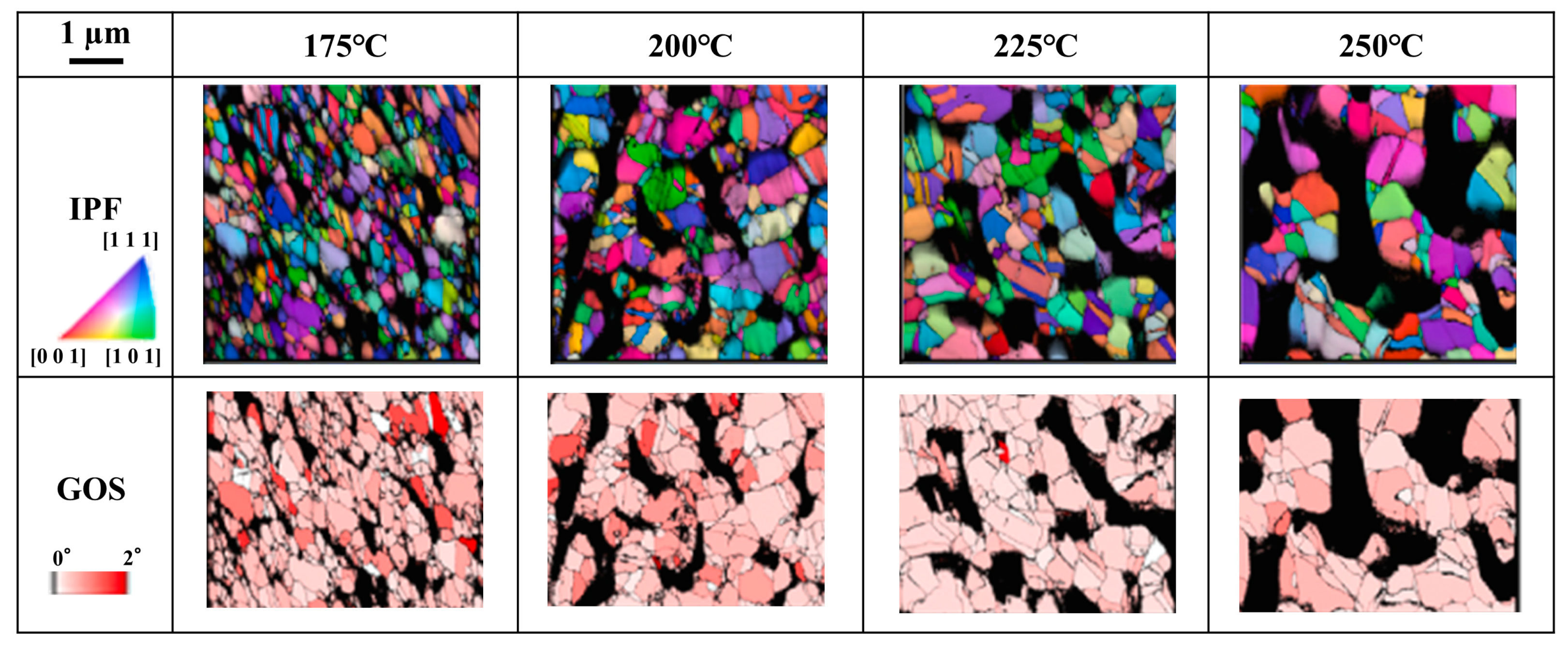
Then, let us focus on the results of the representative 2D microstructure analysis of the s-Ag microstructures. Figure 3 shows the EBSD analysis results of the submicron-Ag sintered structures as a function of sintering temperatures from 175 to 250 °C under no applied pressure for 10 min [59]. The upper side and downside images are indicative of the inverse pole figure (IPF) images and grain orientation spread (GOS) images. IPF refers to the crystal orientation direction distributions. GOS refers to the average value of the orientation spread in the grain, evaluating the degree of recrystallization in s-Ag. In the IPF images, the crystal orientation is random, irrespective of sintering temperature, indicating that s-Ag is a polycrystalline material. In addition, the necking length between grains grows with the increase in sintering temperature. That is, bonding temperature was a decisive factor for increasing the interfacial connection. In the GOS images, the GOS value tends to decrease with temperature increases. The high GOS value with a red area almost disappears between 200 and 225 °C, indicating that the recrystallization temperature of s-Ag is around this temperature. Next, we show the applied sinter pressure dependence on the s-Ag microstructure through our previous study.
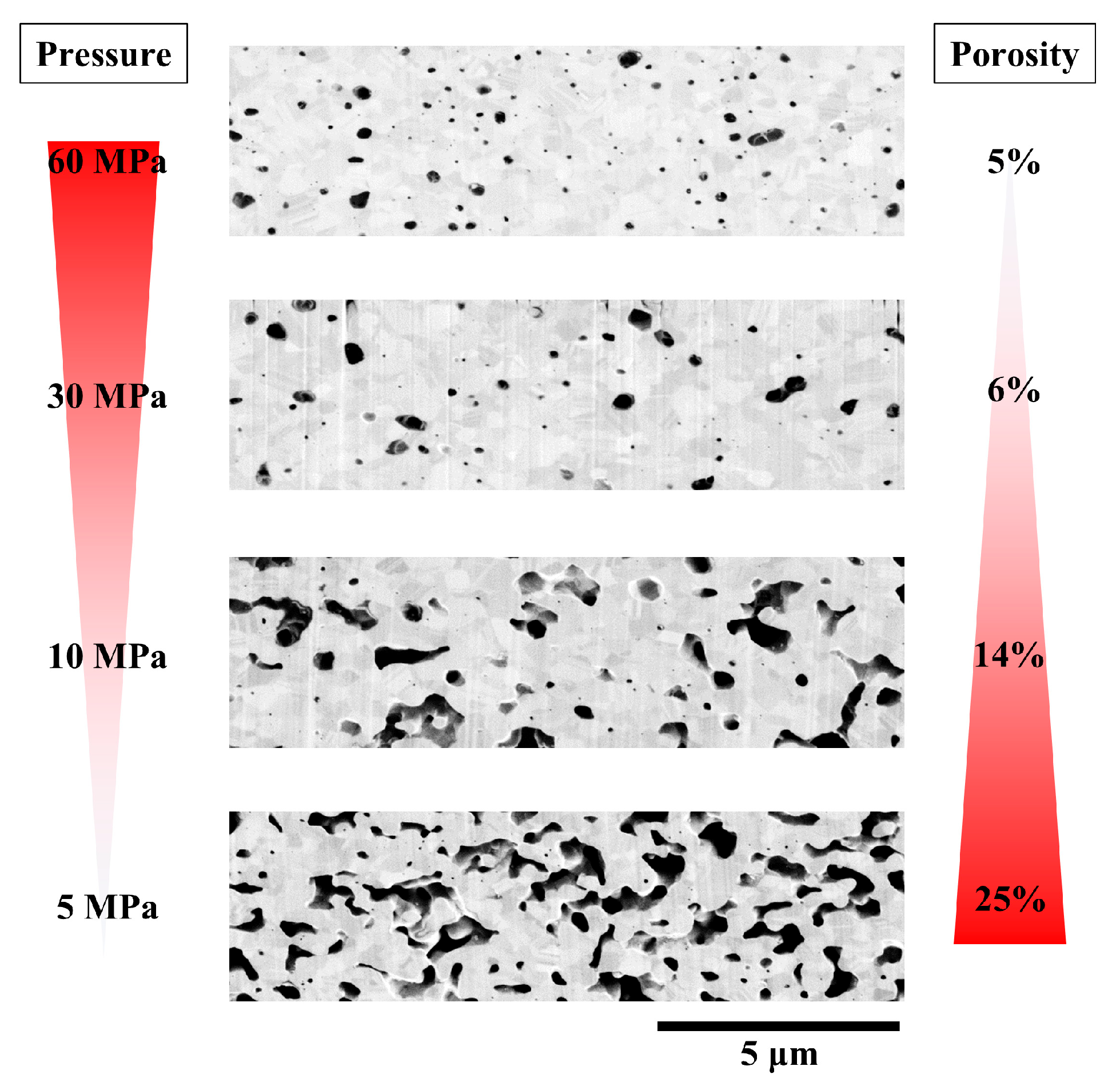
Figure 4 shows a cross-section fo the SEM observation results of the nano-Ag sintered structures depending on the applied pressure from 5 to 60 MPa under 300 °C for 10 min [53]. The s-Ag porosity, calculated as the ratio of the pore area to the observed cross-sectional area, is also described on the right side of each photograph. As a pivotal feature, the applied pressure strongly affects the formation of pores in the layer. Under a slight pressure of 5 and 10 MPa, the pore shape is irregular, similarly to the peanut shape, which is locally located close to each other. With an increased applied pressure above 30 MPa, the pore shape changes to an almost spherical shape, located discretely in the layer. The porosity value decreases from 25% at 5 MPa pressure to 14% at 10 MPa pressure. Then, the porosity saturates at around 5% at 30 and 60 MPa pressure. Applied pressure worked well to reduce the porosity in the s-Ag layer. In the next subsection, the porosity influences on s-Ag mechanical properties will be reviewed.

2.3. Tensile Mechanical Properties

It is necessary to investigate the mechanical properties of s-Ag to reflect the obtained results on the s-Ag die layer’s reliability. Tensile tests are generally implemented to derive a material’s mechanical properties directly from S–S diagrams. The S–S curves provide us with the material mechanical parameter of Young’s modulus (E), the ultimate tensile strength (UTS), and the breaking strain (BS). Here, a universal tensile test methodology is introduced. For tensile tests, a dog bone-shaped specimen is commonly used to limit a stress intensity area to the middle section of the specimen. To date, the Ag paste has been directly screen printed by a patterned mask, which was sintered to form a dog bone specimen [60,61], and s-Ag film has been cut with machining tools to form a dog bone specimen [53]. During the tensile tests, the specimen is pulled by a static stage motion until the specimen breaks. The applied force is measured by the load cell, and the specimen elongation is directly measured by the CCD camera, which is placed above the specimen to perform image analysis with the imaging software. Finally, the measured force and elongation in the specimen translate into the stress and strain relationships. These standard tensile test specimen scale dimensions are on a mm scale with a specimen footprint 50~300 μm thick.
To further downsize the tensile tests, Namazu. T et al. developed the original tester to hook a thin film specimen using a rectangular pin and square hole [62,63,64]. The test element consists of a thin film specimen less than 10 μm, two squared holes, and four springs surrounding the moving part made from Si. The film length and width of the specimen were 200~500 μm and 20~50 μm, respectively. The Si frame is micromachined by deep reactive ion etching. Only a thin film section is self-standing, whereas other sections have double thin film and Si frame layers. Tests are implemented twice to obtain S–S curves of the films. First, the measured force is both the Si frame and the film specimen. After the rupture of the film specimen, a second test is implemented. In this test, the tension only applies to the Si frame. Therefore, the film specimen of the S–S curves can be obtained by subtracting from the first S–S curves to the second S–S curves. Since this original tester size is compact, a combination of analyses can also be achieved. X-ray diffraction analysis or Raman spectroscopy analysis can be simultaneously obtained during tensile tests to clarify microstructural changes in crystallinity or stress mapping [62,63,65,66].
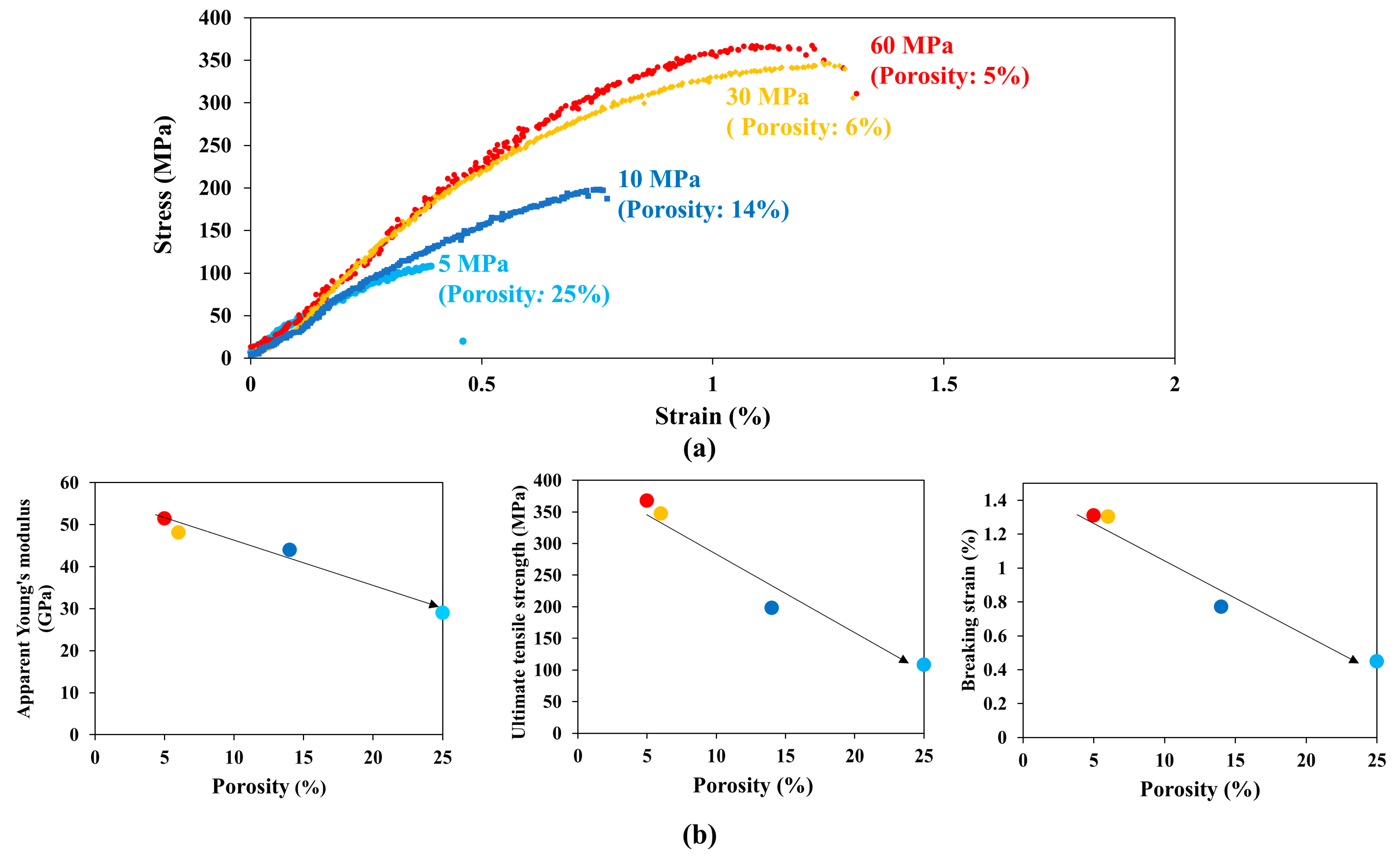
Then, let us focus on the representative S–S curves of the s-Ag specimen, as introduced in Figure 4, to understand their pore dependences on the mechanical properties [53]. As seen from the S–S curves at RT in Figure 5a, all specimens fractured in a brittle manner even though the porosity has a small value of 5%. All S–S curves show an almost linear trend of the specimen immediately fracturing after it reached the highest value in the curve. This trend differs from the bulk Ag characteristic of nonlinear S–S curves [67], showing a ductile fracture manner. The existence of the pore in the s-Ag would make a difference to the bulk Ag without porosity. The strength of the s-Ag specimens depends on porosity, indicating that smaller porosity with higher applied pressure strengthens the durability of the evaluated s-Ag specimen. Figure 5b shows the mechanical properties of E, UTS, and BS as a function of porosity, extracted from the obtained S–S curves. All parameters negatively correlate with porosity, as was also reported in other studies [68,69,70]. That is, including the pore largely result in toral deformation, which decreased the E of the s-Ag. However, local stress concentrates around pores, which accelerate the s-Ag specimen’s fracture and decrease the UTS and BS [71]. Therefore, it can be concluded that the minute porosity at around 5% in s-Ag can provide better durability against the applied stress. Next, the temperature dependence on this small porosity s-Ag’s tensile properties is introduced to understand the s-Ag S–S curves’ characteristics under the practical use of temperature.
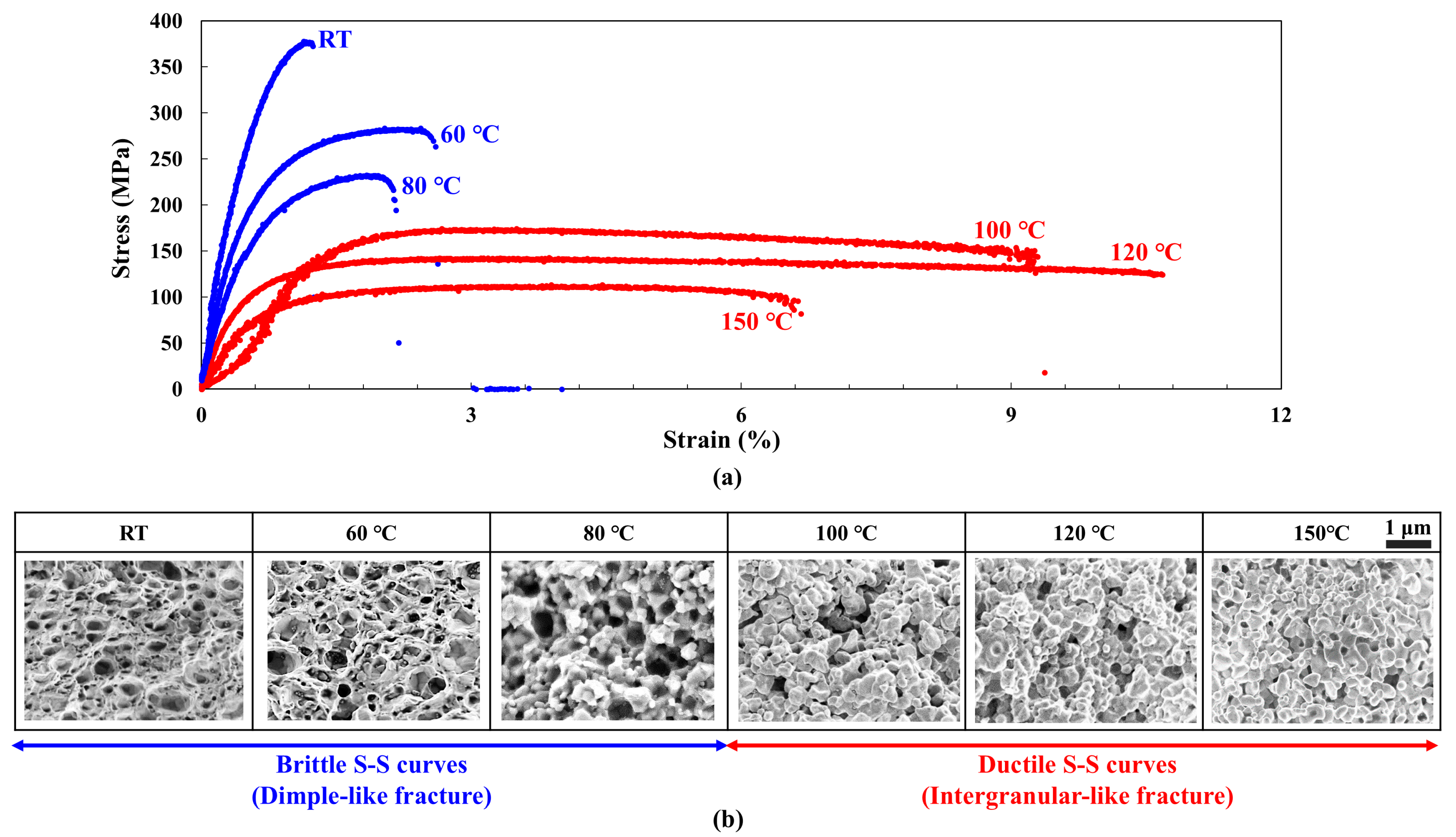
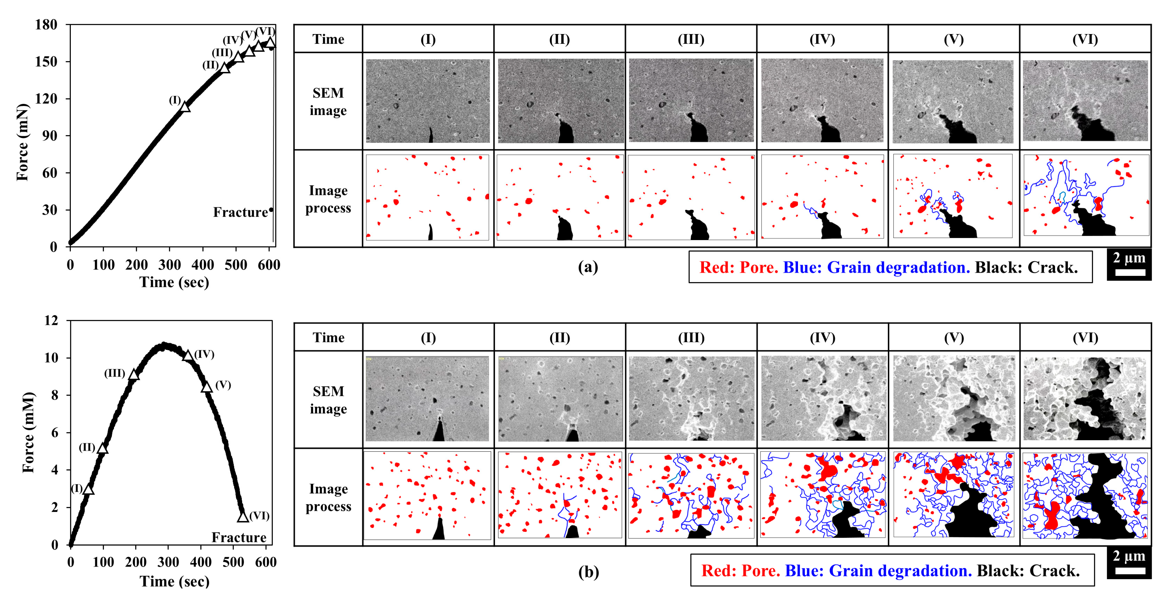
Figure 6 shows a nano-s-Ag sintered film specimen with 5% porosity from RT to 150 °C and their fracture surface observations with SEM [72,73]. Red and blue plots in the S–S curves indicate the brittle and ductile curves, respectively. The brittle and ductile threshold is defined as the 1.5% strain difference between the yield strength’s strain and the fracture’s strain. The S–S curves show brittle curves from RT to 80 °C, whereas the other S–S curves show ductile curves from 100 to 150 °C. All S–S curves show wide plastic strain exceeding 5% at these temperatures. This plateau range expansion with increased temperature was also confirmed irrespective of the porosity in the s-Ag [74,75,76]. The s-Ag’s brittle to ductile transition temperature was between 80 to 100 °C. In addition, as shown in Figure 6b, many convex structures with S–S curves were utterly revealed by local in situ SEM uniaxial tensile tests with 8 × 5 μm2 at the crack tips [77]. Figure 7a,b show the in situ SEM uniaxial tensile test results at RT and 300 °C, respectively. The graphs on the left side show the relationship between the applied force and the time of the evaluated s-Ag specimens. The right-side snapshots were taken during the experiments, and the timing corresponds to the index as a Greek number in the left-side graphs. At RT, the specimen fractured at the maximum force immediately. In the SEM snapshots around a pre-crack, the microstructure of the pore was not significantly grown during tests. A local grain boundary degradation can be seen around the tip of the crack. In contrast, at 300 °C, the force and time relationships clearly show a nonlinear trend. After reaching the maximum force, the force gradually decreases until the specimen is fractured. The microstructure of s-Ag pores was gradually grown with the grain boundary degradation from the initial to the fractured state.
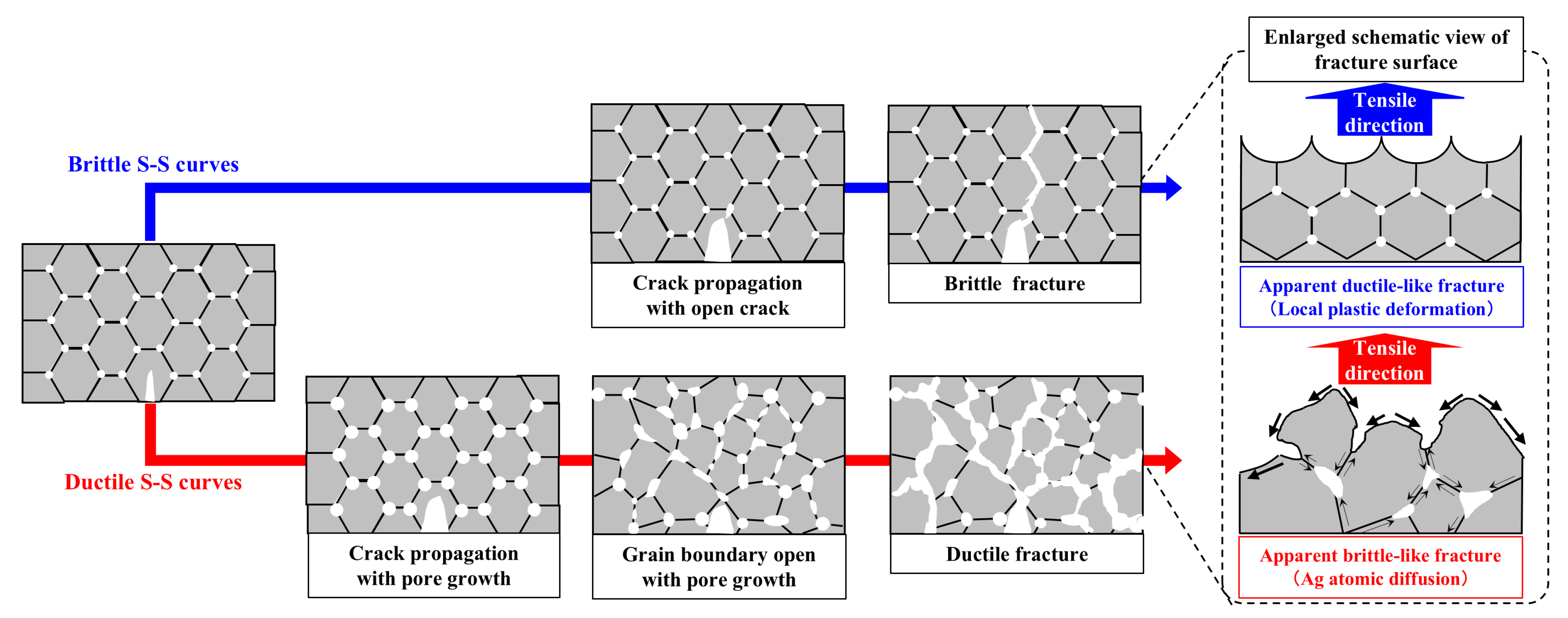
Considering the obtained experiment results, the fracture characteristic of s-Ag is described in Figure 8. At RT, with brittle S–S curves, a stress is locally concentrated at the tip of the crack, which then propagated along the grain boundary to immediately become a failure. In the microscopic view, a slight plastic deformation happened which made a fracture surface with dimples, causing an apparent ductile-like fracture. On the contrary, at high temperatures with ductile S–S curves, s-Ag failure gradually progressed. This fracture characteristic difference can be explained by considering the Ag atom gliding speed at the grain boundary. The Ag atom gliding speed in following equation was proposed by Ashby M. F. in 1972 [78],
d γ d t = 8 b β τ D b k T
where b is the burgers vector, β is the boundary thickness, τ is the applied stress, k is the Boltzmann’s constant, T is the absolute temperature, and Db is the boundary diffusion coefficient, which is derived as
D b = D 0 e x p E a k T
where D0 is the pre-exponential constant for grain boundary diffusion [79]. Ea is the activation energy for the grain boundary [80]. Each input value can be referred to in the previous study. From these calculations, it was found that /dt can be described as a function of τ and Db/T. The temperature dependence on /dt is much higher than on the τ. Accordingly, the temperature is a key factor for determining the value of /dt. In addition, the /dt value determines the ductile and brittle S–S curves of s-Ag considering the previous S–S curve results [61,68,72,73,81]. The threshold value was derived with the following:
d γ d t τ , D b T = 16 ( μ m / s e c )

3. Sintered Silver Die-Attach Reliability

3.1. High Temperature Storage Test

In this section, the topic shifts from s-Ag monolithic film properties for die-attach layer degradation assessments toward the actual product’s reliability design exposed by thermal and mechanical stress. For the preparation of die-attached assemblies, the process step is identical to those in Figure 1. In this subsection, the microstructure changes in s-Ag are reviewed through a HTS to understand the thermal stability of the die layer. Figure 9 shows the representative cross-sectional SEM images of the nano-type s-Ag die layer during the HTS at 150 °C for 500 h. Comparing the before and after HTSs in the SEM images, the porous structure is significantly coarsened after HTS. Of course, the pore growth was known to be accelerated by increasing the HTS temperature [82]. Since the effective bonding area shrinks under pore growth, the adhesive strength between the s-Ag layer and the substrate surface is weakened by performing shear mechanical force tests [83,84]. Note that, if external mechanical stress is not applied to the die layer like it is during HTS, the s-Ag die layer shows no delamination [85]. Several techniques have already been proposed to maintain s-Ag’s porous structures during HTS. Mannan S. H. et al. reported that the oxidized s-Ag pore surface could prevent Ag grain diffusion for maintaining the microstructure during HTS owing to its thermostable structure [86,87]. The oxidized s-Ag pore surface can be easily formed by dipping in RT water for 10 min after sintering. From the material side, adding SiC particles suppresses Ag diffusion at the grain boundary [88,89]. Moreover, diamond particle addition to Ag paste also positively affected the suppression of Ag pore growth [90]. However, there is a report that says adding copper oxide particles restricts Ag diffusion at high temperatures, which sacrifices the ductility of s-Ag even it strengthens the s-Ag [91]. To design a reliabile s-Ag layer, a “high strength material” or “high ductility material” should be considered carefully based on the experiment and calculation results. This topic will be discussed later in Chapter 4.

3.2. Power Cycling Test

In this section, the s-Ag die layer’s failure mode is mainly reviewed by PCT. As introduced in the initial section, PCTs reflect on the switching motion of devices in a practical application. The highest temperature in the chip generally varies from RT to 175 °C within several seconds by applying a current to the chip. As a result, the temperature distribution in the chip is concentric around the highest current density area [22,92,93]. The fracture area in the die area has been known to be associated with this heat spot area [94]. The stress distribution can be assessed through FEA, considering this temperature distribution as a boundary condition. The stress level at the s-Ag die layer during the PCT showed an elastic region [92,93]. In addition, the travel time between the lowest and highest temperatures in a PCT is about 100 times shorter than that of a TST. Given this strain level and PCT travel time, the induced strain speed of the s-Ag die layer during the PCT is considered to be much higher than the strain speed in the TST [85]. The s-Ag tensile property is known to change a brittle material at 150 °C under the strain speed order of 10−2 [68]. That is, the s-Ag die layer is considered to show a brittle characteristic during the PCT [95]. Then, we demonstrate the representative failure mode in the s-Ag die layer after the PCT through Figure 10 [25]. This cross-sectional SEM image was taken after 116,358 cycles of PCTs, and s-Ag’s initial porosity was about 2%. As can be seen in the photograph of Figure 10, almost all cracks progressed in a horizontal direction from the bottom of the chip to the top surface of the substrate. Since the brittle material’s crack progresses perpendicular to the tensile principal stress, this vertical crack is ascribed to the horizontal tensile principal stress in the s-Ag die layer. Notably, this vertical crack did not result in an increase of the rth value. Therefore, it can be concluded that this kind of vertical crack is favorable for maintaining the heat dissipation characteristics of packaging products. In the next subsection, we discuss another s-Ag die layer fracture mode caused by the TST.

3.3. Thermal Shock Test

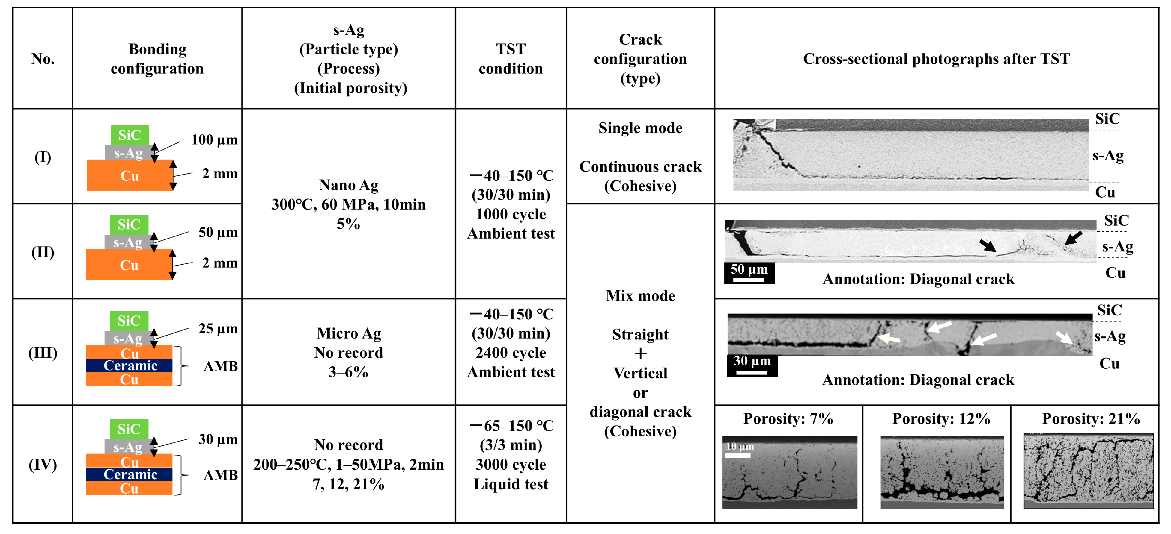
Since the packaging includes dissimilar materials bonded with each other, it generates a thermal warpage around a bonded section by repeated temperature variation tests in TSTs [96,97]. The repeated warpage causes “mechanical stress” in the die layer. Then, the delamination proceeds from the corner of the s-Ag die layer which concentrates the stress in the s-Ag layer [98,99]. The representative travel time between the lowest and highest temperature is about the min order, for which the strain speed at the s-Ag die layer is around 10−4 when associated with quasistatic speed of tensile tests, as shown in Figure 6 [77]. Therefore, the s-Ag deformed in plasticity at higher temperatures in the TSTs. In addition, high-temperature exposure deteriorates the die layer with “thermal stress” during TSTs. Therefore, TSTs assess the effects of mechanical and thermal stress on the s-Ag layer. Figure 11 shows the representative die layer cross-sectional observation results summarized from previous studies [85,100,101]. The crack modes after TSTs are roughly divided into “single mode” and “mix mode” groups and compares the characteristics of the two groups.
First, the single mode with straight continuous cracking is introduced here. As a feature for (I), the crack starts at the corner of the edge and propagates to the inside at an inclined angle. The incline of this crack changes to a horizontal crack, which progresses along the substrate surface, as is shown in the top right cross-sectional SEM image. This primary fracture mode is mainly given rise to by mechanical stress, which is well imitated by mechanical bending tests under the shear force diagram mode [99,102,103,104]. It was confirmed that the crack direction was associated with the maximum shear stress direction at the crack’s tip [103]. In addition, the crack speed per cycle can be controlled by modifying the mechanical bending test conditions to fit the crack speed during the TST [99]. Notably, substrate materials such as stainless-steel alloys and Ti-6Al-4V alloys are recommended for use in high stress yield material to allow bending deformation without plastic deformation during bending tests [99,102,104]. The critical parameters for fitting the crack speed of mechanical bending tests to that of a TST were test temperature and strain rate in the s-Ag layer, not the exposure time to high temperatures.
The “mix mode” was also observed in (II), (III), and (IV) of Figure 11. Another risk is the formation of a discontinuous crack with a vertical or diagonal direction, differing from the continuous horizontal straight crack. Here we review the causes of each state from (II) to (IV). For (II), the difference from (I) is the s-Ag die layer thickness, since the s-Ag die layer thickness in (II) is half of the thickness in the s-Ag die layer. Therefore, higher stress would be caused by lower stiffness of the die layer during the TST in (II) [98,105]. The continuous straight crack changes to a discontinuous crack from the middle. In addition, local pore growth can be seen around the discontinuous crack. This pore growth matches the thermal aging phenomena, as introduced in Section 3.1. Therefore, increased stress in the die layer accelerates thermal aging phenomena in comparison with those in (I) [106,107]. For (III), the difference from (I) is the substrate structure from bare Cu to the active metal brazed (AMB) substrate and the s-Ag die layer thickness. In addition, the observed photograph was taken after 2400 cycles of TSTs, not 1000 cycles of TSTs. Since the essential AMB stiffness is much lower than the stiffness of a bare thick Cu substrate, then the stress to the die layer tends to be low in the s-Ag die layer [108,109]. However, the discontinuous crack was also seen in the die layer, as depicted in the photograph with an area of white annotation. Notably, the Cu substrate surface shows a hill and valley structure. In general, AMB substrate was fabricated at 800–1000 °C, and the crystal size of Cu is sub-millimeter order, which is more than ten times larger than the Cu substrate without this high thermal treatment at least [110]. According to the Hall–Petch relation [111], the strength of the material becomes low due to the ease of dislocation motion in the large Cu grain used in the AMB. For Cu, the strength value decreases to 1/10 of the value when increasing the crystal size ten times. Consequently, AMB Cu is easily yielded during the TST, making a kind of hill and valley surface configuration, leading to the new stress intensity points in the diagonal crack. These phenomena can be seen in the case of direct bonded aluminum (DBA) substrate assembly’s structure owing to its soft aluminum plastic deformation during a TST [112]. Notably, as mentioned in the introduction, this horizontal crack in the s-Ag die layer increases the rth. The guidance for suppressing the horizontal crack speed is crucially important. This design methodology will be mentioned in Chapter 4. For (IV), the main differences from (I) to (III) are two aspects. First, s-Ag’s porosity in (IV) ranged from 7 to 21%. Second, the TST environment was a liquid-to-liquid chamber that increased the transition speed from low to high temperature about 1000 times faster than the speed in the ambient TST. As seen from local SEM observation results, the main crack mode of s-Ag was a vertical crack irrespective of porosity. As a geometric feature of the crack, the crack width and number increase with increasing porosity. Since the stress concentration area increased where there is large porosity [113], a new crack network formed from the pore with the stress concentration area. In addition, transition speed also affects the formation of this kind of crack. s-Ag is known to be a viscous plastic material at above 100 °C, which means an increased transition speed make the s-Ag’s tensile mechanical properties of a brittle manner [68]. Therefore, the vertical cracks in the s-Ag die layer were ascribed to the longitudinal principal mechanical tensile stress as a brittle material’s crack [95].
As a basic strategy, previous studies experimentally demonstrated that the low porosity [85,97,114], low substrate stiffness [108,109], high stiffness of the s-Ag die layer [98,105], and the low Δ temperature of the TST [23,115] are effective in reducing the crack area in the s-Ag die layer after the TST. However, it is difficult to compare the experimental results quantitatively when only considering the differences in the experiment conditions. Therefore, a material-based parameter is needed to measure the impact of stress on the s-Ag die layer’s degradation during TSTs. As an overall trend, this critical crack propagation cycle in TSTs is in the order from 102 to 103, which is about 103 times smaller than the crack propagation cycle order in PCTs. Although the quantitative cycle number of comparisons is difficult by the same equation, we can understand the induced plastic strain decreases the number of cycles in the TST. In the next chapter, we introduce a design parameter of the die layer degradation during a TST, and the overall fracture mechanism of s-Ag during the TST will be clarified.

4. Sintered Silver Die Degradation Mechanism

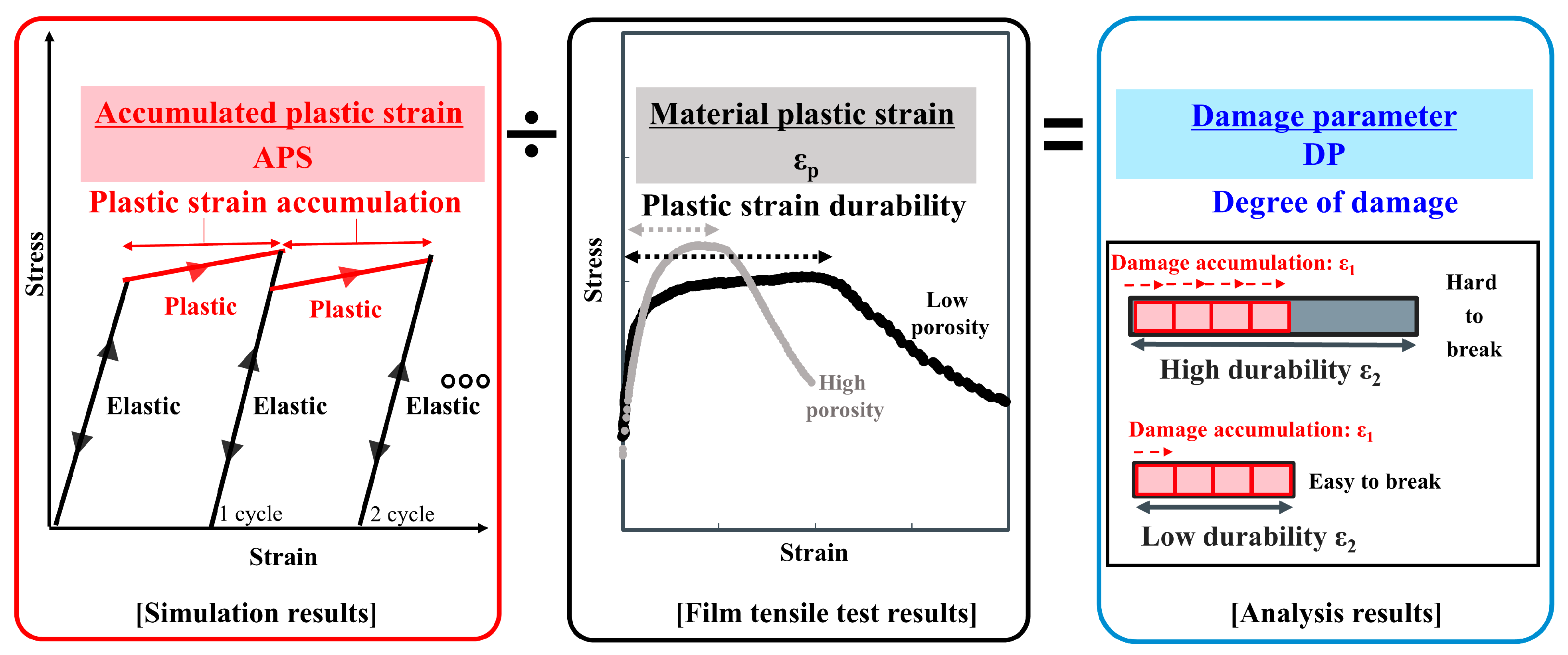
Figure 12 shows the concept of the DP for evaluating the s-Ag die layer degradation assessment correctly [85]. When the stress exceeds the yield point, the s-Ag deforms in plasticity, as is shown on the left side of the red arrow in Figure 11. This plastic deformation is associated with s-Ag’s plastic flow ability, which leads to the degradation of s-Ag during a TST. To date, this degradation has been only assessed by APS, which is defined as the average plastic accumulated von Mises strain value per cycle around the stress concentration area, avoiding the calculated singularity value calculated in the FEA model [98,116,117,118]. However, APS assessment alone cannot describe the difference in plastic flow resistance among the s-Ag materials. As mentioned above, the s-Ag plastic flow resistance differs from the s-Ag originating from porosity differences. Accordingly, the plastic strain value εp of the s-Ag should be included, which is defined as the width of the black dot arrow in Figure 11. Therefore, the DP can be given by
D P = A P S ε p
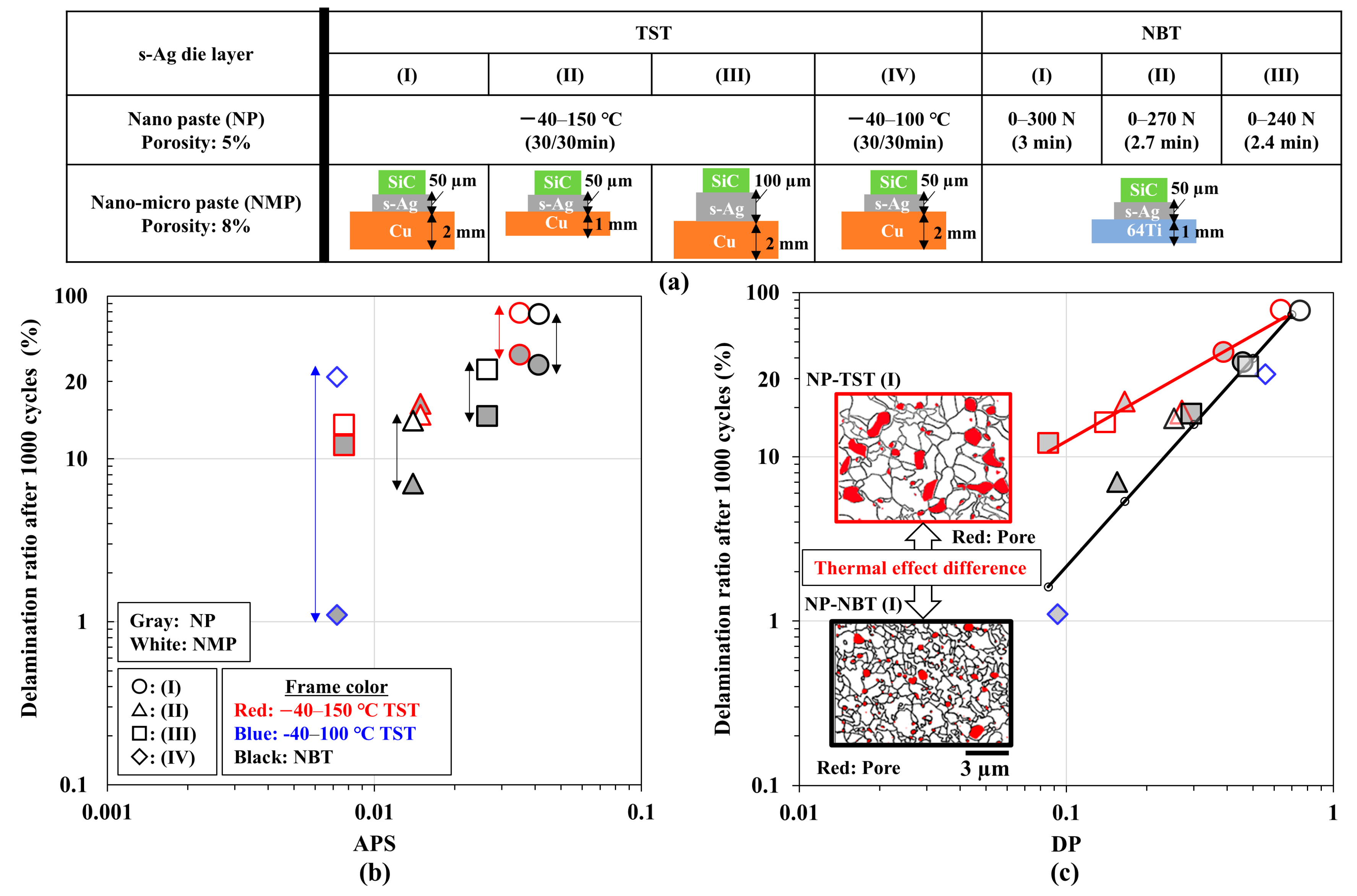
The DP refers to the percentage of a crack that can progress inside the s-Ag layer, irrespective of the s-Ag material. We discuss the DP’s effectiveness in evaluating the s-Ag degradation assessment. Figure 13 summarizes the DP assessment results of two types of Ag pastes’ (NP, nano paste and NMP, nano-micro paste) sintered die layer degradation after a TST and a nine-point bending test (NBT). An NBT is an original bending test developed by the authors, which can be applied to a similar warpage during a TST with mechanical force [99]. This review shows the results of the TSTs, in which temperature controls range between −40 and 150 °C and are controlled by trapezoidal waveform for 60 min per cycle. NBTs force controls from 0 to 240, 270, and 300 N controlled by triangle waveform for 2.4, 2.7, and 3 min, respectively. The NP and NMP are sintered at 300 °C for 10 min at 60 MPa pressure. The s-Ag die-attach assembly’s configuration is shown in Figure 13a. Figure 13b shows the correlation between the delamination ratio after 1000 cycles and the APS, which was conventionally adopted for the die delamination assessment. The gray and white plots are indicative of the NP and NMP, respectively. The difference in plot style is indicative of the test condition differences. The APS and delamination ratios positively correlate in the double logarithmic graph. However, the plots are scattered between the NP and NMP, as indicated by the arrows shown in Figure 13b [119]. Only the APS associated with plastic flow ability in the s-Ag die layer was unsuitable for classifying the failure mode differences among the experiments. By contrast, the plots were well fitted using two linear approximation lines in the double logarithmic graph of the delamination ratio and DP relation, as shown in Figure 13c. That is, the DP is the proper parameter that determines the delamination ratio of the s-Ag die layer, irrespective of s-Ag’s material differences. However, the approximation line slope between red and black differed, suggesting that the failure mode differed. The difference in the thermal effect on the s-Ag die layer gave rise to this difference. Comparing the two NP microstructure observation results after 1000 cycles of TSTs (I) and NBTs (I), as shown in the graph, the pores and crystal grains were found to grow after 1000 cycles of TSTs (I) for the NP. The number of pores decreased to merge into a large pore, originating from the growing crystal grains in a harsh thermal environment. However, the aging effect on the delamination is at most 10%. Accordingly, we should first focus on the DP value in the s-Ag die layer, which mainly determines the delamination ratio of the s-Ag die layer during TSTs. The authors also confirmed that strengthening s-Ag by adding porous CuO causes losses in εp, which leads to accelerated delamination during TSTs [91]. Again, it should be noted that reducing the DP should come first, indicating that our first choice of die material should be a “high ductility material” under the practical use of temperature. The authors will also investigate a new die material, such as a multi-aluminum foil (MAF) [120] die-attach evaluation that can expect to have a higher ductile property than in the s-Ag.
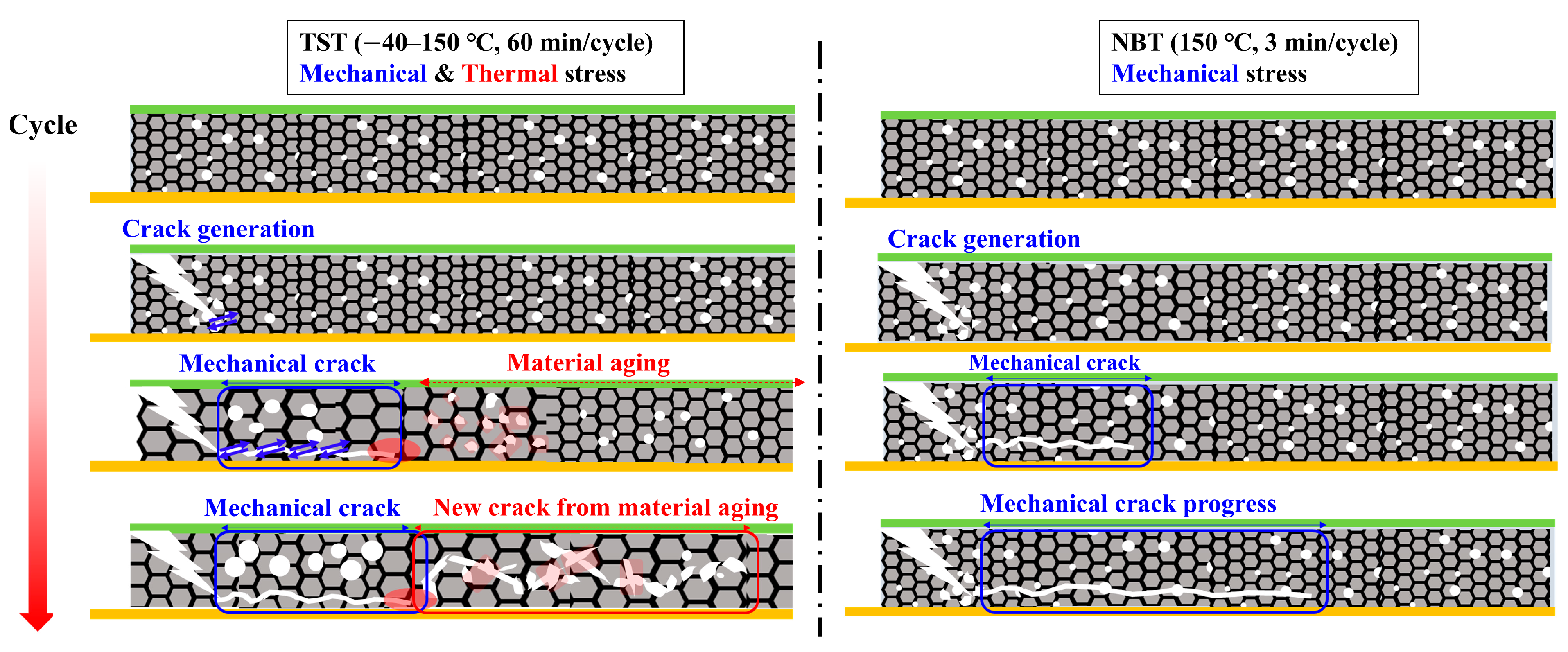
Figure 14 shows an overall primary s-Ag fracture mode schematic image as a function of cycles, considering the experimental results. The upper images illustrate the fracture mode caused by the mechanical and thermal stresses associated with TSTs at harsh temperatures, ranging from −40 to 150 °C. The lower images show the fracture mode caused by only mechanical stress related to the NBT. First, a crack is generated at the upper left corner edge of the s-Ag die layer, where the stress is concentrated after specific cycles. Then, the crack progresses with an inclining angle in both cases. Second, the cracking progresses horizontally and is associated with the maximum shear stress direction at the crack’s tip. The horizontal crack speed is associated with the value of the DP. Apparent cracking behavior is observed regardless of the test type, up to the middle stage. However, in the case of thermal and mechanical stresses, material aging associated with pore growth occurs due to the tensile tension at a high temperature in the inner part of the s-Ag layer, as shown in the third line of illustration on the upper side. Finally, conventional mechanical cracks merge with the new cracks originating from the pore growth, which accelerates and destabilizes the overall cracking speed. In the case of mechanical stress only, the crack still progresses with a straight line at a steady speed because the overall horizontal crack speed would not be affected by the pore growth inside the s-Ag layer.

5. Summary

This paper thoroughly reviewed the characteristics of a Ag paste, the microstructure after the sintering process, the film mechanical properties, and the die degradation assessment by HTS, PCTs, and TSTs. This review paper’s aim was to provide a comprehensive design guideline for packaging products. Understanding the mechanical properties of s-Ag is crucial for designing reliable products with s-Ag die-attach assemblies that can align with the practical use of the products. The film tensile test emerges as a powerful tool for extracting the fundamental mechanical properties of s-Ag. It revealed that s-Ag with minute porosity at around 5% was ideal for achieving high durability. As an essential characteristic of s-Ag, the S–S curve showed the brittle to ductile transition at around 100 °C, indicating that we should care about the temperature effects on s-Ag’s tensile mechanical properties when designing the s-Ag die-attach reliability.
For practical use, reliability tests such as the PCT and TST were essential. For the PCT, the temperature variation speed was high in the s-Ag layer, which created a high-temperature spot surrounding the die area. From the viewpoint of the material characteristics, since the strain speed was high, the tensile mechanical properties of s-Ag always showed a brittle characteristic without plastic deformation. As a result, the cracking mode after the PCT almost showed a vertical crack, ascribed to the principal mechanical tensile stress induced in the longitudinal direction of the substrate, as in a brittle material’s crack. By contrast, for the TST, since the temperature travel time was about 100 times longer than the value in the PCT, the strain speed at the die layer resulted in a small value. The s-Ag die layer mechanical property showed a ductile property at a high temperature operation. As a consequence, the crack in the s-Ag die layer was mainly ascribed to the APS in the s-Ag die layer. We suggested that the cracking speed in the two different types of s-Ag was well fitted by the DP, which is defined as the ratio of APS to the plastic durability obtained from the s-Ag S–S curves. That is, evaluating the DP value prior to performing the TST predicted a degree of delamination after the TST irrespective of the type of s-Ag. In addition, the DP could be categorized as the main fracture mode of the s-Ag during the TST. As for the overall trend, the main contributing factor to the observed degradation was the mechanical stress during the TST.
For the future production of s-Ag die-attach packaging, the focus should be on the failure physics in the reliability design. If the failure physics are clear, we can elaborate on the reliability design prior to prototyping. In other words, we can reduce the amount of material consumed for prototyping because the number of trial and error experiments will be almost zero. Further validations are necessary to apply next generation die materials such as sintered Ag-based composite sheets or MAF. Combining WBG devices and the excellent physical properties of die material will lead to new concepts for the application of products.

Author Contributions

Conceptualization, K.W.; methodology, K.W.; software, K.W.; validation, K.W.; formal analysis, K.W.; investigation, K.W.; resources, K.W.; data curation, K.W.; writing—original draft preparation, K.W.; writing—review and editing, K.W. and T.N.; visualization, K.W.; supervision, T.N.; project administration, T.N. All authors have read and agreed to the published version of the manuscript.

Funding

This research received no external funding.

Institutional Review Board Statement

Not applicable.

Informed Consent Statement

Not applicable.

Conflicts of Interest

Author Keisuke Wakamoto was employed by the company Research and Development Center, ROHM Co., Ltd., the remaining authors declare that the research was conducted in the absence of any commercial or financial relationships that could be construed as a potential conflict of interest.

References

  1. She, X.; Huang, A.Q.; Lucia, O.; Ozpineci, B. Review of Silicon Carbide Power Devices and Their Applications. IEEE Trans. Ind. Electron. 2017, 64, 8193–8205. [Google Scholar] [CrossRef]
  2. Hudgins, J.L.; Simin, G.S.; Santi, E.; Khan, M.A. An assessment of wide bandgap semiconductors for power devices. IEEE Trans. Power Electron. 2003, 18, 907–914. [Google Scholar] [CrossRef]
  3. Biela, J.; Schweizer, M.; Waffler, S.; Kolar, J.W. SiC versus Si—Evaluation of Potentials for Performance Improvement of Inverter and DC–DC Converter Systems by SiC Power Semiconductors. IEEE Trans. Ind. Electron. 2011, 58, 2872–2882. [Google Scholar] [CrossRef]
  4. Neudeck, P.G.; Okojie, R.S.; Chen, L.-Y. High-Temperature Electronics—A Role for Wide Bandgap Semiconductors? Proc. IEEE 2002, 90, 1065–1076. [Google Scholar] [CrossRef]
  5. Gillot, C.; Christian, S.; Massit, C.; Meysenc, L. Double-Sided Cooling for High Power IGBT Modules Using Flip Chip Technology. IEEE Trans. Compon. Packag. Technol. 2001, 24, 698–704. [Google Scholar] [CrossRef]
  6. Charboneau, B.C.; Fei, W.; van Wyk, J.D.; Boroyevich, D.; Zhenxian, L.; Scott, E.P.; Tipton, C.W. Double-Sided Liquid Cooling for Power Semiconductor Devices Using Embedded Power Packaging. IEEE Trans. Ind. Appl. 2008, 44, 1645–1655. [Google Scholar] [CrossRef]
  7. Ishino, H.; Watanabe, T.; Sugiura, K.; Tsuruta, K. 6-in-1 Silicon carbide power module for high performance of power electronics systems. In Proceedings of the 26th International Symposium on Power Semiconductor Devices and ICs (ISPSD), Waikoloa, HI, USA, 15–19 June 2014. [Google Scholar]
  8. Hussein, K.; Ishihara, M.; Miyamoto, N.; Nakata, Y.; Nakano, T. New Compact, High Performance 7th Generation IGBT Module with Direct Liquid Cooling for EV/HEV Inverters. In Proceedings of the 8th Annual IEEE Conference on Applied Power Electronics Conference and Exposition (APEC), Charlotte, NC, USA, 15–19 March 2015. [Google Scholar]
  9. Wen, X.; Fan, T.; Ning, P.; Guo, Q. Technical approaches towards ultra-high power density SiC inverter in electric vehicle applications. CES Trans. Electr. Mach. Syst. 2017, 1, 231–237. [Google Scholar] [CrossRef]
  10. Suganuma, K.; Kim, S.-J.; Kim, K.-S. High-temperature lead-free solders: Properties and possibilities. J. Miner. Met. Mater. Soc. 2009, 61, 64–71. [Google Scholar] [CrossRef]
  11. Schwarzbauer, H. Method of Securing Electronic Components to a Substrate. US4810672, 7 March 1989. [Google Scholar]
  12. Schwarzbauer, H. Method and Apparatus for Fastening Electronic Components to Substrates. US4903885, 27 February 1990. [Google Scholar]
  13. Schwarzbauer, H.; Kuhnert, R. Novel Large Area Joining Technique for Improved Power Device Performance. IEEE Trans. Ind. Appl. 1991, 27, 93–95. [Google Scholar] [CrossRef]
  14. Schwarzbauer, H. Apparatus for Fastening Electronic Components to Substrates. US5058796, 22 October 1991. [Google Scholar]
  15. Siow, K.S. Are Sintered Silver Joints Ready for Use as Interconnect Material in Microelectronic Packaging? J. Electron. Mater. 2014, 43, 947–961. [Google Scholar] [CrossRef]
  16. Fan, J.; Xu, D.; Zhang, H.; Qian, C.; Fan, X.; Zhang, G. Experimental Investigation on the Sintering Kinetics of Nanosilver Particles Used in High-Power Electronic Packaging. IEEE Trans. Compon. Packag. Manuf. Technol. 2020, 10, 1101–1109. [Google Scholar] [CrossRef]
  17. Chen, C.-J.; Chen, C.-M.; Horng, R.-H.; Wuu, D.-S.; Hong, J.-S. Thermal Management and Interfacial Properties in High-Power GaN-Based Light-Emitting Diodes Employing Diamond-Added Sn-3 wt.%Ag-0.5 wt.%Cu Solder as a Die-Attach Material. J. Electron. Mater. 2010, 39, 2618–2626. [Google Scholar] [CrossRef]
  18. Youssef, T.; Rmili, W.; Woirgard, E.; Azzopardi, S.; Vivet, N.; Martineau, D.; Meuret, R.; Le Quilliec, G.; Richard, C. Power modules die attach: A comprehensive evolution of the nanosilver sintering physical properties versus its porosity. Microelectron. Reliab. 2015, 55, 1997–2002. [Google Scholar] [CrossRef]
  19. Ordonez-Miranda, J.; Hermens, M.; Nikitin, I.; Kouznetsova, V.G.; van der Sluis, O.; Ras, M.A.; Reparaz, J.S.; Wagner, M.R.; Sledzinska, M.; Gomis-Bresco, J.; et al. Measurement and modeling of the effective thermal conductivity of sintered silver pastes. Int. J. Therm. Sci. 2016, 108, 185–194. [Google Scholar] [CrossRef]
  20. Lv, W.; Liu, J.; Lei, X.; Zhu, F. Porosity Dependence of Thermal and Electrical Properties in Nano-Silver Paste. IEEE Trans. Electron Devices 2023, 70, 702–707. [Google Scholar] [CrossRef]
  21. ECPE Guideline AQG 324: Qualification of Power Modules for Use in Power Electronics Converter Units in Motor Vehicles; ECPE European Center for Power Electronics e.V.: Nuremberg, Germany, 2019.
  22. Hung, T.Y.; Chiang, S.Y.; Huang, C.J.; Lee, C.C.; Chiang, K.N. Thermal–mechanical behavior of the bonding wire for a power module for a power module subjected to the power cycling test. Microelectron. Reliab. 2011, 51, 1819–1823. [Google Scholar] [CrossRef]
  23. Herboth, T.; Fruh, C.; Gunther, M.; Wilde, J. Assessment of Thermo-Mechanical Stresses in Low Temperature Joining Technology. In Proceedings of the 13th International Thermal, Mechanical and Multi-Physics Simulation and Experiments in Microelectronics and Microsystems (EurosimE), Cascais, Portugal, 16–18 April 2012. [Google Scholar]
  24. Gorecki, P.; Gorecki, K.; Kisiel, R.; Brzozowski, E.; Bar, J.; Guziewicz, M. Investigations of an Influence of the Assembling Method of the Die to the Case on Thermal Parameters of IGBTs. IEEE Trans. Compon. Packag. Manuf. Technol. 2021, 11, 1988–1996. [Google Scholar] [CrossRef]
  25. Dai, J.; Li, J.; Agyakwa, P.; Corfield, M.; Johnson, C.M. Comparative Thermal and Structural Characterization of Sintered Nano-Silver and High-Lead Solder Die Attachments During Power Cycling. IEEE Trans. Device Mater. Reliab. 2018, 18, 256–265. [Google Scholar] [CrossRef]
  26. Ng, W.; Kumagai, K.; Sweatman, K.; Nishimura, T. The impacts of process sequence on the quality of pressurized sintered silver joints. In Proceedings of the 17th Electronics Packaging Technology Conference (EPTC), Suntec City, Singapore, 2–4 December 2015. [Google Scholar]
  27. Wereszczak, A.A.; Modugno, M.C.; Chen, B.R.; Carty, W.M. Contact Drying of Printed Sinterable-Silver Paste. IEEE Trans. Compon. Packag. Manuf. Technol. 2017, 7, 2079–2086. [Google Scholar] [CrossRef]
  28. Yasugi, D.; Wakamoto, K.; Kumakiri, Y.; Namazu, T. Formation of Wavy Crack in Double-Layered Ag and CuO/Ag Sintering Die Attach Assemblies Subjected to Thermal Shock Testing. IEEE Trans. Compon. Packag. Manuf. Technol. 2024, 14, 593–600. [Google Scholar] [CrossRef]
  29. Peng, P.; Hu, A.; Gerlich, A.P.; Zou, G.; Liu, L.; Zhou, Y.N. Joining of Silver Nanomaterials at Low Temperatures: Processes, Properties, and Applications. ACS Appl. Mater. Interfaces 2015, 7, 12597–12618. [Google Scholar] [CrossRef] [PubMed]
  30. Zhang, H.; Jiu, J.; Suzuki, Y.; Akai, Y.; Suganuma, K. Effect of solvents on sintering behaviors of silver paste for power-device packaging. In Proceedings of the PCIM Asia 2016; International Exhibition and Conference for Power Electronics, Intelligent Motion, Renewable Energy and Energy Management, Shanghai, China, 28–30 June 2016. [Google Scholar]
  31. Jiu, J.; Zhang, H.; Koga, S.; Nagao, S.; Izumi, Y.; Suganuma, K. Simultaneous synthesis of nano and micro-Ag particles and their application as a die-attachment material. J. Mater. Sci. Mater. Electron. 2015, 26, 7183–7191. [Google Scholar] [CrossRef]
  32. Lei, T.G.; Calata, J.N.; Lu, G.-Q.; Chen, X.; Luo, S. Low-Temperature Sintering of Nanoscale Silver Paste for Attaching Large-Area (>100 mm2) Chips. IEEE Trans. Compon. Packag. Technol. 2010, 33, 98–104. [Google Scholar] [CrossRef]
  33. Zhang, H.; Nagao, S.; Suganuma, K.; Albrecht, H.-J.; Wilke, K. Thermostable Ag die-attach structure for high-temperature power devices. J. Mater. Sci. Mater. Electron. 2015, 27, 1337–1344. [Google Scholar] [CrossRef]
  34. Wang, M.; Mei, Y.; Hu, W.; Li, X.; Lu, G.-Q. Pressureless Sintered-Silver as Die Attachment for bonding Si and SiC Chips on Silver, Gold, Copper, and Nickel Metallization for Power Electronics Packaging: The Practice and Science. IEEE J. Emerg. Sel. Top. Power Electron. 2022, 10, 2645–2655. [Google Scholar] [CrossRef]
  35. Chen, C.; Suganuma, K. Microstructure and mechanical properties of sintered Ag particles with flake and spherical shape from nano to micro size. Mater. Des. 2019, 162, 311–321. [Google Scholar] [CrossRef]
  36. Bai, J.G.; Zhang, Z.Z.; Calata, J.N.; Lu, G.Q. Low-Temperature Sintered Nanoscale Silver as a Novel Semiconductor Device-Metallized Substrate Interconnect Material. IEEE Trans. Compon. Packag. Technol. 2006, 29, 589–593. [Google Scholar] [CrossRef]
  37. Li, J.; Johnson, C.M.; Buttay, C.; Sabbah, W.; Azzopardi, S. Bonding strength of multiple SiC die attachment prepared by sintering of Ag nanoparticles. J. Mater. Process. Technol. 2015, 215, 299–308. [Google Scholar] [CrossRef]
  38. Chua, S.T.; Siow, K.S. Microstructural studies and bonding strength of pressureless sintered nano-silver joints on silver, direct bond copper (DBC) and copper substrates aged at 300 °C. J. Alloys Compd. 2016, 687, 486–498. [Google Scholar] [CrossRef]
  39. Chew, L.M.; Schmitt, W.; Dubis, M. High bonding strength of silver sintered joints on non-precious metal surfaces by pressure sintering under air atmosphere using micro-silver sinter paste. In Proceedings of the 20th Electronics Packaging Technology Conference (EPTC), Sentona, Singapore, 4–7 December 2018. [Google Scholar]
  40. Kim, D.; Chen, C.; Nagao, S.; Suganuma, K. Mechanical characteristics and fracture behavior of GaN/DBA die-attached during thermal aging: Pressure-less hybrid Ag sinter joint and Pb–5Sn solder joint. J. Mater. Sci. Mater. Electron. 2019, 31, 587–598. [Google Scholar] [CrossRef]
  41. Yeom, J.; Nagao, S.; Chen, C.; Sugahara, T.; Zhang, H.; Choe, C.; Li, C.-F.; Suganuma, K. Ag particles for sinter bonding: Flakes or spheres? Appl. Phys. Lett. 2019, 114, 253103. [Google Scholar] [CrossRef]
  42. Chen, C.; Kim, D.; Zhang, Z.; Wakasugi, N.; Liu, Y.; Hsieh, M.-C.; Zhao, S.; Suetake, A.; Suganuma, K. Interface-Mechanical and Thermal Characteristics of Ag Sinter Joining on Bare DBA Substrate During Aging, Thermal Shock and 1200 W/cm2 Power Cycling Tests. IEEE Trans. Power Electron. 2022, 37, 6647–6659. [Google Scholar] [CrossRef]
  43. Hirose, A.; Tatsumi, H.; Takeda, N.; Akada, Y.; Ogura, T.; Ide, E.; Morita, T. A novel metal-to-metal bonding process through in-situ formation of Ag nanoparticles using Ag2O microparticles. J. Phys. Conf. Ser. 2009, 165, 012074. [Google Scholar] [CrossRef]
  44. Matsuhisa, N.; Inoue, D.; Zalar, P.; Jin, H.; Matsuba, Y.; Itoh, A.; Yokota, T.; Hashizume, D.; Someya, T. Printable elastic conductors by in situ formation of silver nanoparticles from silver flakes. Nat. Mater. 2017, 16, 834–840. [Google Scholar] [CrossRef] [PubMed]
  45. Glover, D.R.; Miller, M.J.; Hutchison, E.J. Generation of Metal Nanoparticles from Silver and Copper Objects: Nanoparticle Dynamics on Surfaces and Potential Sources of Nanoparticles in the Environment. ACS Nano 2011, 5, 8950–8957. [Google Scholar] [CrossRef]
  46. Rybak, B.M.; Ornatska, M.; Bergman, K.N.; Genson, K.L.; Tsukruk, V.V. Formation of Silver Nanoparticles at the Air–Water Interface Mediated by a Monolayer of Functionalized Hyperbranched Molecules. Langmuir 2006, 22, 1027–1037. [Google Scholar] [CrossRef] [PubMed]
  47. Allen, G.L.; Bayles, R.A.; Gile, W.W.; Jesser, W.A. Small particle melring of pure metals. Thin Solid Film. 1986, 144, 297–308. [Google Scholar] [CrossRef]
  48. Asama, K.; Matsuda, T.; Ogura, T.; Sano, T.; Takahashi, M.; Hirose, A. Low-temperature metal-to-alumina direct bonding process utilizing redox reaction between silver oxide and organic agent. Mater. Sci. Eng. A 2017, 702, 398–405. [Google Scholar] [CrossRef]
  49. Matsuda, T.; Inami, K.; Motoyama, K.; Sano, T.; Hirose, A. Silver oxide decomposition mediated direct bonding of silicon-based materials. Sci. Rep. 2018, 8, 10472. [Google Scholar] [CrossRef]
  50. Inami, K.; Matsuda, T.; Kawabata, R.; Sano, T.; Hirose, A. Lowering bonding temperature for silver sintering to silicon and silicon carbide using silver oxide decomposition. J. Mater. Sci. Mater. Electron. 2020, 31, 16511–16518. [Google Scholar] [CrossRef]
  51. Kawabata, R.; Matsuda, T.; Seo, R.; Hirose, A. Metallization-free silver sinter bonding to silicon via in situ decomposition of silver oxalate. Mater. Lett. 2021, 300, 130205. [Google Scholar] [CrossRef]
  52. Matsuda, T.; Kawabata, R.; Okamoto, T.; Hirose, A. Ag Sinter Bonding to Si Substrate via Temporal Formation and Decomposition of Ag Carboxylate. Nanomaterials 2023, 13, 2292. [Google Scholar] [CrossRef]
  53. Wakamoto, K.; Mochizuki, Y.; Otsuka, T.; Nakahara, K.; Namazu, T. Tensile mechanical properties of sintered porous silver films and their dependence on porosity. Jpn. J. Appl. Phys. 2019, 58, SDDL08. [Google Scholar] [CrossRef]
  54. Esa, S.R.; Omar, G.; Fadzullah Md, S.; Siow, K.S.; Rahim Abdul, B. The evolutions of microstructure in pressureless sintered silver die attach material. Int. J. Nanoelectron. Mater. 2021, 14, 179–194. [Google Scholar]
  55. Carr, J.; Milhet, X.; Gadaud, P.; Boyer, S.A.E.; Thompson, G.E.; Lee, P. Quantitative characterization of porosity and determination of elastic modulus for sintered micro-silver joints. J. Mater. Process. Technol. 2015, 225, 19–23. [Google Scholar] [CrossRef]
  56. Rmili, W.; Vivet, N.; Chupin, S.; Le Bihan, T.; Le Quilliec, G.; Richard, C. Quantitative Analysis of Porosity and Transport Properties by FIB-SEM 3D Imaging of a Solder Based Sintered Silver for a New Microelectronic Component. J. Electron. Mater. 2016, 45, 2242–2251. [Google Scholar] [CrossRef]
  57. Zabihzadeh, S.; Van Petegem, S.; Holler, M.; Diaz, A.; Duarte, L.I.; Van Swygenhoven, H. Deformation behavior of nanoporous polycrystalline silver. Part I: Microstructure and mechanical properties. Acta Mater. 2017, 131, 467–474. [Google Scholar] [CrossRef]
  58. Meyghani, B.; Awang, M.; Bokam, P.; Plank, B.; Heinzl, C.; Siow, K.S. Finite element modeling of nano porous sintered silver material using computed tomography images. Materialwiss. Werkst. 2019, 50, 533–538. [Google Scholar] [CrossRef]
  59. Kim, D.; Kim, M.-S. Macroscale and microscale structural mechanisms capable of delaying the fracture of low-temperature and rapid pressureless Ag sintered electronics packaging. Mater. Charact. 2023, 198, 112758. [Google Scholar] [CrossRef]
  60. Chen, C.; Nagao, S.; Zhang, H.; Jiu, J.; Sugahara, T.; Suganuma, K.; Iwashige, T.; Sugiura, K.; Tsuruta, K. Mechanical Deformation of Sintered Porous Ag Die Attach at High Temperature and Its Size Effect for Wide-Bandgap Power Device Design. J. Electron. Mater. 2016, 46, 1576–1586. [Google Scholar] [CrossRef]
  61. Weber, C.; Walter, H.; Van Dijk, M.; Hutter, M.; Wittler, O.; Lang, K.-D. Combination of Experimental and Simulation Methods for Analysis of Sintered Ag Joints for High Temperature Applications. In Proceedings of the 66th Electronic Components and Technology Conference (ECTC), Las Vegas, NV, USA, 31 May–3 June 2016. [Google Scholar]
  62. Namazu, T.; Inoue, S.; Takemoto, H.; Koterazawa, K. Mechanical properties of Poly crystalline Titanium Nitride Films Measured by XRD Tensile Testing. IEEJ Trans. SM 2005, 125, 374–379. [Google Scholar] [CrossRef]
  63. Namazu, T.; Inoue, S.; Ano, D.; Koterazawa, K. XRD Tensile Test Technique to Measure Mechanical Properties of Micron-Thick Si and TiN Films. Key Eng. Mater. 2005, 297–300, 574–580. [Google Scholar] [CrossRef]
  64. Namazu, T. Mechanical Property Measurement of Micro/Nanoscale Materials for MEMS: A Review. IEEJ Trans. Electr. Electron. Eng. 2022, 18, 308–324. [Google Scholar] [CrossRef]
  65. Komatsubara, M.; Namazu, T.; Nagai, Y.; Inoue, S.; Naka, N.; Kashiwagi, S.; Ohtsuki, K. Raman Spectrum Curve Fitting for Estimating Surface Stress Distribution in Single-Crystal Silicon Microstructure. Jpn. J. Appl. Phys. 2009, 48, 04C021. [Google Scholar] [CrossRef]
  66. Naka, N.; Kashiwagi, S.; Nagai, Y.; Namazu, T. Micro-Raman spectroscopic analysis of single crystal silicon microstructures for surface stress mapping. Jpn. J. Appl. Phys. 2015, 54, 106601. [Google Scholar] [CrossRef]
  67. Nemat-Nasser, S. Mechanical Testing and Evaluation; ASM International: Materials Park, OH, USA, 2001; Volume 8, pp. 462–467. [Google Scholar]
  68. Herboth, T.; Guenther, M.; Fix, A.; Wilde, J. Failure Mechanisms of Sintered Silver Interconnections for Power Electronic Applications. In Proceedings of the 63rd Electronic Components and Technology Conference (ECTC), Las Vegas, NV, USA, 28–31 May 2013. [Google Scholar]
  69. Caccuri, V.; Milhet, X.; Gadaud, P.; Bertheau, D.; Gerland, M. Mechanical Properties of Sintered Ag as a New Material for Die Bonding: Influence of the Density. J. Electron. Mater. 2014, 43, 4510–4514. [Google Scholar] [CrossRef]
  70. Milhet, X.; Gadaud, P.; Caccuri, V.; Bertheau, D.; Mellier, D.; Gerland, M. Influence of the Porous Microstructure on the Elastic Properties of Sintered Ag Paste as Replacement Material for Die Attachment. J. Electron. Mater. 2015, 44, 3948–3956. [Google Scholar] [CrossRef]
  71. Suzuki, T.; Yasuda, Y.; Terasaki, T.; Morita, T.; Kawana, Y.; Ishikawa, D.; Nishimura, M.; Nakako, H.; Kurafuchi, K.; Matsuda, T. Tensile-Fatigue Behavior of Sintered Copper Die-Attach Material. IEEE Trans. Device Mater. Reliab. 2019, 19, 461–467. [Google Scholar] [CrossRef]
  72. Mochizuki, Y.; Wakamoto, K.; Otsuka, T.; Nakahara, K.; Namazu, T. Degradation mechanism of sintered porous silver film at elevated temperatures. In Proceedings of the 32nd International Microprocesses Nanotechnology Conference (MNC), Hiroshima, Japan, 28–31 October 2019. [Google Scholar]
  73. Wakamoto, K.; Mochizuki, Y.; Otsuka, T.; Nakahara, K.; Namazu, T. Temperature Dependence on Tensile Mechanical Properties of Sintered Silver Film. Materials 2020, 13, 4061. [Google Scholar] [CrossRef]
  74. Chen, X.; Li, R.; Qi, K.; Lu, G.-Q. Tensile Behaviors and Ratcheting Effects of Partially Sintered Chip-Attachment Films of a Nanoscale Silver Paste. J. Electron. Mater. 2008, 37, 1574–1579. [Google Scholar] [CrossRef]
  75. Nikitin, I.; Pressel, K. Mechanical Properties of Porous Silver Materials Depending on Sintering Parameters. In Proceedings of the 20th InternatIonal Workshop on Thermal Investigations of ICs and Systems (THERMINIC), Greenwich, UK, 24–26 September 2014. [Google Scholar]
  76. Tatsumi, H.; Kumada, S.; Fukuda, A.; Yamaguchi, H.; Kashiba, Y. Impact of Metallurgical and Mechanical Properties of Sintered Silver Joints on Die-Attach Reliability of High-Temperature Power Modules. J. Microelectron. Electron. Packag. 2016, 13, 121–127. [Google Scholar] [CrossRef]
  77. Wakamoto, K.; Yasugi, D.; Otsuka, T.; Nakahara, K.; Namazu, T. Fracture Mechanism of Sintered Silver Film Revealed by In Situ SEM Uniaxial Tensile Loading. IEEE Trans. Compon. Packag. Manuf. Technol. 2024, 14, 240–250. [Google Scholar] [CrossRef]
  78. Ashby, M.F. Boundary Defects and Atomic Aspects of Boundary Slidin and Diffusional Creep. Surf. Sci. 1972, 31, 498–542. [Google Scholar] [CrossRef]
  79. Alarifi, H.A.; Atis, M.; Ozdogan, C.; Hu, A.; Yavuz, M.; Zhou, Y. Molecular Dynamics Simulation of Sintering and Surface Premelting of Silver Nanoparticles. Mater. Trans. 2013, 54, 884–889. [Google Scholar] [CrossRef]
  80. Sommer, J.; Herzig, C. Direct determination of grain-boundary and dislocation self-diffusion coefficients in silver from experiments in type-C kinetics. J. Appl. Phys. 1992, 72, 2758–2766. [Google Scholar] [CrossRef]
  81. Calabretta, M.; Sitta, A.; Oliveri, S.M.; Sequenzia, G. Silver Sintering for Silicon Carbide Die Attach: Process Optimization and Structural Modeling. Appl. Sci. 2021, 11, 7012. [Google Scholar] [CrossRef]
  82. Paknejad, S.A.; Mansourian, A.; Greenberg, J.; Khtatba, K.; Van Parijs, L.; Mannan, S.H. Microstructural evolution of sintered silver at elevated temperatures. Microelectron. Reliab. 2016, 63, 125–133. [Google Scholar] [CrossRef]
  83. Gadaud, P.; Caccuri, V.; Bertheau, D.; Carr, J.; Milhet, X. Ageing sintered silver: Relationship between tensile behavior, mechanical properties and the nanoporous structure evolution. Mater. Sci. Eng. A 2016, 669, 379–386. [Google Scholar] [CrossRef]
  84. Yu, F.; Cui, J.; Zhou, Z.; Fang, K.; Johnson, R.W.; Hamilton, M.C. Reliability of Ag Sintering for Power Semiconductor Die Attach in High-Temperature Applications. IEEE Trans. Power Electron. 2017, 32, 7083–7095. [Google Scholar] [CrossRef]
  85. Wakamoto, K.; Otsuka, T.; Nakahara, K.; Mugilgeethan, V.; Matsumoto, R.; Namazu, T. Degradation Mechanism of Silver Sintering Die Attach Based on Thermal and Mechanical Reliability Testing. IEEE Trans. Compon. Packag. Manuf. Technol. 2023, 13, 197–210. [Google Scholar] [CrossRef]
  86. Paknejad, S.A.; Khtatba, K.; Mansourian, A.; Mannan, S.H. Ultra-Stable Sintered Silver Die Attach for Demanding High-Power/Temperature Applications. IEEE Trans. Device Mater. Reliab. 2017, 17, 795–798. [Google Scholar] [CrossRef]
  87. Khtatba, K.; Paknejad, S.A.; Al Zoubi, T.; Qutaish, H.; Sano, N.; Mannan, S.H. Arresting high-temperature microstructural evolution inside sintered silver. J. Mater. Sci. Mater. Electron. 2018, 30, 463–474. [Google Scholar] [CrossRef]
  88. Zhang, H.; Nagao, S.; Suganuma, K. Addition of SiC Particles to Ag Die-Attach Paste to Improve High-Temperature Stability; Grain Growth Kinetics of Sintered Porous Ag. J. Electron. Mater. 2015, 44, 3896–3903. [Google Scholar] [CrossRef]
  89. Heuck, N.; Langer, A.; Stranz, A.; Palm, G.; Sittig, R.; Bakin, A.; Waag, A. Analysis and Modeling of Thermomechanically Improved Silver-Sintered Die-Attach Layers Modified by Additives. IEEE Trans. Compon. Packag. Manuf. Technol. 2011, 1, 1846–1855. [Google Scholar] [CrossRef]
  90. Xu, Y.; Qiu, X.; Li, W.; Wang, S.; Ma, N.; Ueshima, M.; Chen, C.; Suganuma, K. Development of high thermal conductivity of Ag/diamond composite sintering paste and its thermal shock reliability evaluation in SiC power modules. J. Mater. Res. Technol. 2023, 26, 1079–1093. [Google Scholar] [CrossRef]
  91. Wakamoto, K.; Kumakiri, Y.; Namazu, T. Mechanical property changes in sintered silver films by including copper oxide nanoparticles. Microelectron. Reliab. 2024, 153, 115322. [Google Scholar] [CrossRef]
  92. Dudek, R.; Doring, R.; Rzepca, S.; Ehrhardt, C.; Hultter, M.; Rudzki, J.; Osterwald, F.; Eisele, R.; Stegmeiser, S.; Weidner, K.; et al. Investigations on Power Cycling Induced Fatigue Failure of IGBTs with Silver Sintered Interconnects. In Proceedings of the 2015 European Microelectronics Packaging Conference, Fredrichshafen, Germany, 14–16 September 2015. [Google Scholar]
  93. Dudel, R.; Doring, R.; Rzepka, S.; Ehrhardt, C.; Gunther, M.; Haag, M. Electro-Thermo-Mechanical Analyses on Silver Sintered IGBT-Module Reliability in Power Cycling. In Proceedings of the 16th International Conference on Thermal, Mechanical and Multi-Physics Simulation and Experiments in Microelectronics and Microsystems (EuroSimE), Budapest, Hungary, 19–22 April 2015. [Google Scholar]
  94. Webber, C.; Hutter, M.; Schmitz, S.; Lang, K.-D. Dependency of the Porosity and the Layer Thickness on the Reliability of Ag Sintered Joints during Active Power Cycling. In Proceedings of the 65th Electronic Components and Technology Conference (ECTC), San Diego, CA, USA, 26–29 May 2015. [Google Scholar]
  95. Kosuge, H.; Kawabata, T.; Okita, T.; Nako, H. Accurate Estimation of Brittle Fracture Toughness Deterioration in Steel Structures Subjected to Large Complicated Prestrains. Crystals 2020, 10, 867. [Google Scholar] [CrossRef]
  96. Cui, H. Accelerated Temperature Cycle Test and Coffin-Manson Model for Electronic Packaging. In Proceedings of the Annual Reliability and Maintainability Symposium, Alexandria, VA, USA, 24–27 January 2005. [Google Scholar]
  97. Herboth, T.; Guenther, M.; Zeiser, R.; Wilde, J. Investigation of Stress States in Silicon Dies Induced by the Low Temperature Joining Technology. In Proceedings of the 14th International Conference on Thermal, Mechanical and Multi-Physics Simulation and Experiments in Microelectronics and Microsystems, (EuroSimE), Wroclaw, Poland, 14–17 April 2013. [Google Scholar]
  98. Rajaguru, P.; Lu, H.; Bailey, C. Sintered silver finite element modelling and reliability based design optimisation in power electronic module. Microelectron. Reliab. 2015, 55, 919–930. [Google Scholar] [CrossRef]
  99. Wakamoto, K.; Fuji, K.; Otsuka, T.; Nakahara, K.; Namazu, T. Nine Point Bending Test Technique for Understanding of Sintered Silver Die Bonding Failure Mechanism. Exp. Tech. 2024, 48, 399–408. [Google Scholar] [CrossRef]
  100. Schaal, M.; Klingler, M.; Metais, B.; Gruninger, R.; Hoffmann, S.; Wunderle, B. Reliability Assessment of Ag Sintered Joints Using a SiC Semiconductor and Determination of Failure Mechanism in the Field of Power Electronics. In Proceedings of the 21st International Conference on Thermal, Mechanical and Multi-Physics Simulation and Experiments in Microelectronics and Microsystems (EuroSimE), Cracow, Poland, 5–8 July 2020. [Google Scholar]
  101. Santopa, M.; Russo, S.; Torrisi, M.; Renna, M.; Sitta, A.; Calabretta, M. Fast transient thermomechanical stress to set a pressure-assisted sintering process. In Proceedings of the 15th Conference on Ph.D Research in Microelectronics and Electronics (PRIME), Lausanne, Switzerland, 15–18 July 2019. [Google Scholar]
  102. Heilmann, J.; Nikitin, I.; Zschenderlein, U.; May, D.; Pressel, K.; Wunderle, B. Reliability experiments of sintered silver based interconnections by accelerated isothermal bending tests. Microelectron. Reliab. 2017, 74, 136–146. [Google Scholar] [CrossRef]
  103. Wakamoto, K.; Kumakiri, Y.; Otsuka, T.; Nakahara, K.; Namazu, T. Comparison of sintered silver die attach failure between thermal shock test and mechanical cycling test. Jpn. J. Appl. Phys. 2022, 61, SD1029. [Google Scholar] [CrossRef]
  104. Heilmann, J.; Wunderle, B.; Zschenderlein, U.; Wille, C.; Pressel, K. Physics of failure based lifetime modelling for sintered silver die attach in power electronics: Accelerated stress testing by isothermal bending and thermal shock in comparison. Microelectron. Reliab. 2023, 145, 114973. [Google Scholar] [CrossRef]
  105. Forndran, F.; Heilmann, J.; Metzler, M.; Leicht, M.; Wunderle, B. A Parametric Simulative Study for Lifetime Prediction of Sintered Silver Die Attach Under Different Accelerated Testing Conditions. In Proceedings of the 22nd International Conference on Thermal, Mechanical and Multi-Physics Simulation and Experiments in Microelectronics and Microsystems (EuroSimE), St. Julian, Malta, 19–21 April 2021. [Google Scholar]
  106. Onaka, S.; Kato, M.; Soeta, S.; Mori, T. A New Approach for Diffusional Growth of Grain-Boundary Voids. Trans. Jpn. Inst. Met. 1988, 29, 284–291. [Google Scholar] [CrossRef]
  107. Onaka, S.; Kato, M. Unified Analysis for Various Diffusion-controlled Deformation and Fracture Processes. ISIJ Int. 1991, 31, 331–341. [Google Scholar] [CrossRef]
  108. Mathew, A.; Dudek, R.; Otto, A.; Scherf, C.; Rzepka, S.; Subbiah, N.; Rane, K.A.; Wilde, J. Lifetime modelling of sintered silver interconnected power devices by FEM and experiment. In Proceedings of the 22nd International Conference on Thermal, Mechanical and Multi-Physics Simulation and Experiments in Microelectronics and Microsystems (EuroSimE), St. Julian, Malta, 19–21 April 2021. [Google Scholar]
  109. Mathew, A.; Dudek, R.; Otto, A.; Scherf, C.; Rzepka, S.; Subbiah, N.; Rane, K.A.; Wilde, J. Investigation of reliability issues in sintered silver interconnected power devices and its lifetime prediction by FEM and experiment. In Proceedings of the 12th International Conference on Integrated Power Electronics Systems (CIPS), Berlin, Germany, 15–17 March 2022. [Google Scholar]
  110. Choe, C.; Chen, C.; Noh, S.; Suganuma, K. Thermal Shock Performance of DBA/AMB Substrates Plated by Ni and Ni-P Layers for High-Temperature Applications of Power Device Modules. Materials 2018, 11, 2394. [Google Scholar] [CrossRef] [PubMed]
  111. Cordero, Z.C.; Knight, B.E.; Schuh, C.A. Six decades of the Hall–Petch effect—A survey of grain-size strengthening studies on pure metals. Int. Mater. Rev. 2016, 61, 495–512. [Google Scholar] [CrossRef]
  112. Nishimoto, S.; Moeini, S.A.; Ohashi, T.; Nagatomo, Y.; McCluskey, P. Novel silver die-attach technology on silver pre-sintered DBA substrates for high temperature applications. Microelectron. Reliab. 2018, 87, 232–237. [Google Scholar] [CrossRef]
  113. Wakamoto, K.; Otsuka, T.; Nakahara, K.; Namazu, T. Degradation Mechanism of Pressure-Assisted Sintered Silver by Thermal Shock Test. Energies 2021, 14, 5532. [Google Scholar] [CrossRef]
  114. Knoerr, M.; Kraft, S.; Schletz, A. Reliability assessment of sintered nano-silver die attachment for power semiconductors. In Proceedings of the 12th Electronics Packaging Technology Conference (EPTC), Singapore, 8–10 December 2010. [Google Scholar]
  115. Jiang, N.; Chen, M.; Xu, S.; Lai, W.; Bin, G.; Chen, Y. Lifetime Evaluation of Solder Layer in an IGBT Module under Different Temperature Levels. In Proceedings of the 8th International Power Electronics and Motion Control Conference (IPEMC-ECCE Asia), Hefei, China, 22–26 May 2016. [Google Scholar]
  116. Forndran, F.; Heilmann, J.; Metzler, M.; Leicht, M.; Wunderle, B. Determination of Rate- and Temperature Dependent Inelastic Material Data for Sintered Silver Die Attach and Simulative Implementation. In Proceedings of the 23rd International Conference on Thermal, Mechanical and Multi-Physics Simulation and Experiments in Microelectronics and Microsystems (EuroSimE), St. Julian, Malta, 25–27 April 2022. [Google Scholar]
  117. Wilde, J.; Staiger, W.; Thoben, M.; Schuch, B.; Kilian, H. Integration of Liquid Cooling, Thermal and Thermomechanical Design for the Lifetime Prediction of Electrical Power Modules. In Proceedings of the International Congress and Exposition, Detroit, MI, USA, 23–26 February 1998. [Google Scholar]
  118. Wunderle, B.; Becker, K.F.; Sinning, R.; Wittler, O.; Schacht, R.; Walter, H.; Schneider-Ramelow, M.; Halser, K.; Simper, N.; Michel, B.; et al. Thermo-mechanical reliability during technology development of power chip-on-board assemblies with encapsulation. Microsyst. Technol. 2009, 15, 1467–1478. [Google Scholar] [CrossRef]
  119. Wakamoto, K. Mechanical Reliability of Sintered Nano Silver for Power Device Packaging. Ph.D. Thesis, Kyoyo University of Advanced Science, Kyoto, Japan, 22 March 2023. [Google Scholar]
  120. Chen, C.; Suganuma, K. Low temperature SiC die-attach bonding technology by hillocks generation on Al sheet surface with stress self-generation and self-release. Sci. Rep. 2020, 10, 9042. [Google Scholar] [CrossRef] [PubMed]
Figure 1. Representative s-Ag die bonding process schematic image.
Energies 17 04105 g001
Figure 2. SEM photographs of Ag particles adopted in the Ag paste in (a) nano particle, (b) micro particle, and (c) nano-micro (flake) particle [35].
Energies 17 04105 g002
Figure 3. Cross-sectional EBSD analysis results of submicron s-Ag layer by changing sintering temperature at 175, 200, 225, and 250 °C for 10 min without applied process pressure [59].
Energies 17 04105 g003
Figure 4. Cross-sectional SEM observation results of nano-s-Ag layer by changing sintering process pressure at 5, 10, 30, and 60 MPa at 300 °C for 10 min pressure [53].
Energies 17 04105 g004
Figure 5. (a) S–S curves for each s-Ag film, as introduced in Figure 3 and (b) their mechanical properties (Apparent Young’s modulus, Ultimate tensile strength, and Breaking strain) as a function of porosity. (Red: 60 MPa, Orange: 30 MPa, Blue: 10 MPa, and Pale: 5 MPa pressure of -sAg) [53].
Energies 17 04105 g005
Figure 6. (a) S–S curves for nano-s-Ag film at different temperatures and (b) fracture surface observation results after tensile tests at different temperatures [77].
Energies 17 04105 g006
Figure 7. In situ SEM tensile test results of force and time relations and SEM snapshots along with image-processed results at (a) RT and (b) 300 °C [77].
Energies 17 04105 g007
Figure 8. s-Ag fracture mechanism schematic view [77].
Energies 17 04105 g008
Figure 9. Nano-s-Ag microstructure changes after HTS (150 °C for 500 h) observed by cross-sectional SEM images.
Energies 17 04105 g009
Figure 10. Cross-sectional SEM images of the s-Ag die layer after 116,357 cycles of PCTs [25].
Energies 17 04105 g010
Figure 11. s-Ag die layer degradation assessment after TSTs [85,100,101].
Energies 17 04105 g011
Figure 12. Schematic image of the definition in the DP.
Energies 17 04105 g012
Figure 13. s-Ag die layer degradation assessment after TSTs and NBTs of (a) experiment condition, (b) APS, and (c) DP [85,119].
Energies 17 04105 g013
Figure 14. Overall fracture mode schematic images as a function of cycles (Left side: TST by mechanical and thermal stress. Right side: NBT by mechanical stress) [119].
Energies 17 04105 g014
Disclaimer/Publisher’s Note: The statements, opinions and data contained in all publications are solely those of the individual author(s) and contributor(s) and not of MDPI and/or the editor(s). MDPI and/or the editor(s) disclaim responsibility for any injury to people or property resulting from any ideas, methods, instructions or products referred to in the content.