1. Introduction
With the electrical energy demand increase and the growing concern about the decarbonization of the power system, distributed generation (DG) based on renewable energy sources (RES) is gaining more and more prominence, to the detriment of energy sources based on fossil fuels [
1].
In this context, devices based on power electronics are a key point for this energy transition, given that the DG energy must be conditioned to be used in conjunction with the grid or to supply energy to local loads [
2]. Therefore, when choosing a converter topology that integrates DG, the load is directly linked to its efficiency and cost, which are directly related to the quantity, arrangement, and quality of switches and passive elements in the converter.
When dealing with photovoltaic (PV) systems, the DC/AC converters used can be single-stage [
3,
4], in which the PV array is connected directly to the inverter’s DC-link, or double-stage [
5,
6,
7], in which there is a DC/DC stage voltage adjustment between the PV array and the inverter’s DC-link. Although single-stage topologies are more efficient, as they have one less conversion stage, the PV array output voltage must be equal to the inverter DC-link voltage, which implies many PV panels in series and partial shading problems [
8], in addition to the impossibility of using them at low powers. On the other hand, in addition to reduced efficiency, double-stage topologies tend to be more expensive due to the increase in the number of active and passive components [
9,
10,
11]. In this context, low-power integrated converters have been gaining prominence for various DC/AC conversion applications, as they simultaneously increase the input voltage and synthesize sinusoidal voltages/currents at the output. Thus, integrated converters make it possible to improve conversion efficiency and minimize converter volume and costs [
12,
13].
Integrated converters based on the Zeta converter have been proposed in the literature. In [
10], an isolated converter operating in the continuous conduction mode (CCM) was proposed. This converter uses five power switches, two inductors, and a high-frequency transformer. According to the authors, the converter efficiency around the nominal power was approximately 93%. Also operating in CCM, in [
11], an isolated bridgeless Zeta inverter was proposed. The topology comprises five power switches, a high-frequency transformer, and an LCL output filter. Considering the dynamic response of the proposed converter, which is influenced by a right half-plane zero, the output is controlled using a repetitive controller. In [
14], a non-isolated integrated inverter based on Zeta topology is proposed, which operates without an electrolytic input capacitor. Despite the absence of an electrolytic capacitor and the ability to reject common mode current, the inverter topology utilizes six power switches, three diodes, and two inductors, besides needing a specific modulation strategy.
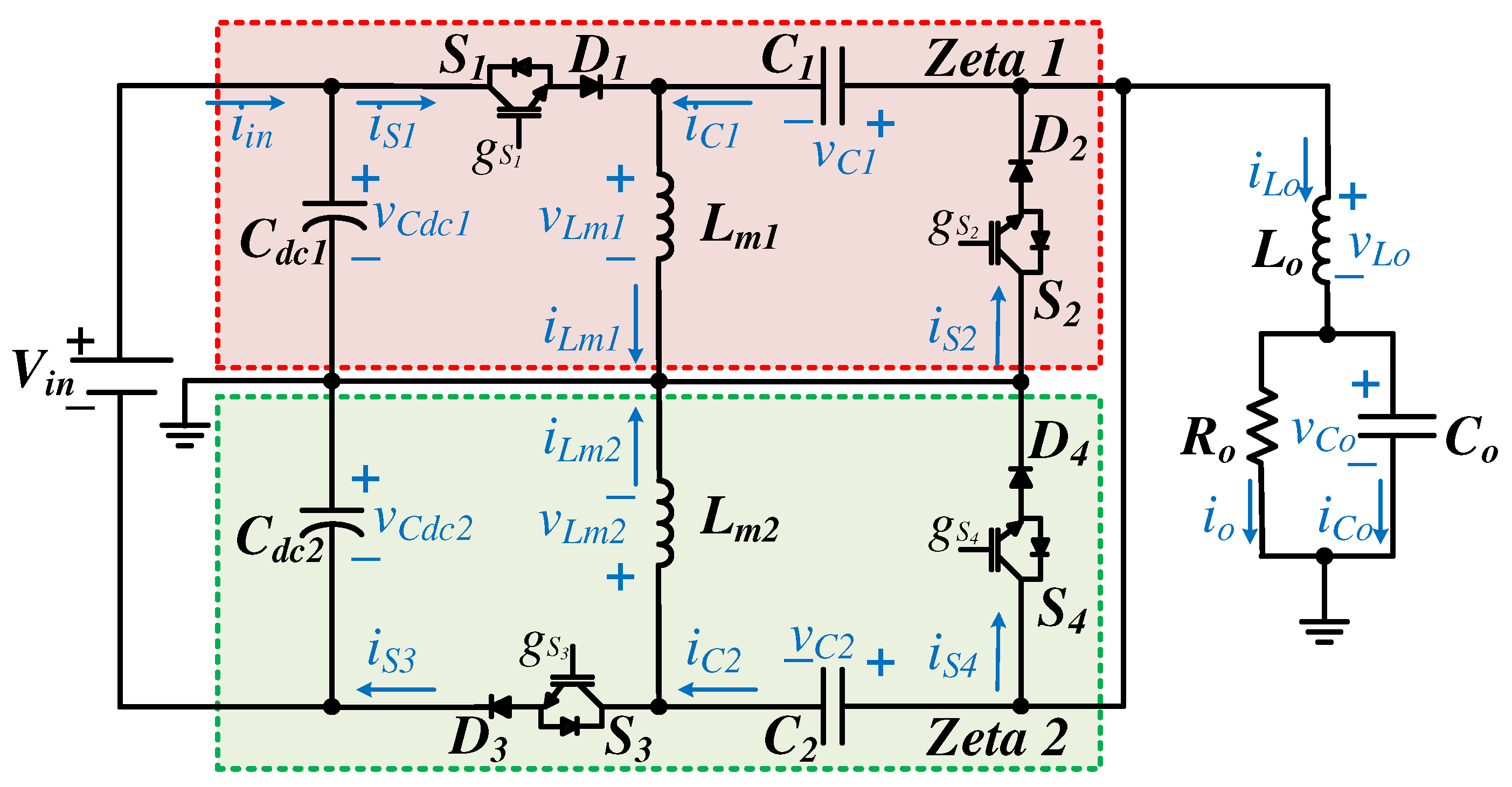
This paper aims to contribute to the scenario of renewable energy by proposing a novel low-power integrated inverter based on the Zeta converter, named single-phase integrated Zeta inverter (SP-IZI). The converter is composed of four switches, two of which operate at high frequency, while the other two operate at low frequency, more specifically at the frequency of the output voltage. In this paper, the converter is presented to operate as a sinusoidal voltage source in standalone mode, which is helpful in supplying local loads from a DC voltage source, such as a PV array or a battery.
This converter is the evolution of Zeta-based integrated inverters. In [
15], the converter operates as a current source, injecting energy into the grid and into the discontinuous conduction mode (DCM). However, this integrated inverter employs series diodes connected to the input inductors, leading the system to present high voltages on the power switches, limiting the overall system operation. In [
16], the converter was modified to solve this problem. However, the converter also operates in the DCM and is grid-tied as a current source.
The Zeta-based integrated inverter was also presented in [
17], operating as a standalone sinusoidal voltage source for autonomous GD/battery systems. However, the operation in the DCM can be represented by less complex and challenging mathematical models from the point of view of the output voltage controller. However, using the converter in the CCM for the same power level reduces the RMS value of the currents in the power switches and diodes, which indicates a more efficient operation once the elevated RMS currents are related to conduction losses. Nonetheless, this article proposes the SP-IZI converter operating in the CCM, making it more efficient than previous proposals [
15,
16,
17] and able to operate as a sinusoidal voltage source for local loads. At the same time, the proposed controller overcomes the difficulties in controlling the output voltage without the need to measure the output inductor current.
The SP-IZI topology proposed in this paper also presents some advantages when compared to [
10,
11,
14], such as: (i) fewer switching devices and gate drivers; (ii) reduced costs by using fewer switching/gate-driver devices; and (iii) the use of a high-frequency transformer is not necessary for the system operation. Therefore, as the proposed SP-IZI employs unidirectional power switches, the inverter works with characteristics similar to those of the traditional Zeta converter.
Given the phase margin characteristics of the Zeta converter transfer function, the sinusoidal output voltage was controlled using a proportional–integrative multi-resonant controller. Thus, obtaining output voltage with low total harmonic distortion (THD) was possible even when operating with a non-linear load. The complete analysis, performance, efficiency, and development of the proposed SP-IZI are evaluated and validated via the experimental results.
This paper is organized as follows:
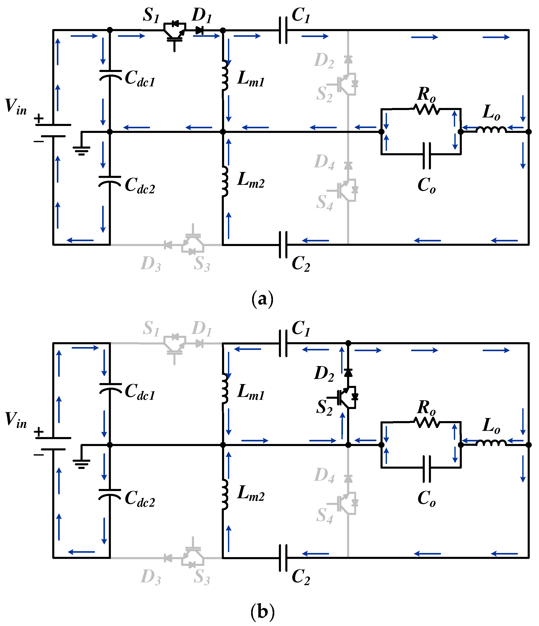
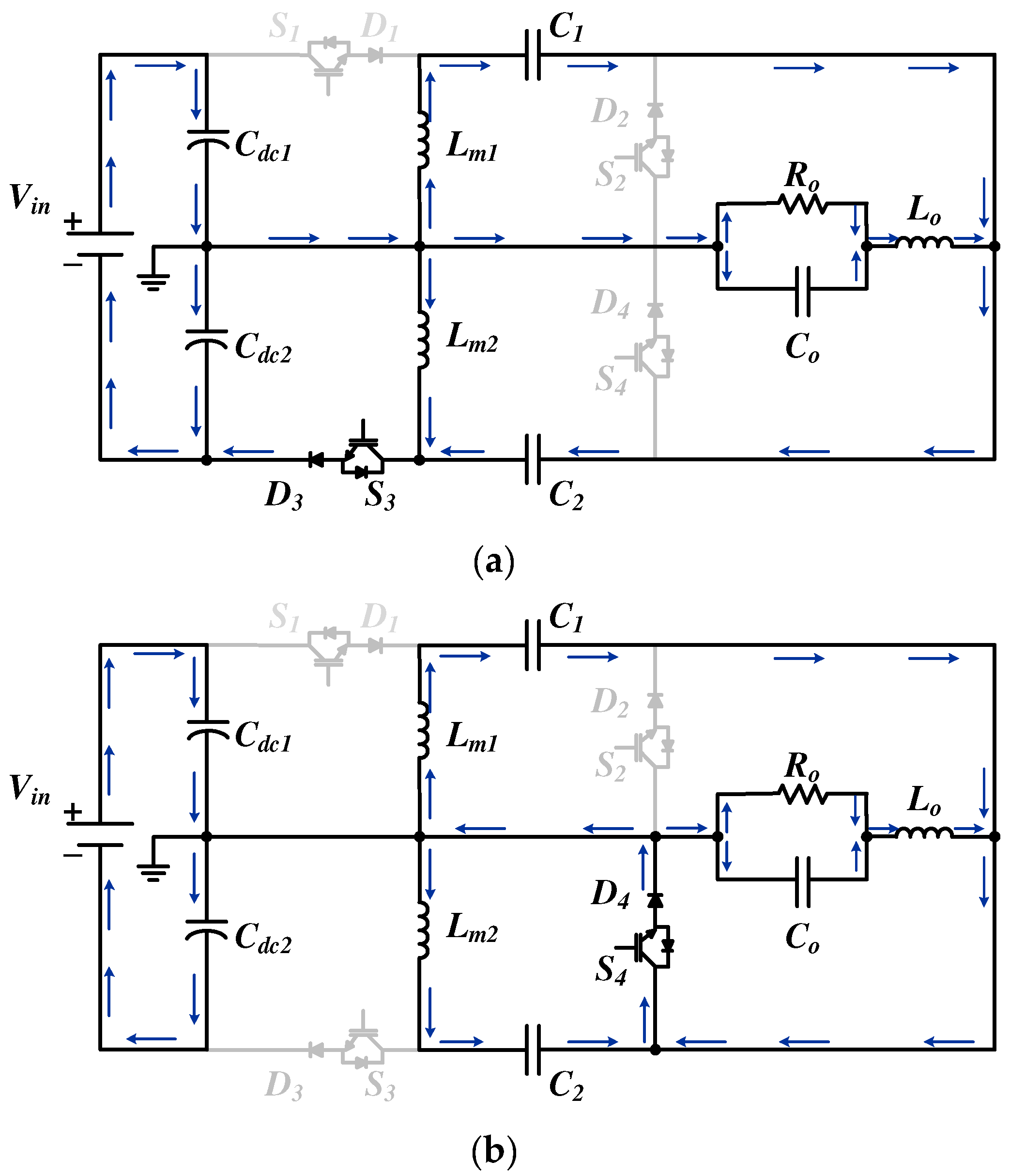
Section 2 describes the SP-IZI topology and its operation in CCM, while
Section 3 presents the switching logic and the mathematical modeling of the converter and the voltage controller.
Section 4 presents and discusses the experimental results, and
Section 5 presents the conclusions.
3. Output Voltage Control of SP-IZI
The SP-IZI operates with two high-frequency and two low-frequency power switches. Thus,
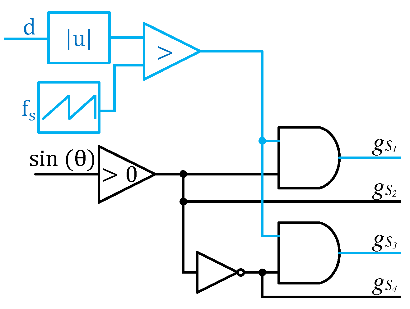
Figure 4 presents a block diagram of the proposed converter’s switching logic. As can be seen, the decision criterion for defining the switches and, consequently, the converter in operation is the sign of output voltage reference signal. This sinusoidal signal is self-generated and has 60 Hz. When it operates in its positive half-cycle, the Zeta 1 converter switches (see
Figure 1) are in operation. When the output voltage reference is negative, the Zeta 2 converter switches operate. In this way, the low-frequency switches operate at the output voltage frequency. On the other hand, high-frequency switches are driven by a PWM modulator, with modulating signal
generated by the controller. Finally, this control signal
is rectified before being compared with the sawtooth-shaped carrier.
In this paper, the SP-IZI is controlled to operate as an AC single-phase voltage source, delivering an AC-regulated voltage to the load. The mathematical model that represents the output voltage
from the duty-cycle
was achieved from the SP-IZI equivalent circuit, which can be obtained considering that both Zeta-modified converters operate symmetrically. The high-frequency equivalent circuit of the SP-IZI converter is shown in
Figure 5. It is important to highlight that the low-frequency switches are disregarded. This circuit considers the equivalent inductance
and capacitance
.
From this circuit, it is possible to obtain the differential equations representing the circuits formed in the two operation stages. All the elements were considered as ideal. When the high-frequency switch is turned on, the equations for the derivatives of states are presented below:
On the other hand, when the high-frequency switch is turned off, the diode is forward-biased. Thus, the equations for the derivatives of states are shown below.
The small-signal modeling technique [
18] was applied to obtain the small-signal model of the converter. The variables in capital letters are the values calculated in the nominal operation point of the converter. In this analysis,
is the complementary value of the nominal duty-cycle
, calculated as
.
From the state-space model (3), it is possible to obtain the small signal transfer function of the output voltage
from the duty-cycle
by applying it in (4) [
19]:
where
is the Laplace variable and
is an identity matrix with the dimension of
.
Thus, in terms of the converter parameters, the transfer function
is presented below.
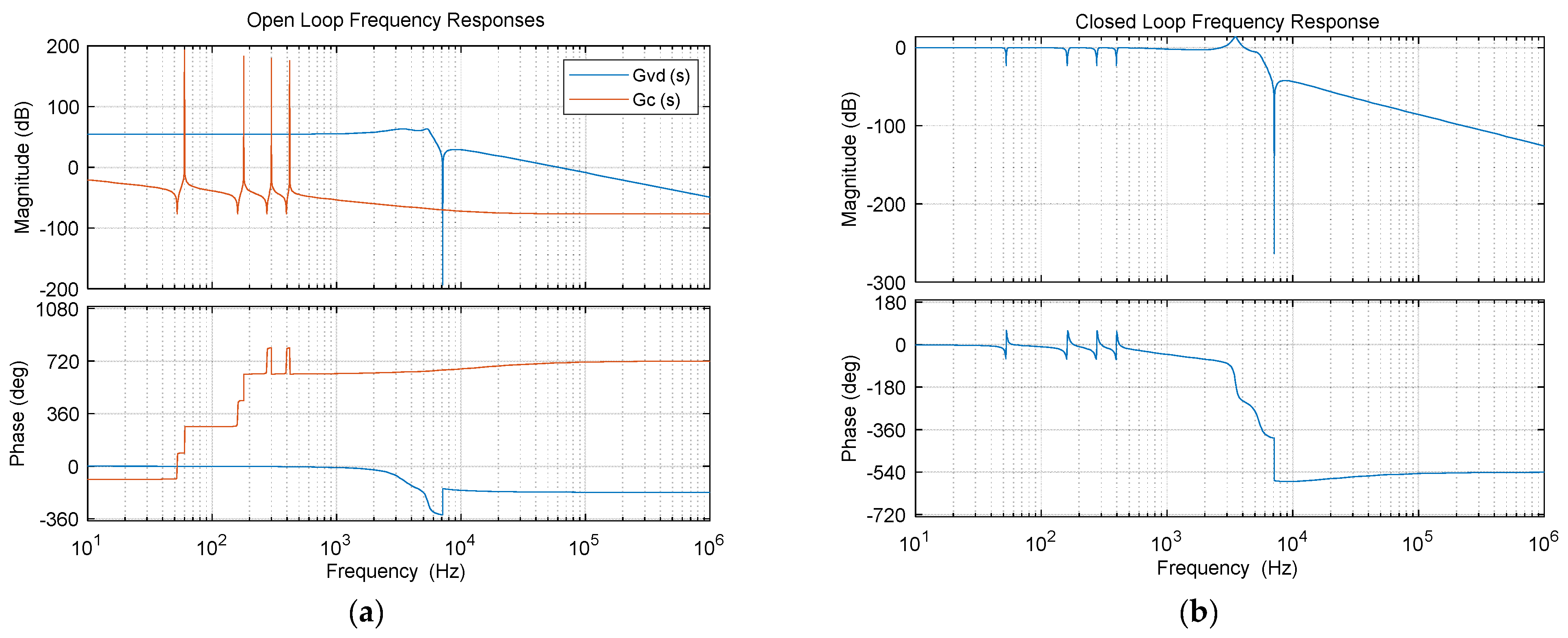
Considering the converter parameters presented in
Table 1, the transfer function’s open loop frequency response is presented in
Figure 6a. As can be seen, there is a range at low frequencies in which the system can be controlled with a proportional–integral (PI) controller since the open-loop phase of the system is between
and
[
20]. Therefore, a PI voltage controller was used to ensure adequate settling time during transients and the rejections of harmonic components over a wide range of frequencies. On the other hand, the PI controller cannot provide a null steady-state error for sinusoidal references, or even the complete rejection of harmonic disturbances caused by non-linear load currents. Thus, a first-, third-, fifth-, or seventh-order multi-resonant (MR) controller was added in parallel to the PI controller, yielding a PI-MR controller [
21]. The controller transfer function
is presented below.
The PI controller was designed with specifications of a 0 dB crossover frequency
and a phase margin of
. The gains were obtained with the methodology presented in [
20]. The design specifications and gains of the controllers are presented in
Table 1.
Figure 6a presents the controller’s open-loop frequency response. In the 0 dB crossover frequency
, the controller’s gain compensates for the gain of the open loop system. At the same time, at resonant frequencies, the controllers guarantee gains tending to infinity. Thus, as shown in the closed-loop frequency response presented in
Figure 6b, the system is stable and presents gains and phases equal to zero at the resonance frequencies. At the same time, there is a wide passband with the gain close to 0 dB and a small phase delay, indicating that the PI controller acts at frequencies with no tuned resonant controllers.
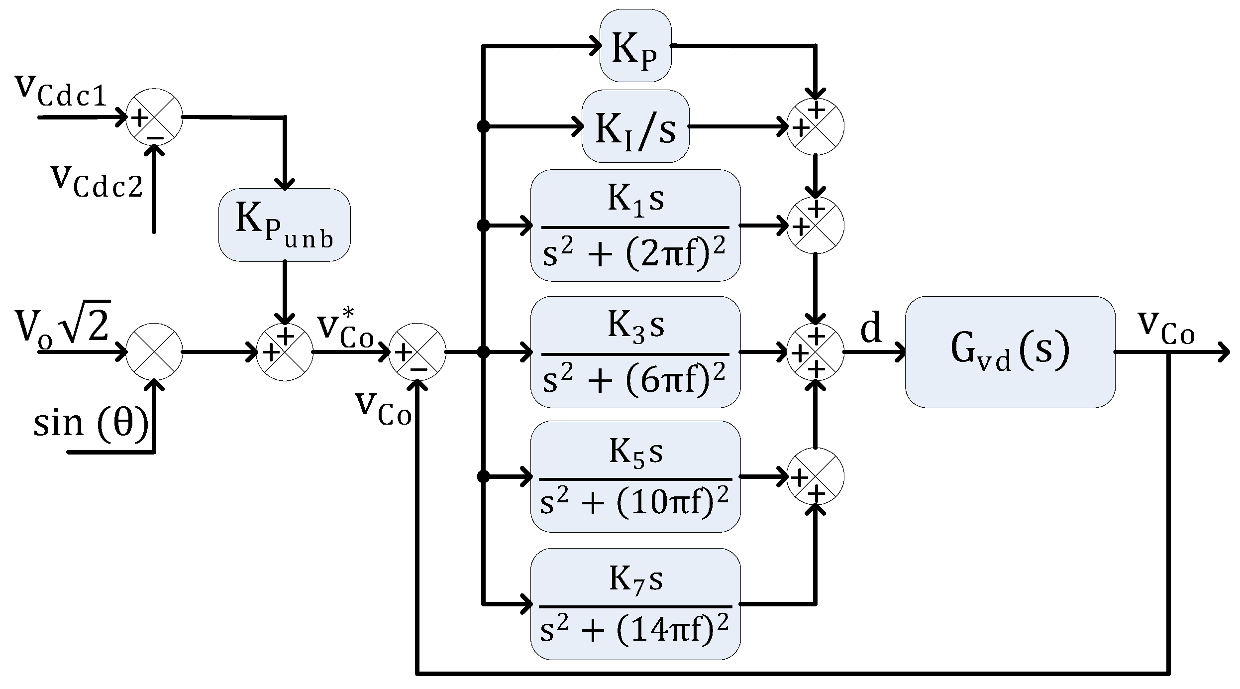
The block diagram of the control system is presented in
Figure 7. As can be seen, the output reference voltage signal is obtained with a self-generated sinusoidal wave with the desired output frequency. Furthermore, the SP-IZI presents a split-capacitor structure in its DC-link. Thus, it is necessary to implement a voltage unbalance controller to prevent the DC-link capacitor voltages from diverging [
22]. We implemented a proportional controller with unitary gain
.
4. Experimental Results
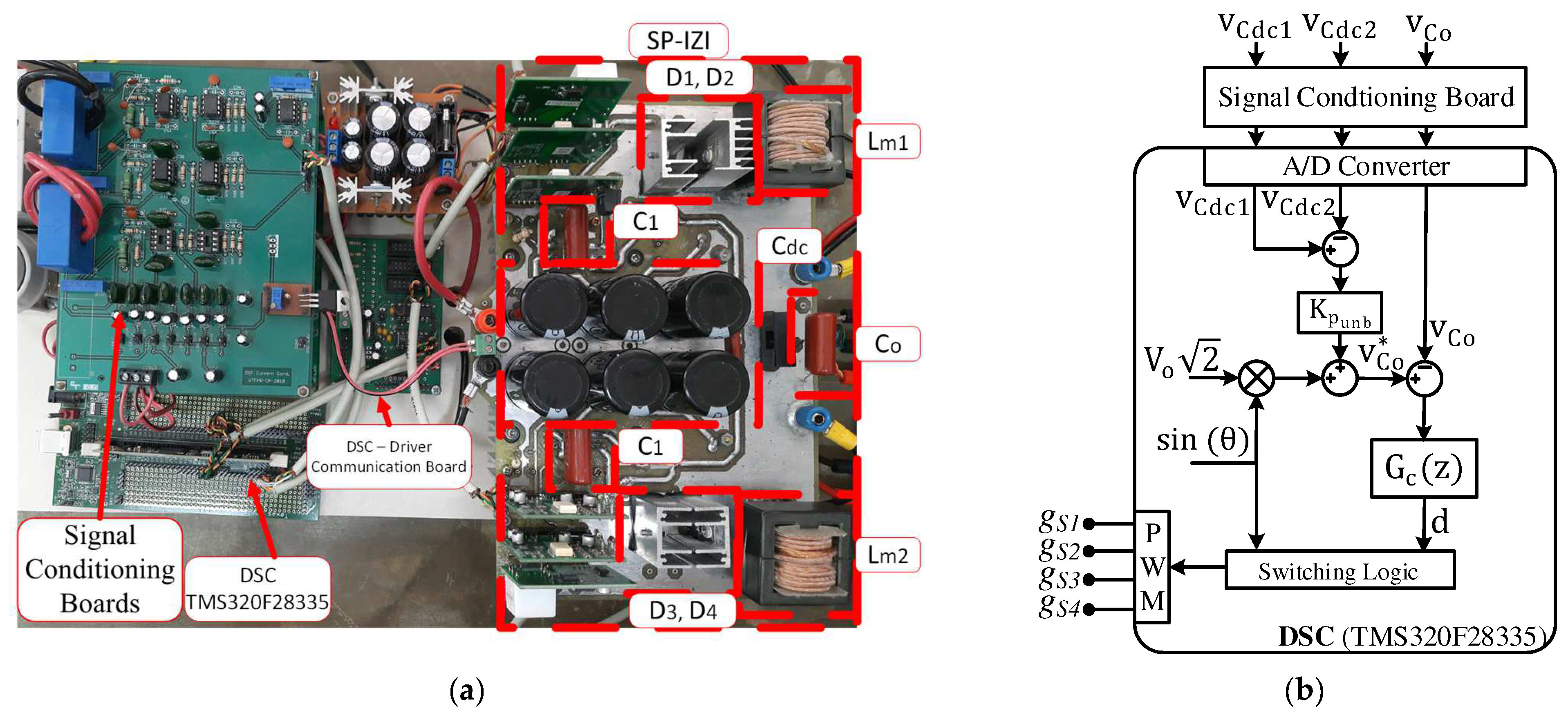
A 324 W prototype was developed to experimentally evaluate the proposed SP-IZI, as shown in
Figure 8a. The power switches were placed under the printed circuit board and could not be visualized. The experimental setup was deployed using discrete CoolMOS switches IPW65R037C6 (Infineon, Neubiberg, Germany) and SiC Schottky diodes FFSP2065B-F085 (OnSemi, Poenix, AZ, USA). It is important to highlight that it is a modular prototype, helpful in evaluating some other topologies. Thus, the conditioning signal system has more components than the SP-IZI control system. The block diagram of the control system implemented in discrete time is presented in
Figure 8b. The voltage and current quantities were measured using LEM transducers, and the signals were conditioned by specific conditioning boards. All the controllers and algorithms were embedded into the digital signal controller TMS320F28335 (Texas Instruments, Dallas, TX, USA), and the output voltage controller was discretized using the Tustin method. The power quality indexes and system efficiency were measured by Fluke 43B and Yokogawa WT3000, respectively, while the waveforms were collected with a digital oscilloscope 190 series II (Fluke, Everett, WA, USA). The main SP-IZI parameters employed for building the experimental tests are presented in
Table 1.
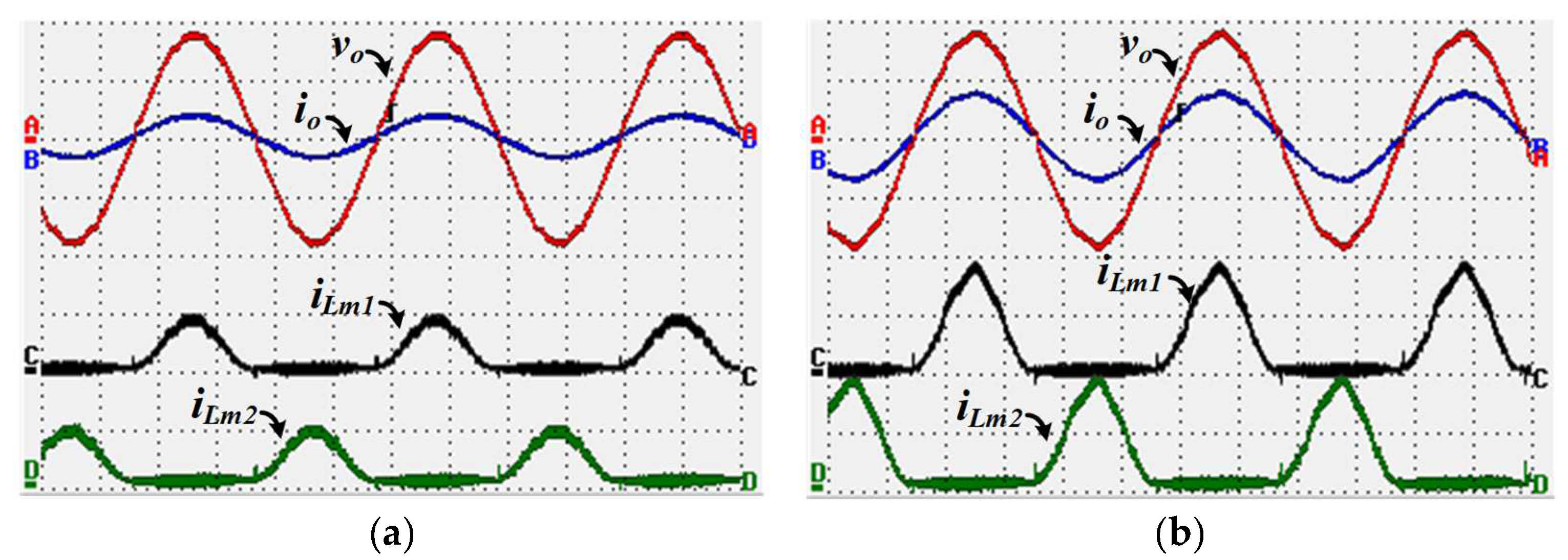
The topology was evaluated experimentally under several static conditions, considering resistive loads. This paper shows the waveforms of the tests with the resistive loads of 162 W and 324 W, as well as a test with a resistive load of 162 W in parallel with a single-phase rectifier followed by an RC Load (200 Ω and 100 μF), forming a non-linear load.
Figure 9 presents the experimental results obtained for the resistive loads mentioned above, in which the voltage and current supplied to the load are shown in conjunction with the currents of the inductors
and
. As demonstrated in
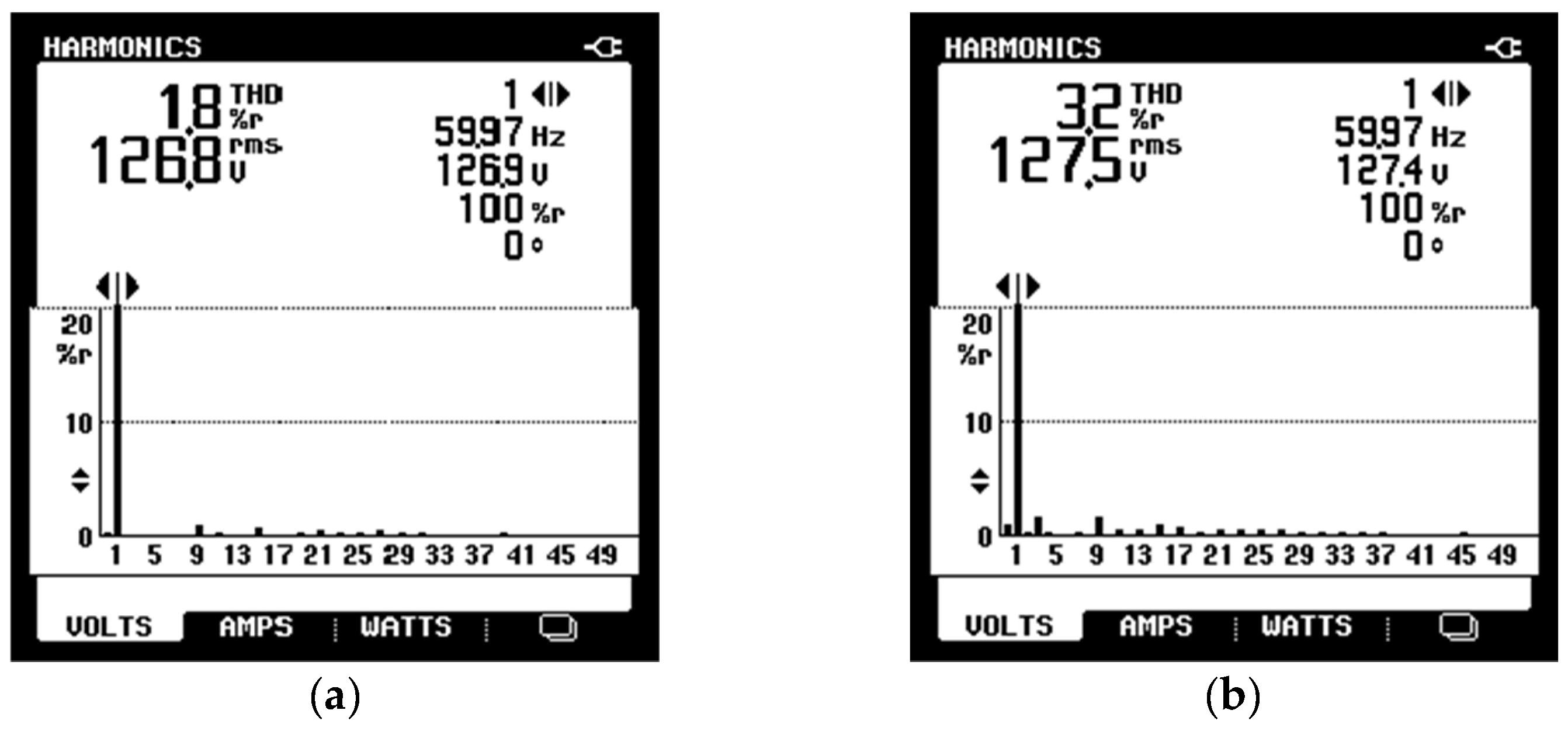
Figure 9, the SP-IZI delivers a sinusoidal voltage to the loads in both conditions. The frequency spectra of the voltages supplied to the loads are shown in
Figure 10. As can be seen, the output voltages are regulated and present low THD. At the same time, it is important to highlight that the main harmonic components that compose the voltage are at frequencies with no resonant controllers.
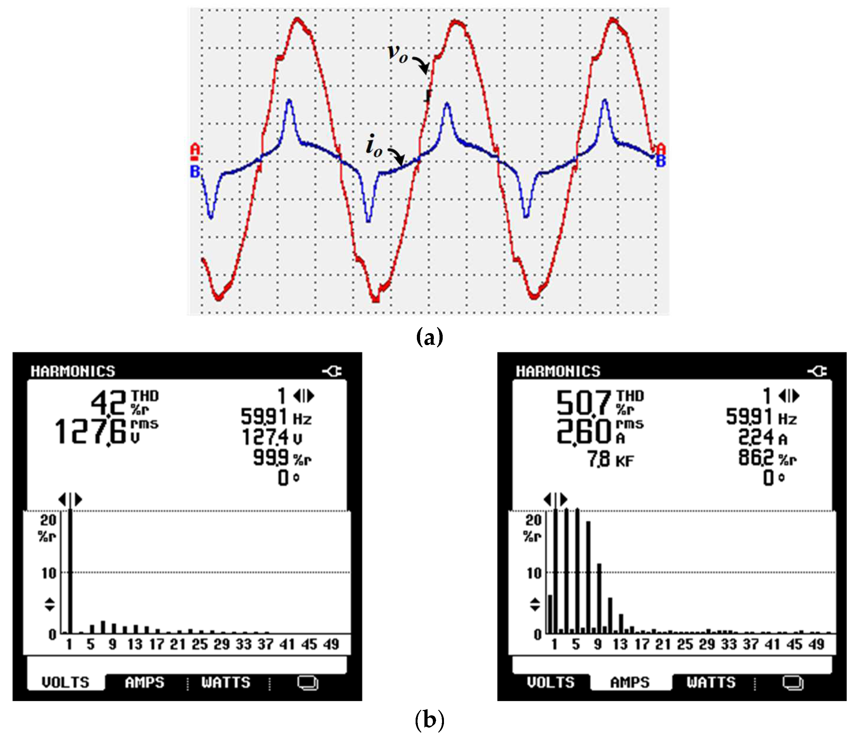
Figure 11a shows the waveforms of the output voltage and current considering the non-linear load. At the same time, the frequency spectra of these variables are shown in
Figure 11b. As can be seen, the current drained by the load has a THD = 50.7%. On the other hand, the output voltage controlled by the SP-IZI reached THD = 4.2%, meeting the main power quality standards [
23,
24].
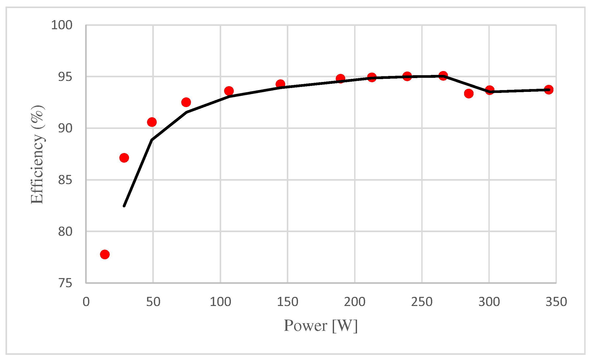
The efficiency of the SP-IZI operating in the CCM and as a sinusoidal voltage source was evaluated experimentally by varying the resistive load.
Figure 12 shows a graph of the efficiency measured from the resistive load power. As can be observed, the efficiency is near 95% in a wide range of operation points. Thus, the SP-IZI is a suitable inverter for replacing the conventional cascade association of the DC/DC step-up converter with the voltage source inverter.
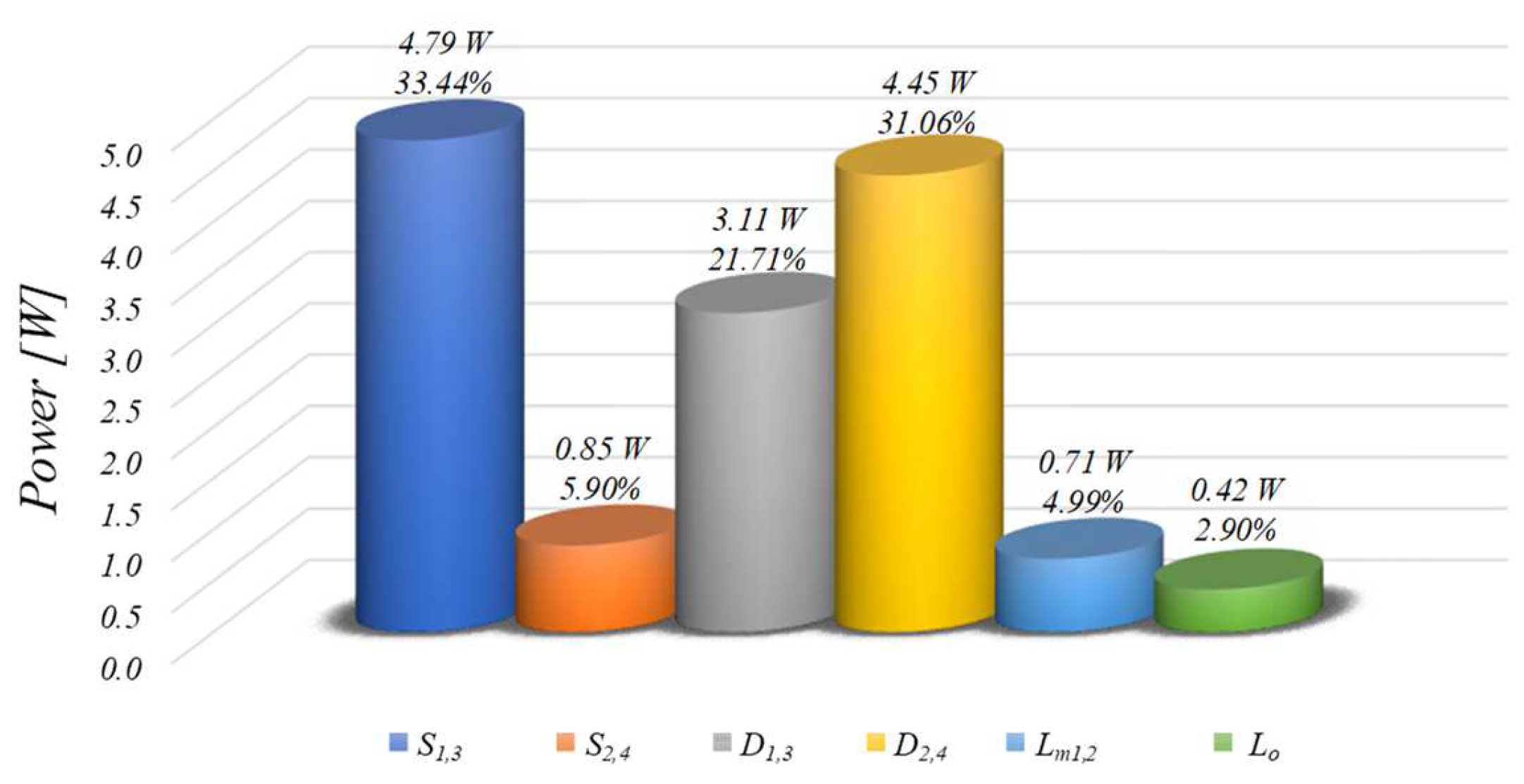
Figure 13 shows the losses in each element of the converter and their percentage value concerning the whole, with the integrated inverter operating at nominal power. The values were obtained by measuring the currents and voltages of the elements in computational simulations and applying them to the specifications determined in the datasheets of the power switches and diodes.
As can be seen, around 33% of the losses are associated with the high-frequency switches and , where 3.18 W is related to conduction losses and 1.61 W is related to the commutation losses. In the diodes and , which are complementary to high-frequency switches, the losses represent 31%, divided into 2.35 W for conduction losses and 2.10 W for switching losses. In addition, the diodes placed in series with the high-frequency switches ( and ) are responsible for 21% of the overall losses. On the other hand, it is possible to verify that the losses associated with the low-frequency switches represent less than 6% of the losses, mainly related to conduction losses. Finally, all inductors’ core and windings losses correspond to less than 8% of the overall losses.
Table 2 summarizes a comparative analysis between the SP-IZI and the main similar inverters available in the literature, considering the number of devices in each topology and its efficiency, focusing on topologies that operate with low voltages in their inputs. As can be seen, the topologies [
7,
14,
25,
26] that obtain an efficiency greater than or equal to 96% have more power switches than the proposed topology. On the other hand, the topology [
27] has the same number of switches and fewer inductors and diodes. However, its efficiency is limited to 94%.
From an implementation cost perspective, the inverters use distinct quantities of active and passive components, which generate different costs. In this way, a direct cost comparison may be unrepresentative. However, some similarities are found when analyzing the models of switches and diodes used in the converter presented in
Table 2.
This paper and the topologies proposed in [
7,
25,
26,
27] employ switches around 600–650 V and a maximum collector current between 40 and 53.5 A. The topology proposed in [
25] uses a high-speed IGBT with a fast and soft recovery antiparallel diode presenting 650 V of breakdown and a maximum collector current of 53.5 A. This IGBT is enough for the mentioned works, and was considered in the cost comparison of these topologies. In [
26], distinct switches were considered, with 150 V as the maximum voltage and 50 A as the maximum current. The other one presents 650 V and 11 A maximum voltage and current, respectively, totaled for the six switches in this topology. Finally, [
14] uses switches of 1200 V and 40 A maximum.
Those used in SP-IZI and [
27] are similar as regards their diodes. However, [
27] uses diodes that tolerate 650 V and 30 A, while the diodes in this paper present the maximum as 650 V and 20 A. Thus, the diode used in [
27] is adopted for the cost comparison. Additionally,
Table 3 also includes costs related to capacitors and inductors. The costs involving capacitors are estimated based on the capacitance and application, i.e., whether it is a coupling capacitor or used in the DC-link.
On the other hand, the costs for the inductors consider the inductance. Generally, an inductor with elevated inductance needs a bulkier core and windings, increasing costs.
Table 3 summarizes the main costs and exhibits the values per unit (pu).
Concerning the topology proposed in [
7], which obtains slightly higher efficiency and slightly lower cost than the proposed SP-IZI, it is necessary to consider that such a topology uses twice as many power switches as the topology proposed in this paper. Thus, the number of components required to drive all the power switches, as well as the largest capacity required from the microcontroller to activate it, also need to be bigger. At the same time, the output voltage of this converter is composed of many high-frequency components. Thus, considering
Table 2 and
Table 3, it can be concluded that the SP-IZI integrated converter is an option that has good efficiency ratio for the number of active and passive components.
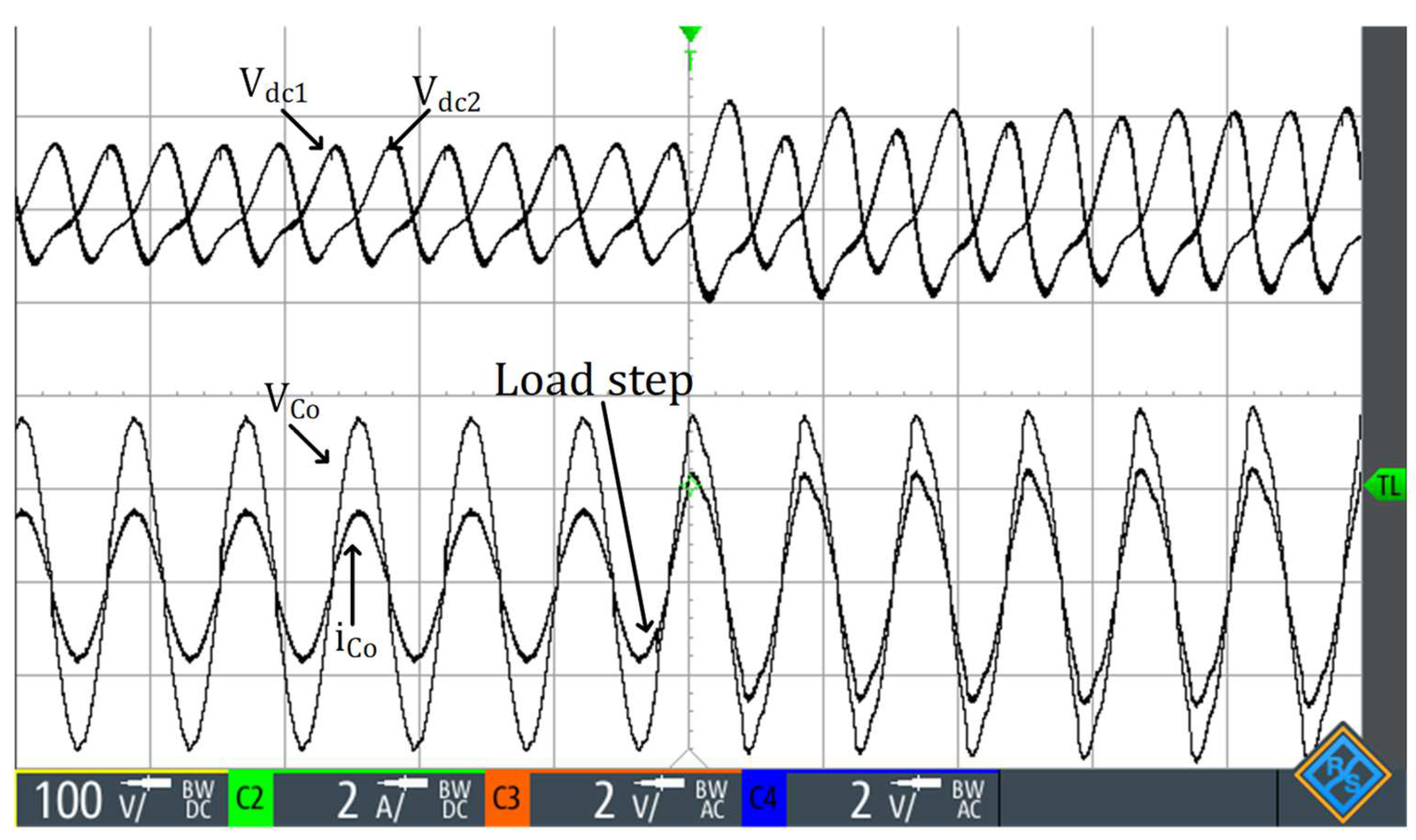
Finally, the experimental dynamic result is presented in
Figure 14, with a 70 W power load step (140 W to 210 W). As can be seen, the output voltage presents as transient when the load is connected. However, there is no discernible long-term transient.
Figure 14 also shows the voltages
and
of the DC-link capacitors. As can be seen, as a characteristic of a split-capacitor DC-link inverter, the voltages
and
oscillate at the output frequency [
28]. It is also possible to verify that the voltages are balanced, indicating the operation of the voltage-unbalance controller with zero error in a steady state.
5. Conclusions
This paper has proposed a new integrated inverter (SP-IZI) for grid-isolated applications, combining two modified Zeta converters to replace the traditional two-stage converter system, in which a step-up DC-DC converter was associated with a voltage source inverter.
The proposed integrated inverter has been detailed by presenting and analyzing its topological states. Although it has four power switches, two operate at the output voltage frequency, which facilitates analysis and switching logic, in addition to reducing switching losses. Then, the converter was mathematically modeled from its equivalent model, and a proportional–integrative plus a multi-resonant controller was designed and used to control the output voltage without the need to measure the output inductor current.
Static and dynamic experimental results have been presented to evaluate the feasibility of the proposed SP-IZI. The inverter provided sinusoidal voltage with a low THD for linear and non-linear loads. At the same time, data were presented on the converter’s efficiency at various load powers. The converter achieved close to 95% efficiency with a wide range of powers. A comparative study on the implementation cost of the converter proposed in this article and the main topologies proposed in the literature is also presented, from which it has been possible to conclude that the proposed converter obtains good ratios between implementation cost, efficiency, and number of components. Finally, the dynamic results demonstrate that the employed controller was effective, since it was stable and achieved an adequate establishment time in response to load variations.
