1. Introduction
The progress in power-electronics applications and the expanding range of power-electronics converters have significantly improved their operational capabilities in the field. Therefore, there is a substantial need to simulate and test these converters. Nevertheless, the necessity to build the converter and conduct physical testing on both the converter and its controller is reduced, due to many practical limitations. These limitations contain possible hazards of harm, doubts about the robustness of the converter, and the associated financial costs. Real-time simulation (RTS) is a common way to test how well a converter controller works in a hardware-in-the-loop-(HIL) environment, which involves connecting actual physical components to simulated models. Incorporating real-world hardware effects into this integration improves the dependability of the simulation, rendering it a viable instrument for validating control techniques and evaluating the efficiency of power-electronics converters, which gives RTS an advantage over other simulation methods, in regard to accuracy and reliability [
1,
2].
Prior to installation and commissioning, it is necessary to conduct testing and verification procedures on the controller, to ensure its functionality. Performing testing in a real-time-simulation-(RTS)-environment setting is the most feasible approach to guaranteeing the system’s resiliency and to effectively evaluating its capabilities and functionality. Moreover, utilising RTS is vital for executing random switching investigations, as it substantially reduces the total length of the study. RTS is renowned for its capacity to deliver instantaneous reactions, enabling the dynamic simulation of power-electronics systems with precise timing data. RTS provides a more accurate depiction of the system’s dynamic reaction compared to conventional time-domain simulations, which may not accurately replicate real-time behaviour [
3,
4].
In order to examine the dynamics of any given system, the simulation speed must fall within the range of tens of seconds. The process that is being referred to is commonly known as real-time simulation. The real-time simulator effectively solves the mathematical model of a given system by discretising time into short and defined steps. It then correctly reproduces the desired waveforms, such as the voltage and currents of power converters. Enhanced mathematical models yield heightened precision in voltage and current measurements. The slowness of the simulation time observed in power converters can be attributed to the inefficient switching technique employed by these devices. Furthermore, the model needs to include the capability of observing switching characteristics and detecting and analysing unusual events, such as switch short circuits. Additionally, the model must account for the latency in data transmission from the converter switches and external networks, resulting in errors. Hence, developing a stable model for switching converters featuring many topologies is a great challenge.
A flexible numerical integration method is one approach to accurately and efficiently modelling converters. This method allows for the appropriate level of speed and precision in the modelling process. Additionally, interpolation techniques can be employed to correct errors arising from the switching phenomena. It is important to note that this approach does not fix the simulation time step and nodal matrix. Furthermore, the solution method is characterised by its non-iterative nature. If many switching-device models require changes in status within a single time step, the network model is accordingly adjusted to accommodate all of these demands. The last ones are only considered in the resolution of the subsequent time interval. Hence, the solution is deemed inaccurate for a fraction of the time-step size after the first request. This inaccuracy can lead to the development of switching errors, inaccurate power flows, and non-characteristic harmonics. The measures implemented to mitigate the associated inaccuracy often entail modifications to the time-step size and the utilisation of interpolation algorithms. Therefore, a notable drawback to these approaches is the substantially higher levels of computing effort at specific time intervals. This conflicts with the real-time simulation, as it demands that the solution process be efficient in each time step [
5].
Another approach to RTS modelling is the resistive model. While this method enhances the system’s dynamic behaviour by eliminating undesirable oscillations, it also requires changing the system’s topology for each switch state. This presents a significant challenge when dealing with complex and large-scale systems. However, in the case of basic converter types, it is possible to utilise a resistive model to obtain a speed advantage at the expense of accuracy. By contrast, it is observed that nonlinear switch models exhibit significant inefficiency when employed for CPU simulation. Moreover, their implementation on FPGA platforms generally requires a significant allocation of hardware resources, primarily due to the iterative nature of the solution. The time-averaging method and the state-space method (SSM) are alternative approaches that can also be employed. The accuracy of the SSM approach to solving equations is limited, particularly when verifying the controller linked to the switching power converter. The asynchronous interface between the controller and the simulator poses a significant challenge in this regard [
6,
7].
The utilisation of the ADC technique has various advantages. Firstly, the stability of the network matrix is defined, making it constant and stable, hence avoiding the need for matrix inversion calculations, leading to less computational burden and higher computational efficiency [
2]. Furthermore, the utilisation of field-programmable gate arrays (FPGAs) can lead to enhanced efficiency, hence reducing the amount of memory space consumed within the FPGA. However, the ADC model generates simulation losses and transients not present in real-world scenarios. Numerical errors are considered to be the inaccuracies that arise from the ADC-based model [
4,
8].
The next parts of this paper are structured in the following manner.
Section 2 provides a comprehensive overview of the modelling process using the ADC method.
Section 3 gives the eigenvalues analysis used to select the optimal ADC parameters.
Section 4 outlines the proposed approach for the optimal calculation using the ABC, GA, and FF algorithms. The simulation results obtained through the utilisation of the proposed method are presented in
Section 5. Subsequently, the conclusion of the study is outlined in
Section 6.
2. Associated-Discrete-Circuit-(ADC) Modelling
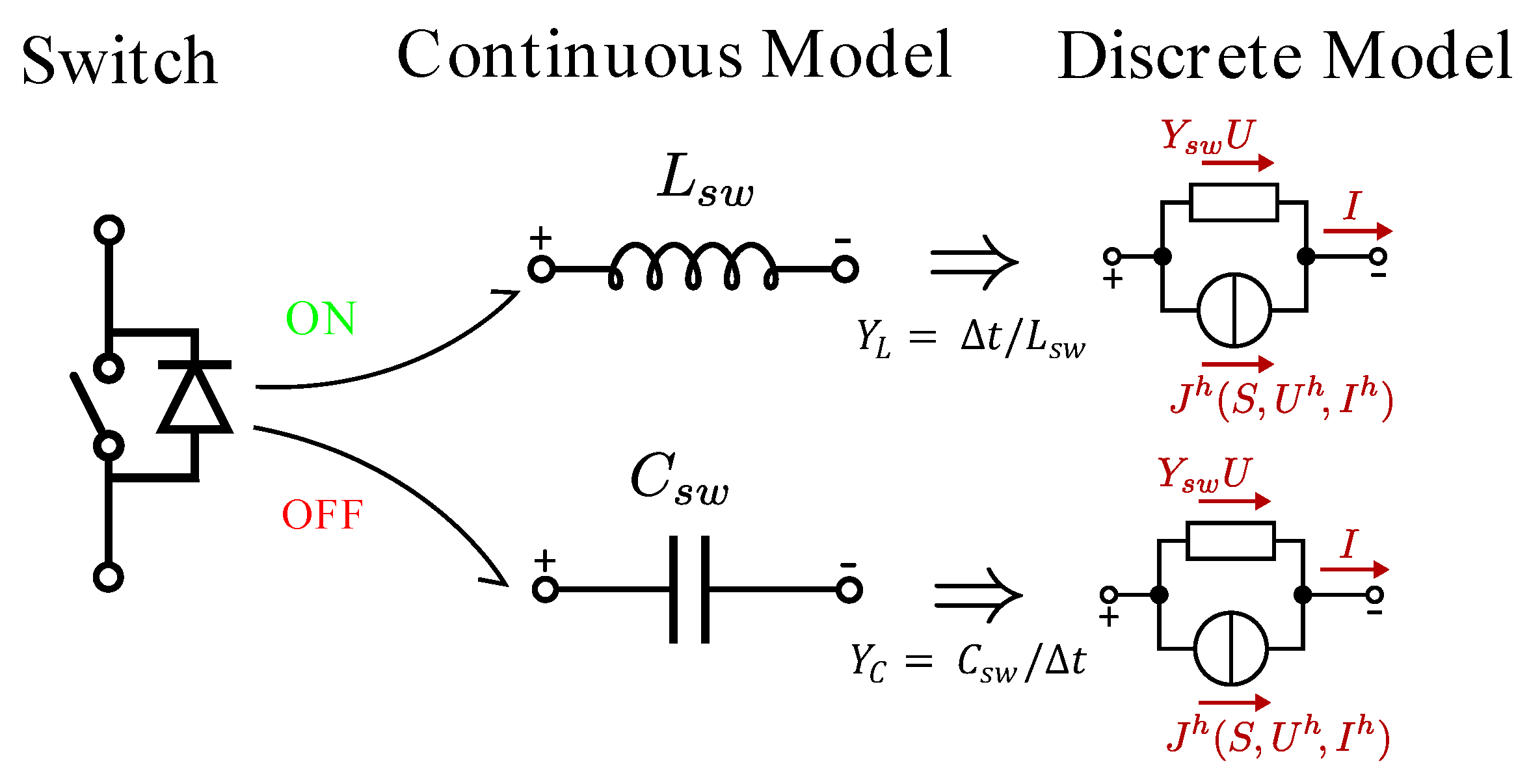
The associated-discrete-simulation method integrates a model representing an equivalent conductance and a current source. The mentioned parts are connected in a parallel configuration, to effectively replicate the operational characteristics of the various switching elements within the circuit, including but not limited to IGBTs, diodes, thyristors, and related devices, as shown in
Figure 1. The inductive characteristics of the power switch are observed while it is in the ON state, and these characteristics can be measured using the parameter
. On the other hand, during the OFF state, the power switch demonstrates capacitive characteristics, which can be symbolised by the variable
. A small parasitic component can be integrated into the model, to mitigate the presence of overshoots and oscillations in switching transients. One such element is a resistor denoted as
, which can be connected in series with the capacitor
. The optimal operation of these models requires the usage of low capacitance and inductance values. As a result, this enables a reduction in the required time interval, denoted as
, to develop the discrete-time system. Hence, this specific model is sometimes referred to as the small-time-step model in academic literature [
9,
10].
The discrete-time model of the ADC switch in the ON state can be represented as
The earlier calculated inductor current, labelled , can be considered a continuous current source, represented as . Moreover, the parallel conductance, represented as , determines the increase in current caused by the voltage U during the given time step.
Equations (
3)–(
5) represent the discrete-time model of the ADC switch in the OFF state, assuming we neglect the extra damping resistance. The variable
represents the voltage magnitude at the preceding time step. The variable
denotes the conductance of the switch in its inactive state:
Rearranging Equation (
3) by expressing the current
I, Equation (
4) is formulated:
where
The position of the switch, represented as
S, solely impacts the current source, while the conductance stays unaltered by the switch position. Therefore, the equation governing the behaviour of the switch can be formulated as follows:
The logical role of the switch state
S in the context of an IGBT switch with a parallel diode is as follows:
The variable
G is utilised to indicate the turning-on signal for the power switch, such as an IGBT. The other parts in Equation (
7) describe the condition of the diode. Different varieties of power switches necessitate an alternative form of logical operation. It is essential to acknowledge that, in contrast to other behavioural models of power converters, the logic functions in ADC models are specifically designed to address the switching devices on a local level without considering the overall circuit logic.
However, it is important to acknowledge that the capacitors and inductors acquired via the ADC method may not precisely reflect the parasitic components in real switches. The presence of this gap presents the ability to introduce inaccuracies inside the simulation. In the domain of transient functions, there have been notable numerical simulation mistakes when applying the ADC modelling method. Switching power losses arising from numerical integration are acknowledged despite their absence in the physical domain. During modelling, it was noted in a prior work [
11] that switching losses occurred due to inaccuracies in circuit parameters. Nevertheless, a thorough examination of this occurrence still needs to be undertaken.
In Equation (
8), it is assumed that during the
n step, the switch is in the ON state. In that instance, the switch can be considered equivalent to the inductor (
), and it is possible to determine the amount of energy stored on the inductor. As a parallel current source represents the energy stored in the inductor:
In the
time step, the switch is in the OFF state,
is replaced by
, and the initial energy stored in the capacitor is calculated using Equation (
9). The energy stored in the inductance goes to zero in the ON-OFF state transition of the switch:
In Equation (
10), it is also assumed that during the
n step, the switch is in the OFF state. In that instance, the switch can be considered equivalent to the capacitor (
), and it is possible to determine the amount of energy stored in the capacitor:
Also, in the
time step, the switch is in the ON state,
is replaced by
, and the initial energy stored in the inductor is calculated using Equation (
11). The energy stored in the capacitor goes to zero in the OFF-ON state transition of the switch:
The capacitor will change to an inductor for a switch modelled using the ADC method to be switched to ON. The initial current flowing through the inductor must equal that of the capacitor, which is 0 amperes. There is no abrupt alteration in the flow of electric currents within the inductor. The charging process of the ADC switch commences, leading to a gradual rise in the current of the equivalent inductor until it achieves a steady state. Meanwhile, the voltage of the switch will gradually decline to zero. The multiplication of the voltage and current values of the ADC model yields a non-zero result. Similarly, the energy expended during this operation is also non-zero, which can be interpreted as the energy stored in the inductor.
The same can be noticed during the switch turn-off, as the model will change from an inductor to an equivalent capacitor. As the capacitor’s initial voltage and current are both zero, energy will be stored in the capacitor due to the charging process, as the capacitor voltage will reach a new non-zero steady-state value.
It is necessary to reset the current value of the inductor, in order to facilitate the subsequent switching-on operation, which aims to replace the capacitor with a state of zero current in a stable condition. In order to ensure proper functioning, it is necessary to reset the voltage value of the capacitor prior to replacing the inductor during the switching-off process. The phenomena above result in virtual switching losses inside the ADC model of a power switch.
Finally, the calculation of virtual power loss can be determined using the following equation:
To summarise, there are several drawbacks associated with this particular model. Firstly, the parameter settings are not universally applicable, and selecting an appropriate parameter set can often be challenging. The non-switching circuit components and the applied integration approach influence the transient behaviours. Additionally, in applications with high frequencies, the virtual power loss resulting from the charging and discharging of capacitors and inductors in the model can present challenges.
3. Eigenvalue Analysis for Optimum Switch Parameter Selection
The selection of the parameter value holds the capacity to influence the transient spikes introduced into the performance of the ADC model, as it directly represents the values of the switch inductance and capacitance. A non-optimized value of , for example, could result in a negative value, and the discrete-time system becomes unstable. To examine it, initially, the derivation of the state-space equation is undertaken. Additionally, it is necessary to convert continuous equations into discrete equations. In the end, the eigenvalues of the matrix representing the system are calculated. The determination of the optimal value of can be achieved by the analysis of the eigenvalues.
By utilizing continuous state space equations, where
A represents the state matrix and
B represents the input matrix, and by applying the Laplace transform and then working with the backward Euler technique, the substitution of
s by
in Equation (13) allows for the discretisation process:
This enables the formation of a relationship between the variables
z and
s, as indicated in Equation (
14). In this context,
represents the time step, whereas
s is the complex number
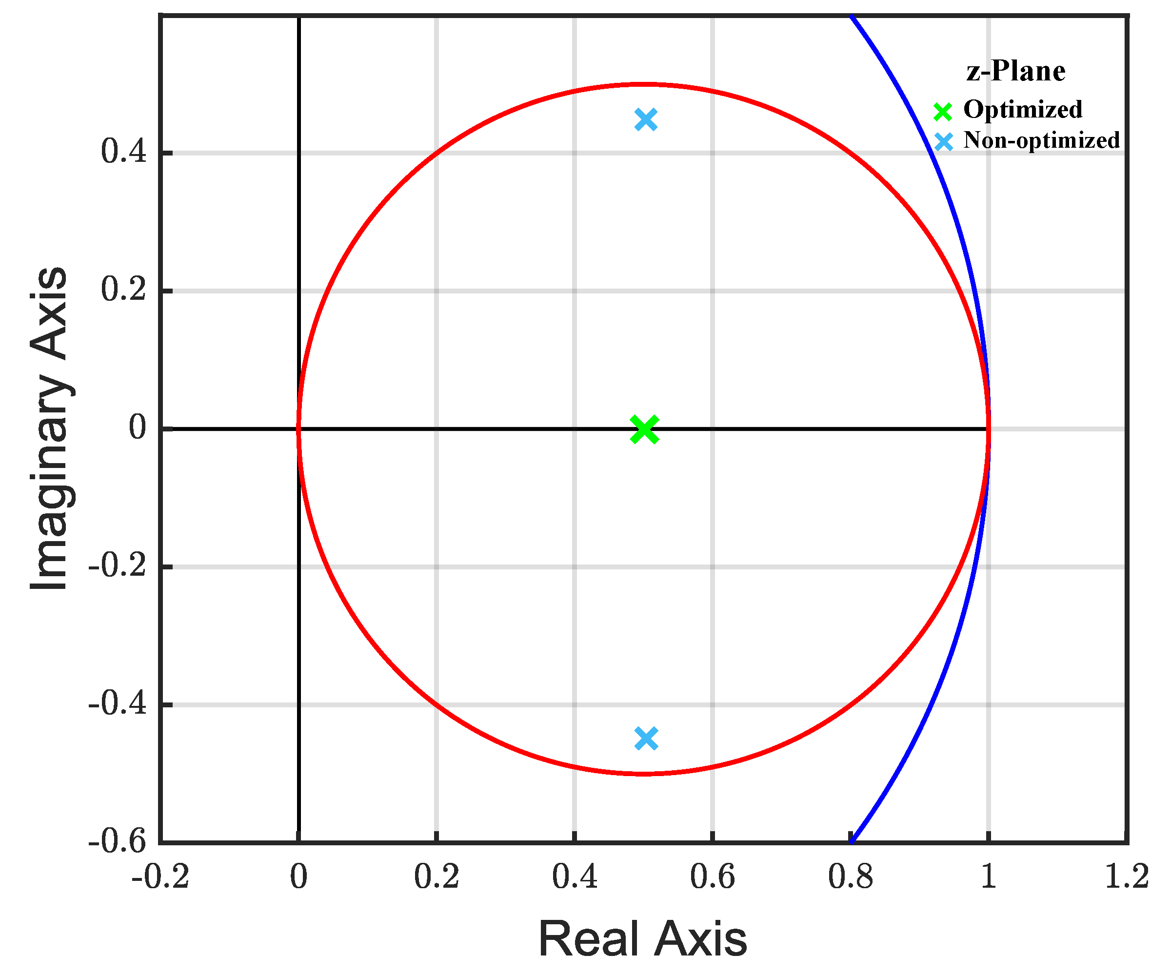
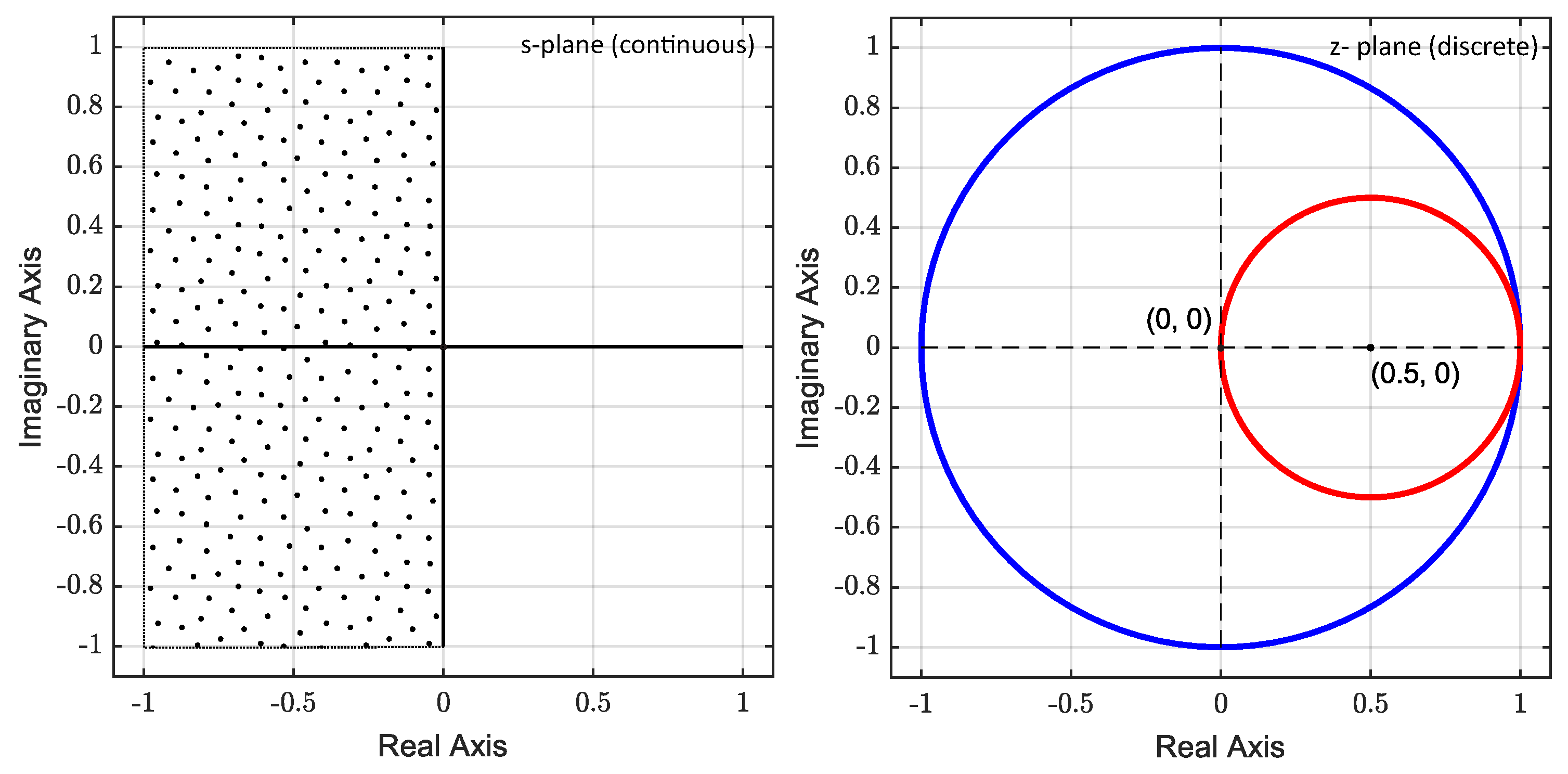
. By employing the backward Euler integration technique, it is possible to transform the left-hand side of the s-plane onto the z-plane, yielding a circular layout. The circle under consideration is the red circle, centred at the complex number
and has a radius of 0.5, as shown in
Figure 2.
When discussing a continuous system that responds to an input of unity step, the settling
can be calculated using Equation (
15), with a tolerance of
The real component of the pole,
, is determined when the pole lies on the s-plane. Consequently, the discrete system transfer function can be represented as shown in Equation (
16). The variable
z denotes a complex number that provides an expression of the poles of the discrete system [
12,
13]:
According to the stability criteria of a second-order system, the link between the angle of the poles and the damping ratio can be established by means of substitution, resulting in Equation (
17):
The damping ratio is denoted by
, whereas the natural frequency of an undamped system is represented by
, as mentioned in reference [
12]. In analysing a system characterised by eigenvalues, it is fundamental to ensure that the angle associated with these eigenvalues tends towards zero or is minimised, as this mitigates the occurrence of overshoot. By taking this step, the imaginary part of the complex number
z tends towards zero (or
), resulting in a modification of Equations (
16)–(
18) [
13]:
A stable system’s eigenvalue magnitude (
) is bounded within the interval of 0 and 1. It is crucial to minimise the settling time by ensuring that the magnitude of the variable
z, represented as
, is adequately small, as indicated by Equation (
18). Therefore, the eigenvalues must be located in close proximity to the origin point
.
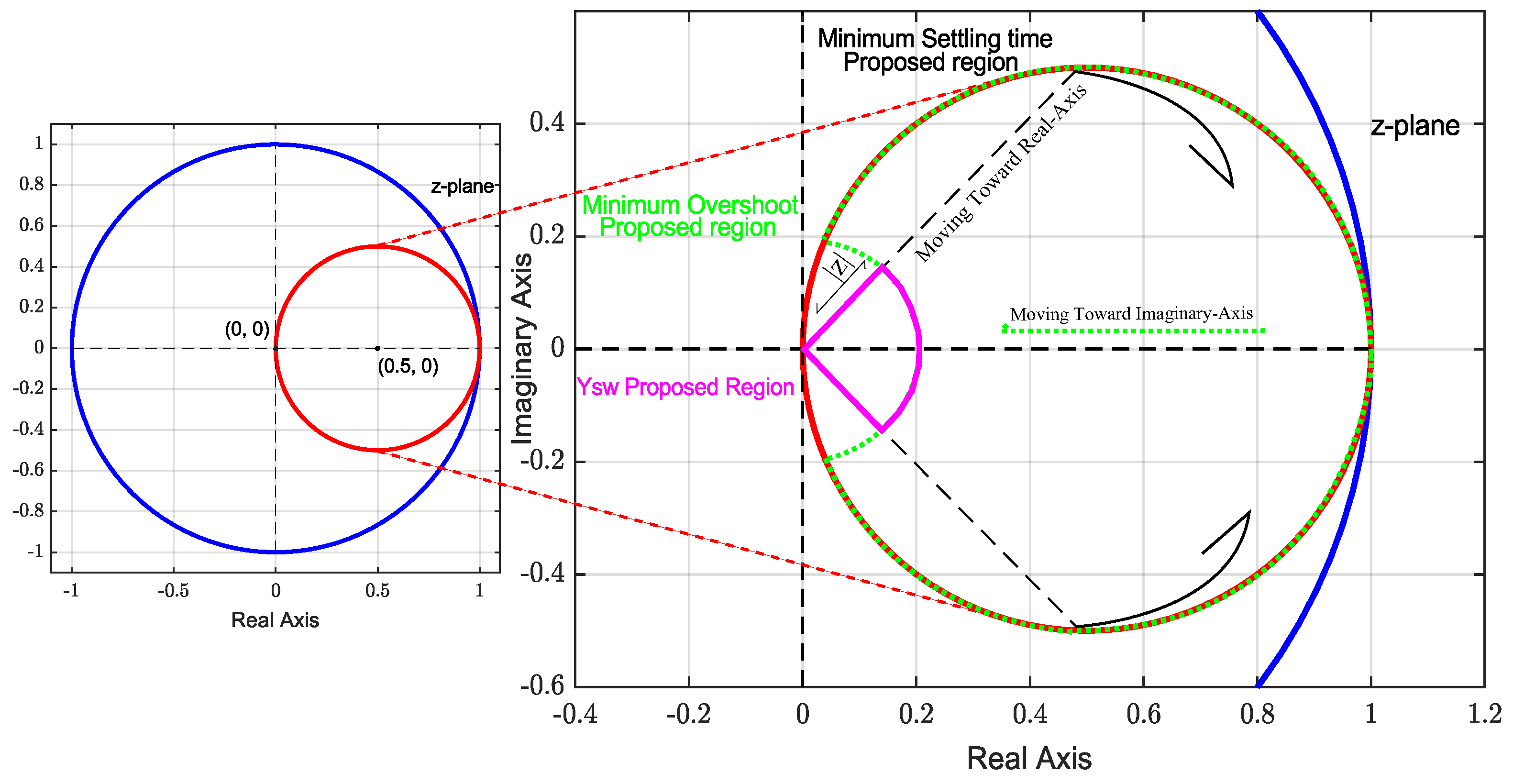
Figure 3 depicts the regions in which the system exhibits a rapid settling time and low overshoot, as indicated by Equations (
17) and (
18). The following is a representation of the regions situated within the complex plane. The shaded area represents one region of interest derived from the intersection of these two entities. As multiple minimum-overshoot and minimum-settling-time regions do exist inside the circle, multiple
proposed regions can be highlighted. Hence, the ADC model guarantees the absence of excessive overshoot or incorrect settling time by evaluating the discrete-state matrix’s eigenvalues (or dominating poles) and their appropriate placement within the designated region [
13].
4. ADC Switch Model Optimum-Parameters-Value-Selection Algorithms
The methodology employed in this research focused on determining and calculating the value of the ADC switch conductance by locating the system’s eigenvalues within a designated region in the z-plane. The primary aim was to reduce the negative effects of overshoot and settling time. The poles of the system were determined through the utilisation of the artificial bee colony (ABC), the firefly (FFA), and the genetic (GA) algorithms. The main rationale behind using nature-inspired optimisation methods and comparing their effectiveness (computation time and convergence rate) was their global exploration, which meant that the algorithms were able to search through a wide range of solution spaces. They were robust while dealing with complex systems and held a certain degree of easiness during implementation. No other algorithms were considered, which opens up the discussion to developing other optimisation methods in the future.
4.1. Artificial Bee Colony (ABC)
The ABC parameters consist of several factors, with the initial population size being the primary consideration. The user determines this value, which serves as a reflection of the optimisation problem’s complex nature. A larger initial population size has the potential to enhance the search process inside the designated search space. However, it is essential to note that an increased computing load may accompany this advantage. A limited initial population may restrict the range of search-space exploration yet facilitate faster convergence. The number of iterations for the second parameter is dependent upon the difficulty of the task. The selection of a significant number of iterations in the algorithmic process may facilitate the identification of the optimal solution. However, this approach may also increase the overall time necessary to complete the optimisation process. A low number of iterations could decrease the algorithm’s ability to sufficiently navigate the search space, hence decreasing the accuracy in identifying the ideal answer. It is customary to decide on an iteration number within a range from 100 to 1000, thereafter adjusting it in response to performance evaluations and the availability of computational resources [
14].
4.2. Firefly Algorithm (FFA)
The firefly algorithm (FFA) is an optimisation technique that draws inspiration from nature and emulates the flashing activity seen by fireflies to attract other fireflies. Fireflies employ bio-luminescence as a means of drawing in potential mates or prey, hence generating intricate patterns of luminous flashes inside low-light environments.
The firefly algorithm employs fireflies as a representation for the solutions, and the appearance degree of the solution is based upon its fitness value. Fireflies tend to be drawn towards other fireflies, influenced by the brightness emitted by the latter, which is closely linked to their overall fitness. More optimal solutions exhibit a greater degree of attraction among other fireflies.
The fundamental procedures of the firefly algorithm start with the creation of an initial population of fireflies, which will serve as the set of potential solutions. The fitness function is a mathematical representation used to assess the quality or effectiveness of solutions within the search space. The attraction of each firefly (solution) is determined by evaluating its brightness (fitness) in relation to other fireflies. The fireflies are directed towards more luminous fireflies inside the search region, with their positions being modified according to their attraction and the distance between them. The current light-intensity (fitness) status is being provided as an update. The fireflies’ light intensity (fitness) is modified per their updated spatial coordinates.
A well-constructed fitness function, also called the cost function, that accurately quantifies the performance of the problem in hand will ensure the solution quality by encapsulating the desired optimisation goals and mapping the fitness to the brightness. At the same time, the algorithm stores the optimal solution and compares it to the previous iteration’s best fitness solution. Ultimately, the optimal solution with the best fitness—in other words, the best metaphorical brightness—is outputted.
The process of attraction, movement, and intensity update should be iteratively repeated for a certain number of iterations or until a convergence requirement is satisfied. The utilisation of firefly migration towards brighter fireflies inside this algorithm facilitates efficient solution-space exploration. Customizing the algorithm’s attraction function and movement strategy is contingent upon the problem being addressed [
14].
4.3. Genetic Algorithm (GA)
The genetic algorithm (GA) is a widely utilised evolutionary computation methodology that draws inspiration from natural selection and genetics mechanisms. This algorithm is employed for the purpose of optimising and solving search-related problems.
An initial population comprised of potential solutions, sometimes referred to as individuals, is created. Typically, these solutions are encoded as binary strings; however, alternative representations may be employed, based on the nature of the problem, such as real numbers or permutations. The fitness function serves to measure the quality of a solution in relation to the specific problem being addressed. Solutions characterised by higher fitness values are indicative of superior performance in individuals.
The algorithm involves selecting existing population members as progenitors for future generations. Fitness levels often determine selection, with fitter population members being chosen. Selected parent pairs undergo a crossover process to produce children. Then, the algorithm mutates a portion of the offspring. Natural mutations cause tiny and random changes in the progeny’s genetic material. Genetic diversity is preserved in populations, to avoid early convergence to suboptimal solutions. Mixing the starting population, parents, and children creates a new generational cohort, as they replace less-fit individuals.
The GA algorithm is an effective approach to finding the optimal solution through selection, crossover, mutation, and replacement. The selection is linked to the number of generations, which is also linked to the number of iterations. Crossover and mutation are expressed in the algorithm as a probability. High crossover probability will increase the exploration by creating more diverse offspring, while low crossover probability will push for exploration with more maintained genetic information from the parent. The mutation probability indicates the likelihood of an individual’s chromosome going through mutation. High mutation probability will increase the exploration by adding random genetic changes, while low probability will set the algorithm exploration to be reliant on crossover. The typical values for crossover probability are between 0.6 and 0.9, and mutation probability is between 0.01 and 0.1. In our cases, the selection of 0.8 and 0.01 for the crossover and the mutation probabilities led to achieving the optimal answer.
The process of selection, crossover, mutation, and replacement should be iteratively performed for a certain number of generations or until a predetermined termination criterion is satisfied, such as reaching a suitable solution [
15].
For all the used algorithms implemented, by trial and error, increasing the initial population to more than 400 will not give different optimal results. It will increase the computation time. Decreasing the initial population to less than 400 will not give the optimal answer. This selected initial population did not lead to premature convergence, did not affect the algorithm’s robustness, and did not limit the search space. This stands for the selected test cases in this study.
4.4. Algorithms Cost Function
The cost function for the three algorithms (ABC, FFA, GA) is designed to minimise both overshoot and settling time. It is formulated based on the analysis done to the eigenvalue, as in
Section 3. The cost function is validated with the performance of real-world power converters as implemented in [
10,
13]. The initial element of the cost function, as outlined in Equation (
19), seeks to surpass the overshoot by minimising the total number of the squared eigenvalue angles:
Similarly, the second element of the cost function, derived from Equation (
20), can be expressed as the sum of the squared magnitudes of the eigenvalues. In both instances,
K represents the number of iterations. Multiplying each component of the cost function, denoted as
and
, by itself decreases the sensitivity of the eigenvalues that are in close proximity to the origin:
5. Case Studies
The typologies under investigation were full-bridge inverter, which is the basic building block for multiple-level inverters, like the three-phase nine-level CHB inverter; in this context, we examined one cell of the inverter. The second test case was the buck converter, to prove the diversity for the selection method for different types of switching devices. The associated-discrete-circuit-(ADC) method was employed, in order to construct a model for each of the cases.
The ADC approach employs an inductor and a capacitor to symbolize each switch during its activation and deactivation phases, as stated by source [
16]. The discrete formulation of an electrical switch is obtained by expressing it as a composite system consisting of a current source operating in parallel with a conductance. One significant advantage of this methodology is that irrespective of the switch’s state the conductance may be fixed by appropriately choosing a suitable time interval. Therefore, the circuit configuration may remain unchanged [
9,
11]. Additionally, the utilisation of the backward Euler (BE) integration method, renowned for its inherent damping characteristics, will lead to the discretisation of the elements inside the converter circuit and the derivation of the circuit’s matrix. The determination of nodal voltages and branch currents is an obvious outcome of resolving the discrete circuit matrix.
Three optimisation algorithms were proposed, in order to determine the optimal parameter values for the full-bridge and buck-converter models, which were implemented using ADC. The purpose of these algorithms was to address the limitations and disadvantages associated with the use of ADC. The primary advantage of utilising an algorithm for optimising ADC settings is its ability to tackle difficult and discrete optimisation problems efficiently. The utilisation of the above approach facilitated the practical examination of a broad spectrum of potential solutions, leading to faster convergence towards the ideal parameters [
17].
By employing network modelling techniques, like modified nodal analysis (MNA), it was possible to represent any conversion circuit equations in the form illustrated in Equation (
21). In this format, the switch admittance and its inverse were computed in advance, and the values of current and voltage were determined at each time interval
by solving Equation (
21). The matrix
was subject to change based on the switch state:
The computation of the circuit parameters occurred through a two-step process. The initial step was the computation of , whereas the subsequent phase relied on the history of the current sources. The process of updating was reliant upon the prior values of the voltages and currents. The utilisation of the network modelling technique allowed for the construction and simulation of the full-bridge circuit and buck converter, incorporating an ADC-based switch model.
Figure 4 shows the process of designing a power converter with the optimal parameter values of an ADC-switch-based model.
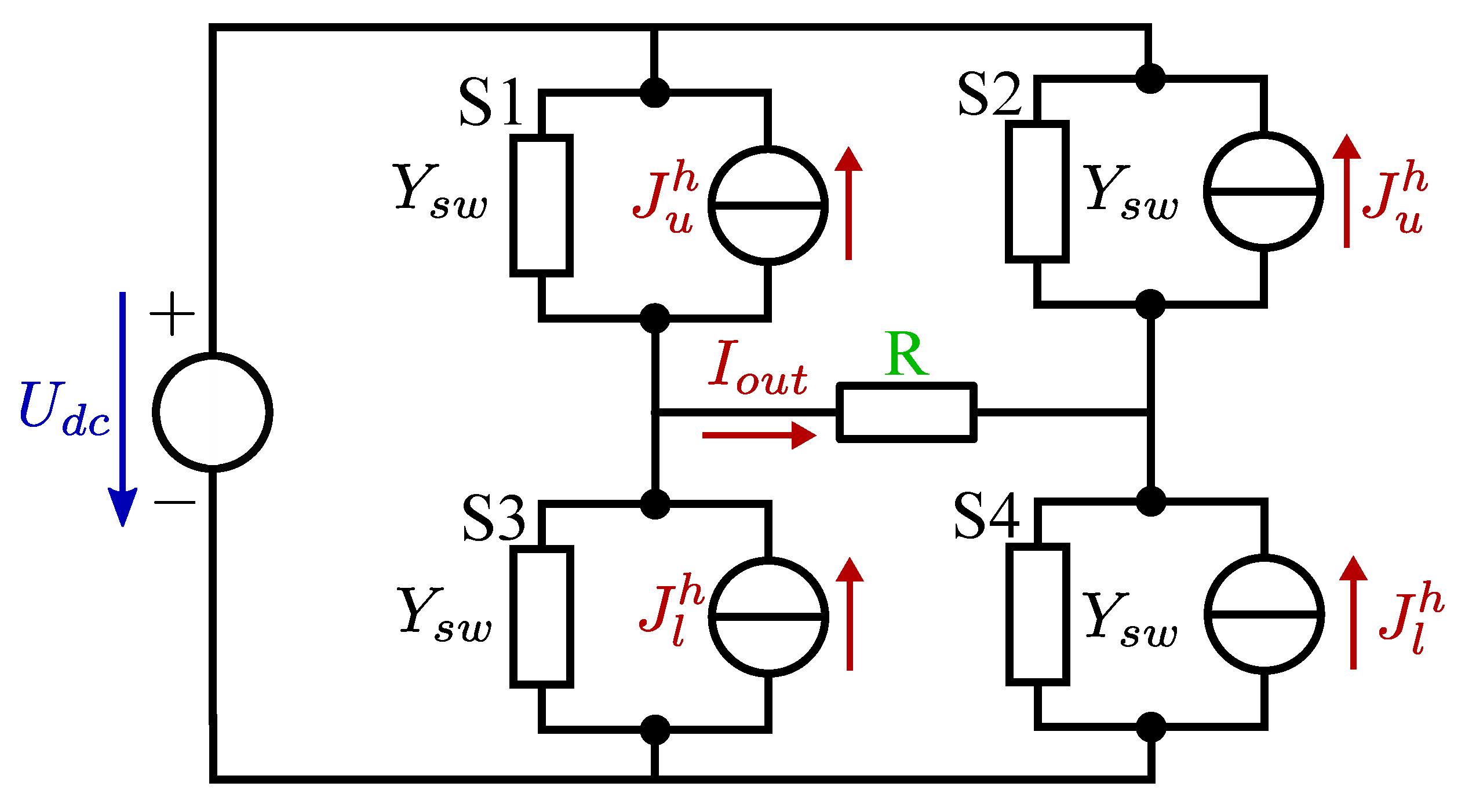
5.1. Full-Bridge Inverter
A block diagram of a full-bridge circuit with a resistive load is seen in
Figure 5. Matlab Simulink allowed us to conduct a simulation of the circuit, wherein the switch conductance was set to a value of 1. The switching frequency utilised in this study was 2 kHz. The modulation signal employed was a sine signal characterised by an amplitude of 0.95 and a frequency of 100
. This signal was compared to a triangle signal with a frequency of 2 kHz, to generate the gate signals. Additionally, the parameters used in the present study included a resistance value of 10 ohms (R), an input voltage of 100 volts (E), and a time interval of 200 nanoseconds (
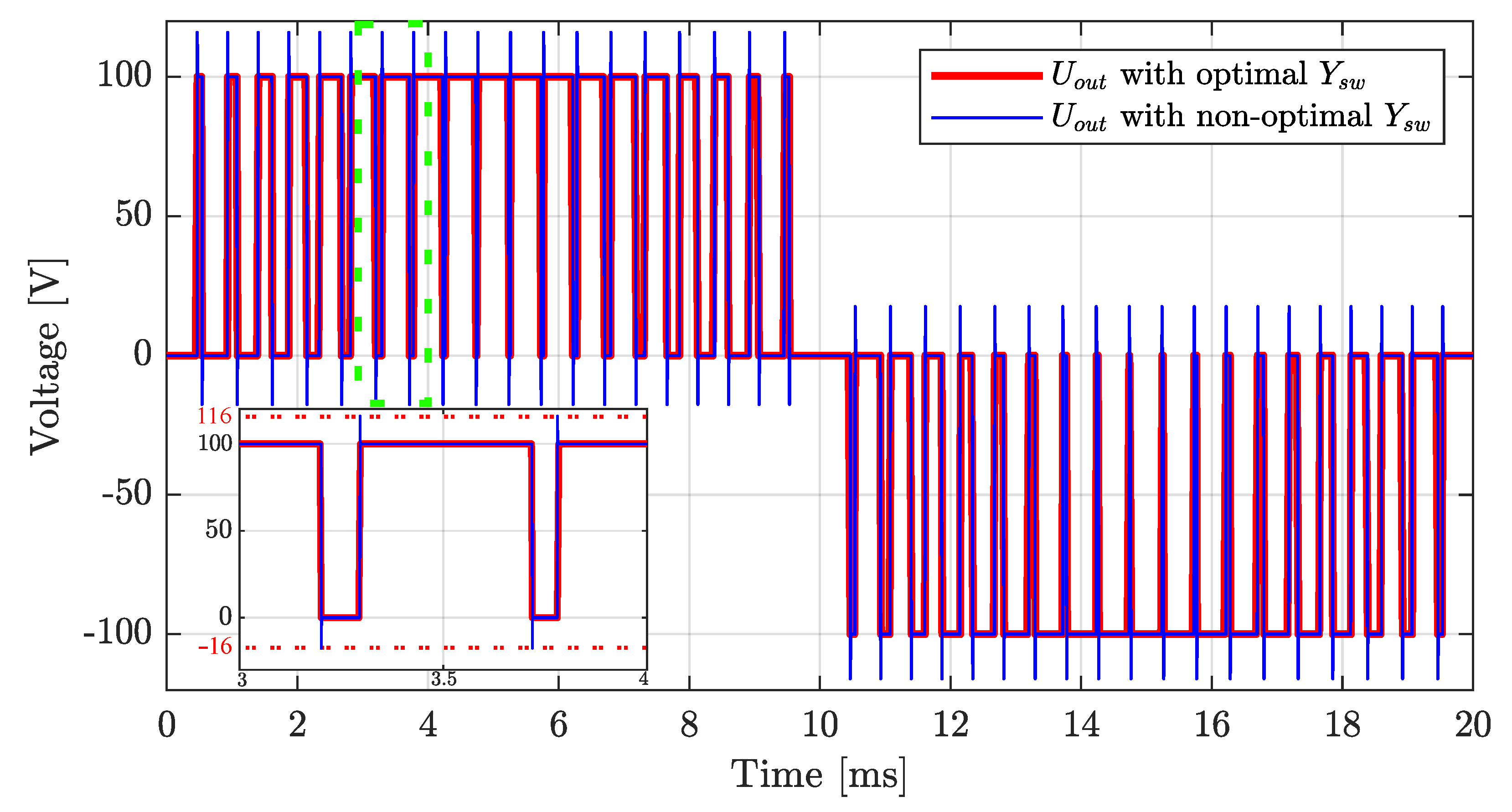
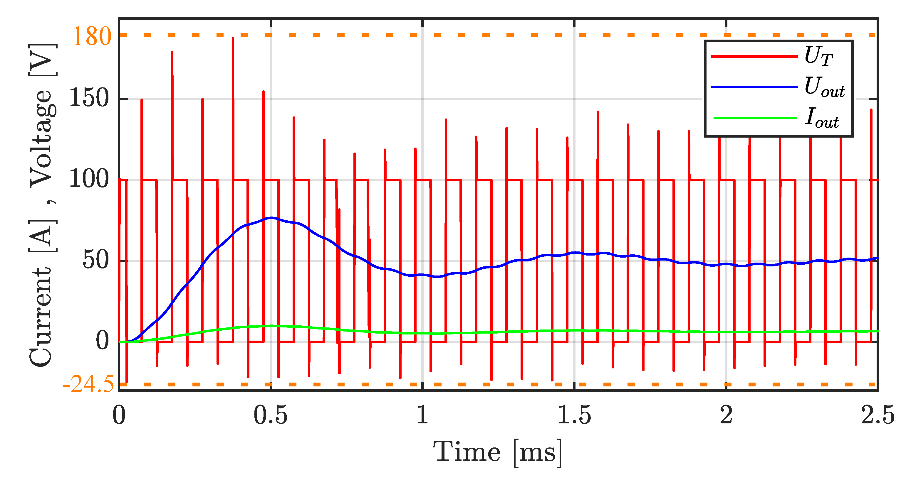
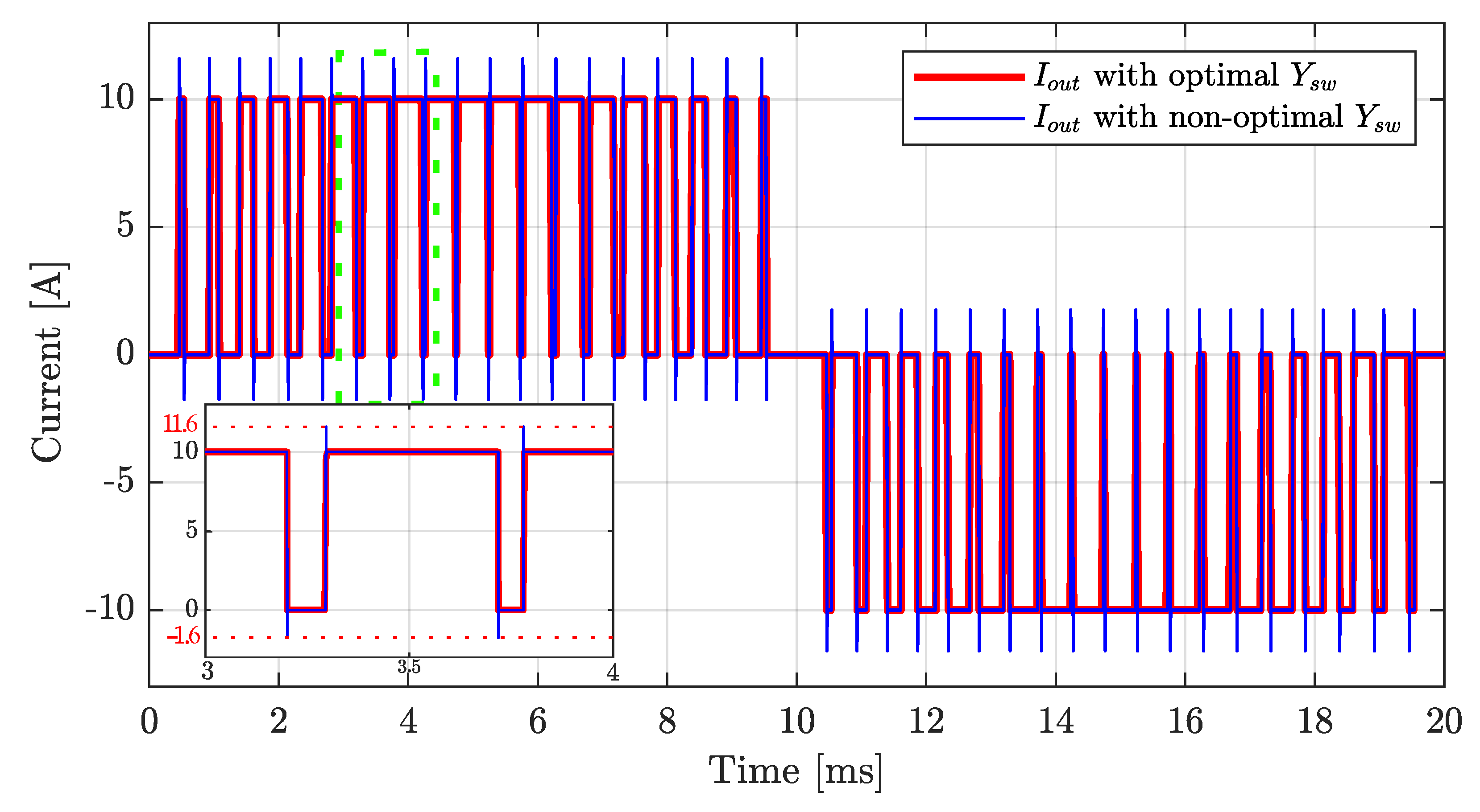
). The effect of the resistance value on the output result was recorded, but no further sensitivity analysis was conducted, while the selected value, R = 10 ohms, ensured a minimum effect in our test case. The simulation results are depicted in
Figure 6 and
Figure 7. The occurrence of transient spikes in both the output voltage and current was noted, resulting in notable virtual power losses inside the ADC model.
The full-bridge circuit can be simplified into two distinct topologies. The first topology occurred when switches 1 and 4 were closed, whereas the second topology occurred when switches 2 and 3 were closed. The state-space matrix of the circuit was constructed and subsequently discretised using the backward-Euler-integration approach. Additional details regarding the derivation and discretisation procedure can be found in the publication referenced as [
13]. Equation (
22) displays the state-space matrix of the full bridge:
The discrete-state-space matrix could be obtained based on the variable
as stated by backward Euler, as in Equation (
23). According to the eigenvalues of Equation (
23), the ABC, GA, and FFA algorithms were employed to find the optimal values of
:
Table 1 shows the optimized values for
, for which the eigenvalues of the
matrix are located in the marked area as described in
Section 3. Within the boundaries of
, an optimum answer for
was found for each run of all the algorithms, resulting in an adequate outcome.
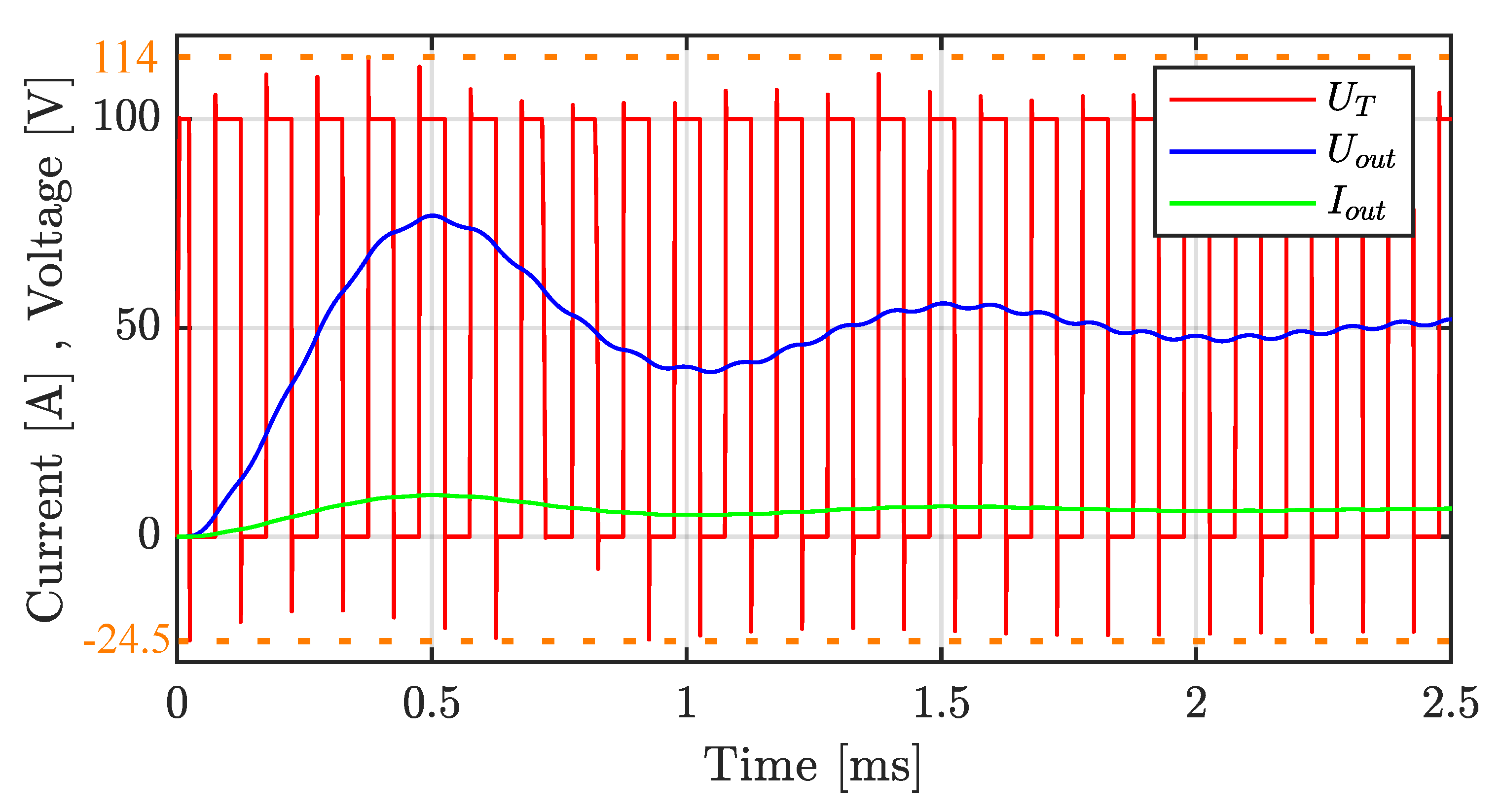
Table 2 gives a performance comparison between the algorithms, while locating the conductance optimal value for the full-bridge inverter. Even when changing the number of iterations, as this was one of the primary factors that influenced the computational speed and the convergence rate, it can be seen that the FFA had the lowest convergence rate—hence, the highest computation time. By contrast, the GA algorithm achieved the most down computation time and the highest convergence rate. ABC stood in the middle with both values. Changing the number of iterations did not change the optimal value achieved, it was observed to be between 0.09966 to 0.10098, with no effect on the output voltage and current.
Figure 8 show the presence of two light-blue poles on the z-plane within the positive and negative Imaginary axis with non-optimal settings resulting in an overshoot. On the other hand, the green poles located on the Real axis were associated with ideal parameters. The specified region within the complex plane might be considered an approximate area. Therefore, not all poles were expected to be situated in a precise and specific location.
5.2. Buck Converter
As shown in
Figure 9, a buck converter was modelled using ADC, a switch (
), and a diode (
), with no dead time. We can use Equation (
24) to represent the buck converter state-space matrix, capturing the switches in the ON state and OFF state. In the steady-state analysis, there were two cases: the first case included the upper switch (
) to be turned on and the diode (
) turned off; in the second case, the upper switch (
) to be turned off and the diode (
) to be forward biased, which signified, in ADC modelling terms, that the model would change from capacitor to inductor, to indicate that the diode was in the ON state and, as stated previously, a virtual power loss would take place. The state-space matrix of the buck converter is shown in the following equations, where the discrete-state-space matrix can be obtained based on the variable
, as stated by backward Euler, as in Equation (
25).
Figure 10 shows the circuit’s output voltage and current, with non-optimal conductance value.
Table 3 shows the optimized obtained values of parameter
for the ADC-switch-based model of the buck converter using the ABC, FFA, and GA algorithms.
Figure 11 shows the circuit’s output voltage and current, with the optimal values achieved by all three algorithms.
Table 4 gives a performance comparison of the algorithms while locating the conductance optimal value for the buck converter. Once again, the ABC is set in the middle, regarding the computational-time and convergence-rate values, while the FFA was the slowest to complete the process to locate the optimized value, and the GA was the fastest to converge to the optimal value. The case remained the same, even when changing the number of iterations.
The values for percentage overshoot (PO) and settling time are provided in
Table 5. When both systems were configured with optimum values (
= 0.1) for the full-bridge inverter and (
= 0.5) for the buck converter, the full-bridge circuit exhibited reduced overshoot and settling time for both the output voltage and current compared to the arbitrarily chosen non-optimal parameters. The outcome obtained through the utilisation of these optimal values bears a resemblance to an inverter circuit with ideal switch behaviour. The buck-converter circuit exhibited significantly reduced overshoot and settling time of the transistor voltage, with a percentage overshoot reduction of around 64% and settling time decreased from 1.5
s to 0.5
s, which brought the buck converter to more realistic behaviour.
More test cases need to be conducted to confidently generalize this method. Although, based on the literature and the result in this paper, we can apply the method to not only power converters but also to transmission lines [
10]. The limitation to this method is the complexity of the system, as it will be harder to obtain the system’s state-space matrix with ADC implementation and to move forward with the optimisation.


