Article

Design and Implementation of a Paralleled Discrete SiC MOSFET Half-Bridge Circuit with an Improved Symmetric Layout and Unique Laminated Busbar

1
Aselsan Inc., Yenimahalle, 06200 Ankara, Türkiye
2
Department of Electrical Engineering, Istanbul Technical University, Maslak, 34469 Istanbul, Türkiye
*
Author to whom correspondence should be addressed.
Energies 2023, 16(6), 2903; https://doi.org/10.3390/en16062903
Submission received: 22 February 2023 / Revised: 15 March 2023 / Accepted: 19 March 2023 / Published: 21 March 2023
(This article belongs to the Special Issue Advances in Design and Control of Power Electronic Systems)

Abstract

:
Silicon carbide (SiC) metal oxide semiconductor field effect transistors (MOSFETs) have many advantages compared to silicon (Si) MOSFETs: low drain-source resistance, high thermal conductivity, low leakage current, and high switching frequency. As a result, Si MOSFETs are replaced with SiC MOSFETs in many industrial applications. However, there are still not as many SiC modules to customize for each application. To meet the high-power requirement for custom applications, paralleling discrete SiC MOSFETs is an essential solution. However, it comes with many technical challenges; inequality in current sharing, different switching losses, different transient characteristics, and so forth. In this paper, the detailed MATLAB®/Simulink® Simpscape model of the SiC MOSFET from the datasheet and the simulation of the half-bridge circuit are investigated. Furthermore, this paper proposes the implementation of the four-paralleled SiC MOSFET half-bridge circuit with an improved symmetric gate driver layout. Moreover, a unique laminated busbar connected directly to the printed circuit board (PCB) is proposed to increase current and thermal capacity and decrease parasitic effects. Finally, the experimental and simulation results are presented using a 650 V SiC MOSFET (CREE) double-pulse test (DPT) circuit. The voltage overshoot problems and applied solutions are also presented.

1. Introduction

Wide bandgap semiconductor technology is a very popular and growing technology for numerous industrial applications that require a high power density [1]. SiC-based semiconductors are especially very common with low drain-source resistance, high thermal conductivity, high blocking voltage, and high switching frequency compared to the old semiconductor technology (Si-based) [2]. However, it is challenging to replace Si-based power components with SiC ones for every customized application due to the unavailability of a wide range of high-power SiC modules. Paralleling discrete SiC MOSFETs is the critical solution to increasing the power and current capability of customized systems.
MOSFET paralleling seems like a straightforward process. Additionally, the positive temperature characteristic of the on-state resistance of the MOSFET helps to balance the steady-state current of the device. However, it is challenging, especially for high current ratings. Fabrication mismatches ( R d s ( o n ) , V t h , etc.), parasitic effects, layout differences, and so forth must be handled to balance the currents of the paralleled MOSFETs, particularly in the transient region. Fabrication mismatches of MOSFETs directly affect the switching action, and any distortion of symmetry of the circuit layout results in different parasitic effects. These differences cause an imbalance in the current sharing of the paralleled MOSFETs, resulting in different losses and thermal imbalances. In addition, the system must be thermally balanced to protect current sharing and system performance. At that point, the increased current capacity provided by paralleling makes thermal problems difficult to solve on the PCB. A laminated busbar can be used to prevent the PCB from carrying a high current, which behaves as a heat sink and releases heat. Although the laminated busbar decreases the inductance of the current path, which reduces the voltage overshoot caused by the switching action, an increase in the switching speed of the SiC MOSFETs can also cause voltage overshoot problems.
Studies have been performed on the current sharing of paralleled MOSFETs, which can be categorized into two groups, passive and active current balancing. In general, active current-balancing methods require high-bandwidth sensors and complex current-balancing circuits. Besides that, passive current balancing methods increase the size of the circuit by adding inductors, capacitors, and chokes acting as passive circuit elements. In Ref. [3], the current imbalance of two paralleled SiC MOSFETs in the transient switching region was compensated with an active current balancing method. In this method, the difference in unbalanced currents is sensed with a differential current transformer. Sensed unbalance is eliminated by the active gate control circuit. According to its results, this method works fine in the transient region; however, the current balance is more distorted in the steady-state region. Furthermore, paralleling more than two MOSFETs with this method seems more complicated. Instead of using a differential current transformer to measure the difference of the magnitude of unbalance in currents, a planar Rogowski coil-based current sensor was proposed in Ref. [4]. However, using a current sensor circuit increases the complexity of the system. Moreover, in Ref. [5], the current sharing of paralleled SiC MOSFET modules is balanced with the active gate driver circuit. The edge and slopes of the drain currents are detected with the help of a voltage of source inductance. The gate driver voltage is dynamically adjusted according to the drain currents. This method provides balanced current sharing between SiC modules after a few switching cycles. However, dynamic control of the gate driver voltage increases the complexity of the circuit. In addition, a detailed analysis is required to detect the edges and slopes of the drain current of the parallel units. A passive transient current balancing circuit is used for three parallel SiC half-bridge units in Ref. [6]. This circuit provides a current balance, but it increases the size of the circuit by adding an inductor to the power line. Additionally, the effectiveness of that current-balancing circuit in paralleling a discrete SiC MOSFET should be further analyzed because it was found in Ref. [7] that the parallel half-bridge unit has a smaller current imbalance compared to the paralleling of the die. In another study, Ref. [8], peak currents of paralleled SiC MOSFETs were balanced with the help of drive-source resistance and coupled power inductors. However, detailed analysis is required to select the effective values of the passive elements. Additionally, these elements increase the size of the circuit. On the other hand, the current balance of the paralleled SiC MOSFETs was provided using only the differential mode choke in Ref. [9]. This method is successful for current balancing in both transient and steady-state regions. However, adding a differential mode choke to the power line increases the circuit size, and paralleling more than two MOSFETs increases the difficulty of the mechanical implementation of chokes. Furthermore, a detailed analysis is required to determine the properties of the differential-mode choke.
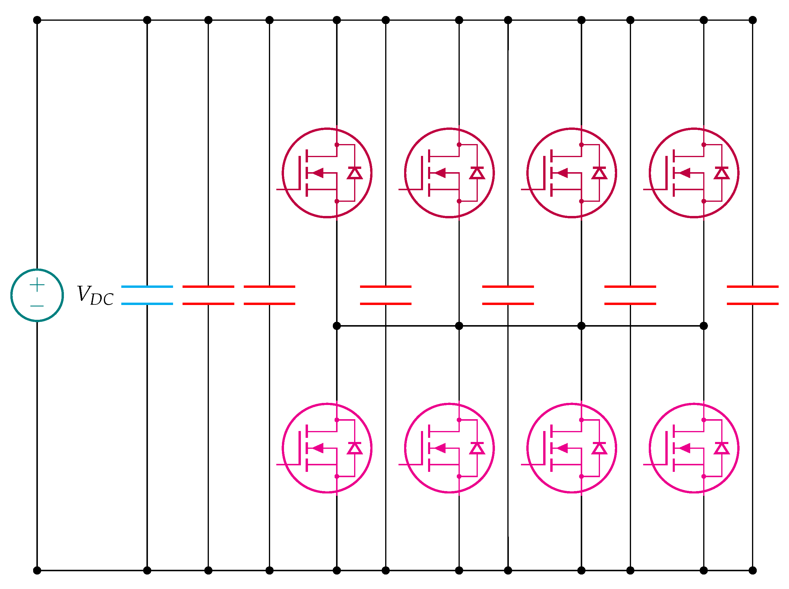
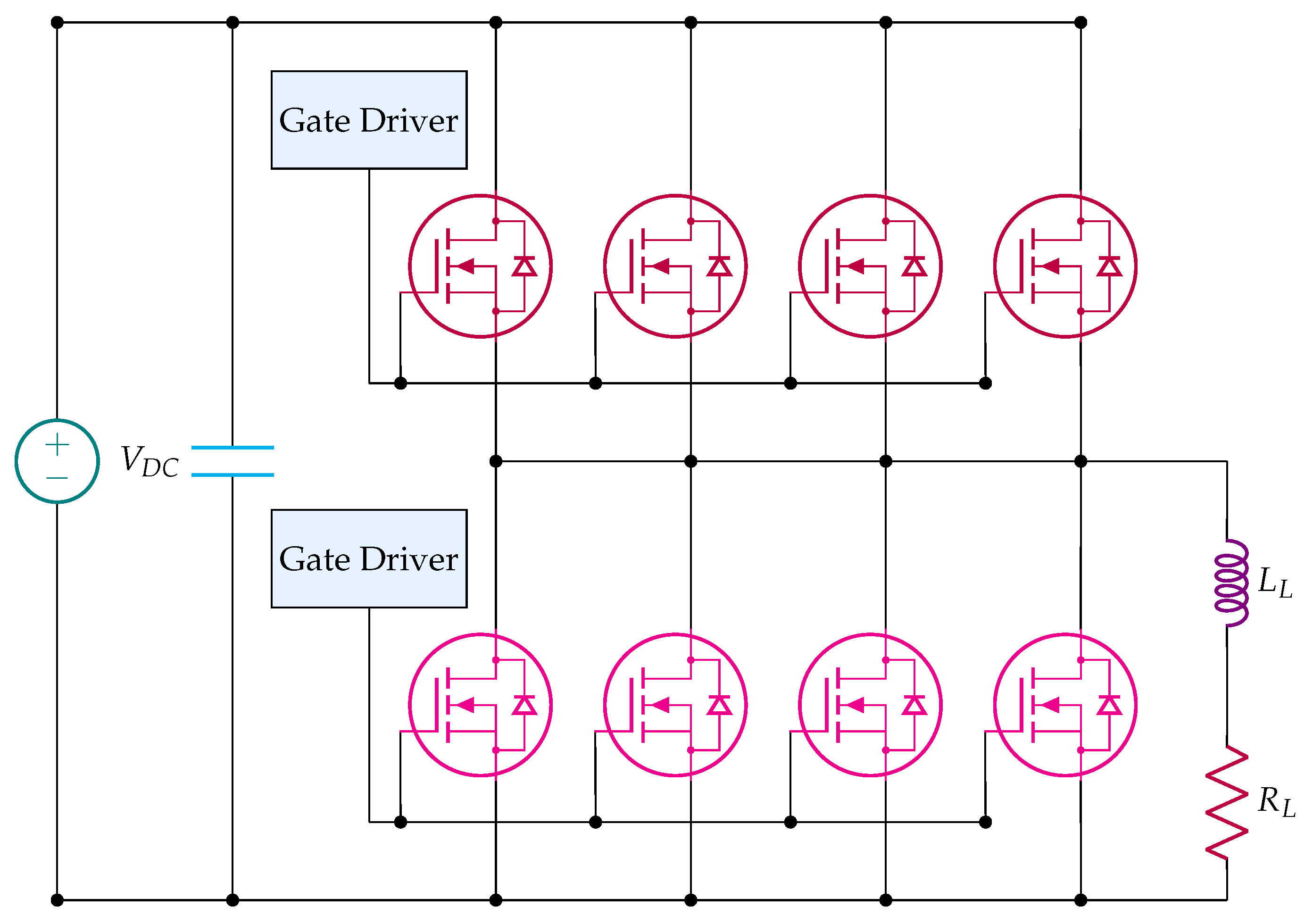
The main purpose of this work is to construct a switching leg composed of paralleled SiC MOSFETs that does not include any passive or active current balancing circuit without any current imbalance. The proposed half-bridge circuit schematic composed of four paralleled SiC MOSFETs is shown in Figure 1. One gate driver circuit is used for the four parallel connected SiC MOSFETs. For the half-bridge circuit topology, two gate driver circuits are used, one for the high side and one for the low side of the leg. DC source and DC-Link capacitance are connected to the DC side of the circuit. R and L are the passive loads for the circuit. All of the connections are provided on the PCB, except DC and phase connections. These connections are provided with the help of a laminated busbar.
This paper is composed of five sections. In Section 2, the simulation model of the SiC MOSFET is explained. In Section 3, the hardware of the system is detailed. Experimental results are shown in Section 4. Finally, Section 5 summarizes the critical points of this paper.

2. Simulation Model of SiC MOSFET

Modeling of switching instants for any switching device is difficult for the simulation environment due to the nonlinearity of elements and the limitation of computation performance. In particular, modeling wide-bandgap semiconductors is more difficult due to the high switching speed, which causes a challenging trade-off between computation time and complexity of modeling. Mainly, the modeling of semiconductors can be categorized into two groups: analytical and behavioral models. At this point, behavioral models are more appropriate compared to analytical models because equations of physical modeling that include the nonlinearity of elements require excessive computation. In Ref. [10], the analytical model of SiC MOSFET in a DPT circuit is explained in detail; however, intensive equations are used. In the same way, a detailed analytical model of the SiC MOSFET for the bridge-leg configuration is constructed in Ref. [11]. However, it also requires a complicated equation. On the contrary, behavioral models use the I-V and the capacitance curves (C-V) of the device. Both of them can be obtained easily from the datasheet. Data sets can be extracted from datasheet graphs with the help of any curve-fitting tool [12]. In this research, the Plotdigitizer [13] program is used to accurately extract data sets from datasheet graphs.
Data sets are obtained from the datasheet of the Wolfspeed CREE-C3M0015065K SiC MOSFET [14], which is shown in Table 1, Table 2, Table 3 and Table 4. Table 2 and Table 3 show the MOSFET I d s current with respect to the V g s & V d s voltages. The datasheet provides first and third quadrant graphs of I d s & V d s for different V g s voltages. The first quadrant graph includes the range of 0 V–10 V for V d s and 7 V, 9 V, 11 V, 13 V, and 15 V values for V g s . Furthermore, the third quadrant graph includes the range of −8 V–0 V for V d s and values of 0 V, 5 V, 10 V, and 15 V for V g s . According to Table 2 and Table 3, missing parts of the datasets are calculated using a linear interpolation method. Although the I d s graph is non-linear, the linear interpolation method is a handy tool to obtain the approximated I d s graph for different V g s voltages. The reason is that approximated curves are close to each other, and they can be considered parallel. Moreover, it also makes the calculation process easier. Negative V g s values are added to the bottom of Table 2 and Table 3 with zero current value because this part is modeled under the body diode model. Table 1 shows the body diode I d s current with respect to the V g s & V d s voltages. The body diode current graph from the datasheet provides the range of −7 V–0 V for V d s and 0 V, −2 V, and −4 V for V g s . However, 0 V, −2 V values for V g s are not modeled due to the customization options of a simulation program. I d s current values for V d s = −10 V, −9 V, and −8 V are calculated with a linear interpolation method for the body diode. Table 4 shows the internal capacitance values with respect to V d s voltage. Internal capacitances are C i s s (input capacitance), C r s s (reverse transfer capacitance), and C o s s (output capacitance).
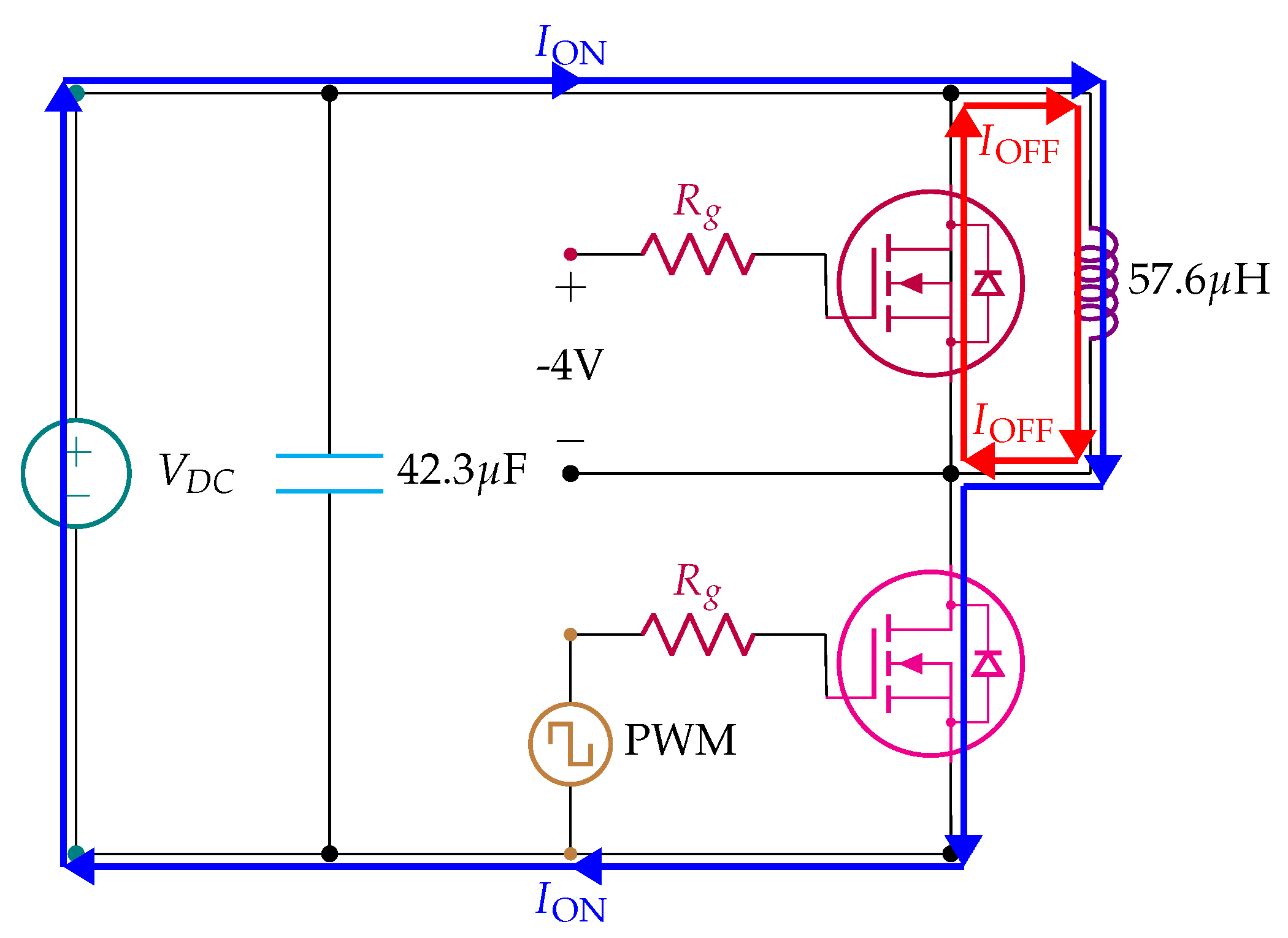
MOSFET and diode models of Simscape blocks of the MATLAB®/Simulink® have many options to customize the model. The obtained datasets are implemented in Simscape blocks using this property; therefore, most of the non-linear parts of the switching instant are modeled. Moreover, a reverse recovery model of the body diode is implemented with the “charge dynamics” option of the Simscape diode model. The peak reversed current, initial forward current, rate of change of current, and charge quantity properties from the datasheet are implemented in the model. However, the datasheet provides these properties only for the 175 °C junction temperature and 55.8 A initial current value. Therefore, only that condition is modeled for reverse recovery. In addition, sample time and solver type are essential factors for simulation time. The backward Euler solver is used with the 1 × 10 9 sample time, which many computers can handle. This sample time is obtained with a trial-and-error method according to the trade-off between the processing time and the resolution of the results. It is mainly affected by the switching frequency, which is 12.5 kHz. A double-pulse test (DPT) circuit is used to verify the MOSFET and diode models, shown in Figure 2. In the DPT circuit, a high-side MOSFET is switched off for the entire switching period. Its body diode is used as a free-wheeling diode for the parallel connected inductor, but low side MOSFET is switched with 15 V/−4 V PWM. The R g value is set to 5 Ω , and V D C is selected as 400 V. Values of passive elements and applied voltages are selected according to the DPT circuit of the MOSFET datasheet to compare the same cases. When the low-side switch is turned on, current flows through the inductor and low-side MOSFET. For that period, the current magnitude is increased according to the well-known formula given in Equation (1); therefore, the switching current value of the low-side MOSFET is adjusted by modifying the duty cycle. Besides that, the current on the inductor flows through the body diode of the high-side MOSFET when the low-side switch is turned off. In this way, the MOSFET’s turn-on and turn-off losses can be calculated.
d i L d t = V D C L
where V D C is the applied DC voltage, i L is the inductor current, and L is the inductance value.
Comparison of switching losses is a valuable indicator to verify the simulation model. Therefore, switching losses are calculated with the DPT circuit in the simulation program for the low-side MOSFET. The calculated values are compared with the datasheet values; the results are shown in Table 5. To compare the accuracy of results, total loss error (TLE) calculation is used, which is shown in Equation (2). As seen in Table 5, the maximum mismatch of the total error is less than 10% for all current ratings. The turn-on loss mismatch is the significant portion of the mismatch because the turn-off losses are closer to the datasheet values than the turn-on losses. When the low-side MOSFET is switched to turn-on, the current of the inductor and the reverse recovery current of the high-side MOSFET body diode are superposed. Therefore, the main reason behind the mismatch of the turn-on loss is caused by the reverse recovery model of the body diode. As explained above, only the 175 °C junction temperature and 55.8 A initial current value case of the diode can be implemented. However, the mismatch in the turn-on loss, less than 10% of the total loss mismatch, is in an acceptable range. Furthermore, the current and voltage curves of the MOSFET and diode are implemented in detail in the simulation model. For this reason, the conduction losses calculated in the simulation are the same as the conduction losses in the datasheet based on the value R d s .
T L E ( % ) = ( E o n + E o f f ) s i m u l a t i o n ( E o n + E o f f ) d a t a s h e e t × 100
where, TLE is the total loss error, E o n and E o f f are the turn-on and turn-off energies of the MOSFET, respectively.

Simulation of Half-Bridge Circuit with Four Paralleled SiC MOSFET

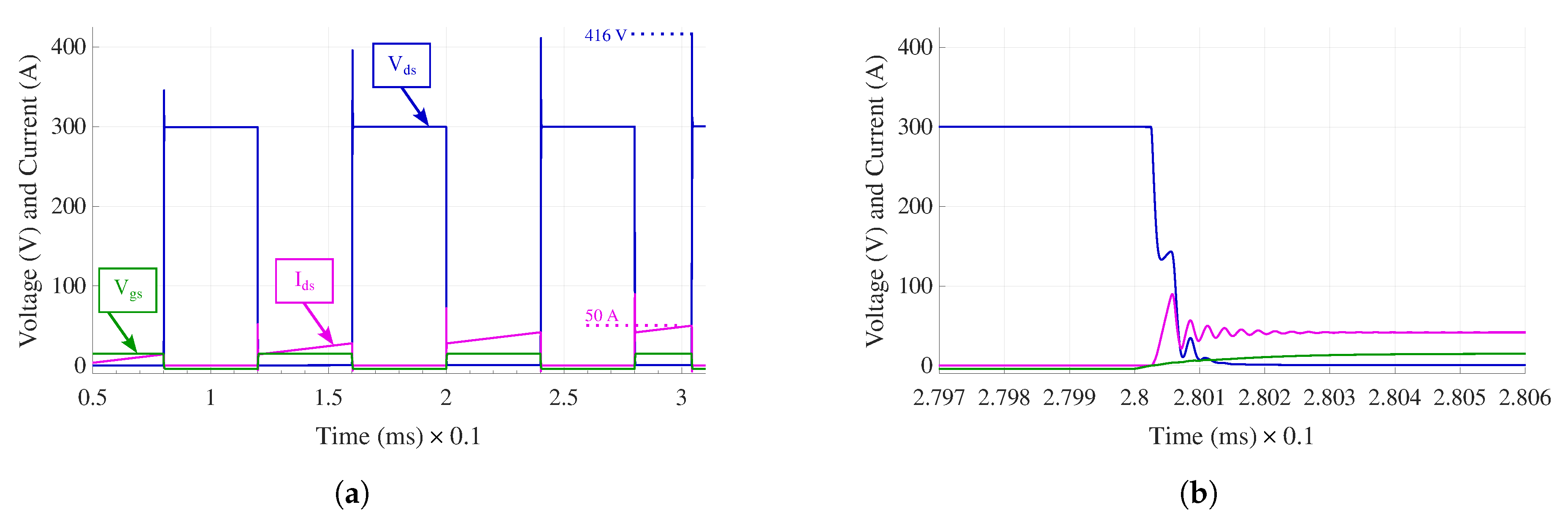
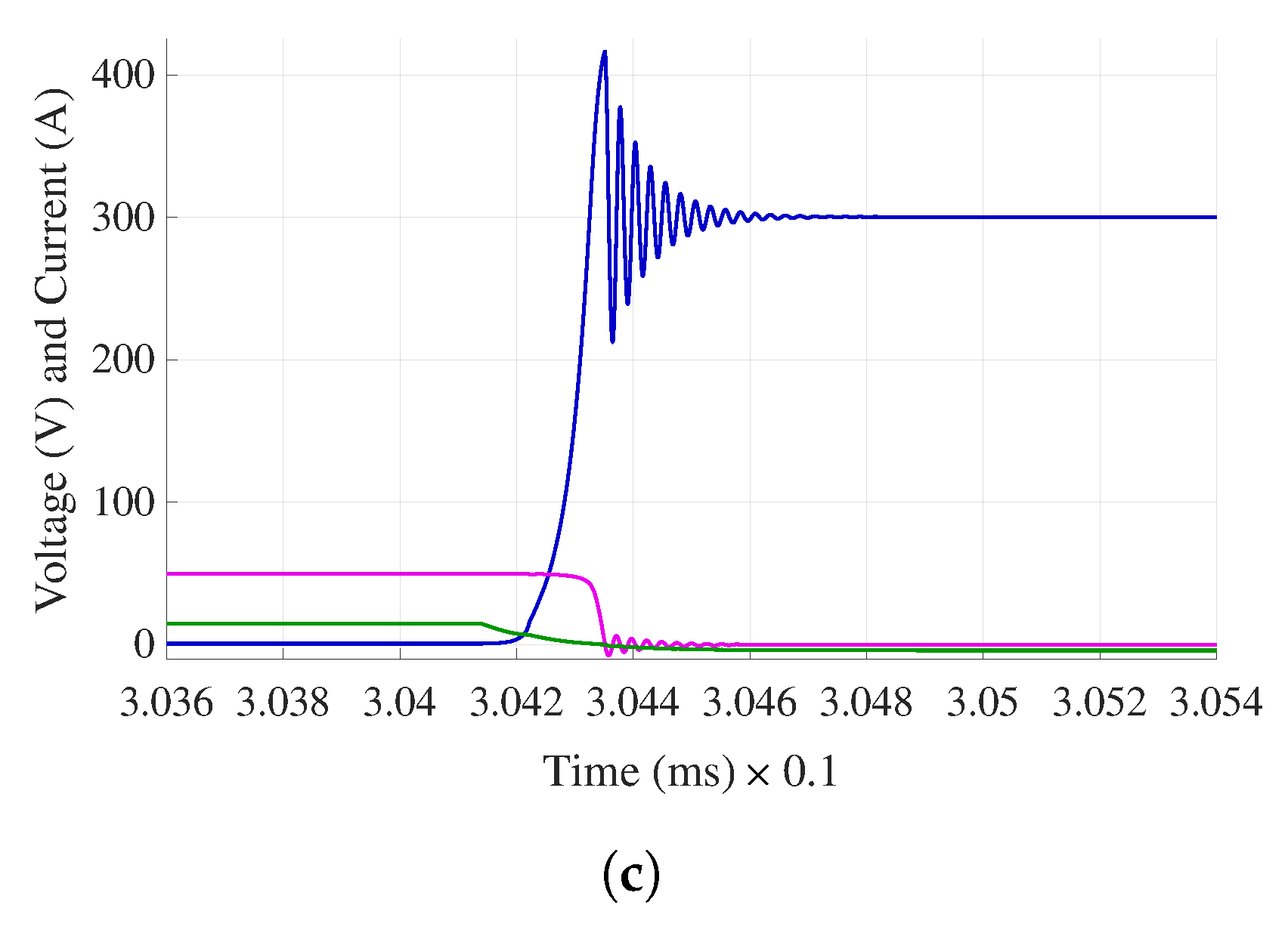
The half-bridge circuit with four paralleled SiC MOSFET, as shown in Figure 1, is run with the obtained model of the SiC MOSFET in the simulation program. The laminated busbar model is implemented into the simulation model by equivalent resistance, capacitance, and inductance values. These values are obtained by measurement with an LCR meter. The gate resistance of 10 Ω is used for the SiC MOSFETs, and the 220 μ H inductor is used as a load. Furthermore, 82 μ F capacitance is used for the DC-Link. In the simulation, equal current sharing is observed between parallel connected MOSFETs. However, voltage overshoot problems are observed in the V d s voltage when a turn-off case is applied. For the 50 A I d s current of MOSFETs, 416 V overshoot is observed for the 300 V switching voltage. That corresponds to 38% voltage overshoot. The applied switching waveform and the voltage overshoot are shown in Figure 3.
3. Hardware Design and Description

In this part, the design of the gate driver circuit and the layout of the power circuit are explained in detail. First, the calculation of the power of the gate driver circuit, the layout design, and the placement are given. Then, the high-voltage part of the half-bridge circuit is described.

3.1. Gate Driver Design

Using the same gate driver circuit for parallel MOSFETs has advantages compared to separated MOSFETs in terms of circuit size and the number of components. However, this comes with challenges in power requirements and gate driver layout during the circuit design process. In this study, one gate driver is used for four paralleled MOSFETs, one for the high side and one for the low side of the half-bridge. Separated turn-on gate resistors, turn-off resistors, and Miller protection paths are used to decrease interference between devices. Parallel devices increase the power requirements of the gate drive circuit. The gate driver circuit must be the source and sink of the peak gate current and average current. The average current can be calculated with Equation (3) [15]. To calculate the worst case, the switching frequency can be higher than the planned frequency. The gate charge value is taken from the datasheet.
I g a t e ( a v g ) = f × Q × n = 20 kHz × 188 nC × 4 = 15.04 mA
where, Q is the gate charge, f is the switching frequency, and n is the number of parallel devices.
The average gate current is small compared to the peak gate current. Because of that, the peak current must be checked. The peak gate current of the gate driver circuit is calculated using Equation (4) [16]. R g ( i n t ) of the MOSFET is 1.5 Ω , from the datasheet. The datasheet advises that R g is taken as 5 Ω .
I g a t e ( p e a k ) = ( V G ( o n ) V G ( o f f ) ) R g ( e x t ) + R g ( i n t ) × n = 15 V ( 4 V ) 5 Ω + 1.5 Ω × 4 = 11.69 A
where, R g ( e x t ) refers to the external gate resistance, R g ( i n t ) refers to the internal gate resistance of the device, V G ( o n ) and V G ( o f f ) refer to the turn-on and turn-off gate voltages of the device, respectively.
According to the calculations, a 10 A-rated gate driver integrated circuit is selected. This current rating is lower than the required peak current; however, capacitors are known to supply a large portion of the peak current. Furthermore, 70% of the peak current is enough according to Ref. [17] for a non-oscillated gate loop.
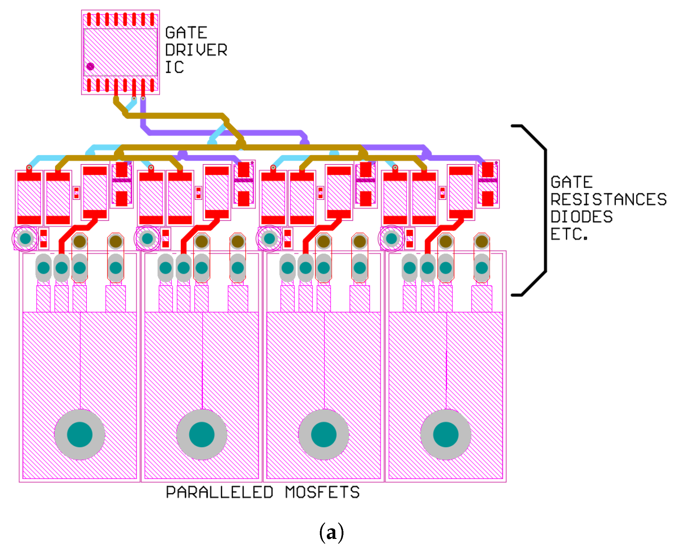
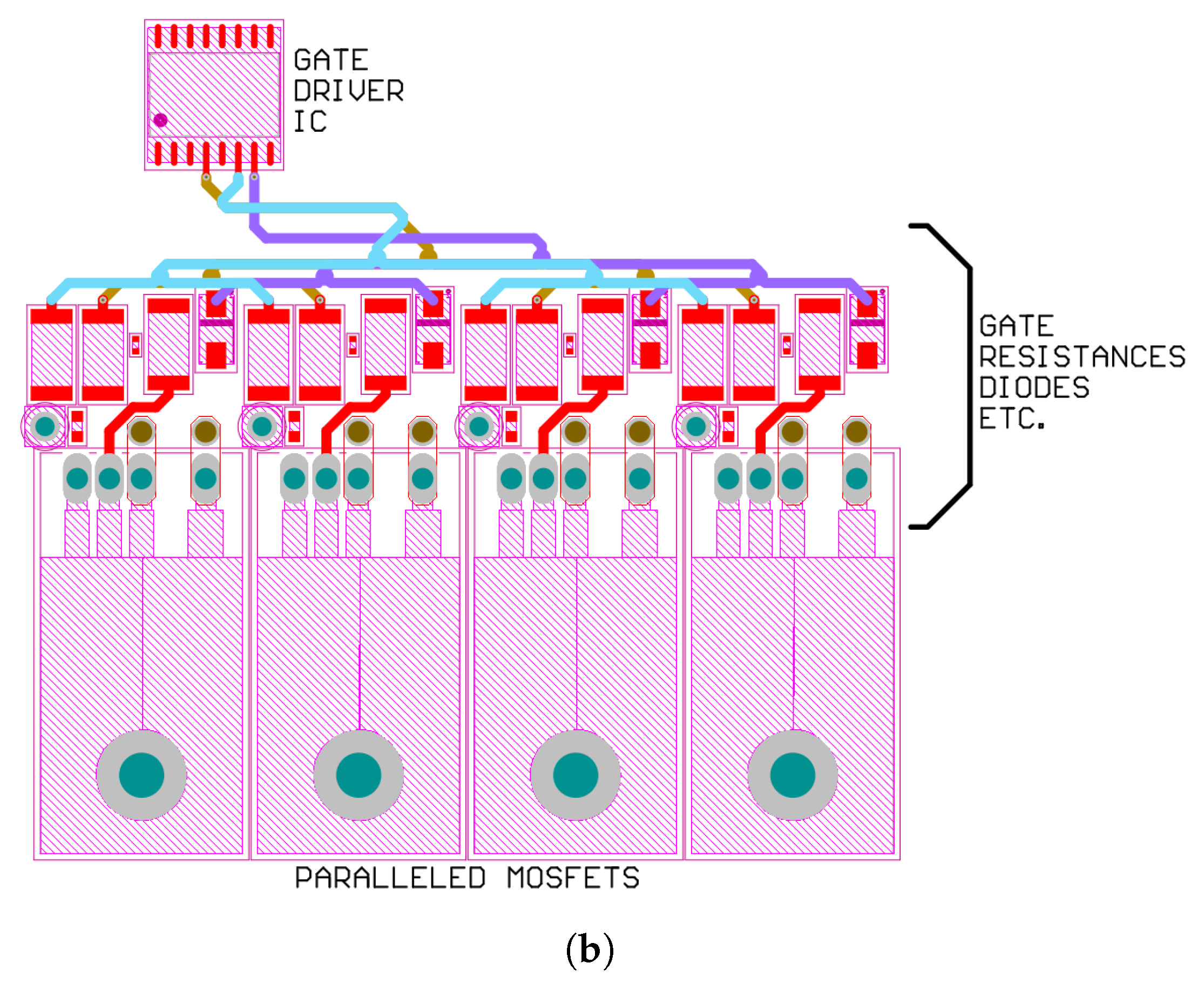
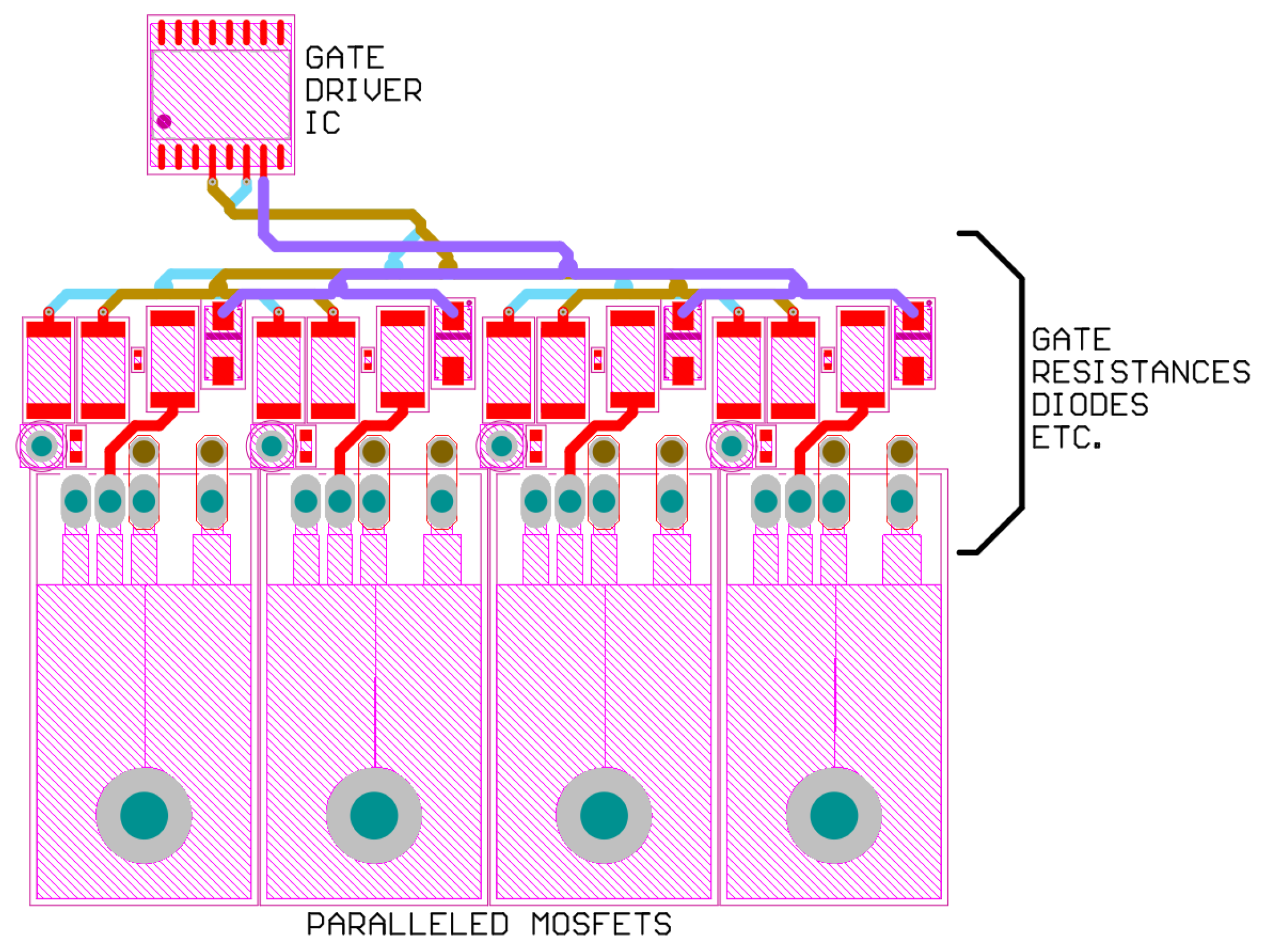
All parallel connected MOSFETs must reach the gate signal at the same instant. This is an important point for the equal current distribution between MOSFETs. The laminated busbar technique is used in Ref. [18] for the gate signal loop. However, it is not the preferred solution because it will cause an increase in parasitic capacitance. As a result, the switching speed slows down, and the switching losses increase [19]. Moreover, a slower switching speed increases the current mismatch between paralleled SiC MOSFETs [20] because the mismatch of the device parameters becomes more effective by increasing the switching time. Although the parasitic inductances of the gate signal paths in the devices are decreased, symmetry and equality of the gate signal path will be lost. As a result, the inequality in the propagation delay of the gate signal path causes asynchronous switching and current mismatch between parallel MOSFETs. To protect against a current mismatch, the parasitic effects of asymmetric layout must be minimized. The same line inductance and resistance of the gate signal paths of the paralleled devices are provided with the same trace length. Figure 4 shows the applied PCB tracing. The yellow trace implies the turn-on path, and the blue trace indicates the turn-off path of the gate signal path of the MOSFETs. As seen from the layout, the gate signal path is divided with the power of two, providing a symmetric and equal trace from every discrete MOSFET to the source of the gate signal.
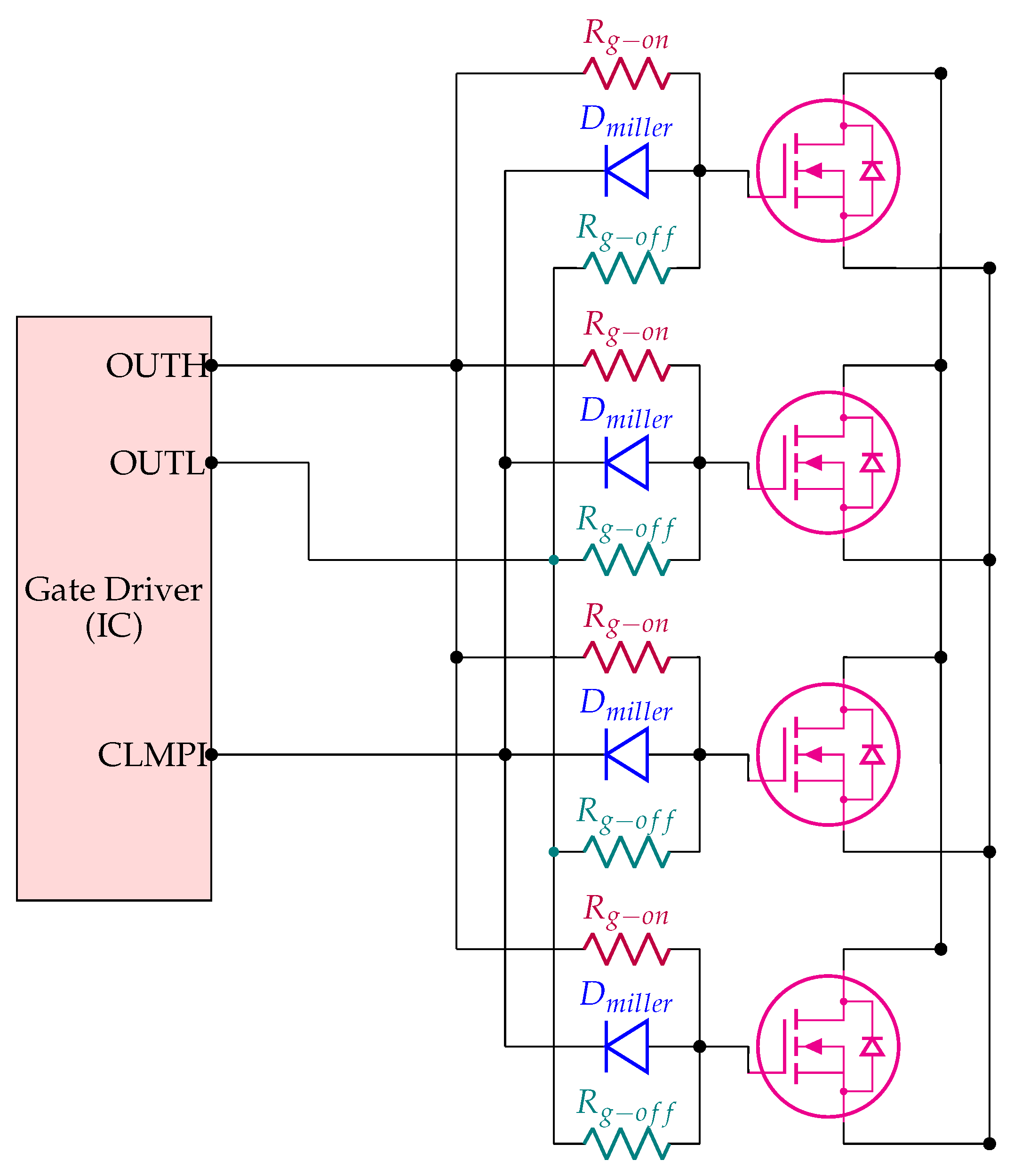
A high d V / d t causes a Miller current to flow through the Miller capacitance ( C g d ) during switching. The Miller current becomes dangerous while switching off the MOSFET because the current caused by high d V / d t increases the gate voltage. As a result, the Miller current can cause hazardous damage to the switches, such as a false turn-on and shoot-through. To avoid that, Active Miller Clamp protection is used. Basically, that circuit sinks the excessive Miller current and allows the gate voltage to remain constant. The selected gate driver circuit has this feature. However, the Active Miller Clamp protection pin of the gate driver integrated circuit ‘CLMPI’ cannot directly connect the gate of the parallel connected MOSFETs due to the interference between switches. Because any ringing of the gate voltage of any of the parallel-connected MOSFETs will reflect that to the other MOSFETs, which will result in a gate voltage ringing for all parallel-connected MOSFETs. To decrease the interference between the MOSFETs, the diodes are placed separately between the gate of the parallel-connected MOSFETs and the CLMPI pin of the gate driver integrated circuit, shown in Figure 5. A diode is preferred to the resistor because the voltage drop on the diode does not change substantially with respect to the current flow. It is important that, while the Miller current is sinking [21], the gate voltage of the MOSFET must not increase due to the voltage drop on the diode in order not to cause a false turn-on. Additionally, a symmetric layout is used to prevent a mismatch between parasitic elements on the Miller current path, shown in Figure 6. As a result of that, the inequality between gate voltages of the parallel connected MOSFETs is prevented while the Active Miller Clamp protection is working.

3.2. High Voltage Layout

Placing high voltage and high current paths on the printed circuit board (PCB) comes with many challenges. It increases the difficulty of the thermal and electrical design of the PCB. Furthermore, it can cause electrical interference between the low-voltage and high-voltage sides of the circuit. In addition, isolation and physical limitations make the design process more difficult. Therefore, a unique laminated busbar is designed to separate the high-voltage side of the circuit from the PCB. A symmetric conductor path (like in the gate driver side) instead of a laminated conductor plane is not preferred for the high voltage side of the circuit because it is very hard to design a laminated, symmetric and low parasitic inductance busbar. The laminated busbar is shown in Figure 7, which comprises three laminated layers from top to bottom; positive, negative, and output layer, respectively. The positive and negative sides of the DC voltage are laminated on the busbar to decrease parasitic inductance. The output layer refers to the midpoint of the half-bridge circuit. DC source and load connections are provided by the screw holes on the busbar. All layers of the laminated busbars have many discrete thin legs to provide a discrete connection for every discrete parallel connected MOSFET and DC-Link capacitor on the PCB. These legs are easily soldered on the vias on the PCB. Current sharing of the devices is provided on the busbar through these discrete connections. This method provides a low parasitic inductance, better thermal performance and ease of mount.

4. Experimental Verification

In this part, the experiments and test setup are explained in detail. The printed circuit test board is given in the test setup. Furthermore, the measurement devices and measurement points are also explained. Then, experimental tests and results are described. The current sharing performance and switching characteristics of parallel connected discrete SiC MOSFETs are examined.

4.1. Test Setup

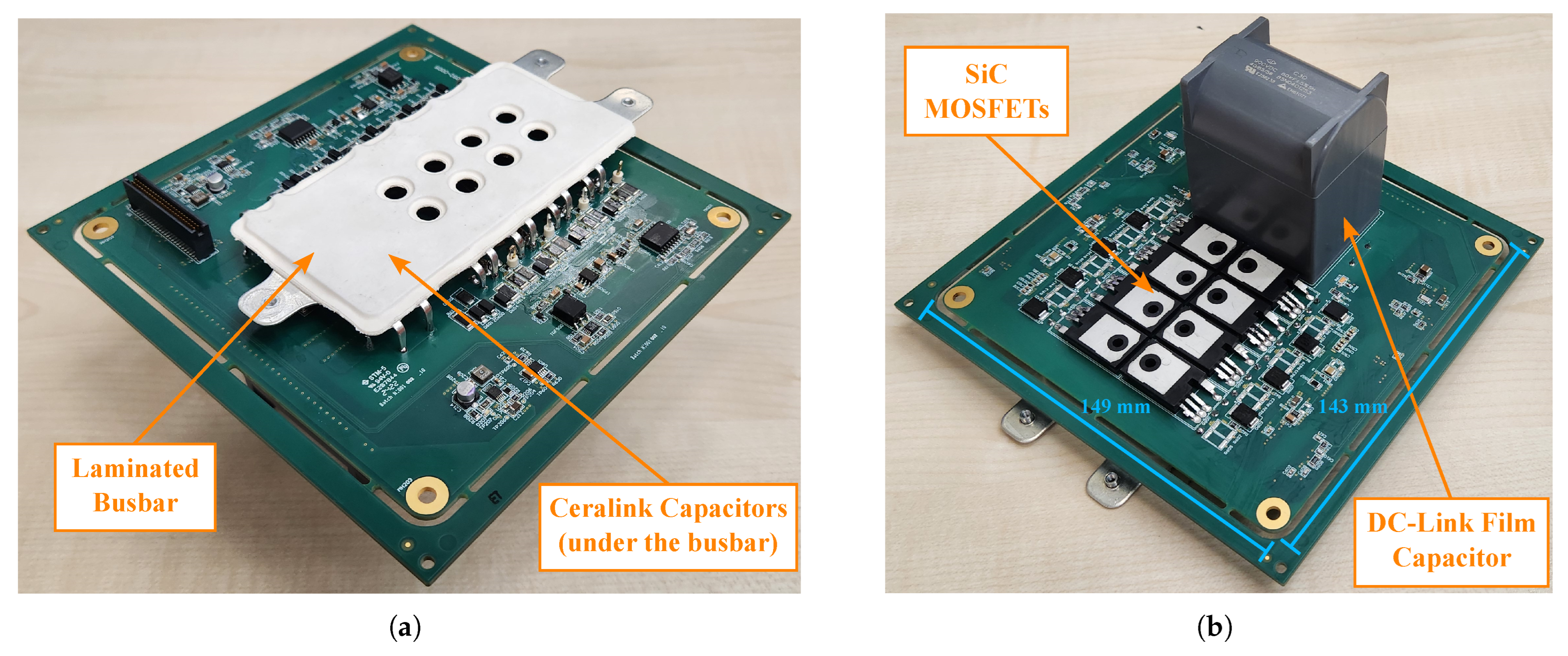
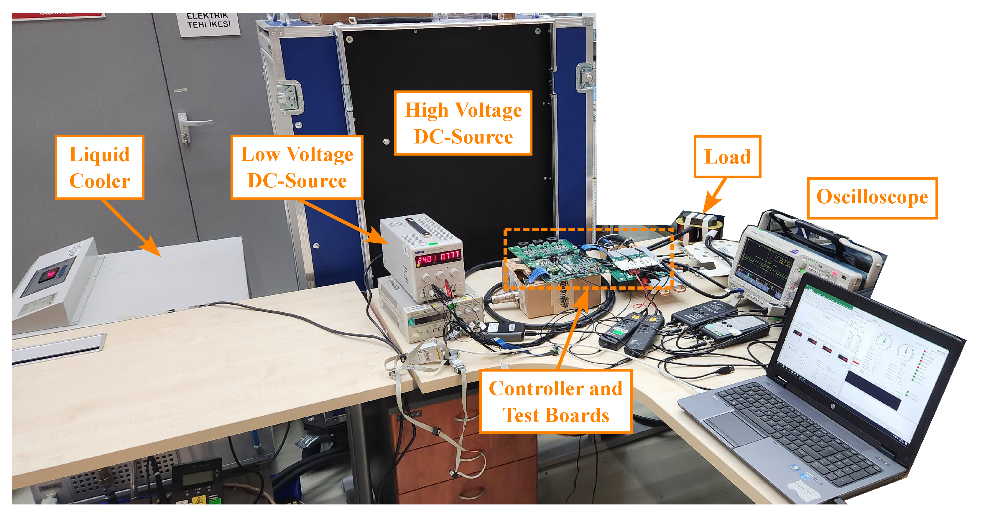
The double-pulse test circuit without a resistive load, as seen in Figure 1, is constructed for experiments. Four WolfSpeed Cree-C3M0015065K SiC MOSFETs [14] with 10 Ω gate resistance are connected in parallel for both sides of the half-bridge circuit. 220 μ H inductor is used as a load. 80 μ F film capacitor and 8 μ F Ceralink capacitors [22] are used as a DC-Link capacitance. The top side and bottom side of the laminated busbar implemented printed circuit test board can be seen in Figure 8a,b, respectively. A liquid cooling system is used to cool down the MOSFETs. Experiments are carried out for the 300 V DC-Link voltage and 50 A I d s current per MOSFET. For measurements, Tektronix MDO 3034 oscilloscope is used with the following probes: Tektronix TRCP0300 Rogowski Coil (300 A-20 mV/A), CWT-PEM Rogowski Coil (300 A-20 mV/A), Tektronix TMDP0200 (75 V p k ), Tektronix THDP0200 (1500 V p k ). Currents of two MOSFETs which are farthest from each other are measured to observe the worst case of current mismatch. Tektronix TMDP0200 (75 V p k ) is used to measure the V g s voltage and Tektronix THDP0200 (1500 V p k ) is used to measure the V d s voltage of the MOSFETs. The established test setup can be seen in Figure 9.

4.2. Experimental Results

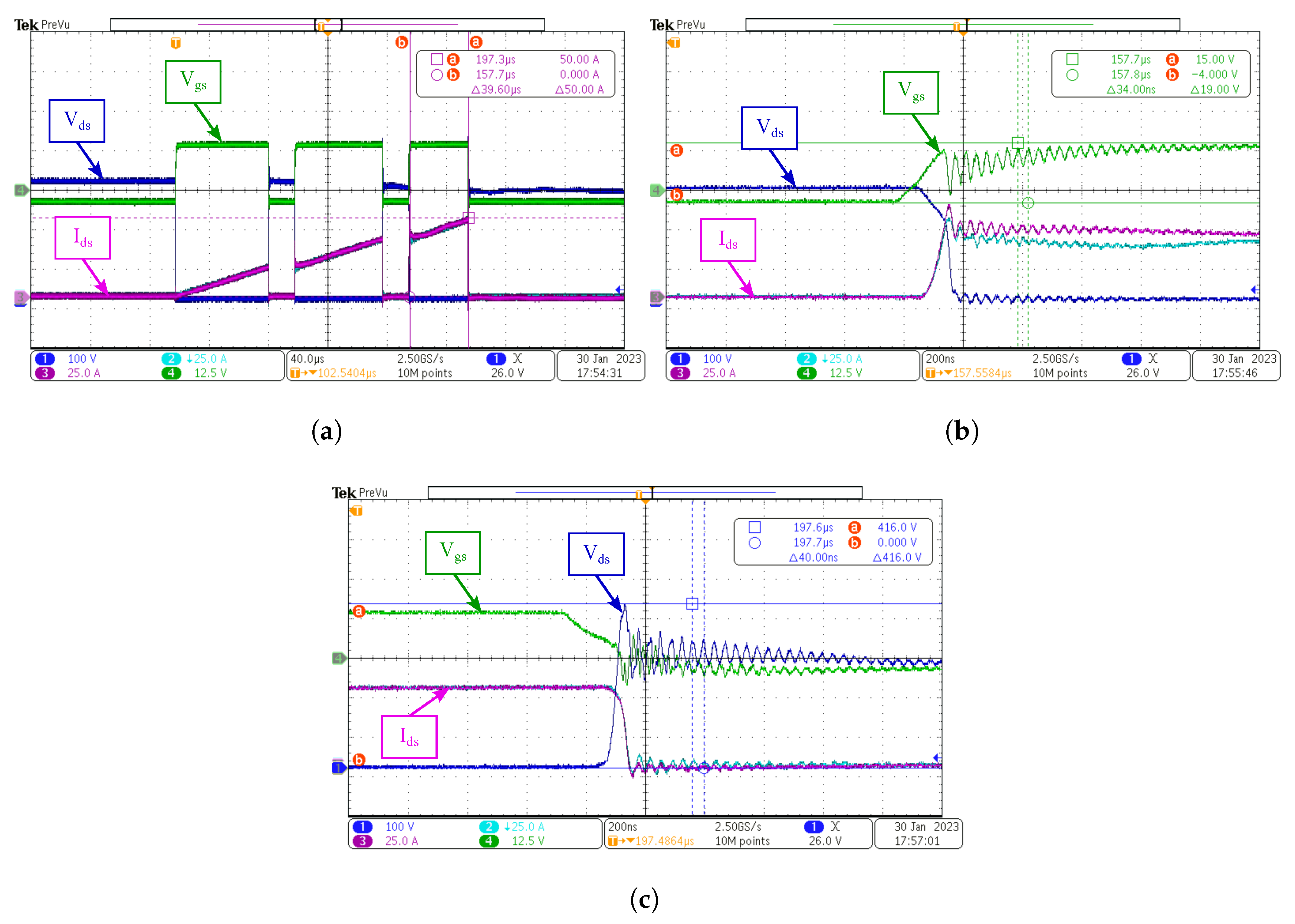
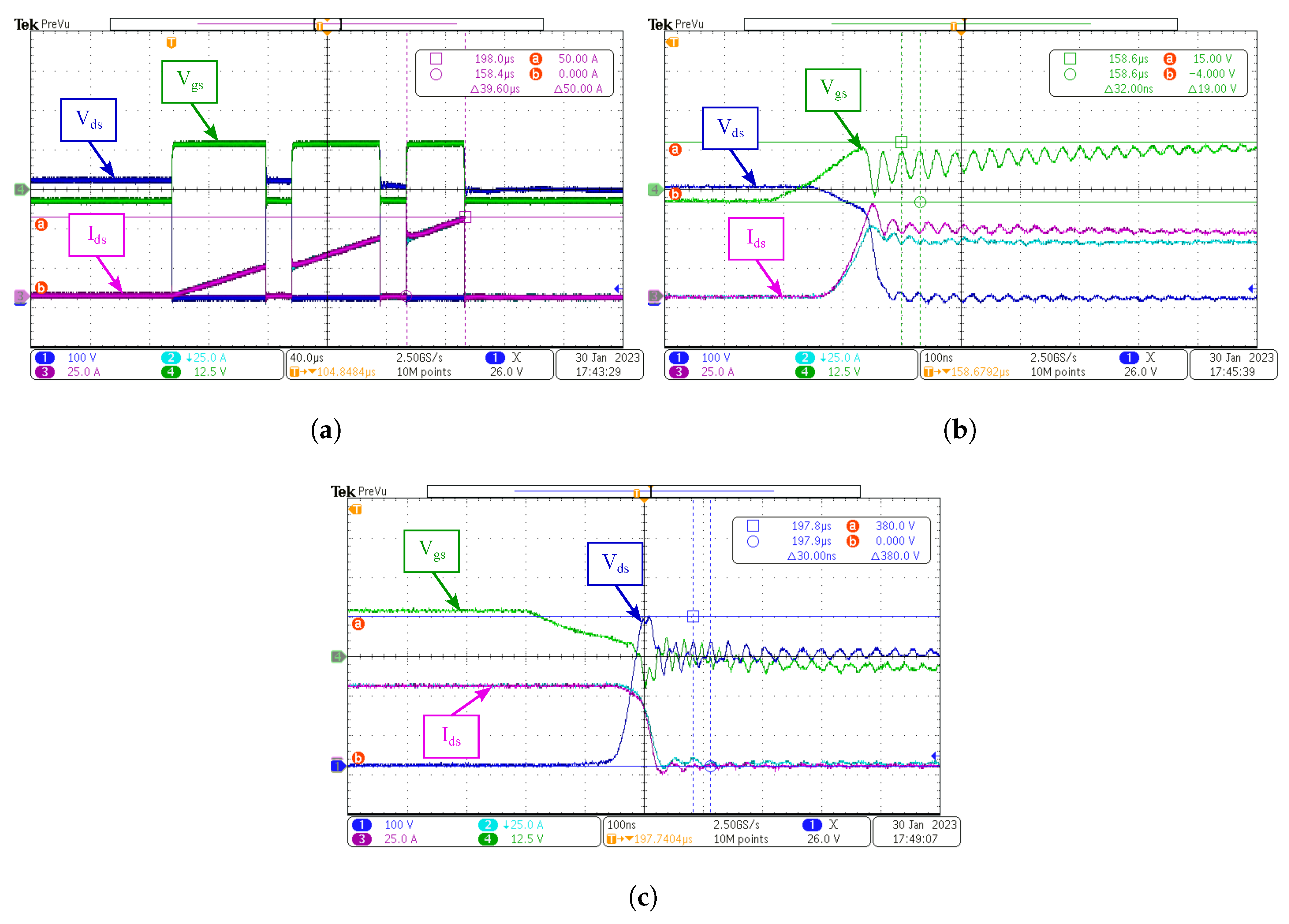
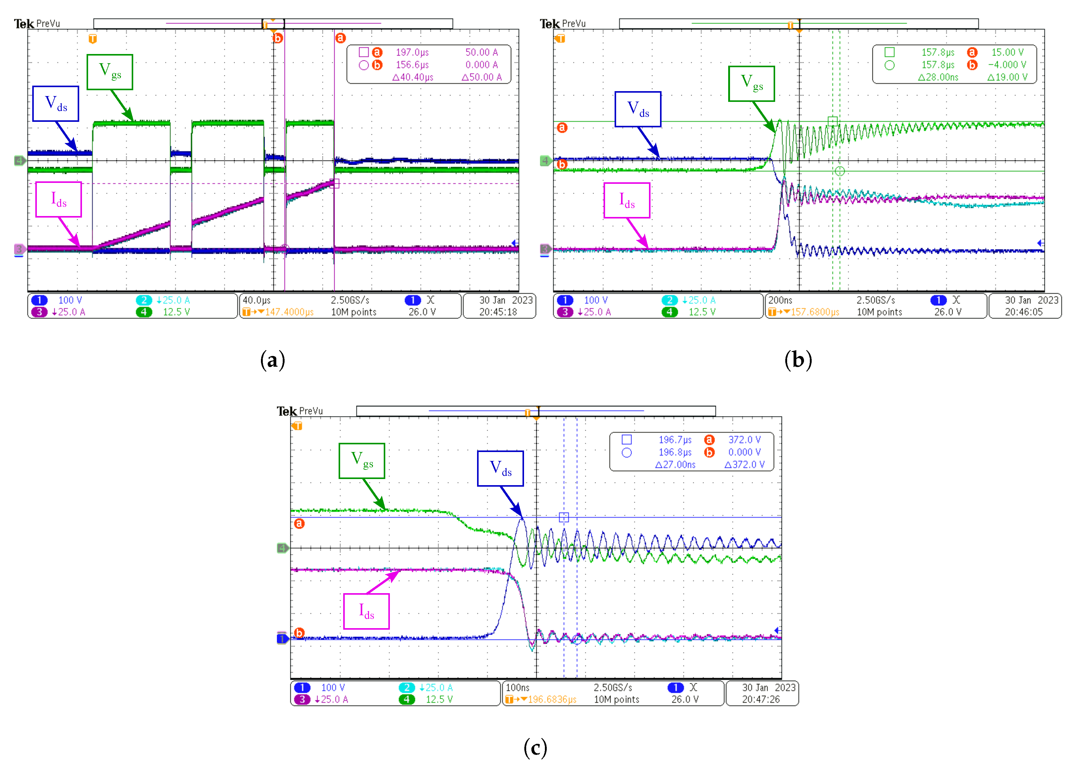
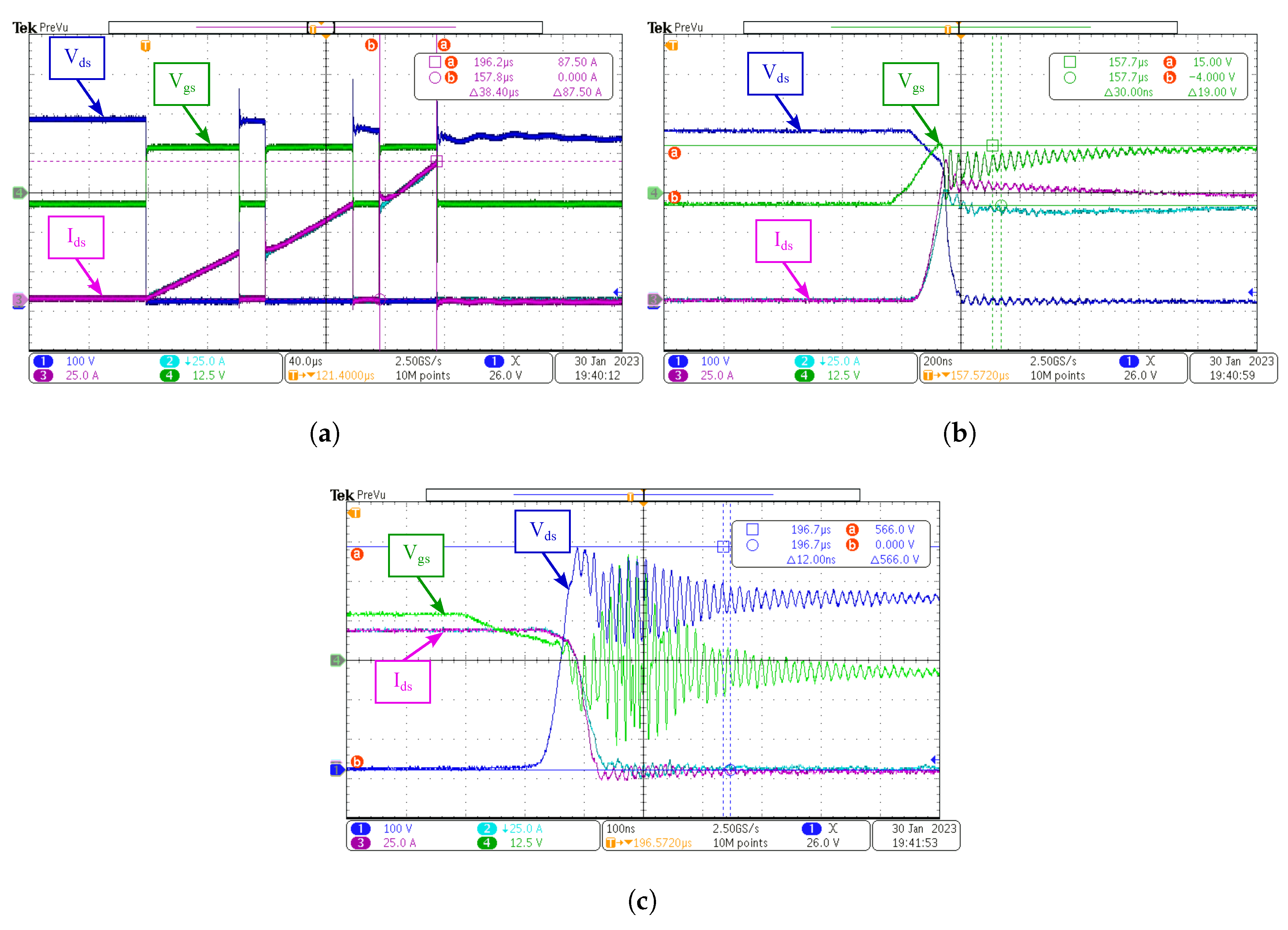
Several experimental tests were carried out to examine circuit performance. For the described test setup, approximately equal current sharing is achieved; on the other hand, the drain-source voltage overshoot problem appeared. A triple pulse is applied instead of a double-pulse to observe the higher voltage overshoot with increasing the load current. For all-scope measurement, the green waveform implies the V g s voltage, the blue waveform implies the V d s voltage, and the cyan and purple waveforms imply the I d s current of two furthest MOSFETs.
Experimental tests were carried out by changing the Ceralink capacitance [22] value and position to overcome the overshoot problem of the drain-source voltage. Three different cases were compared, where these are:
  • 2 μ F Ceralink capacitance on PCB
  • 2 μ F Ceralink capacitance on PCB + 6 μ F Ceralink capacitance located on the DC-Link input of busbar
  • 2 μ F Ceralink capacitance on PCB + 6 μ F Ceralink capacitance located through discrete MOSFETs connected in parallel.
For case-3, 6 μ F Ceralink capacitance located through discrete MOSFETs connected in parallel is shown in Figure 10. Red capacitors imply the 1 μ F Ceralink capacitor. A total of 6 μ F capacitance is distributed through discrete MOSFETs connected in parallel.
The behavior of the maximum voltage overshoot that appeared in the first case is similar to the simulation. The applied triple pulse test waveform is shown in Figure 11a. Zoomed maximum current scope images for the turn-on and turn-off cases are shown in Figure 11b,c, respectively. As seen in the results, 38% voltage overshoot occurred, which is similar to the simulation. In the second case, 6 μ F Ceralink capacitances [22] are located on the DC-Link input of the busbar. Copper sheets are used for the implementation. This improvement provides that voltage overshoot is decreased to 26%. Scope images of the applied pulse waveform, turn-on, and turn-off cases can be seen in Figure 12.
For the last case, distributed arrangement of the capacitors, connections of the capacitors are provided with the copper sheet. The voltage overshoot decreases to 24% with this improvement. The scope images of the applied pulse waveform, turn-on, and turn-off cases can be seen in Figure 13.
The maximum 460 V DC-Link voltage is tested in this setup. 87.5 A load current passed per MOSFET, a total of 350 A load current is passed in the circuit. 23% voltage overshoot is observed. Scope images of the applied pulse waveform, turn-on, and turn-off cases can be seen in Figure 14. An increase in the ringing for the turn-off case is caused by the high-voltage DC source. 350 A is a little higher than its current rating. The results of the experimental tests from the voltage overshoot point of view are shown in Table 6.
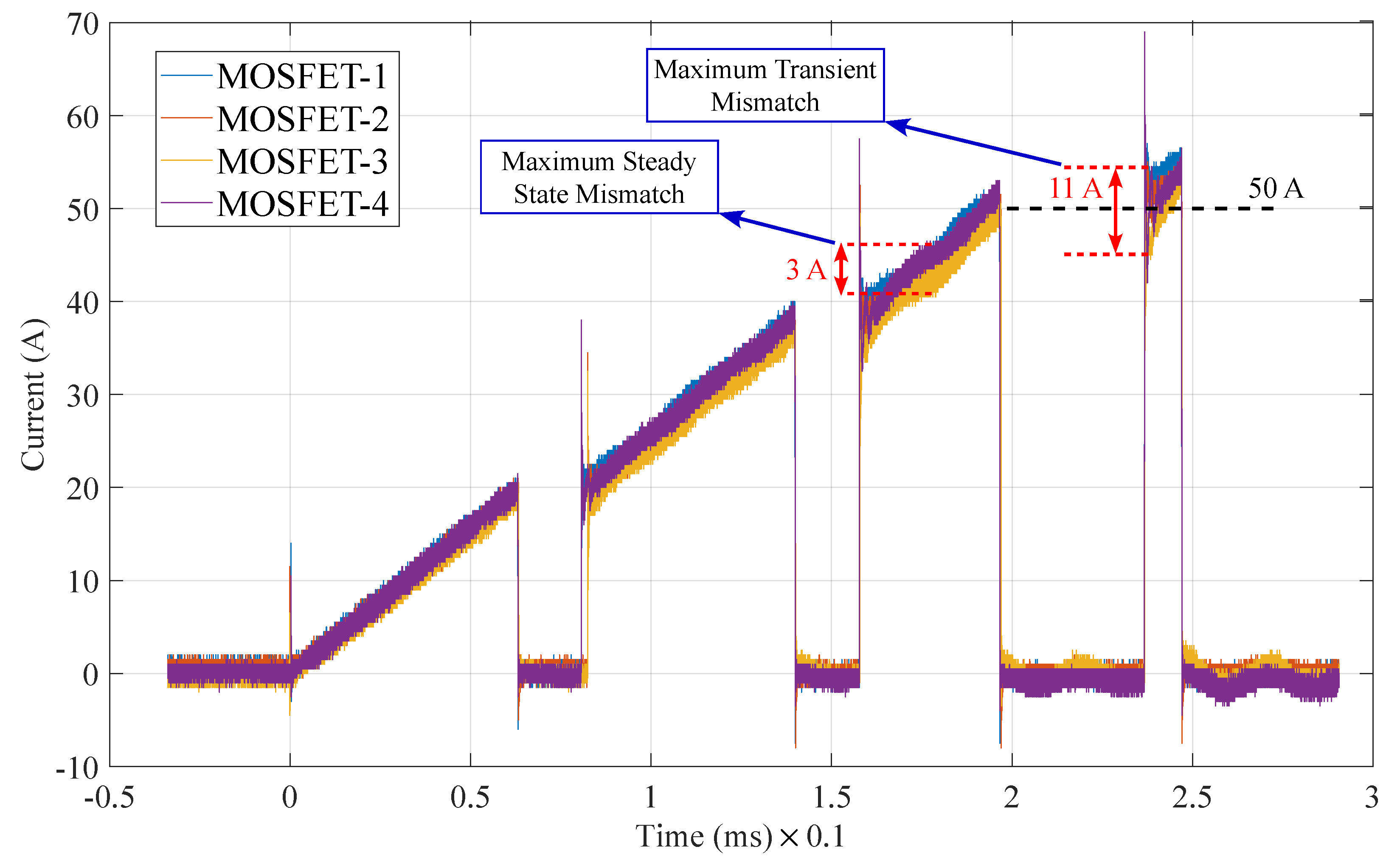
Parallel connected SiC MOSFET currents for the discretely located capacitance case are shown in Figure 15. The observed maximum steady-state current mismatch is 3 A, and the maximum transient current mismatch is 11 A. The observed maximum current mismatch is approximately 20%. Switching losses of the paralleled SiC MOSFETs are shown in Table 7. The total loss mismatch percentage is calculated based on the average total losses of the paralleled SiC MOSFETs. The observed maximum total loss mismatch is 6.2%. Furthermore, the proposed half-bridge circuit test case and test results are shown in Table 8. These values are in the acceptable range for many applications. Finally, the advantages and limitations of the proposed method are summarized in Table 9. There is no need for the active gate driver circuit, the active current balancing circuit, the passive filter, and complex calculations with the help of this method.

5. Conclusions

In this article, it was explained why the parallel connection is needed for the discrete SiC MOSFETs instead of the modules. Additionally, the technical challenges of parallel connection of SiC MOSFETs were explained briefly. In the simulation model section, the MATLAB®/Simulink® Simscape model of the Wolfspeed CREE C3M0015065K SiC MOSFET [14] was explained in detail. Furthermore, the simulation model was verified by comparing the switching losses via the double-pulse test circuit. The observed maximum loss mismatch is smaller than 10%. Moreover, a half-bridge circuit with four paralleled SiC MOSFET was constructed in the simulation program, and equal current sharing was shown; however, the voltage overshot problem occurred. A 36% overshoot was observed in the simulation. In the hardware design, the gate driver design, layout improvements, and laminated busbar model were shown in detail. The required gate driver current was calculated at approximately 10 A. The same voltage overshoot problem faced in the simulation program also appeared in the experimental test setup. The voltage overshoot decreased from 38% to 24% with an applied capacitor-based solution method. The results show that the maximum current mismatch is 6% for steady-state and 22% for transient with the described experimental setup. Additionally, this method has many advantages with the circuit size, with no active circuit and no big passive filter requirements. However, the effect on the voltage overshoot of the geometry and material type of the busbar can be further investigated. Moreover, symmetric and non-symmetric layout effects on the current mismatch can also be further investigated.

Author Contributions

Conceptualization, I.S. and S.B.O.; methodology, I.S. and S.B.O.; software, I.A.; validation, I.A., I.S. and S.B.O.; formal analysis, I.A.; investigation, I.S.; resources, I.A., I.S. and S.B.O.; data curation, I.A.; writing—original draft preparation, I.A. and S.B.O.; writing—review and editing, I.A., I.S. and S.B.O.; visualization, I.A., S.B.O.; supervision, I.S. and S.B.O.; project administration, I.S. and S.B.O.; funding acquisition, I.A. and I.S. All authors have read and agreed to the published version of the manuscript.

Funding

This research was funded by ASELSAN Inc.

Data Availability Statement

Data is contained within the article.

Conflicts of Interest

The authors declare no conflict of interest.

References

  1. Iannaccone, G.; Sbrana, C.; Morelli, I.; Strangio, S. Power Electronics Based on Wide-Bandgap Semiconductors: Opportunities and Challenges. IEEE Access 2021, 9, 139446–139456. [Google Scholar] [CrossRef]
  2. Yu, S.; Wang, J.; Zhang, X.; Liu, Y.; Jiang, N.; Wang, W. The Potential Impact of Using Traction Inverters With SiC MOSFETs for Electric Buses. IEEE Access 2021, 9, 51561–51572. [Google Scholar] [CrossRef]
  3. Xue, Y.; Lu, J.; Wang, Z.; Tolbert, L.M.; Blalock, B.J.; Wang, F. Active compensation of current unbalance in paralleled silicon carbide MOSFETs. In Proceedings of the 2014 IEEE Applied Power Electronics Conference and Exposition—APEC 2014, Fort Worth, TX, USA, 16–20 March 2014; pp. 1471–1477. [Google Scholar] [CrossRef]
  4. Xue, Y.; Lu, J.; Wang, Z.; Tolbert, L.M.; Blalock, B.J.; Wang, F. A compact planar Rogowski coil current sensor for active current balancing of parallel-connected Silicon Carbide MOSFETs. In Proceedings of the 2014 IEEE Energy Conversion Congress and Exposition (ECCE), Pittsburgh, PA, USA, 14–18 September 2014; pp. 4685–4690. [Google Scholar] [CrossRef]
  5. Wen, Y.; Yang, Y.; Gao, Y. Active Gate Driver for Improving Current Sharing Performance of Paralleled High-Power SiC MOSFET Modules. IEEE Trans. Power Electron. 2021, 36, 1491–1505. [Google Scholar] [CrossRef]
  6. Lu, S.; Deng, X.; Li, S.; Rong, E. A Passive Transient Current Balancing Method for Multiple Paralleled SiC-MOSFET Half-Bridge Modules. In Proceedings of the 2019 IEEE Applied Power Electronics Conference and Exposition (APEC), Anaheim, CA, USA, 17–21 March 2019; pp. 349–353. [Google Scholar] [CrossRef]
  7. Li, H.; Zhou, W.; Wang, X.; Munk-Nielsen, S.; Li, D.; Wang, Y.; Dai, X. Influence of Paralleling Dies and Paralleling Half-Bridges on Transient Current Distribution in Multichip Power Modules. IEEE Trans. Power Electron. 2018, 33, 6483–6487. [Google Scholar] [CrossRef]
  8. Mao, Y.; Miao, Z.; Wang, C.M.; Ngo, K.D.T. Balancing of Peak Currents Between Paralleled SiC MOSFETs by Drive-Source Resistors and Coupled Power-Source Inductors. IEEE Trans. Ind. Electron. 2017, 64, 8334–8343. [Google Scholar] [CrossRef]
  9. Zeng, Z.; Zhang, X.; Zhang, Z. Imbalance Current Analysis and Its Suppression Methodology for Parallel SiC MOSFETs with Aid of a Differential Mode Choke. IEEE Trans. Ind. Electron. 2020, 67, 1508–1519. [Google Scholar] [CrossRef] [Green Version]
  10. Ahmed, M.R.; Todd, R.; Forsyth, A. Analysis of SiC MOSFETs under hard and soft-switching. In Proceedings of the IEEE Energy Conversion Congress and Exposition (ECCE), Virtual, 10–14 October 2015; pp. 2231–2238. [Google Scholar]
  11. Yuan, D.; Zhang, Y.; Wang, X.; Gao, J. A Detailed Analytical Model of SiC MOSFETs for Bridge-Leg Configuration by Considering Staged Critical Parameters. IEEE Access 2021, 9, 24823–24847. [Google Scholar] [CrossRef]
  12. Wei, Y.; Mantooth, A. Subcircuit Based Modelling of SiC MOSFET in MATLAB/SIMULINK. In Proceedings of the IEEE 12th Energy Conversion Congress & Exposition Asia (ECCE-Asia), Singapore, 24–27 May 2021; pp. 2339–2344. [Google Scholar] [CrossRef]
  13. Plotdigitizer. Available online: https://plotdigitizer.com/app (accessed on 20 April 2022).
  14. Wolfspeed CREE SiC MOSFET C3M0015065K. Available online: https://assets.wolfspeed.com/uploads/2020/12/C3M0015065K.pdf (accessed on 6 March 2022).
  15. Mao, S.; Popovic, J.; Ferreira, J.A. Switching Characterization and Low Inter-winding Capacitance Gate Driver Power Supply of 1200 V SIC MOSFET for the 300 kHz 10 kW Inverter. In Proceedings of the 1st Workshop Wide Bandgap Power Devices Applications Asia (WiPDA Asia), Xi’an, China, 16–18 May 2018; pp. 270–275. [Google Scholar] [CrossRef]
  16. Li, S.T.; Wang, P.Y.; Chen, C.J.; Hsu, C.C. A 10 MHz GaN Driver with Gate Ringing Suppression and Active Bootstrap Control. In Proceedings of the IEEE Workshop Wide Bandgap Power Devices Applications Asia (WiPDA Asia), Taipei, Taiwan, 23–25 May 2019; pp. 1–4. [Google Scholar]
  17. Concept. Application Note AN-1001. Available online: https://www.power.com/sites/default/files/documents/AN-1001_IGBT_and_MOSFET_Drivers_Correctly_Calculated.pdf (accessed on 20 July 2022).
  18. Qu, J.; Zhang, Q.; Yuan, X.; Cui, S. Design of a paralleled SiC MOSFET half-bridge unit with distributed arrangement of DC capacitors. IEEE Trans. Power Electron. 2020, 35, 10879–10891. [Google Scholar] [CrossRef]
  19. Zhu, Y.; Huang, Y.; Wu, H.; Din, Z.; Zhang, J. A Multi-Level Gate Driver for Crosstalk Suppression of Silicon Carbide MOSFETs in Bridge Arm. IEEE Access 2021, 9, 100185–100196. [Google Scholar] [CrossRef]
  20. Wang, G.; Mookken, J.; Rice, J.; Schupbach, M. Dynamic and static behavior of packaged silicon carbide MOSFETs in paralleled applications. In Proceedings of the 2014 IEEE Applied Power Electronics Conference and Exposition—APEC 2014, Fort Worth, TX, USA, 16–20 March 2014; pp. 1478–1483. [Google Scholar] [CrossRef]
  21. Aeloiza, E.; Kadavelugu, A.; Rodrigues, R. Novel Bipolar Active Miller Clamp for Parallel SiC MOSFET Power Modules. In Proceedings of the 2018 IEEE Energy Conversion Congress and Exposition (ECCE), Portland, OR, USA, 23–27 September 2018; pp. 401–407. [Google Scholar] [CrossRef]
  22. Ceralink Capacitor. Available online: https://product.tdk.com/en/search/capacitor/ceramic/ceralink/info?part_no=B58031U5105M062 (accessed on 10 March 2022).
Figure 1. Proposed half-bridge topology with four paralleled SiC MOSFETs.
Energies 16 02903 g001
Figure 2. Double−pulse test (DPT) circuit.
Energies 16 02903 g002
Figure 3. Simulation results, (a) applied waveform, (b) turn-on waveform, (c) turn-off waveform.
Energies 16 02903 g003aEnergies 16 02903 g003b
Figure 4. Layout of the gate driver circuit, (a) Gate turn-on path “yellow trace”, (b) gate turn-off path “blue trace”.
Energies 16 02903 g004aEnergies 16 02903 g004b
Figure 5. Schematic of Active Miller Clamp protection.
Energies 16 02903 g005
Figure 6. Layout of the Active Miller Clamp protection.
Energies 16 02903 g006
Figure 7. Laminated busbar.
Energies 16 02903 g007
Figure 8. PCB images, (a) top side of the PCB, (b) bottom side of the PCB.
Energies 16 02903 g008
Figure 9. Experimental test setup.
Energies 16 02903 g009
Figure 10. Location of 6 μ F Ceralink capacitance connected in parallel through discrete MOSFETs.
Energies 16 02903 g010
Figure 11. 2 μ F Ceralink capacitance on PCB, (a) Triple pulse test waveform, (b) Gate−source voltage waveform, (c) Drain−source voltage waveform.
Energies 16 02903 g011
Figure 12. Extra 6 μ F Ceralink capacitance located on the DC−Link input of busbar, (a) Triple pulse test waveform, (b) Gate−source voltage waveform, (c) Drain−source voltage waveform.
Energies 16 02903 g012
Figure 13. Extra 6 μ F Ceralink capacitance located through discrete MOSFETs connected in parallel, (a) Triple pulse test waveform, (b) Gate−source voltage waveform, (c) Drain−source voltage waveform.
Energies 16 02903 g013
Figure 14. Maximum DC−link voltage case, (a) Triple pulse test waveform, (b) Gate−source voltage waveform, (c) Drain−source voltage waveform.
Energies 16 02903 g014
Figure 15. Paralleled SiC MOSFET currents.
Energies 16 02903 g015
Table 1. SiC MOSFET body diode I d s current with respect to the V g s & V d s voltages at 25 °C.
Ids (A) Vds (V)
Vgs (V)−10−9−8−7−6−5−4−3−2−10
−4−444−356−268−180−92−39−11−0.9−0.001−0.00010
Table 2. First quadrant SiC MOSFET I d s current with respect to the V g s & V d s voltages at 25 °C.
Ids (A) Vds (V)
Vgs (V)012345678910
15065127185243301359417475533591
13057107154197240283326369412455
1104481114143170194216238260282
1003665.591113132.5149.5165179.5193.5207
902850688395105114121127132
70132127313437387394142
509.281519.2822.1424.2826.4227.1427.8529.2830
000000000000
−0.00100000000000
−800000000000
Table 3. Third quadrant SiC MOSFET I d s current with respect to the V g s & V d s voltages at 25 °C.
Ids (A) Vds (V)
Vgs (V)−10−9−8−7−6−5−4−3−2−10
15−817−734−651−568−485−402−319−236−153−700
13−803.4−720.4−637.4−554.4−471.4−388.4−305.4−222.4−139.4−620
11−789.8−706.8−623.8−540.8−457.8−374.8−291.8−208.8−125.8−540
10−783−700−617−534−451−368−285−202−119−500
9−734−656−578−500−422−344−266−188−107.2−430
7−636−568−500−432−364−296−228−160−83.6−290
5−538−480−422−364−306−248−190−132−60−150
0−464−395−326−257−188−119−69−34−2.7−0.30
−0.00100000000000
−800000000000
Table 4. SiC MOSFET capacitance table for V d s voltage at 25 °C.
Vds (V)
C (pF)031012.520304050100150200300400500600640
C iss 6570571152845122512251225202520252025202512249754975489748974897
C oss 52023313201315221205969816744528431381303289289289285
C rss 18348043261381007865584336322727282828
Table 5. SiC MOSFET SW loss comparison table at 25 °C.
SW Loss(Datasheet)SW Loss(Simulation)Total Loss
Ids (A) E on ( μ J) E off ( μ J) E on ( μ J) E off ( μ J)Error (%)
3023195209.599.285.28
40287156286.1168.42.59
60416316468.3305.35.68
70488406577.2379.97.05
Table 6. V d s overshoot comparison table.
CaseIds (A)Switching Voltage (V)Overshoot Voltage (V)Overshoot (%)
Case-15030041638
Case-25030038026
Case-35030037224
Case-Max.87.546056623
Table 7. Switching loss comparison.
MOSFET E on ( μ J) E off ( μ J)Total Loss ( μ J)Total Loss Mismatch (%)
MOSFET-14065629683.12
MOSFET-24065629683.12
MOSFET-34375629990.025
MOSFET-450056210626.27
Table 8. Proposed half-bridge circuit results.
CaseVoltage (V)Current (A)Voltage Overshoot (%)Maximum Current Mismatch (%)Total Switching Loss Mismatch (%)
Discrete Located Capacitor3005024226.27
Table 9. Proposed half-bridge circuit advantages and limitations.
AdvantagesLimitations
No active gate driverLaminated busbar required
No active current balance circuitCircuit parasitics depend on the busbar and PCB design
No big passive filter circuit
No complex calculation
Easy to implement
Disclaimer/Publisher’s Note: The statements, opinions and data contained in all publications are solely those of the individual author(s) and contributor(s) and not of MDPI and/or the editor(s). MDPI and/or the editor(s) disclaim responsibility for any injury to people or property resulting from any ideas, methods, instructions or products referred to in the content.