Article

An Improved Delayed Signal Cancelation for Three-Phase Grid Synchronization with DC Offset Immunity

1
The Department of Electrical Engineering, Jordan University of Science and Technology, P.O. Box 3030, Irbid 22110, Jordan
2
The Department of Electrical Engineering, Faculty of Engineering, University of Tabuk, P.O. Box 741, Tabuk 47512, Saudi Arabia
*
Author to whom correspondence should be addressed.
Energies 2023, 16(6), 2873; https://doi.org/10.3390/en16062873
Submission received: 16 February 2023 / Revised: 8 March 2023 / Accepted: 16 March 2023 / Published: 20 March 2023

Abstract

:
The presence of the DC components in the grid voltage adversely affects the performance of the synchronization unit, causing oscillatory and offset errors in the estimated grid information. Several approaches were proposed to address the DC offset problem by incorporating an additional filtering stage to the synchronous reference frame phase-locked loop (SRF-PLL). Removing the DC offset using the modified delayed signal cancelation (MDSC) operator in the inner loop of the SRF-PLL shows a good DC offset elimination with a fast-dynamic response. However, neither a straightforward selection procedure for the MDSC parameters nor a general estimation technique for the grid information is provided. Hence, a generalization for the MDSC is proposed in this paper based on general mathematical expressions to cancel out the DC offset, while meanwhile estimating the grid parameters precisely and rapidly against any delay factor selection. Finally, comprehensive simulation and experimental results compared with other related PLLs are presented to demonstrate the effectiveness of the proposed work.

1. Introduction

The phase-locked loop (PLL) is a negative-feedback-closed-loop control system commonly used in grid synchronization and control of grid-tied power converters [1,2,3,4]. The wide usage of power converters is due to their ability to convert electrical power from one form to another, making it possible to use power from different sources and to power different devices with different requirements. PLLs are also used in sensorless control of electrical machines [5], power quality indices [6,7], and islanding detection [8].
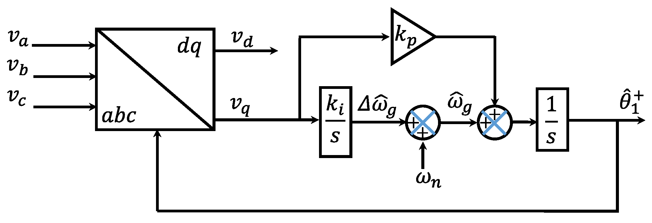
Among all types of PLL, the most common type used in the three-phase applications is the conventional synchronous reference frame (SRF)-PLL with a proportional-integral (PI) controller as a loop filter due to its structural simplicity and ease of implementation [9,10]. In the conventional SRF-PLL depicted in Figure 1, the PI controller can only mitigate the phase error and estimate the grid parameters precisely under ideal conditions. However, it cannot completely block or attenuate the harmonics, the DC offset, and any possible grid noise.
The DC offset in the grid voltage may be generated because of grid faults [11], geomagnetic phenomena [12], the A/D conversion process [13], and the DC injection by distributed generation systems, specifically PV inverters [14], to name a few. In addition, the power quality problems related to the presence of the DC components in the grid voltage adversely affect the performance of the synchronization unit, causing oscillatory and offset errors in the estimated grid information [15].
The bandwidth (BW) of the PLL must be restricted to a low value to attenuate the DC offset using the conventional SRF-PLL. This results in poor dynamic performance and may not be acceptable in most applications. For example, the requirement for settling time in common grid codes is less than two grids’ fundamental cycles [16,17].
Recently, several approaches have been proposed to incorporate an additional filtering stage, either in the inner or outer loop of the conventional SRF, to deal with the DC offset problem [17,18,19,20,21]. Besides the DC offset rejection, estimating the amplitude and the phase of the fundamental grid voltage components and compensating for the phase lead caused by those additional filters puts another challenge to be solved to synchronize with the grid perfectly.
In [18], the moving average filter (MAF) is used in the inner loop of the PLL, showing an excellent rejection capability against the harmonics. However, its dynamic response is slow, especially under the frequency drifts, which appear as ripples in the estimated frequency. Moreover, under large frequency drifts, the MAF performance becomes worse. Therefore, the estimation of the grid information is degraded.
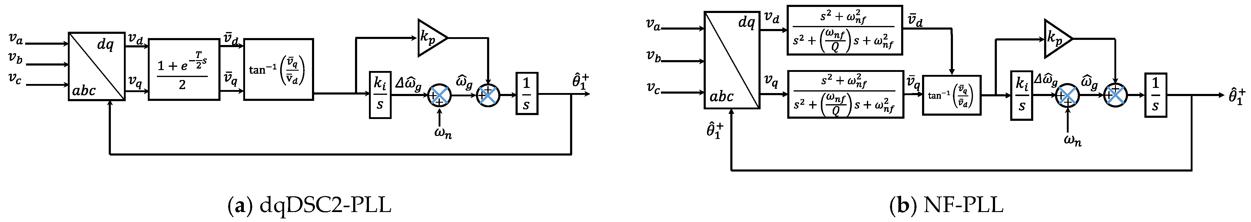
In [19], a notch filter phase-locked loop (NF-PLL) is proposed for grid synchronization with DC offset rejection technique by replacing the in-loop MAF with a notch filter. This enables the PLL to block the DC offset contaminated with the grid voltages effectively at the cost of slowing down the response. Moreover, the NF-PLL performance becomes worse under large frequency drift, which can be solved by narrowing the bandwidth of the NF; however, this adversely affects the PLL’s performance.
Delayed signal cancellation (DSC) PLL that provides good DC offset filtering capability has been proposed in [20]. The dqDSC is implemented in the PLL inner loop and has only one decisive parameter: the delay factor. Selecting a specific delay factor to eliminate the DC offset, the dqDSC shows good rejection capability, but its dynamic response is slow. The slow dynamic response caused by the DSC operator can be improved by adding a phase lead compensator in the PLL’s inner loop, which may decrease the DC rejection capability of the PLL, specifically under grid frequency drift.
In contrast, the αβDSC-PLL, implemented in the PLL outer loop, shows a good DC offset rejection capability with a faster transient response than the dqDSC-PLL under the same delayed factor. However, the phase compensation method needed under frequency deviation complicates the PLL design [21].
In [22], a specific design parameter is suggested using modified delayed signal cancelation (MDSC) in the inner loop of the SRF-PLL with a specific delay factor. The MDSC based PLL shows good DC offset elimination with rapid response. The lead-in phase caused by the MDSC operator is compensated by computing the lead-in phase and then adding the same angle directly into the PLL output, which is not general for any delay factor selection. Moreover, it does not have a general voltage amplitude estimation technique under the arbitrary delay factor.
Therefore, this paper proposes a generalization to the MDSC-PLL. The proposed PLL is based on general mathematical relationships between the delay factor and the design parameter, eliminating the DC offset and extracting the grid voltage’s fundamental frequency positive sequence (FFPS) under any delay factor. Moreover, the proposed model has simple and general estimation techniques to estimate the grid voltage amplitude, frequency, and phase.
This paper is arranged as follows: Section 2 presents an overview of DSC and MDSC operators. Then, the proposed PLL with amplitude and phase compensation formulas is derived in Section 3. In Section 4, the mathematical model is derived, and the controller gains are designed. In Section 5, with two selections of the delay factor, the justification for the proposed model and its mathematical model against both compensation formulas are implemented mathematically and throughout the numerical simulation. In 
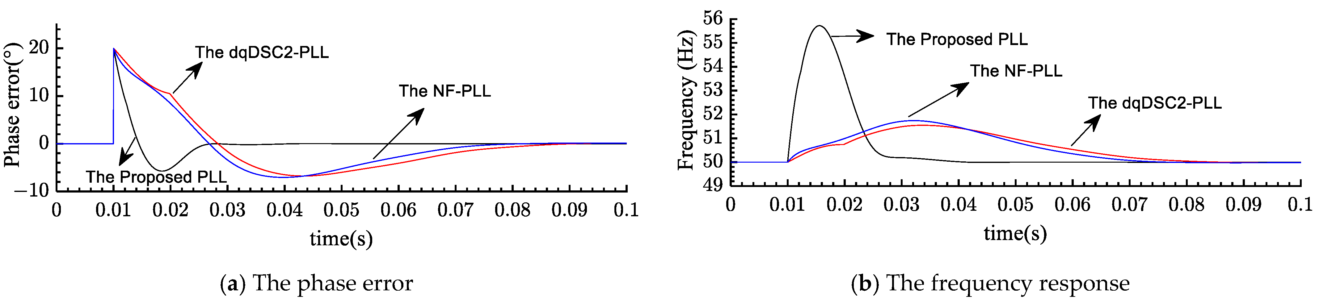
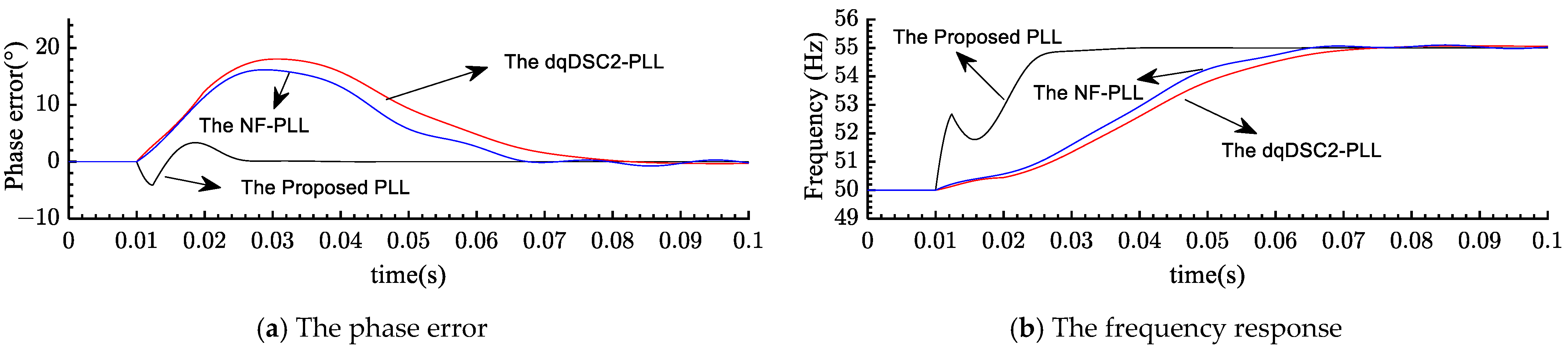
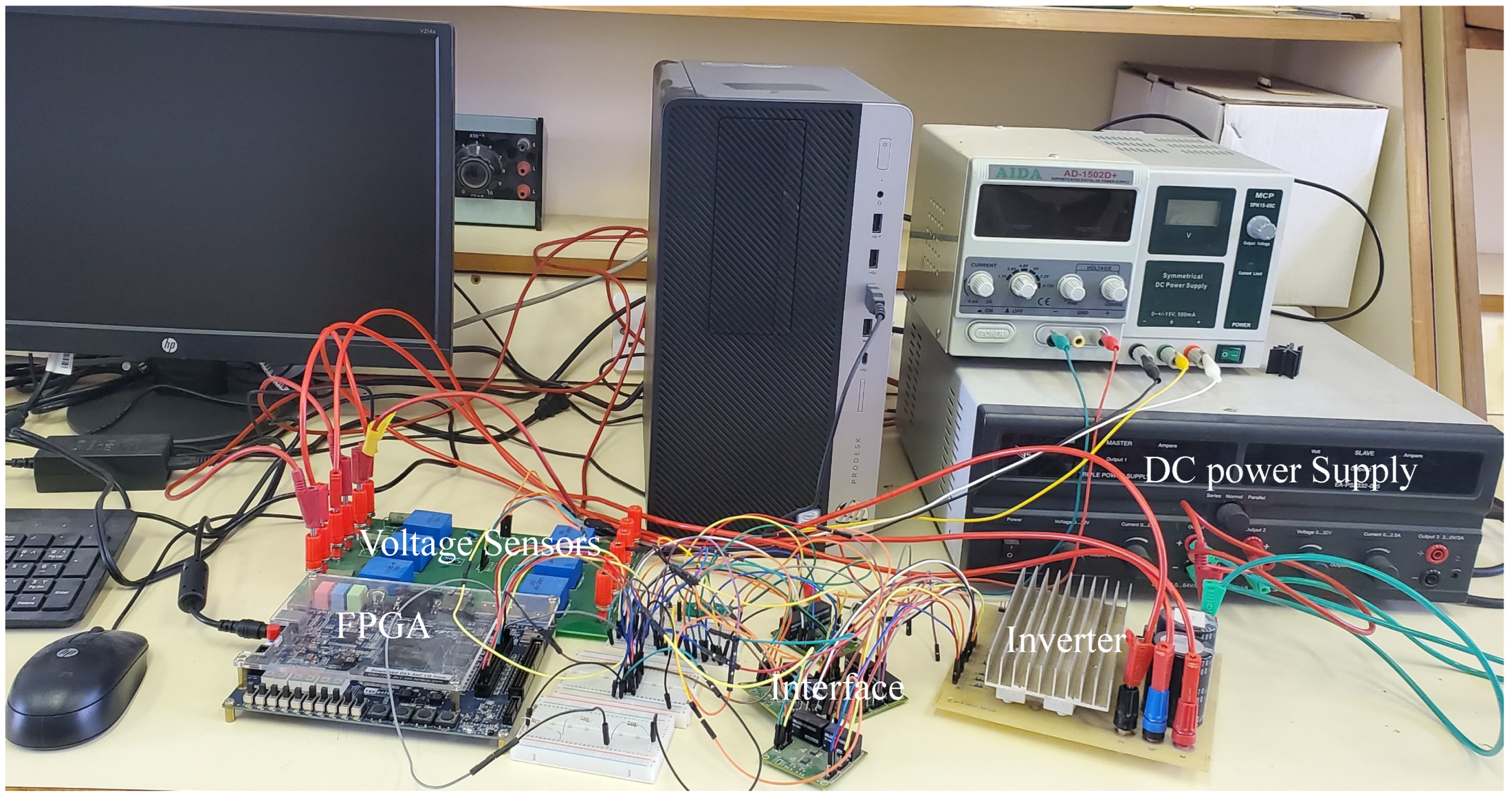
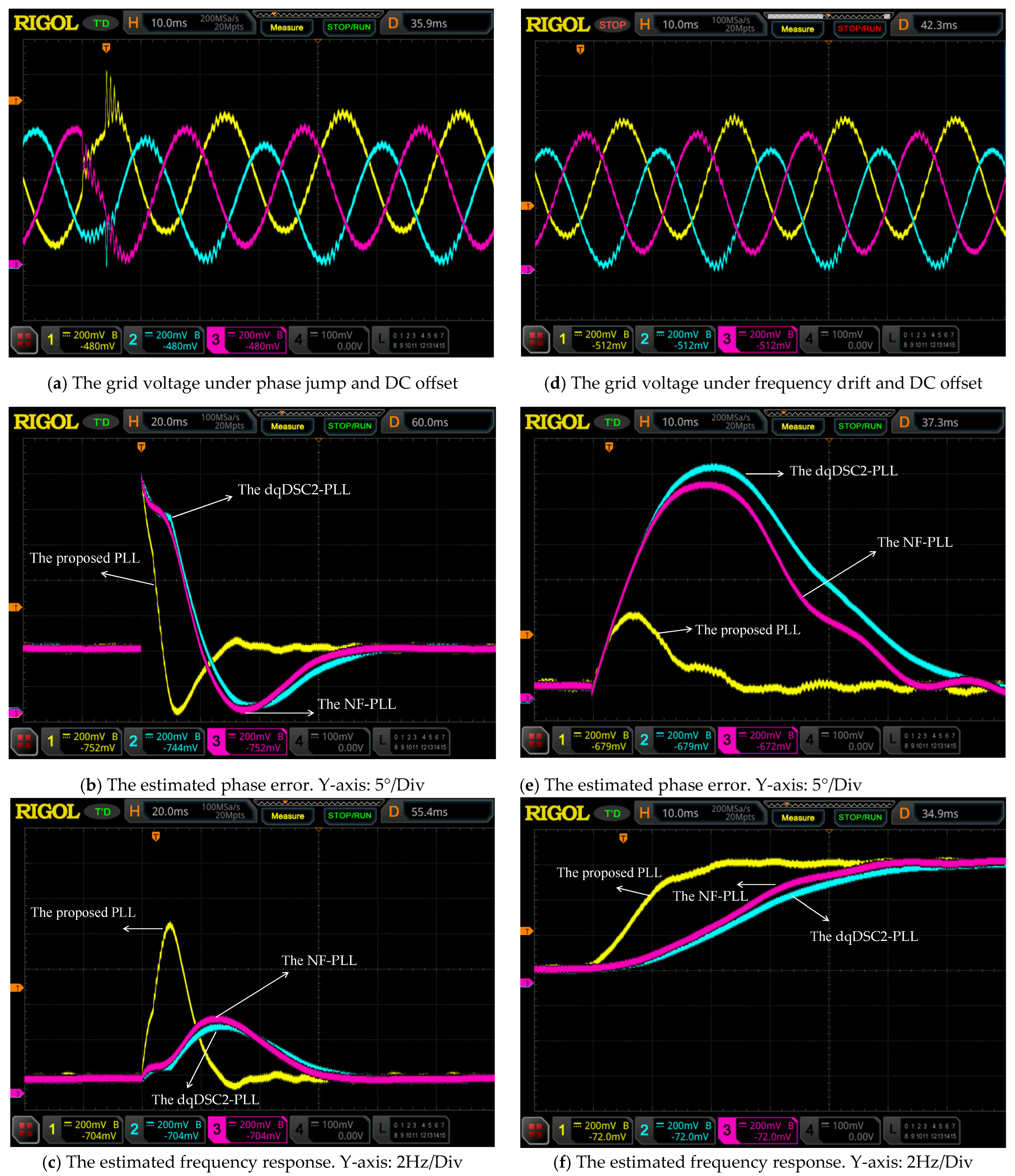
Section 6, experimental results compared with other related PLLs are presented to demonstrate the effectiveness of the proposed PLL. Finally, Section 7 concludes the paper’s findings.

2. The Modified Delayed Signal Cancellation Operator

The DC offset in the input of the synchronizing unit causes an oscillation in the estimated grid information. The DC component in the abc-reference frame has a zero-harmonic order; hence, it becomes a negative one in the dq-reference frame after using Park’s transformation. Therefore, the DC component appears as a sinusoidal wave in the dq-reference frame and possesses half-wave symmetry. A summation with the delayed versions in the dq-reference frame can cancel out the DC component, which illustrates the basic topology of the DSC operator. The DSC operator is commonly implemented in the inner loop of the PLL operating in the dq-reference frame. The general expression for the DSC operator in the s-domain can be described as:
D S C ( s ) = 1 + e T n s 2 ,
where T is the fundamental voltage grid period, and n is an integer that specifies the delay factor.
In Equation (1), the DSC operator has only one design parameter, the n. This operator is used widely in many approaches since it has excellent rejection capabilities against the DC offset and harmonics, which depends on its selection; each n has a specific ability to deal with certain harmonics. However, it suffers from slow dynamic performance when used to reject the DC component. Thus, the DSC operator is modified into the MDSC operator, giving the DSC flexibility and improving its dynamic response [22]. The MDSC operator can be expressed in the s-domain as:
M D S C ( s ) = 1 + e j 2 π n s e T n s 2 ,
where ns is a design parameter used to shift the frequency characteristics of the DSC, 
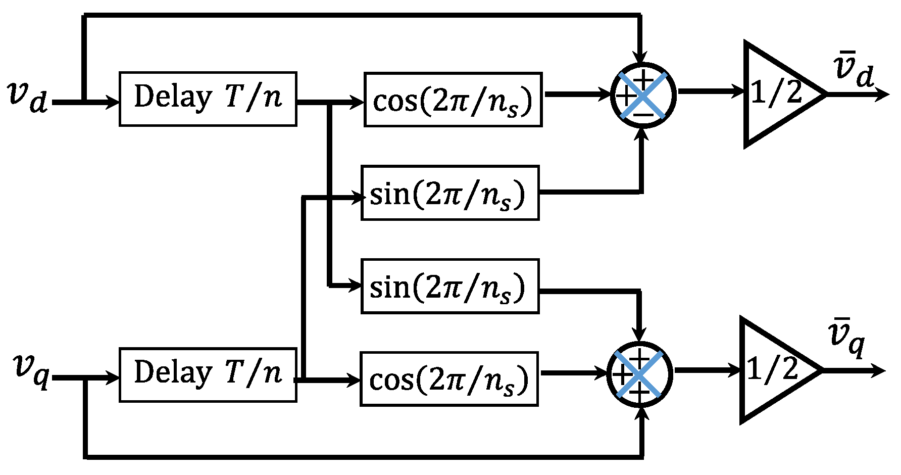
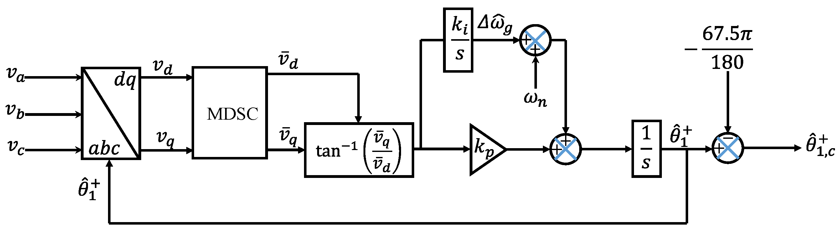
Figure 2 depicts the time-domain implementation of the MDSC operator. In contrast, the schematic diagram of the MDSC-PLL is illustrated in Figure 3 [22].

3. The Proposed Phase-Locked Loop

The MDSC-PLL features excellent dynamic performance and DC offset rejection with a shorter delay. However, it does not have an explicit general algorithm for selecting the MDSC operator’s parameters against any delay operator. Moreover, the utilized compensation criteria are based on calculating the phase lead under a specific delayed factor. Hence, the compensation in [22] is not general and hard to be adopted under an arbitrary delay factor. Moreover, no general voltage amplitude estimation is discussed in [22].
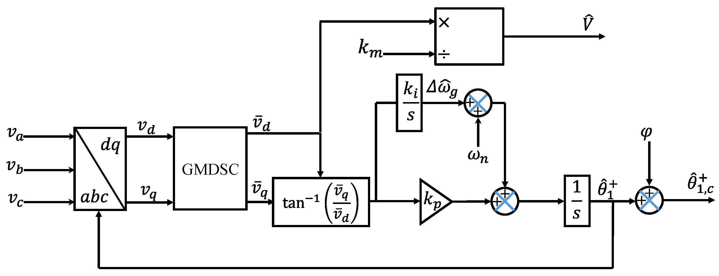
Therefore, to achieve perfect synchronization with an arbitrary delay factor, the MDSC-PLL is generalized in this paper. The proposed PLL is based on general mathematical relationships between the delay factor and the design parameter. The proposed PLL can eliminate the DC offset and extract the FFPS of the grid voltage precisely and rapidly while estimating the amplitude of the grid voltage and compensating the lead-in phase under any election of the delay factor.
To derive a general expression of the proposed PLL in the dq-reference frame under any selection of n, consider the grid voltage that contains some DC offset components:
v a v b v c = V m sin θ sin θ 2 π 3 sin θ + 2 π 3 + v a d c v b d c v c d c ,
where:  θ = ω g t + ω g = ω n + Δ ω g  and  ω n = 2 π f n . The subscript ‘ a b c ’ defines the reference frame of the grid, which is called the natural reference frame,  V m  is the grid voltage amplitude of the FFPS component,  θ  is the grid phase angle of the FFPS component,  ω g  is the grid angular frequency,  ω n  is the nominal grid fundamental angular frequency,  f n  is the nominal grid fundamental frequency, and   is the grid voltage initial phase angle,  v a d c v b d c , and  v c d c  are the DC components in the grid voltages.
Applying Park’s transformation to the grid voltage in Equation (3) yields:
v d v q = 2 3 sin θ ^ sin θ ^ 2 π 3 sin θ ^ + 2 π 3 cos θ ^ cos θ ^ 2 π 3 cos θ ^ + 2 π 3 v a v b v c ,
where:  θ ^ = ω ^ g t +  and  ω ^ g = ω n + Δ ω ^ g θ ^  is the estimated phase angle, and  ω ^ g  is the estimated angular frequency, and  Δ ω ^ g  is the estimated angular frequency variation.
After simplifying the terms in Equation (4) and using the trigonometric identities, the  d  and  q  components can be expressed generally in terms of harmonic order as follows:
v d q h = V m cos h d q ω t + + j sin h d q ω t + ,
h d q = h a b c 1 ,
Equation (6) represents the relationship between the harmonic order in the abc-reference frame  h a b c  and its corresponding harmonic order in the dq-reference frame  h d q . According to this relationship, it is important to mention that the DC offset in the abc-reference frame becomes of order (−1) in the dq-reference frame. In contrast, the FFPS in the abc-reference frame becomes a DC quantity in the dq-reference frame. Therefore, the functionality of the proposed MDSC operator is to extract the FFPS and block the DC components in  a b c -reference frame while it is operating in the dq-reference frame at any delay factor.
From Figure 2, the output of the MDSC operator can be expressed as follows:
v q ( t ) = 1 2 v q t + v q t T n cos 2 π n s + v d t T n sin 2 π n s ,
v d ( t ) = 1 2 v d t + v d t T n cos 2 π n s v q t T n sin 2 π n s ,
Taking into account the relationship between  d -component and  q -component as
v q = j v d ,
Using Equations (7)–(9), the Laplace transform of the MDSC operator can be described as:
M D S C ( s ) = 1 + e T n s e j 2 π n s 2 ,
Substituting  s = j h ω  in Equation (10) yields the following frequency response of the MDSC:
M D S C ( s ) = 1 + e j T n h ω e j 2 π n s 2 ,
Equation (11) can be rewritten in the following form:
M D S C ( j h ω ) = cos 2 π n s T n h ω 2 2 π n s T n h ω 2 ,
From Equation (12), the cosine term is the gain of the MDSC operator, which corresponds to the  h t h  harmonic component, while the angle term represents the phase delay of the MDSC operator of the same harmonic component. Generally, the MDSC operator’s gain that corresponded to that harmonic order must equal zero to block any specific harmonic. Since the gain is a cosine function, it can block multiple harmonics simultaneously, which is considered one of the main advantages of the MDSC operation. Therefore, equating the MDSC operator gain with zero leads to a general mathematical relationship between the delay factor  n n s , and the harmonic order  h  as follows:
cos 2 π n s T n h ω 2 = 0 ,
which equals zero if and only if:
2 π n s T n h ω 2 = π 2 k ± 1 2 ,
The frequency characteristics of the MDSC are the same as that in the DSC operator but shifted by ( n / n s T ) with a BW of ( n / T ) . The notch frequencies are shifted along the frequency axis according to the required harmonics to be eliminated, which corresponds to a general formula between the operator’s parameters. The general formula describes the relationship between  n , any harmonic order  h , and  n s  derived from Equation (14) can be written as:
n s = n 2 k ± 1 2 n + h ,
since  k  has many choices, more than multiple values of  n  and  n s  can satisfy Equation (15) for a particular value of  h . Similarly, for many choices of  k , multiple values of  h  can be selected for a given value of  n  and  n s . This means different MDSC operators can eliminate the same harmonic, while the same MDSC operator can attenuate a group of harmonics. However, in order to select the values for  n  and  n s  corresponding to minimum phase delay, the design parameter  n s  is inversely proportional to the phase delay caused by the MDSC operator. Therefore, the maximum value of  n s , which occurs when  k = 0 , minimum phase delay will be achieved. Thus, substituting  k = 0  in Equation (15) yields:
n s = n ± 1 2 n + h ,
From the harmonic rejection capabilities perspective, this paper’s primary concern is to cancel out the DC component injected in the natural reference frame, which turns out to be of order  h = 1  in the dq-frame. This means that one of the notch frequencies must be shifted to (−50 Hz) along the frequency axis of the MDSC operator of BW greater than (50 Hz). Therefore, substituting this harmonic order in Equation (16) leads to:
n s = n ± 1 2 n 1 ,
It is important to illustrate the relationship between the delay factor and its corresponding proper design parameter value described in Equation (17). This relation affects the operator’s dynamic response and PLL performance. To achieve a rapid transient response for the proposed PLL against any step change in the input, the phase delay caused by the MDSC operator is inversely proportional to the design parameter  n s , but the design parameter  n s  is directly proportional to the delay factor  n .  Therefore, by increasing the value of  n , the value of  n s  will be increased accordingly, and hence the phase delay caused by the operator will be decreased, resulting in a fast transient response of the PLL.
Moreover, increasing the value of the delay factor will increase the BW, reducing the MDSC operator’s harmonic rejection capabilities of the MDSC operator. However, since the DC component is the target here, the effect of increasing the BW on the other harmonics will be ignored. Therefore, the only restriction on the BW of the operator is not to be 50 Hz. Equation (17) is used for selecting the value of  n s  against the amplitude and phase estimation technique.

The Amplitude and Phase Compensation

Extracting the fundamental frequency component is implemented at zero hertz in  d q -reference frame, which can be calculated mathematically by substituting  h = 0  into Equation (11) as follows:
G M D S C h = 0 = cos π n s e j π n s ,
To calculate general compensation methods for the amplitude and the phase in terms of any delayed factor  n , Equation (17) is substituted in Equation (18), which yields:
G M D S C = sin π n π 2 π n ,
The utilization of the MDSC operator will scale the amplitude by  sin π / n , which can be obtained from the extracted  d -component of the MDSC operator since it has the amplitude information of the fundamental frequency component of the grid voltage. Thus, the amplitude of the extracted  d -component must be compensated to estimate the actual amplitude of the grid voltage. The compensation technique can be implemented by dividing the extracted  d -component of the MDSC operator with the compensation formula derived in the last equation, which can be re-defined as:
k m = sin π n ,
where,  k m  is the compensation voltage gain of the proposed PLL. The amplitude estimation of the fundamental frequency component under any delay factor selection can be expressed as:
V ^ = v d k m ,
The estimated phase lead value caused by the MDSC operator under any selection of the delayed factor can be represented by:
φ l e a d = π 2 π n ,
So, in order to compensate for this phase lead, a phase lag will be directly added to the output of the voltage-controlled oscillator (VCO) of the proposed PLL, which can be described in terms of compensated phase  θ ^ c  as follows:
φ = π n π 2 ,
Equation (23) is the compensation formula for the phase error caused by the MDSC operator under any delay factor. Incorporating both derived formulas into the MDSC-PLL will configure the generalized compensated model depicted in Figure 4.

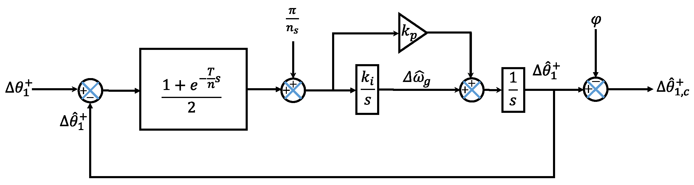
4. The Mathematical Model of the Proposed PLL

The proposed PLL’s mathematical model will be derived in this section to analyze the stability of the proposed PLL and derive a general design formula against the PI controller’s gains under any delay factor election. The mathematical derivation criteria in this paper follow the guideline of [23]. The extraction of the FFPS components in the dq-reference frame is utilized by applying Park’s transformation to the FFPS of the grid voltages as follows:
v d v q = 2 V m 3 sin θ ^ sin θ ^ 2 π 3 sin θ ^ + 2 π 3 cos θ ^ cos θ ^ 2 π 3 cos θ ^ + 2 π 3 sin θ ^ sin θ ^ 2 π 3 sin θ ^ + 2 π 3 ,
the FFPS of the grid voltage in the synchronous reference frame can be extracted using the trigonometric identities as follows:
v d = V m cos θ θ ^ ,
v q = V m sin θ θ ^ ,
The extracted fundamental components from the MDSC operator derived in Equations (25) and (26) are incorporated into the arctangent operation, which can be described as:
tan 1 v q t v d t = tan 1 v q t + v q t T n cos 2 π n s + v d t T n sin 2 π n s v d t + v d t T n cos 2 π n s v q t T n sin 2 π n s ,
Substituting Equations (25) and (26) into Equation (27) leads to the following:
tan 1 v q t v d t = tan 1 sin δ + sin γ cos 2 π n s + cos γ sin 2 π n s cos δ + cos γ cos 2 π n s sin γ sin 2 π n s ,
where:  δ = θ θ ^  and  γ = θ t T n θ ^ t T n .
Using trigonometric identities, Equation (28) can be simplified into:
tan 1 v q t v d t = tan 1 tan δ + γ + 2 π n s 2 ,
which can be written as:
tan 1 v q t v d t = θ θ ^ + θ t T n θ ^ t T n 2 + π n s ,
The arctangent function in Equation (30) extracts the phase error directly without any linearization procedure. Taking the Laplace transform of Equation (30) leads to the following:
M D S C s = 1 2 1 + e T n s Δ θ s Δ θ ^ s ,
The last equation represents the mathematical formula for the proposed PLL since it is valid under any selection of the delay factor  n , depicted in Figure 5. The term  π / n s , in Figure 5, represents the DC offset value in the output phase of the proposed PLL. It is equal to the estimated phase formula derived earlier in Equation (22), which justifies the proposed phase compensation model. Moreover, to derive a gain formula against the PI controller in terms of delay factor, it is tackled by taking the open-loop transfer function of the mathematical model of the proposed PLL as follows:
G o l = Δ θ ^ s Δ θ s Δ θ ^ s = V m 1 + e T n s 2 K P s + K i s 2 ,
the delay term in Equation (32) is approximated using Padé approximation to simplify the design process:
e T n s 1 T 2 n s 1 + T 2 n s ,
Substituting Equation (33) into the open-loop transfer function Equation (32) yields:
G o l = V m 1 T 2 n s + 1 K P s + K i s 2 ,
Applying the symmetrical optimum design method [24], the PI controller parameters are obtained as follows:
K P = 1 c T 2 n ,
K i = 1 c 3 T 2 n 2 ,
where c is a design constant that determines the phase margin (PM) of PLL, the PM of the PLL has the following formula:
P M = tan 1 c 2 1 2 c ,
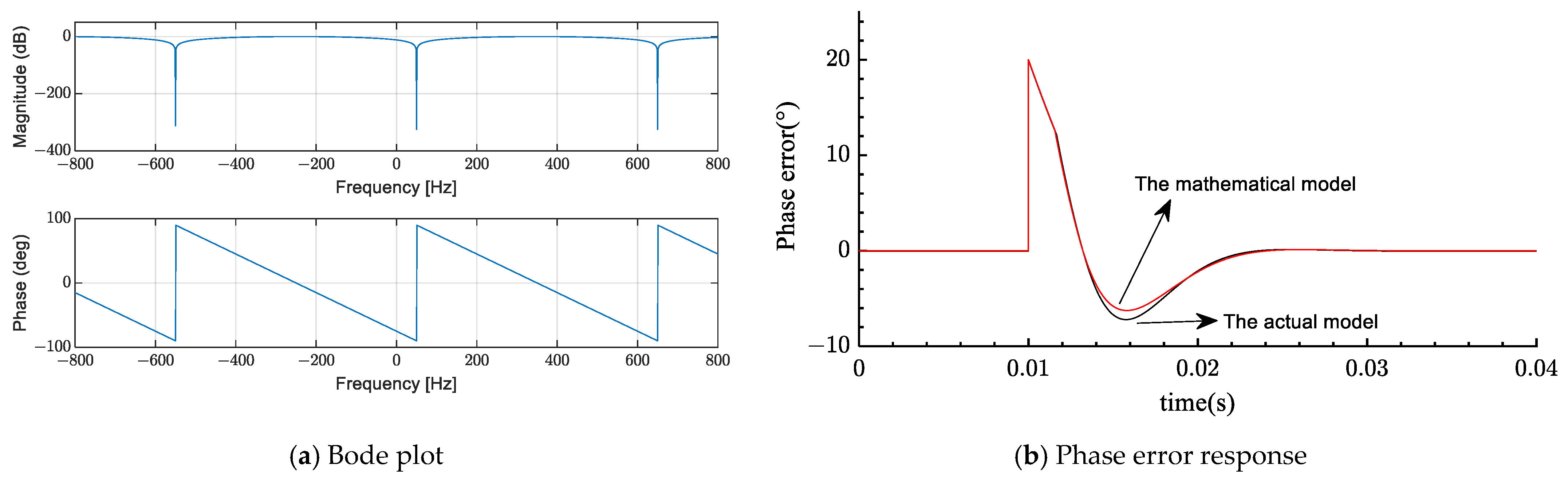
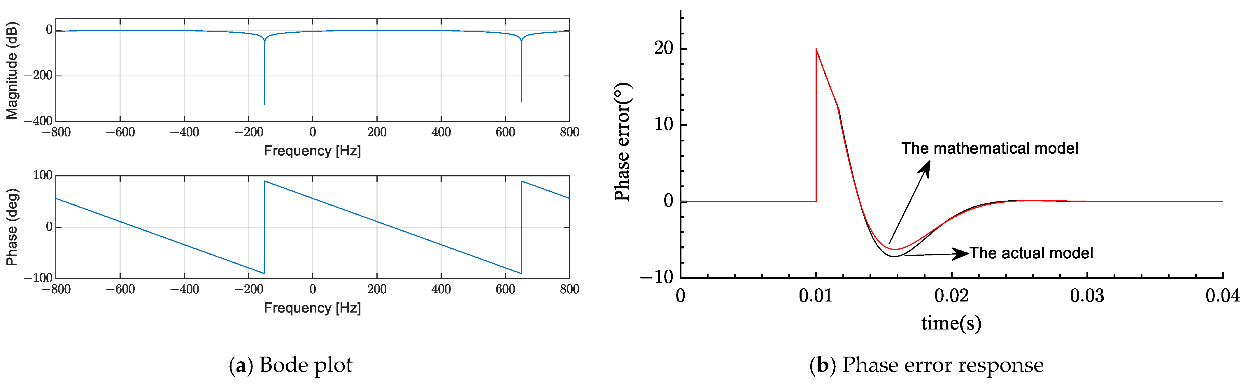
Equations (35) and (36) represent the formulas for the PI gains of the proposed model that corresponds to any selection of the delay factor  n , while Equation (37) corresponds to the desired phase margin of the system, which is taken here as in many approaches for fair comparison as  P M = 45 °  results in  c = 2 + 1 .

5. Numerical Simulations

5.1. The Validation of the Proposed PLL

Two delay factor values are selected and tested without generality loss to justify the proposed PLL capability in DC offset rejection while estimating the grid information under an arbitrary delay factor.

5.1.1. Case 1

The n =12, under this delay factor selection, the corresponding optimal value of  n s  can be obtained by substituting the delayed factor of  n  in Equation (17), which leads to  n s = 12 / 7 .
On the other hand, to compensate for the phase delay resulting from this selection, substituting the selected delay factor in the phase estimation formula derived in Equation (22) as follows:  φ l e a d = π 2 π 12 = 5 π 12  , so, the compensated value can be calculated as:  φ = 5 π / 12  and  k m = sin π 12  . The bode diagram of the MDSC against this case is plotted and depicted in Figure 6a. The BW of the operator, in this case, can be calculated using the relationship mentioned earlier, which results in (600 Hz) with a notch frequency located at (−50 Hz). The bode diagram shows that the magnitude of the MDSC operator with  n = 12  at 0 Hz is –11.7401 dB, which is equivalent to the same compensated value calculated mathematically. The estimated values against the phase and the BW are the same as the calculated values, which justifies the validation of the proposed model.
The general mathematical model derived earlier has been tested with the original model with a delay factor of  n = 12  for both models under a  + 20 °  phase jump in the grid voltage. Considering  c = 1 + 2  corresponded to  P M = 45 ° . The PI gains, in this case, are calculated from Equations (35) and (36) results in  K P = 497  and  K i = 102337.65 . The transient behavior of the phase error during the test for both models is depicted in Figure 6b. It can be observed that the mathematical model can estimate the dynamic behavior of the proposed PLL accurately.

5.1.2. Case 2

Under n = 16,  n s = 16 / 9  leads to:  k v = sin π 16  and  φ = 7 π / 16 . The Bode plot of the operator for this case is depicted in Figure 7a. It shows the same results obtained mathematically using the compensation formulas. Once again, the proposed model has been tested with its mathematical model with  n = 16  when the grid undergoes a  + 20 °  phase jump. The PI gains, in this case, are  K P = 662.74  and  K i = 181933 .  The simulated transient behavior of the phase error is depicted in Figure 7b, which justifies the accuracy of the mathematical model.

5.2. Comparisons with Related Methods

To validate its performance and applicability, the proposed PLL is compared with comparisons with the dqDSC2-PLL and NF-PLL, shown in Figure 8. The PI controller gains of the dqDSC2-PLL and the NF-PLL are the same as in [21]. Table 1 summarizes the control parameters of the PLLs under all test cases.

5.2.1. Test 1

The grid voltage is contaminated with the DC offset  v a , d c = 0.2 p u , v b , d c = 0.1 p u , v c , d c = 0.2 p u ,  meanwhile, the grid voltage undergoes a  + 20 °  phase jump. Figure 9 shows the simulation results for the phase error (Figure 9a) and the estimated frequency (Figure 9b) for all PLLs during this test. It can be observed that although all PLLs provide a good DC offset rejection capability under phase jump, the proposed PLL has the fastest transient response with a settling time of 12.18 ms. In contrast, the dqDSC2-PLL and NF-PLL have a settling time of 73.44 ms and 64 ms, respectively.

5.2.2. Test 2

The grid voltage is contaminated with the DC offset  v a d c = 0.2 p u , v b , d c = 0.1 p u , v c , d c = 0.2 p u , meanwhile, the grid voltage undergoes  + 5  Hz frequency step change. Figure 10 shows the simulation results for the phase error and the estimated frequency for all PLLs during this test, respectively. It can be observed that the NF-PLL cannot block the DC offset under this case, which causes an oscillation in the estimated frequency and the estimated phase angle. Simultaneously, the dqDSC2-PLL has a good DC offset rejection capability, but with a slow transient response of about 59.03 ms (2.96 grid cycles). On the other hand, the proposed -PLL shows an excellent rejection capability against the DC offset with precise and rapid frequency estimation, with a settling time of around 15.31 ms.

6. Experimental Validation

A three-phase inverter connected to a passive load through an LC filter is used to mimic a three-phase grid. Voltage sensors are used to sense the voltages and the compared PLLs are executed in parallel using a field programmable gate array (FPGA). For the proposed PLL, n is reduced to 4, which leads  K P = 165.68  and  K i = 11371 .  The control parameters for the other PLLs are the same as in Table 1, and the hardware setup rating is listed in Table 2, while Figure 11 shows its photos.
The results are captured using Rigol digital oscilloscope and are shown in Figure 12. Figure 12a shows the grid voltages under  + 25 °  while the DC offset is added at the same time to the phase voltages as  v a , d c = 0.2 p u , v b , d c = 0.1 p u , v c , d c = 0.2 p u . Figure 12b shows the estimated phase error, while Figure 12c shows the estimated grid frequency. Figure 12d shows the grid voltage under  + 6  frequency jump with DC offset, while its phase error response is shown in Figure 12e, and the frequency response is shown in Figure 12f. The experimental results show that the proposed PLL is at least three times faster than the other PLLs.

7. Conclusions

In this paper, the MDSC-PLL operating in dq reference frame is generalized for rejecting the DC offset contaminated with the grid voltage under any delay factor selection. The extension is based on a general mathematical relationship between a delay factor and a design parameter. It was shown that with the increase in the delay factor value, the dynamic response of the proposed PLL would increase at the cost of increasing the bandwidth. On the other hand, the proposed PLL was armed with compensation methods to estimate grid voltage amplitude and phase accurately to complete the grid parameters’ estimation. The compensation methods were derived based on general formulas and tested with the original model under an arbitrary delay factor. The proposed PLL is simulated under abnormal grid conditions and a comparative analysis is done with comparisons with other PLLs. Based on the results, the proposed PLL achieves grid synchronization in less than one grid cycle, making it at least two times faster than the other related PLLs. The results show that the proposed PLL has an excellent rejection capability against DC offset and accurate estimation for the grid parameters under any delay factor selection with a fast settling time.

Author Contributions

Conceptualization, I.A.S.; Software, A.A.I.; Validation, I.A.S., I.E.A. and A.A.I.; Investigation, A.A.I. and I.E.A.; Writing—Original Draft, A.A.I.; Writing—Review and Editing, I.A.S. and I.E.A.; Visualization, I.E.A.; Supervision, I.A.S. and I.E.A. All authors have read and agreed to the published version of the manuscript.

Funding

This research received no external funding.

Data Availability Statement

Not applicable.

Conflicts of Interest

The authors declare no conflict of interest.

References

  1. Xue, T.; Sun, P.; Xu, Z.; Luo, Q. Feedforward phase compensation method of LCL grid-connected inverter based on all-pass filter in weak grid. IET Power Electron. 2020, 13, 4407–4416. [Google Scholar] [CrossRef]
  2. Atawi, I.E.; Kassem, A.M.; Zaid, S.A. Modeling, management, and control of an autonomous wind/fuel cell micro-grid system. Processes 2019, 7, 85. [Google Scholar] [CrossRef] [Green Version]
  3. Smadi, I.A.; Kreashan, H.A.; Atawi, I.E. Enhancing the filtering capability and the dynamic performance of a third-order phase-locked loop under distorted grid conditions. Energies 2023, 16, 1472. [Google Scholar] [CrossRef]
  4. Atawi, I.E.; Al-Shetwi, A.Q.; Magableh, A.M.; Albalawi, O.H. Recent advances in hybrid energy storage system integrated renewable power generation: Configuration, control, applications, and future directions. Batteries 2023, 9, 29. [Google Scholar] [CrossRef]
  5. Gao, H.; Zhang, G.; Liu, X.; Wang, W. Study on six-phase PMSM control strategy based on improved position sensorless detection technology. IET Power Electron. 2021, 14, 1844–1855. [Google Scholar] [CrossRef]
  6. Chen, M.; Peng, L.; Wang, B.; Wu, W. Accurate and fast harmonic detection based on the generalized trigonometric function delayed signal cancellation. IEEE Access 2019, 7, 3438–3447. [Google Scholar] [CrossRef]
  7. Bamigbade, A.; Khadkikar, V.; Al Hosani, M.; Zeineldin, H.H.; El Moursi, M.S. Gain compensation approach for low-voltage ride-through and dynamic performance improvement of three-phase type-3 PLL. IET Power Electron. 2020, 13, 1613–1621. [Google Scholar] [CrossRef]
  8. Pranith, S.; Kumar, S.; Singh, B.; Bhatti, S.T. Improved gaussian filter based solar PV-BES microgrid with PLL based islanding detection and seamless transfer control. IEEE Trans. Ind. Electron. 2021, 69, 5815–5825. [Google Scholar] [CrossRef]
  9. Kulkarni, A.; John, V. Design of synchronous reference frame phase-locked loop with the presence of dc offsets in the input voltage. IET Power Electron. 2015, 8, 2435–2443. [Google Scholar] [CrossRef] [Green Version]
  10. Smadi, I.A.; Sultan, W. A phase-locked loop with an improved dynamic response under abnormal grid conditions. Comput. Electr. Eng. 2022, 97, 107645. [Google Scholar] [CrossRef]
  11. Smadi, I.A.; Fawaz, B.H.B. Phase-locked loop with DC-offset removal for single-phase grid-connected converters. Electr. Power Syst. Res. 2021, 194, 106980. [Google Scholar] [CrossRef]
  12. Ciobotaru, M.; Teodorescu, R.; Agelidis, V. Offset rejection for PLL based synchronization in grid-connected converters. In Proceedings of the 2008 Twenty-Third Annual IEEE Applied Power Electronics Conference and Exposition, Piscataway, NJ, USA, 24–28 February 2008. [Google Scholar]
  13. Smadi, I.A.; Issa, M.B. Phase locked loop with DC-offset removal for grid synchronization. In Proceedings of the IECON 2019—45th Annual Conference of the IEEE Industrial Electronics Society, Lisbon, Portugal, 14–17 December 2019; pp. 4669–4673. [Google Scholar] [CrossRef]
  14. Lubura, S.; Soja, M.; Lale, S.; Ikić, M. Single-phase phase locked loop with DC offset and noise rejection for photovoltaic inverters. IET Power Electron. 2014, 7, 2288–2299. [Google Scholar] [CrossRef]
  15. Wu, H.; Wang, X. Design-oriented transient stability analysis of PLL-synchronized voltage-source converters. IEEE Trans. Power Electron. 2020, 35, 3573–3589. [Google Scholar] [CrossRef] [Green Version]
  16. National Grid Electricity Transmission. The Grid Code: Revision 31; National Grid Electricity Transmission: Warwick, UK, 2008. [Google Scholar]
  17. Tsili, M.; Papathanassiou, S. A review of grid code technical requirements for wind farms. IET Renew. Power Gener. 2009, 3, 308–332. [Google Scholar] [CrossRef]
  18. Golestan, S.; Guerrero, J.M.; Vidal, A.; Yepes, A.G.; Doval-Gandoy, J. PLL with MAF-based prefiltering stage: Small-signal modeling and performance enhancement. IEEE Trans. Power Electron. 2016, 31, 4013–4019. [Google Scholar] [CrossRef] [Green Version]
  19. Lee, K.J.; Lee, J.P.; Shin, D.; Yoo, D.W.; Kim, H.J. A novel grid synchronization PLL method based on adaptive low-pass notch filter for grid-connected PCS. IEEE Trans. Ind. Electron. 2013, 61, 292–301. [Google Scholar] [CrossRef]
  20. Golestan, S.; Ramezani, M.; Guerrero, J.M.; Monfared, M. dq-frame cascaded delayed signal cancellation- based PLL: Analysis, design, and comparison with moving average filter-based PLL. IEEE Trans. Power Electron. 2015, 30, 1618–1632. [Google Scholar] [CrossRef] [Green Version]
  21. Golestan, S.; Guerrero, J.M.; Gharehpetian, G.B. Five approaches to deal with problem of DC offset in phase-locked loop algorithms: Design considerations and performance evaluations. IEEE Trans. Power Electron. 2016, 31, 648–661. [Google Scholar] [CrossRef] [Green Version]
  22. Li, Y.; Wang, D.; Ning, Y.; Hui, N. DC-offset elimination method for grid synchronization. Electron. Lett. 2017, 53, 335–337. [Google Scholar] [CrossRef]
  23. Li, T.; Li, Y.; Yang, J.; Ge, W.; Hu, B. A modified DSC-based grid synchronization method for a high renewable penetrated power system under distorted voltage conditions. Energies 2019, 12, 4040. [Google Scholar] [CrossRef] [Green Version]
  24. Hamed, H.A.; Abdou, A.F.; Bayoumi, E.; EL-Kholy, E.E. Effective design and implementation of GSS-PLL under voltage dip and phase interruption. IET Power Electron. 2018, 11, 1018–1028. [Google Scholar] [CrossRef]
Figure 1. Conventional SRF-PLL block diagram.
Energies 16 02873 g001
Figure 2. Time-domain implementation of the MDSC operator.
Energies 16 02873 g002
Figure 3. Schematic diagram of the MDSC-PLL.
Energies 16 02873 g003
Figure 4. Block diagram of the proposed PLL, where GMDSC is the generalized delayed signal cancellation block.
Energies 16 02873 g004
Figure 5. Mathematical model of proposed PLL.
Energies 16 02873 g005
Figure 6. (a) Bode plot of the MDSC operator with n = 12. (b) Accuracy assessment of the mathematical model of the proposed PLL with n = 12.
Energies 16 02873 g006
Figure 7. (a) Bode plot of the MDSC operator with n = 16.; (b) Accuracy assessment of the mathematical model of the proposed PLL with n = 16.
Energies 16 02873 g007
Figure 8. Block diagrams of the (a) dqDSC2-PLL, (b) NF-PLL.
Energies 16 02873 g008
Figure 9. Comparisons between related PLLs under test1 condition: (a) the estimated phase error; and (b) the estimated frequency.
Energies 16 02873 g009
Figure 10. Comparisons between related PLLs under test 2 condition: (a) the estimated phase error; and (b) the estimated frequency.
Energies 16 02873 g010
Figure 11. The hardware setup photo.
Energies 16 02873 g011
Figure 12. Comparisons between related PLLs.
Energies 16 02873 g012
Table 1. The controller parameters.
ParametersdqDSC-PLLNF-PLLProposed-PLL
  Delay   factor   n 2-8
  Proportional   gain   k P 82.8492331.37
  Integral   gain   k i 2842.73507.145483
Table 2. The controller parameters.
ParametersValue
Rated Power200 watt
Input DC voltage 64 V
Grid frequency50 Hz
Rated phase current4 A
Filter inductance 1.5 mH
Filter capacitance2 μF
Switching frequency 10 kHz
Disclaimer/Publisher’s Note: The statements, opinions and data contained in all publications are solely those of the individual author(s) and contributor(s) and not of MDPI and/or the editor(s). MDPI and/or the editor(s) disclaim responsibility for any injury to people or property resulting from any ideas, methods, instructions or products referred to in the content.

