1. Introduction
The miniaturization of device packages, together with the creation of components capable of working at ever higher frequencies and dissipating greater power, has led to an increase in heat flow in systems [
1]. One of the biggest difficulties has always been removing the heat generated by the device to meet its thermal requirements while ensuring optimal performance [
2]. Thermal management is one of the strategic areas of research and development for electronics manufacturers worldwide [
3]. Sophisticated heat sink designs have been developed, new materials for heat transfer have been discovered, and complex cooling systems have been designed [
4,
5] in order to keep the junction temperature of the semiconductor device below the maximum permissible limit.
When an electronic device is subject to heating/cooling cycles, the mechanical stress associated with the thermal expansion of its different materials may cause the detachment of silicon from the metal case or even micro-cracks in the semiconductor [
6]. These thermal stresses can cause a reduction in the device’s usable lifetime and reliability issues [
7]. In this respect, the estimation of the device’s peak temperature for a current through the device would enable the evaluation of the thermal resistance, Rth [
8].
The estimation of the thermal resistance is fundamental when designing the device packaging [
9]. To this end, a thermal simulation is required for efficient thermal management as it enables the evaluation of the effect of different dissipating elements, and their placement, on the chip. In [
10], mechanical-thermal co-design has been used for the optimization of the electronic package module. A method for thermal characterization of GaN-based transistors using coupled simulation has been proposed in [
11]. CAD technology has been used for modelling the power distribution profiles while finite element analysis has been adopted for simulating the global thermal behavior; the results were combined to improve the model accuracy. 3-D thermal simulations have been used in [
12], in order to evaluate the variation of the thermal resistance of GaN High Electron Mobility Transistors (HEMTs) at varying gate geometries. The information is useful when producing suitable circuit models at the design stage. Similarly, ref. [
13] has proposed a methodology for extracting the thermal equivalent circuit of a high-density GaN-based power stage using a synchronous buck converter as the test vehicle.
The relation between the breakdown of advanced GaN structures and thermal resistance has been investigated in [
14]. Transient thermometry techniques have been used for localizing heating sources using nanoscale thermal transport analysis [
8]. A transient electrical characterization method used to determine the temperature in a transient self-heating state of GaN HEMTs has been proposed in [
15], which also experimentally identified the heat source. Despite the aforesaid efforts and innovative solutions, thermal characterization of GaN HEMT devices is still in its early stage [
16,
17,
18].
This paper analyzes the primary benefits and limitations of using temperature-sensitive electrical parameters (TSEPs) for thermal resistance characterization. TSEPs use passive probes to measure electrical quantities at the device terminals without direct access, and these quantities are adopted to estimate the junction temperature, Tj [
19]. This approach has limited intrusiveness at the device level [
20], making the use of TSEPs an interesting approach [
21]. In particular, the on-state drain-source voltage, gate-source voltage, and gate current have been experimentally analyzed as they are measurable quantities, considering the device characteristics.
The remainder of this paper is organized as follows.
Section 2 shows some solutions for the estimation of the junction temperature and the characterization of the thermal resistance. A description of the TSEP calibration procedures and some results are reported in
Section 3, where the main advantages, limits, and best application fields of the different TSEP are reported. Finally, the conclusions are presented in
Section 4.
2. Estimation of the Junction Temperature and Thermal Resistance Characterization
This section first describes the main techniques adopted for junction temperature estimation, primarily focusing on TSEPs. Then, the adoption of TSEPs for evaluating the thermal resistance of GaN HEMTs is analyzed.
Optical methods exploit the dependence between temperature and photoemission [
22]. In this field, the use of an integrated photodiode or infrared camera enables contactless temperature monitoring [
23]. The use of special paints to print the surface increases the accuracy but also increases the costs [
24]. The adoption of optical fibre enables high resolution and fast response time, but it is an expensive solution.
Physical methods execute Tj measurement by contacting thermo-sensitive materials with the device surface [
25]. Various pieces of equipment have been used for the measurement: thermocouples, thermistors, scanning thermal probes, multiple contact or blanket coatings, etc. The time response of the probe is the primary limitation when tracking thermal variations. The need for contact is another limit that makes it useless in high-voltage applications.
Electrical methods use some proprieties of the semiconductors that depend on the temperature [
26]. Thermal test chips, e.g., resistance temperature detector or diode, are fabricated on the device surface. In the first case, the temperature sensor is a thermistor whose voltage drop changes as its resistance changes due to a temperature variation. In the second case, the modification of the forward voltage is adopted for detecting a temperature variation. The significant cost and layout modification complexity are their primary drawbacks. For this reason, the TSEP are the most used electrical methods thanks to their ability at indirectly inferring the temperature by measuring the current flowing through the device or the voltage drop across it. In this case, the electrical quantities are measured at the device terminals employing simple op-amp-based electronic circuits, thereby avoiding intrusive direct access. The quantities used for Tj estimation are: on-state voltage [
27]; threshold voltage [
28]; saturation current [
29]; Miller plateau [
30]; switching time delay [
31]; peak gate current [
32,
33]; and current and voltage switching speed [
34].
Generally, TSEPs are widely used for device condition monitoring [
35] because they combine good accuracy with a strong ability in tracking fast temperature transients [
36]; however, the granularity in the case of multi-die is limited. In the last few years, some studies have adopted TSEPs to determine the thermal resistance of GaN HEMTs.
In [
37], the use of the forward voltage (i.e., a TSEP) of an AlGaN/GaN Schottky junction has been able to obtain good linearity and the results have shown good accuracy. However, this approach cannot be used online, i.e., the measurements cannot be performed during the normal functioning of the device but only after it is shut down. Consequently, the channel temperature reduces in the interval between when the device is turned off and the acquisition of the TSEP is performed: the longer the delay time, the lower the tested temperature. Moreover, this method is complex.
The conduction resistance and the forward voltage drop between the gate and source are TSEPs that have been proposed to test the thermal characteristics of the GaN HEMTs [
38]. However, few details have been provided on the evaluation of thermal resistance using these quantities. Furthermore, sensing the conduction resistance is problematic because the overall conduction resistance is the sum of the junction resistances and the bond wires and solder joints [
39]. An interesting approach based on using the gate current or the drain-source voltage as a TSEP is reported in [
21]. The current sensing is indirectly obtained through a resistor, which is also used to avoid electric stresses during the turn-on. The results are accurate and reproducible, but the access to the measurement is complex.
3. Considered TSEP for Thermal Resistance Characterization in GaN HEMTs
The temperature characterization has been performed using the following TSEPs:
- ➢
Vds (on-state drain-source voltage)
- ➢
Vgs (gate-source voltage)
- ➢
Ig (gate current)
They have been selected because of their good features, including linearity, calibration process simplicity, accuracy, and the possibility of online temperature measurements.
Linearity is an interesting indicator for data processing. It is also important for the calibration step because a linear TSEP does not need a lot of measurement points. The calibration of a TSEP is an important step in the temperature assessment of the device. In particular, the relationship between the TSEP and device temperature is determined by a calibration procedure that consists of a measurement of the TSEP at different values of temperature [
19]. Every TSEP requires a calibration step, and the calibration time depends on the TSEP. For GaN devices, the calibration curve can significantly change from one GaN HEMTs device to another in the same product family, but it does not influence the final calculation of Rth.
First, an estimation of the thermal impedance, Zth, is performed considering the Tj evaluation at 120 s. Then, the steady-state Tj is estimated in order to perform the Rth calculation. Finally, a simple relation between them, that enables the smaller Zth estimation time to benefit, is reported. For each TSEP and testing current, 10 measurements have been performed and the average value of Zth and Rth have been evaluated; the difference between the average value and the extrema (minimum and maximum) has also been noted.
For all three TSEPs (
Vds,
Vgs, and
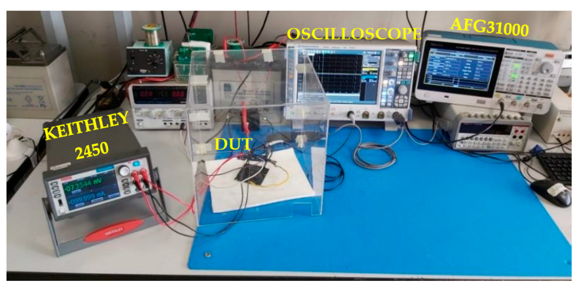
Ig), the equipment used for the calibration and measurement is shown in
Figure 1 and
Figure 2. The calibration process has been carried out using the following tools:
The equipment includes:
- -
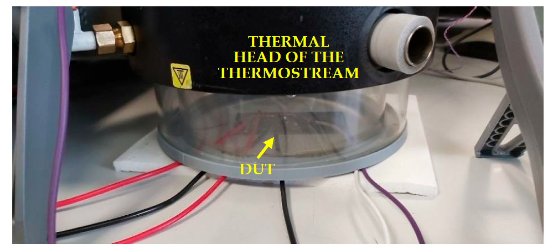
a thermostream, to force the device under test (DUT) at different temperatures;
- -
a source meter 2450;
- -
a thermocouple to monitor the temperature.
To perform the Rth measure, a test bench has been equipped with a Digital Oscilloscope RTO 2014 to view the waveforms of TSEPs used (Vds, Vgs, and Ig). The GPS-3303 Power Supply is exploited to supply the gate of the DUT, while 6060B is used as an active load, which is driven by an AFG31000 Arbitrary Function Generator. A Source Meter 2450, set in the 4-wire mode, is used to force a current and simultaneously read the variations of the TSEPs (Vds, Vgs, and Ig), and a thermocouple is used to monitor the temperature.
It is worth noting that the Zth and Rth evaluation (e.g., Equation (3)) requires the concurrent knowledge of the junction temperature increment (ΔTj) and the incoming power that has caused it. However, there is no accurate and simple way to concurrently measure these quantities while the GaN HEMT is working. An indirect measurement of Tj is necessary and the TSEPs are adopted to fulfil this purpose. From this perspective, it is necessary to know the value of the TSEP at different Tj (for example see the calibration curves in
Section 3.1)
The calibration process aims to obtain this information to find a mathematical relationship between the TSEP and Tj (e.g., Equation (1)). At this stage, it is necessary to determine the junction temperature for each measured value of the TSEP. Therefore, the ambient temperature is set at different values using the thermostream heater and a small test current is applied to perform the TSEP measurement. The junction temperature is assumed to be equal to the ambient temperature at this stage. This condition is true if the self-heating due to the test current is negligible.
During the Zth or Rth evaluation, the initial Tj is equal to the room temperature; it is increased by a large pulsed current (i.e., it causes self-heating expressly to increase Tj). The power generated into the device is estimated from the known heating current and the measured drain-source voltage. At this stage, the information acquired during the calibration process is used to estimate Tj from the TSEP measurement. In detail, the mathematical relation (e.g., Equation (1)) is rearranged to evaluate Tj according to the TSEP (e.g., Equation (2)).
Finally, it is worth noting that the value of these TSEPs changes over time; consequently a TSEP measure at an early stage and after a significant amount of time provides different values under the same Tj. Therefore, the calibration performed at an early stage to evaluate the Rth cannot be used accurately after an extended time. In this case, it is necessary to repeat the calibration process to account for the effect of device degradation on the TSEPs.
The Zth and Rth measurements have been performed on a GaN power transistor device soldered on a 2-layer application board with the following characteristics:
- ➢
- ➢
- ➢
- ➢
Package: PowerFLAT 5 × 6 HV
3.1. On-State Drain-Source Voltage TSEP
The first TSEP used is on-state drain-source voltage,
Vds. The relationship between the TSEP and the temperature has been first determined by employing a calibration process. The setup used to perform this initial step is shown in
Figure 3.
During the calibration, the source meter 2450, set in the 4-wire mode, forces a 100 mA current while simultaneously measuring the variations of the Vds. A very important aspect to emphasize is that, for the calibration to be carried out correctly, it is necessary to apply a current that avoids the DUT self-heating. In addition, the calibration has been performed starting at the ambient temperature and then increased to 80 °C.
The device has been placed in a glass chamber (
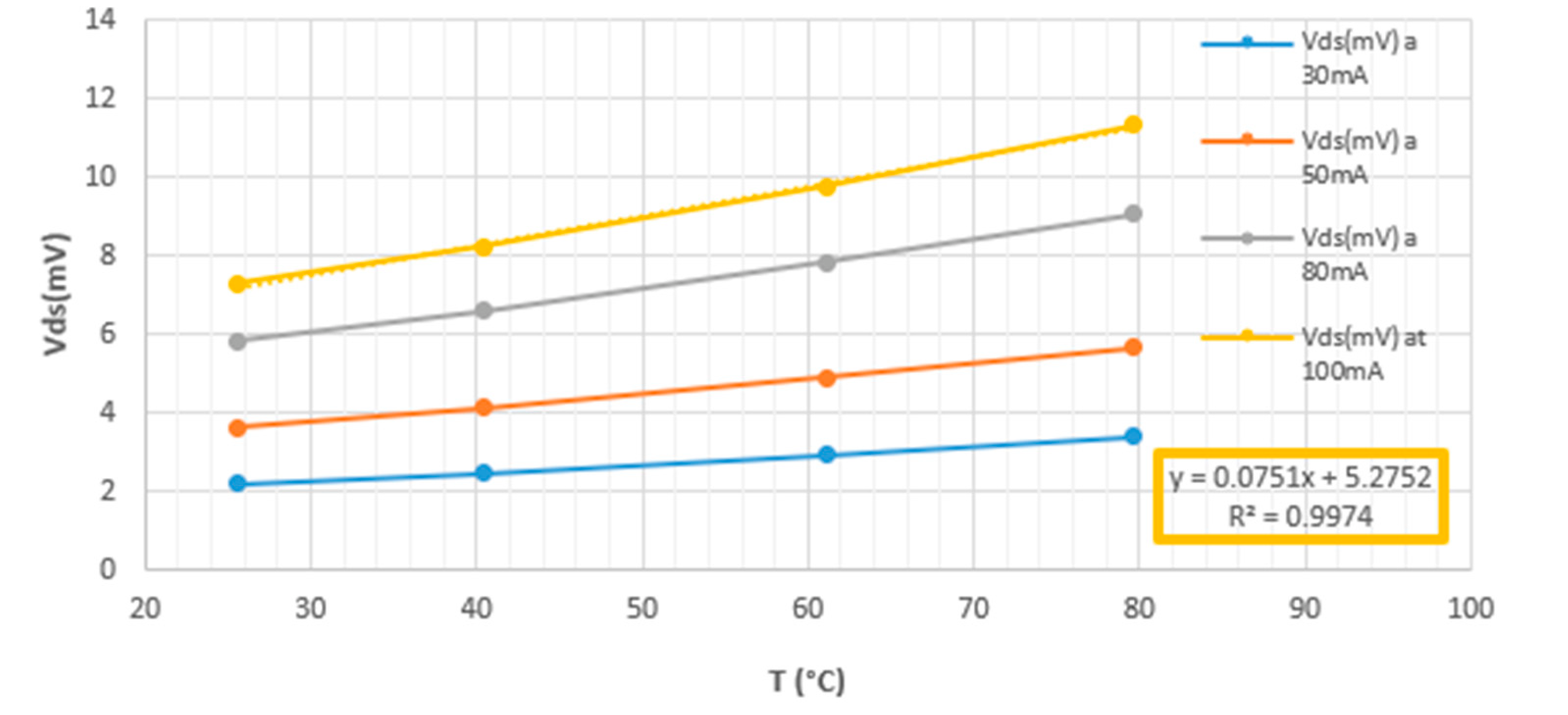
Figure 4) so that the airflow from the thermostream heats the DUT. The calibration curves of the
Vds vs. the temperature carried out using four sensing currents are shown in
Figure 5.
As expected, the value of the
Vds increases as the temperature increases. During the calibration phases, four different current values were used: 30 mA, 50 mA, 80 mA, and 100 mA. In addition,
Figure 5 shows that the trend of the
Vds with the temperature was almost linear and the factor
was about 0.9974 for any current.
Considering the curve at 100 mA, which is the best compromise between accuracy and avoiding self-heating, the following expression is obtained:
In this equation, the ambient temperature (set by the thermostream) and the junction temperature coincide because a test current that avoids the self-heating has been used. Therefore, a simple relation between Tj and the drain-source voltage can be derived from Equation (1):
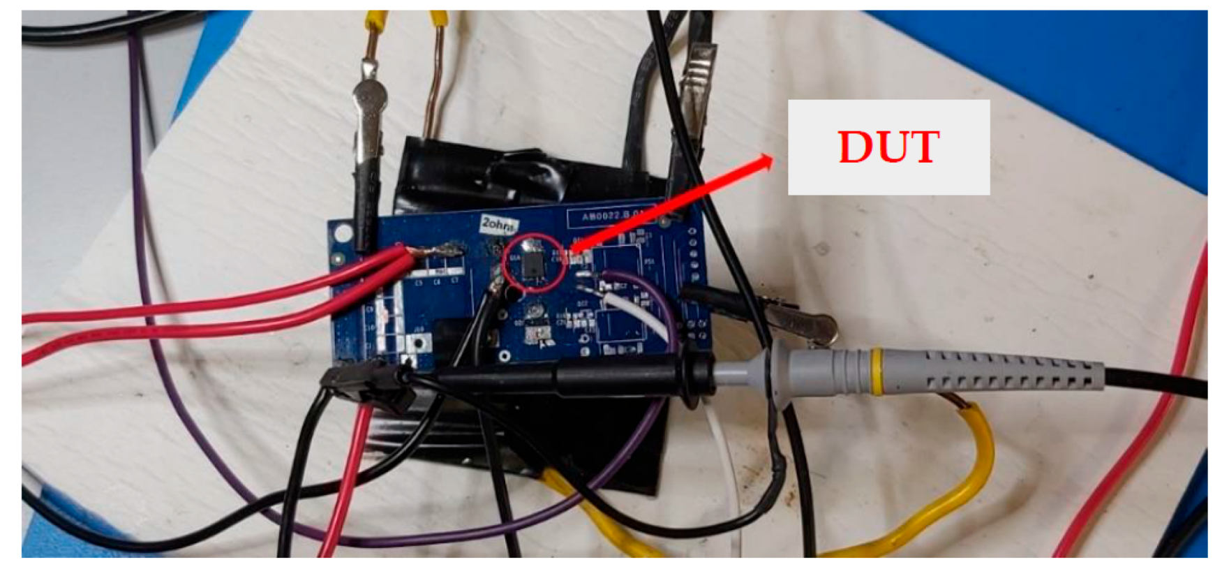
To carry out the thermal characterization of the device, the test conditions reported in
Table 1 and the setup reported in
Figure 6 and
Figure 7 have been used. Equation (2) is valid when Tj is in the calibration range. The current values refer to Ids.
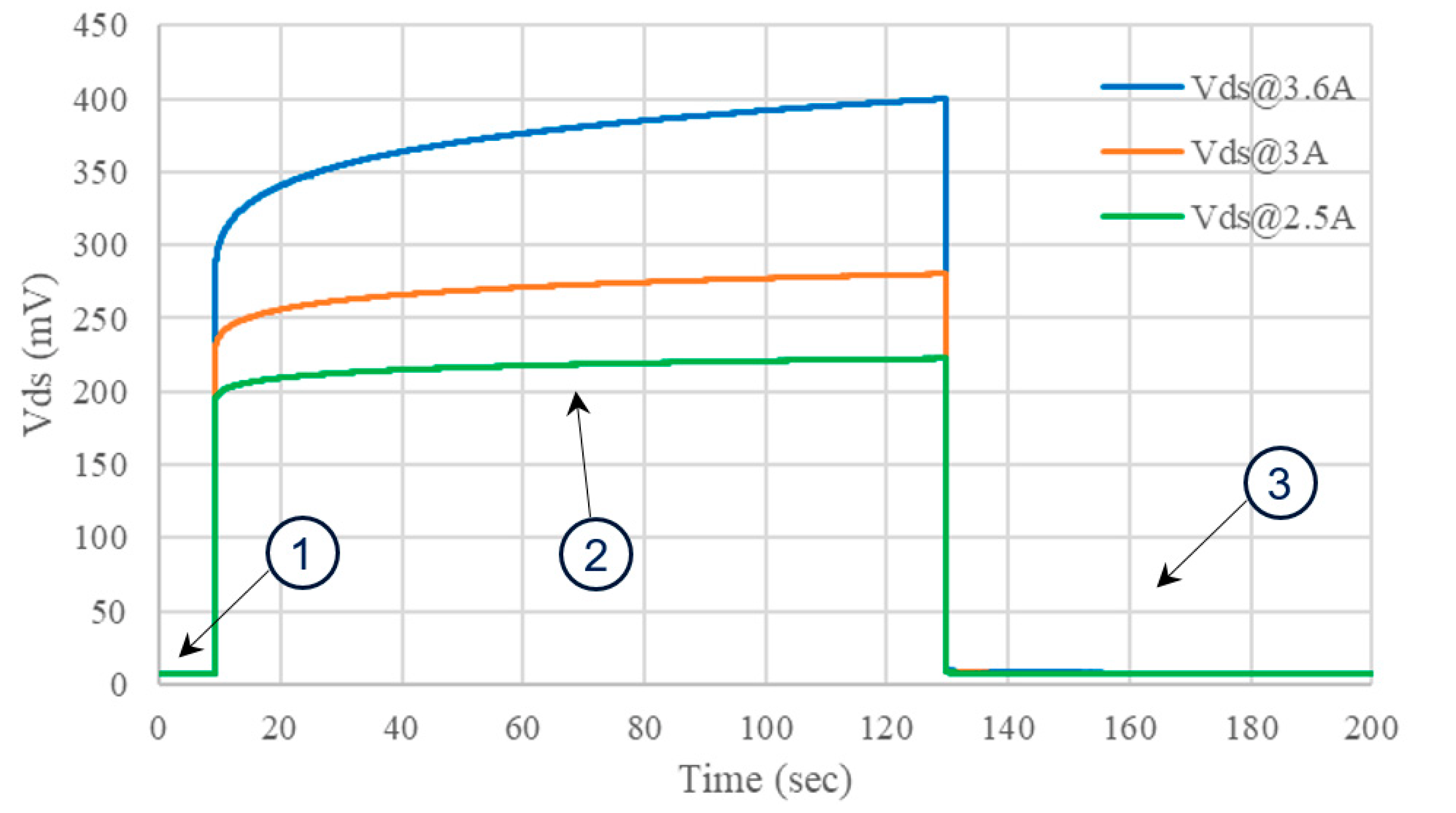
During the measurement, three different heating currents were used (2.5 A, 3 A, and 3.6 A). For each of them, 10 measurements were performed to ascertain the robustness of the method. Some of these measurements are reported in
Figure 8 where, during the interval labelled “1”, the device was at room temperature with no heating current, so the value of
Vds was measured for a current equal to 100 mA.
Once the heating current pulse is applied (“2”),
Vds instantaneously increased significantly due to the large current. Then, the device began to heat up and, consequently,
Vds increased further. When the pulse vanished (“3”), the heating current no longer flowed into the device and only the sensing current flow remained. Consequently, the cooling phase began, and, in the end,
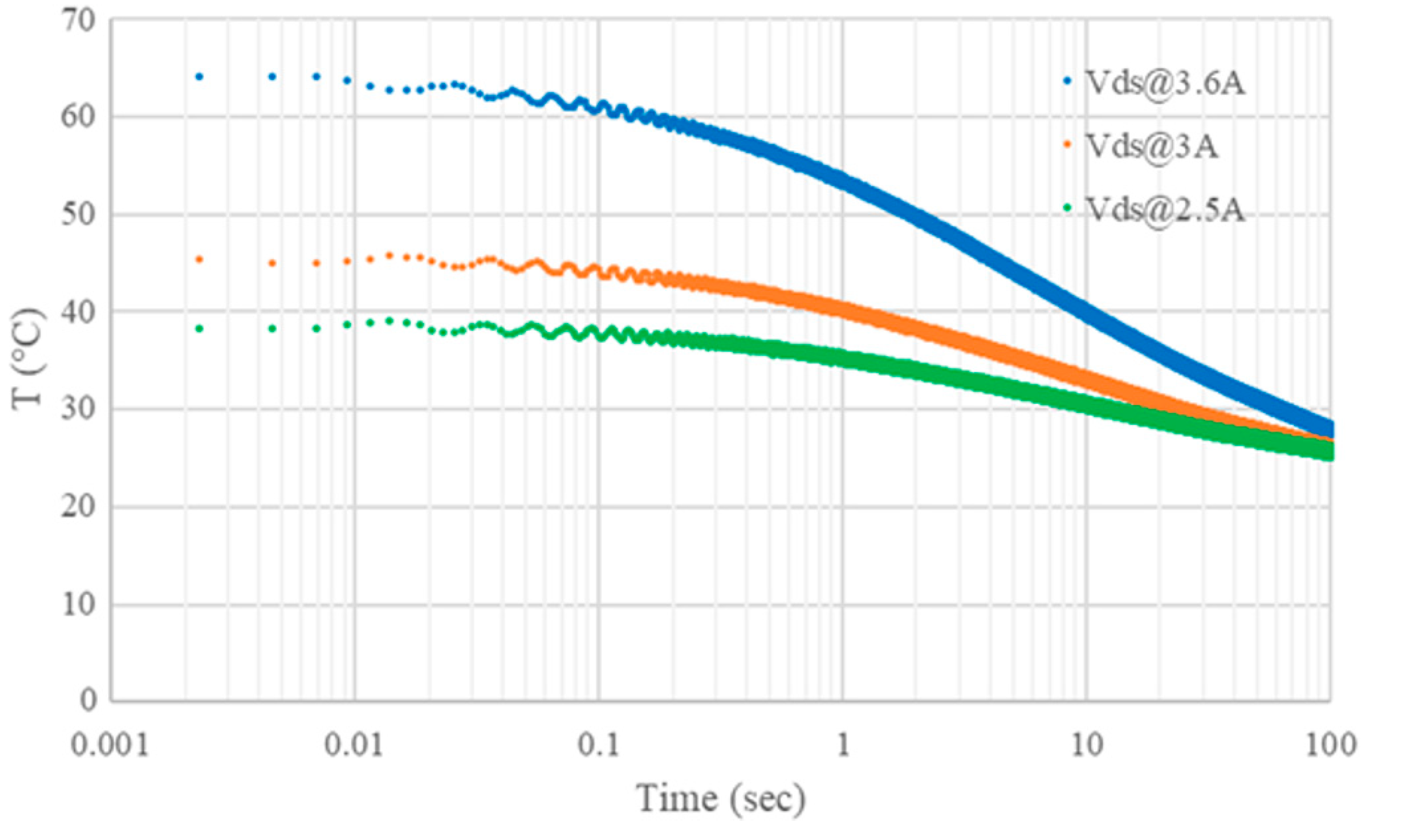
Vds returned to the initial value. The cooling curves of the
Vds have been reported in
Figure 9. As mentioned before, during the interval “1”,
Vds is measured using Equation (2) to indirectly measure the initial Tj (
). Similarly, at the beginning (after 100μs) of interval “3”,
Vds is measured again to indirectly estimate the new Tj (
).
Indicating with:
the average value of Vds during the interval “2”;
the temperature before the application of the heating current, , i.e., at t = 0 s; the value of the temperature when is removed and only the sensing current flows into the DUT;
then, the thermal impedance (i.e., at
@120s) or the thermal resistance (i.e., at
@1000s) can be computed as follows:
where
,
.
Equation (3) is valid when Tj is in the calibration range. The Zth calculation can be performed using Equation (3) when Tj is in the calibration range. The difference with the Rth calculation is the choice of
; it is equal to the steady-state temperature for Rth evaluation, but it is lower for Zth evaluation. During the calibration process, and at the beginning of the Zth or Rth evaluation (
), the junction temperature is equal to the ambient temperature. After that, they differ once the pulsed current is adopted (
).
Table 2 reports the average value of Zth evaluated according to Equation (3) by considering the three heating currents. For each current, the difference between the average value of Zth and the minimum and maximum values obtained during the ten tests is lower than 2%.
Linearity is an advantage of this approach., In contrast to the approaches based on the other two TSEPs, it does not need an accessible gate pin.
The challenge is the detection of small voltage variations. The sensing current must be increased to increase the voltage variations, thus facilitating appreciation of the voltage variations. On the other hand, the self-heating could become not negligible if the sensing current is too high. In this work, a current value of 100 mA is the best compromise to limit the self-heating current while maintaining a good accuracy in Vds voltage measurement.
The use of Vds as a TSEP for Rth estimation should be avoided when the device presents a conduction resistance value below 10 mΩ. In fact, it is difficult to understanding if a small Vds variation (μV) is due to the variation of the conduction resistance or to the variation of the parasitic resistance of metallic contacts (leads, bonding wires, and so on). As such, thermal resistance characterization using Vds is preferable when the parasitic resistances are negligible.
3.2. Gate-Source Voltage TSEP
In this case, the first step was calibration to determine the relationship between
Vgs and temperature. The setup used to perform this initial step is shown in
Figure 10.
The calibration was performed by measuring the
Vgs at a sensing current of 45 uA forced by the source meter. The value of the current was appropriately chosen to ensure that, during the calibration step, the
Vgs was in a range that enabled the device to turn on. The calibration curve of
Vgs vs. temperature is reported in
Figure 11.
The gate-source voltage can be expressed as a function of the imposed temperatures once the calibration process has been performed:
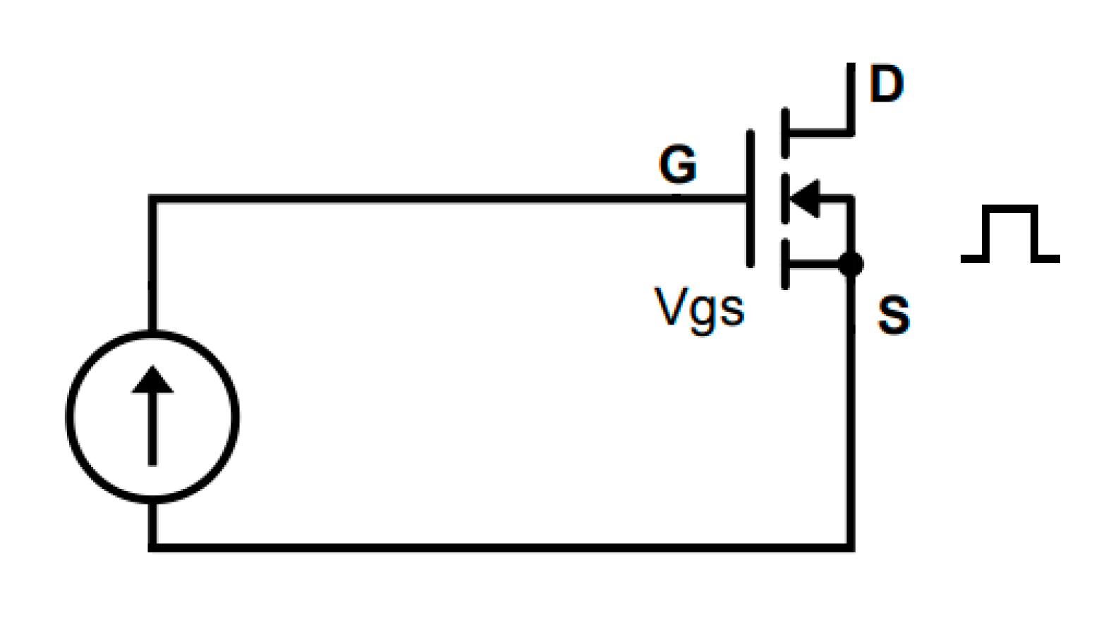
In order to carry out the thermal characterization of the device, the test conditions reported in
Table 3 were considered, and the setup is indicated in
Figure 12. The heating current values refer to Ids while the sensing current refers to
Ig.
The results of the measurement are shown in
Figure 13.
Looking at
Figure 13, in the first part (labelled “1”), the device was operating at room temperature, similarly to the previous TSEP, so the value of
Vgs was measured and T
j,0 is indirectly estimated when only the sensing current was applied. Once the heating current was applied (“2”), the device began to heat up. When the current pulse was interrupted (“3”), the heating current no longer flowed through the device and
Vgs was measured (after 100 μs due to the pulse interruption) to obtain Tj
end. After that, the cooling phase began and
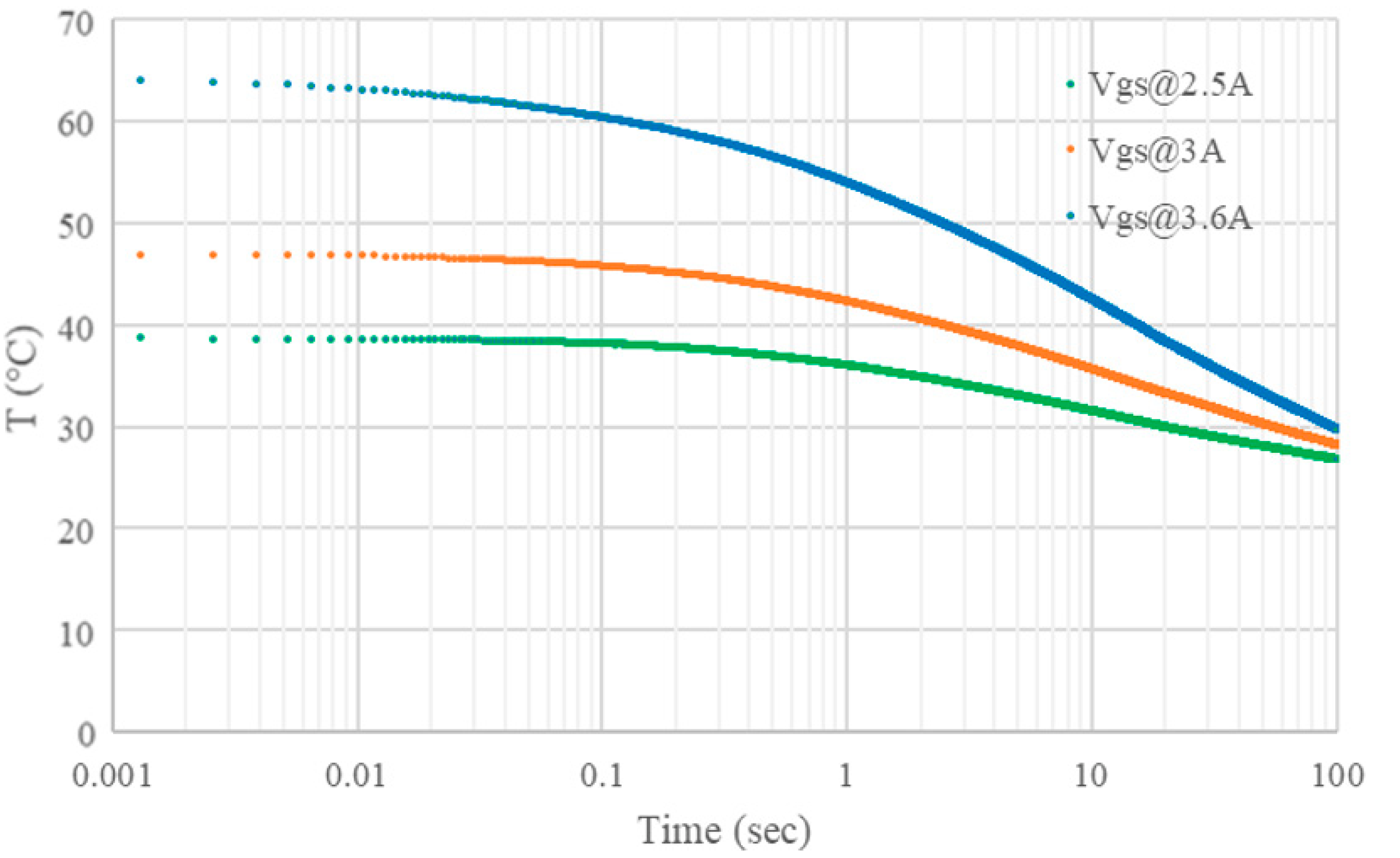
Vgs started increasing, thus returning to the initial value. The cooling curves of
Vgs are reported in
Figure 14 for different heating currents.
Analyzing the cooling curve, it is evident that, when the pulse is removed, the value of
Vgs begins to decrease until it reaches room temperature. As aforementioned, as for the previous TSEP, Tj (thus Tj
0 and Tj
end) is derived from the Equation (4), as:
Equation (5) is valid when Tj is in the calibration range.
Table 4 reports the average values of Zth computed using Equations (3) and (5) as a function of the heating currents applied. In this case, the difference between the average and extrema is lower than 2%.
The primary advantage of this approach is related to the measurement instrumentation used because it is not particularly critical in terms of performance and accuracy. In fact, the gate-source voltage presents a volt order of magnitude that enables the measurement to be obtained with high precision. The gate current value (typically μA is the order of magnitude) must be properly chosen to avoid the device being accidentally turned off due to the temperature increment.
On the other hand, this approach cannot be used when the gate pin is not available. This case occurs when GaN devices using system-in-package (SIP) solutions are considered because they have a driver circuit integrated and the gate pin is not connected to any outside pin. When the pin is available, Vgs TSEP is more suitable than Vds for devices with low conduction resistance. The lack of linearity is an additional (minor) drawback of the method.
3.3. Gate Current TSEP
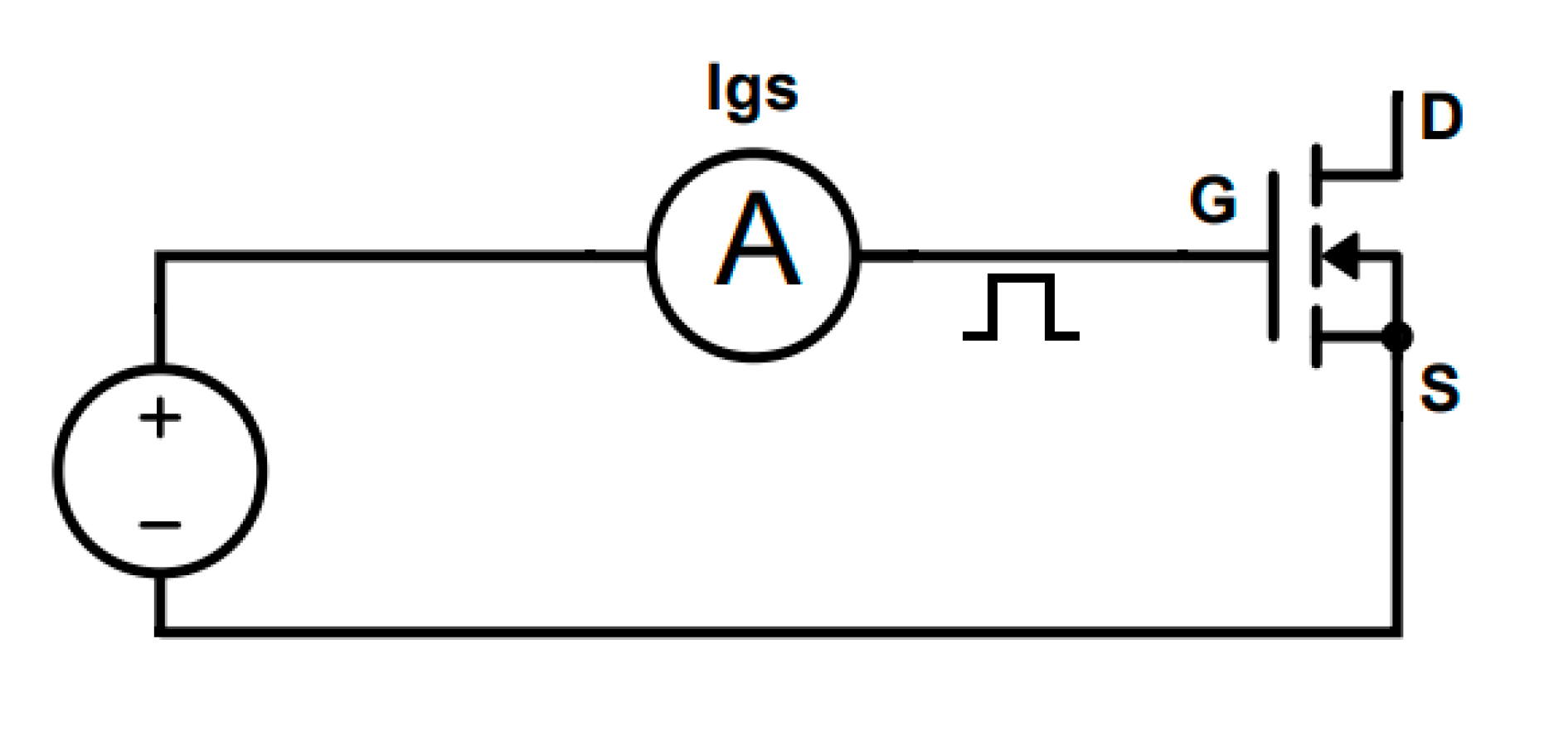
The setup used to perform the calibration is shown in
Figure 15. The calibration was performed by measuring
Ig at a sensing voltage of 6 V. The value of the voltage was chosen according to the datasheet threshold voltage. The calibration curve of
Ig vs. temperature is shown in
Figure 16.
Once the calibration process was performed, the interpolation function was obtained:
The test conditions are reported in
Table 5 and the setup of
Figure 17 has been adopted in order to carry out the thermal characterization of the device.
The result of some measurements is shown in
Figure 18.
Figure 18 shows, in the first part, the device gate current at room temperature (the value of
Ig at 6 V). As for the previous TSEP, the value of
Ig is used for Tj
0 evaluation. Following the application of the pulse, shown in part 2, the device began to heat up. When the pulse was interrupted, in part 3, the heating current no longer flowed through the device. When the pulse was removed,
Ig was measured, after 100 μs, for T
j,end evaluation. Then, the cooling phase began and
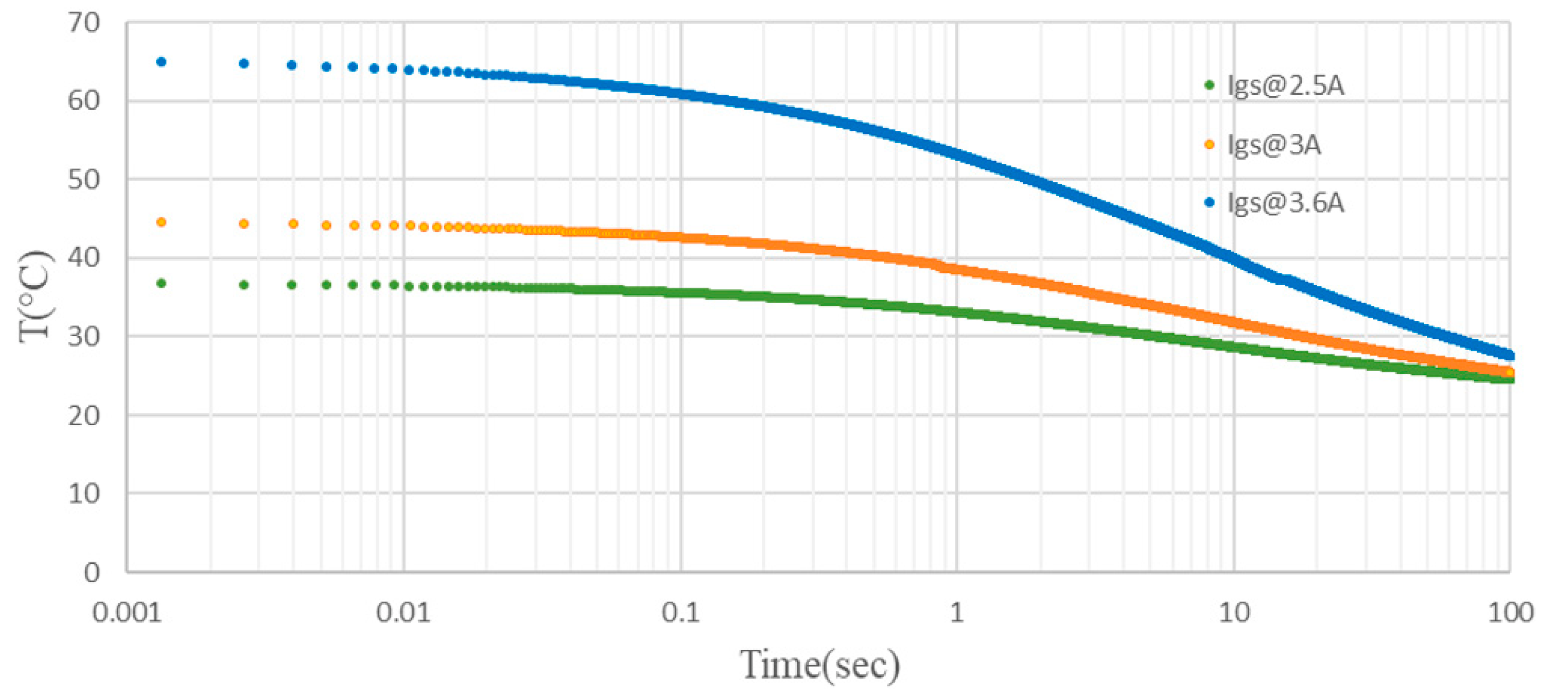
Ig started decreasing and returned to the value presented before the application of the pulse. Some cooling curves of
Ig are reported in
Figure 19.
Analyzing the cooling curves, it is evident that when the pulse is removed the value of the gate current begins to decrease and, in the end, reaches room temperature. The value of Tj can be derived and, consequently, the evaluation of T
j,0 and T
j,end is obtained by rewriting Equation (6) as:
Equation (6) is valid when Tj is in the calibration range.
Table 6 reports the average values of the thermal resistance computed using Equations (3) and (7), as a function of the three heating currents applied. In this case, the difference between the average value and the extremes is lower than 2% for each current level.
The use of Ig as a TSEP for evaluating the thermal resistance presents almost the same advantages and limits reported for the Vgs. The accurate setting of Vgs ensures the optimal conditions for the Ig measurement while the device is in on state. However, Vgs is preferable to Ig as a TSEP because expensive sensing circuitry is necessary for current measurement due to its low value (μA). In this application, to make the measurement robust to the noise, the Printed Circuit Board has been designed to place the sensing pin close to the DUT. The gate current measurements have been performed using a Keithley 2450 that presents a 5 μA resolution, while the DUT gate current order of magnitude is tens or hundreds μA.
In summary, regardless of the TSEP and current level, the difference between the average and minimum or maximum value is always less than 2%. The measurements carried out also show that the three TSEPs (
Vds,
Vgs, and
Ig) have a similar temperature trend and that the average Zth presents a limited variation for a given current value. For example, it is about 1% when a 3.6 A heating current is considered, as shown in
Table 7. The table also reports the value of Rth obtained as the average value among ten measurement repetitions for each TSEP. Differently from Zth, the maximum difference between the average value and the extremes (minimum and maximum Rth for the given TSEP) is less than 1%. Another difference between Zth and Rth is their dependence on the pulsed heating current. Zth increases as the current decreases while no appreciable difference among the Rth values occurs at the three currents. Equation (3) is useful to understand the reasons behind this different behavior. First, it is worth noting that when Rth is computed using Equation (3), Tj has reached the steady-state value (the maximum value) and then the value of Rth is greater than the value of Zth, which is computed while Tj is increasing. At a low current, the steady-state temperature is reached after a shorter time, thus the Tj evaluated at 120 s is closer to the one measured at 1000 s than it is in the case of a large current that involves greater temperature variation. Consequently, the value of Zth at a low current is greater than the value at a higher current. However, since the Zth evaluation also depends on the average
Vds, and this quantity arises during the heating period when Zth is evaluated, the value of P in Equation (3) is less than the one used for Rth, thus reducing the difference among the Zth value evaluated at the three different currents.
Finally, as can be seen in
Table 7, Zth enables a good estimation of Rth, since the former is about 80% of the latter, thus leading to timesaving (1200 s vs. 10,000 s).
Figure 20 shows the comparison between the cooling curves of the 3 TSEPs at the same heating current:

