Abstract
Monitoring the temperature of a semiconductor component allows for the prediction of potential failures, optimization of the selected cooling system, and extension of the useful life of the semiconductor component. There are many methods of measuring the crystal temperature of the semiconductor element referred to as a die. The resolution and accuracy of the measurements depend on the chosen method. This paper describes known methods for measuring and imaging the temperature distribution on the die surface of a semiconductor device. Relationships are also described that allow one to determine the die temperature on the basis of the case temperature. Current trends and directions of development for die temperature measurement methods are indicated.
1. Introduction
Semiconductor elements are used to construct devices used in many industries. The solutions used in electromobility [1], renewable energy [2], health protection [3] and Internet of Things (IoT) [4] are the fastest developed. Devices that work as IoT nodes can be used in applications related to Industry 4.0 [5].
An important parameter that characterizes semiconductor elements is their operating temperature. This temperature is related to the power dissipated in the element. The more power dissipated in the junction of a semiconductor device, the higher its temperature, and thus also the temperature of its case. As a consequence, knowledge about the case temperature of the semiconductor element allows for the control of the operating conditions and for the estimation of the dissipated power [6].
The second of these parameters is currently important due to observed trends. There is a noticeable trend towards obtaining the highest possible energy efficiency of devices [7]. This is due to the increase in electricity costs [8] and the continuous increase in the number of electric loads supplied by the local battery [9].
The temperature measurement of a semiconductor element is focused on the determination of the die temperature. A properly selected temperature value at which the die operates ensures the optimal and reliable operation of the entire system and minimizes the costs associated with its construction and operation [10]. The die temperature can be determined in different ways, depending on the surface on which the measurement is performed. To illustrate the position of a die relative to other surfaces, Figure 1 shows the structure of an exemplary semiconductor element in a TO-220 case. These cases were chosen as examples because they are frequently used in electronic devices produced with through-hole technology (THT).
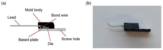
Figure 1.
Construction of an exemplary semiconductor element placed in (a) TO-220 cross-section, (b) TO-220 view.
Figure 1 shows a cross-section of a semiconductor device in a representative TO-220 case. The upper part of the case consists of a mold body, copper plate and leads. In the visible part of the copper plate, there is a screw hole that allows for the heat sink connection. There is a die inside the mold body. The die is a small block of semiconducting material on which a given functional element is fabricated [11,12]. Examples of modern semiconductor materials are silicon Si [13], silicon carbide SiC [14] and gallium nitride GaN [15]. The die is connected to the leads with a bond wire. These are thin wires with a diameter of several to several hundred micrometers. The die is connected to the leads through a copper plate.
The current flow through the semiconductor element causes heat release in the die and thus an increase in its temperature. An excessive die temperature indicates that too much power is dissipated in the die [16]. The heat released in the die is transferred by conduction to other parts of the semiconductor element [17]. Therefore, an excessively high temperature in the case indicates that too much power is dissipated in the element, which can deteriorate the operating conditions of the semiconductor element or lead to damage in extreme situations. Deterioration of the operating conditions of the semiconductor element can result in a reduction in its useful life and in the decreased energy efficiency of the device [18].
Knowledge of the die temperature under normal operating conditions allows a possible evaluation of the correctness of the semiconductor component selection and its cooling system [19]. The low die temperature (close to ambient temperature) is, on the one hand, good information (reliable operation of the semiconductor component and low power losses), and, on the other, it informs about the possible oversizing of the component and cooling system (unjustified increase in the cost of the device). On the other hand, an excessive temperature reduces the reliability of the device (and, in the worst case, it results in damaging the semiconductor component) and indicates the need for the re-selection of the semiconductor element and the cooling system [20].
During the operation of an electronic device with a semiconductor device, information about the die temperature of the semiconductor device is important. The use of the methods described in the literature requires a measurement system with varying degrees of sophistication. The more advanced the measuring system, the more effort is needed to perform the measurement. In addition, not all methods allow the temperature of the semiconductor die to be measured during its operation when it is installed on the target printed circuit board (PCB). For this reason, information was collected about the available die temperature measurement methods and they were evaluated in terms of the advancement of the measurement system and the possibility of using the semiconductor device on the target PCB during operation.
2. Methods of Measurement of Die Temperature of Semiconductor Elements
To determine the die temperature of semiconductor elements, methods from the following three groups can be used:
- -
- electrical methods [21];
- -
- contact methods [22];
- -
- non-contact methods [23].
Electrical methods are the only ones that allow direct access to the die, without the need to remove the mold body [24].
2.1. Electrical Methods for Measuring Die Temperature
2.1.1. Description
The electrical methods included in the first group of die temperature determination methods use the dependence of the selected electrical parameter on the die temperature. This parameter is called the thermal sensitive parameter (TSP). The use of the TSP is only possible for those semiconductor dies for which the relationship between the TSP value and the die temperature is known. This relationship is expressed by factor k according to Equation (1) [25].
The k factor can be determined after appropriate rescaling. For this purpose, the tested semiconductor element should be placed in a chamber with controlled internal temperature Ta. In the scaling process, it can be assumed that after a sufficiently long time interval, the set value of ambient temperature Ta = Tj. After each change in the Ta value setting and the determination of the TSP value at the set Ta values, the relationship between the TSP and Ta = Tj should be determined. To measure the value of the TSP and other signals, an analog to digital converter is usually used.
The value of the k factor obtained can be adulterated as a result of self-heating. This phenomenon results from current flow during the scaling process. There are two groups of methods that allow us to eliminate the influence of self-heating:
- pulsed mode (switching methods);
- continuous mode (non-switching methods) [26].
In switching methods, the current IF flows through the die only when the measurement is made. The measurement time TM is assumed to be short enough so that the Tj value during the measurement is close to the Tj value when the measurement is not performed. A disadvantage of the switching methods is the disturbances that arise in the measurement system as a result of switching.
These disturbances can be eliminated by using non-switching methods. In this method, the IF current flow during the rescaling process is so small that the self-heating phenomenon is minimal and can be neglected. This IF value is characteristic for a semiconductor element. It can be assumed that self-heating could be neglected when the power dissipated on the die during the Pj measurement is less than 1% of the maximum (catalogue) value dissipated on the die (Pjmax). When the value of current IF is too small, the relationship between the TSP and Tj is non-linear.
The following thermal sensitive parameters are used:
- forward voltage VF;
- threshold voltage Vth;
- bipolar transistor current gain;
- other (e.g., resistance of the drain–source channel of the transistor RDS as a TSP).
2.1.2. Forward Voltage of the Diode as a TSP
Among the TSP parameters indicated, the most frequently used is the relationship between the voltage at the VF junction, the current at the IF junction and the junction temperature Tj. This relationship is described by Equation (2) [27]:
where Ipn is the current, q is the electron charge (1.6·10−19 C), k is Boltzmann’s constant (1.381·10−23 J/K), Vpn is the voltage across the junction, Tj is the junction temperature, γ is a constant approximately equal to 3, and Eg is the band gap of Si (1.12 eV) at T = 275 K.
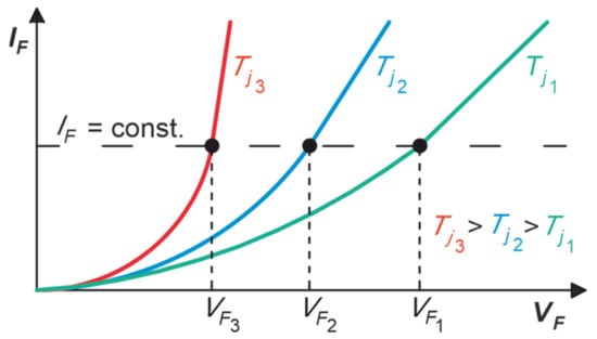
Figure 2.
Relationship between forward voltage VF and forward current IF.
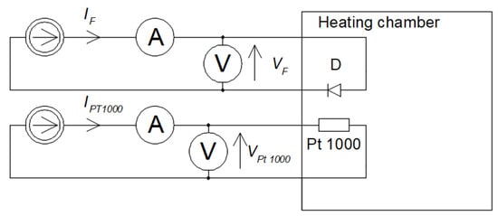
Figure 3.
Electrical circuit to determine the relationship VF = f(Tj, IF = const).
The dependence VF = f(Tj, IF = const) is linear for a wide range of IF values. When the IF value is smaller than the boundary value, the dependence VF = f(Tj, IF = const) is non-linear, as shown in Figure 3. The boundary value is characteristic for the semiconductor element [29].
Figure 4 shows the effect of self-heating caused by too much current flowing through the semiconductor. It can be seen that as the current increases, the temperature of the semiconductor element also increases. Consequently, the shape of VF = f(Tj) changes. This effect of self-heating is also evident for other TSPs.
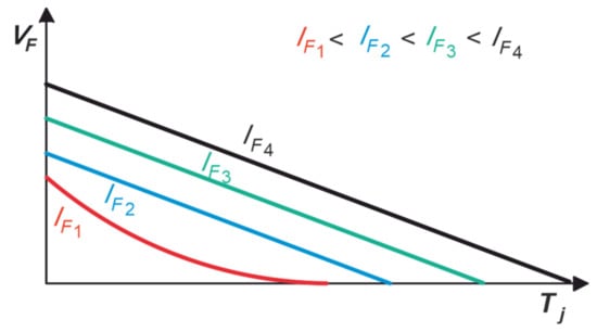
Figure 4.
Dependence of forward voltage VF on the die temperature Tj for a constant IF value.
2.1.3. Threshold Voltage of Field Effect Transistor as a TSP
The second relationship exploits the property that the threshold voltage Vth of the field effect transistor depends on the die temperature Tj, and therefore it can be used as the TSP. As the Tj value increases, the relationship between the drain current ID and the gate voltage VG changes. The Vth value can be determined using a tangent line to the ID = f(VG) characteristic at such a point that its slope and the ordinate intersection point with this tangent line are approximately equal to the slope of line that approximates the linear part of the characteristic and its ordinate intersection point. The abscissa intersection point by the tangent line allows the determination of the Vth value. The method to determine the Vth value from Tj is shown in Figure 5 [30].
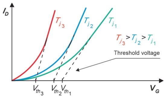
Figure 5.
Method to determine the value of threshold voltage Vth and the dependence of Vth on the die temperature Tj.
The electrical circuit that allows the designation of the relationship between drain current ID and gate voltage VG is shown in Figure 6.
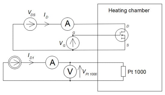
Figure 6.
Electrical circuit that allows designation of the relationship between drain current ID and gate voltage VG.
2.1.4. Bipolar Transistor Current Gain as a TSP
The third relationship uses the fact that the current gain β of bipolar transistors is a TSP. It is defined using Equation (3):
where IC and IB are the collector and base current, respectively.
The relationship between the die temperature and current gain β is complex. The value of this relationship is affected by the doping of the transistor. The effect of the temperature on the current gain β of the bipolar transistor is minimized to improve the stability and performance of the device in which the transistor is placed. The dependence of the β value on the Tj value can be observed by analyzing the relationship between current gain β and collector current IC—see Figure 7 [31].
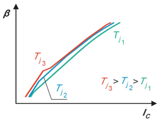
Figure 7.
Dependence of current gain β on collector current IC of the bipolar transistor.
The electrical circuit that allows the designation of the relationship between transistor gain β and collector current IC is shown in Figure 8.
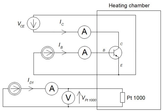
Figure 8.
Electrical circuit that allows the designation of the relationship between transistor gain β and collector current IC.
2.1.5. Other Used TSPs
Other TSPs are described in the literature. There is a known method for determining the temperature of a semiconductor diode based on the Vth value [32]. The temperature of the semiconductor structure of the unipolar transistor can be determined based on power losses [33]. It is possible to determine the temperature of a unipolar transistor based on the relationship between Tj and the resistance of the drain–source channel RDS [34]. From the TSP value of a body diode placed in the mold body of a unipolar transistor (e.g., VF, Vth), the transistor die value Tj can be determined [35]. A method is described that consists of identifying the relationship between the resistance of a single path located in the die and the Tj value. These are methods that can be implemented in the laboratory environment. Their practical application is difficult to implement and therefore is not described in this paper.
2.1.6. Summary of Electrical Methods
Electrical methods for measuring the temperature of a semiconductor die are based on the relationship between the temperature of the semiconductor die and the thermal parameter. The accuracy of these methods depends on the accuracy of the relationship determined between the TSP and die temperature. The resolution of these methods depends on the resolution of the AC/DC converter used. For this reason, in order to obtain satisfying results, these methods require an extended measurement system to be used. Additionally, using these methods to measure the temperature of the semiconductor die in an operating semiconductor device requires changing electrical circuits or using a special machine with thin spikes. For these reasons, the use of such methods for the temperature measurement of semiconductor dies in operating electronic devices is difficult.
Another disadvantage of electrical methods is the impossibility of temperature mapping on either the surface of the semiconductor component or on the surface of the case. For this reason, it is impossible to relate the temperature map to the power dissipated in the die. In addition, the use of electrical methods requires knowledge of the relationship between Tj and the TSP for the entire range of Tj. This is cumbersome, as determining the Tj = f(TSP) relationship requires additional research [36]. The relationship Tj = f(TSP) is specific for every semiconductor. For this reason, electrical methods to measure the temperatures of semiconductor devices are difficult to use outside a laboratory.
2.2. Contact Methods of Measurement of Die Temperature
2.2.1. Description of Contact Methods
The second group of methods that allow the measurement of the semiconductor die temperature are contact methods. These methods require a thermal connection between the die and the temperature sensor or between the die and liquid crystals (LC) [37]. Contact temperature measurement methods include semiconductor die temperature measurement and the measurement of semiconductor case elements. In this section, semiconductor die measurements are described. Semiconductor case temperature measurements, which are used in indirect measurements, will be described in Section 3. To conduct the measurement of the semiconductor die temperature, it is necessary to open the case, so that, without damaging the die and bond wires, the sensor (alternatively, LC) is placed directly on the die [38]. Opening the case and mounting the sensor is a difficult process and poses the risk of damaging the semiconductor element. Closing an open case to restore normal operating conditions is also difficult. Therefore, after the measurements have been made, a component with an open case is usually not suitable for further use. In addition, a die in an open case is exposed to environmental conditions that can be destructive to the semiconductor. Therefore, such a method of die temperature measurement is performed under laboratory conditions [39].
In non-laboratory applications, the sensor is applied to the case of a semiconductor element without opening it (alternatively, LC is applied to the case). However, such a measurement provides information about the case temperature, not the die temperature. In this case, the methods presented in Section 3 should additionally be used to determine the temperature of the die. Moreover, in both cases, the thermal connection of the sensor and the case (or die) can disturb the temperature distribution on the tested surface, distorting the temperature measurement results. In addition, in high-voltage circuits, contact measurement poses the risk of electrocution to the person performing the measurement, or of damaging the diagnostic equipment [40]. Regardless of the surface measured in contact methods, measurements can be carried out with the use of one of the four methods that use the following:
- thermocouple;
- liquid crystals;
- thermographic phosphor;
- thermistor and thermoresistor.
2.2.2. Thermocouple
The first method that allows die temperature measurement is one that uses a thermocouple. Thermocouple operation is based on the Seebeck phenomenon. A thermocouple consists of two different fragments of metal or metal alloys. The metals (or metal alloys) are connected to each other on one side by a weld. The other ends are not connected (free-ended). The measuring junction is applied to the die. Along with the change in the die temperature, the temperature of the measuring junction changes [41]. In turn, a change in the temperature of the measuring junction causes a change in the voltage between the free ends of the VT thermocouple.
The relationship between the VT value and the value of the weld temperature depends on the type of metal used (or metal alloys) [42]. The types of metal or metal alloy used depend on the type of thermocouple. In order for a thermocouple to work correctly, an additional system compensation circuit is required (so-called cold junction temperature compensation). One example is a system with an additional measuring circuit with a sensor (e.g., a thermistor or resistance thermometer) monitoring the actual temperature of the second junction of the thermocouple. The need for compensation and the unknown value of the weld–die thermal resistance are the main disadvantages of this method. The advantage of using a thermocouple is its wide temperature range and durability. The system utilized to measure the die with the use of a thermocouple (without a compensation system) is shown in Figure 9.
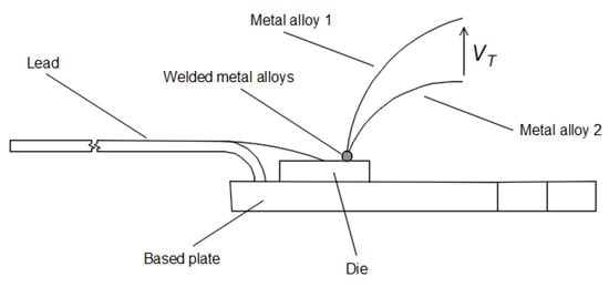
Figure 9.
Die temperature measurement using a thermocouple based on a representative case of TO-220.
2.2.3. Liquid Crystal
The second method that allows the estimation of the die temperature is one using liquid crystal (LC). This method uses the phenomenon of changing the LC phase depending on the temperature of the surfaces on which it is applied (e.g., semiconductor die). It is possible to visualize the die temperature changes by using different colors, which are assigned to the different phases of LC. This method consists of the application of LC to the die of the semiconductor device. The LC can be a component of paint applied to the die with a brush. The LC phase change is then assessed by visual perception. To visualize the temperature distribution on the tested surface of the semiconductor element [43], all types of LC can be used, including cholesteric LC (CLC), hysteresis CLC (HCLC), smectic LC (SLC), and nematic LC (NLC) [44].
It should be remembered that the use of LC is justified [45] when the phase transition temperatures do not exceed the allowable maximum die temperature Tj [46], which means that several LC phase transitions are possible within the temperature range of the semiconductor die. In this situation, the observer can register several different colors assigned to this LC phase. The number of color transitions in the temperature range is determined by the paint manufacturer.
LC-based paint can also be used to visualize the temperature distribution on the tested semiconductor die surface. Therefore, it is possible to determine the so-called hotspots, i.e., the points on the test surface of the semiconductor die whose temperature is clearly higher than the temperature of other spots on the surface [47]. In the case of searching for hotspots [48], LCs are selected in such a way that the LC phase transition temperature is as close to the hotspot temperature as possible [49]. The greatest disadvantage of this method is the price of LC paint and the limited resolution.
2.2.4. Thermographic Phosphors
The third method to determine the temperature of the die uses thermographic phosphors. This method is similar to the method using liquid crystals. It involves the application of a ceramic powder doped with rare earth elements on the tested surface. When the powder is irradiated with ultraviolet radiation, it fluoresces. The intensity of fluorescence depends on the temperature and is assessed on the basis of visual perception. The intensity of this phenomenon decreases as the surface temperature increases [50]. This method is successfully used to measure the temperature of electronic devices [51].
2.2.5. Thermistor and Thermoresistor
The last and fourth method of contact temperature measurement for a semiconductor element is the use of a thermistor and a thermoresistor. Due to the large dimensions of a thermistor or thermoresistor case compared to a die, there have been no reported attempts to use these sensors to measure the die temperature (the performance of such a sample measurement is unknown to the authors).
However, these elements have been successfully used for measuring the temperature of a semiconductor case. Next, this semiconductor case temperature is used in indirect die temperature measurement (see Section 3). The thermistor differs from the thermoresistor in the shape of the relationship between sensor resistance RS and temperature TC. For the operating temperature range of semiconductor devices (from −55 °C to 150 °C), the relationship is RS = f(TC) for both types of thermistors, and the negative temperature coefficient (NTC) and positive temperature coefficient (PTC) are strongly non-linear—see Figure 9 [52].
For the same temperature range (−55 °C to 150 °C), the shape of the relationship RS = f(TC) for a thermoresistor is approximately a linear function. The relationship RS = f(TC) for the Pt 1000 thermoresistor is shown in Figure 10 [53].
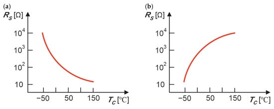
Figure 10.
Relationship between sensor resistance RS and case temperature TC of the semiconductor device, where temperature is measured for (a) thermistor NTC, (b) PTC.
Gluing a Pt 1000 sensor to a semiconductor device case causes a local temperature change in the mold body around the glued sensor. The same problem can be observed with a thermistor bonded to a semiconductor case. There is a problem with the unknown value of the thermal resistance between the semiconductor case and the sensor case (thermistor or thermoresistor). This problem can be solved by using an adhesive with a known thermal resistance value. The way in which the Pt 1000 sensor is connected to the measuring circuit is also important. A two-wire circuit and a four-wire circuit are used—Figure 11. The four-wire connection is used to compensate for the resistance of the Rw wires. The means of connecting the two-wire and four-wire thermoresistors are shown in Figure 12.
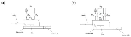
Figure 11.
Cross-section of representative TO 220 case with Pt 1000 sensor glued in (a) two-wire circuit and (b) four-wire circuit. The proportions of the dimensions have not been maintained.
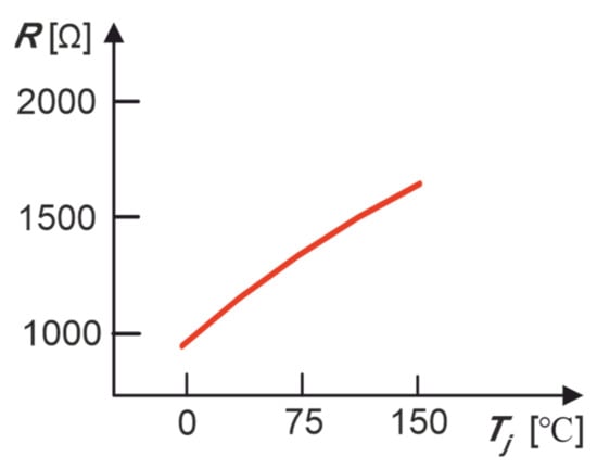
Figure 12.
Relationship between sensor resistance RS and case temperature TC of a semiconductor device whose temperature is measured.
The greatest difficulty in this temperature measurement method is to ensure adequate thermal resistance between the temperature sensor (thermistor, thermoresistor) and the semiconductor case. To limit the temperature variation of the semiconductor case (when measuring its temperature), it is necessary to use a temperature sensor in the smallest possible case. Gluing a temperature sensor in a small case (e.g., a thermoresistor placed in a Surface-Mounted Device 0603 case) to a small semiconductor case is difficult. Soldering wires to this sensor case is also difficult. The advantages of this temperature measurement method are the easy access to thermistors and thermoresistors and the extensive descriptions of the use of these sensors that can be found in the literature.
2.2.6. Summary of Contact Methods
Contact methods for die temperature measurement do not require the use of complicated measurement systems. Their use is simple and fast. Additionally, the resolution of these methods is high. Some of these methods (thermographic phosphor and liquid crystal) allow the temperature to be mapped on the surface of a semiconductor die (or the surface of a semiconductor case) with high resolution (in the order of a few micrometers).
These methods exploit fundamental physics phenomena, such as the temperature dependence of resistance or the changes in material properties at different temperatures. Some of them (e.g., thermocouples) use additional devices that allow simple temperature measurement based on the non-linear characteristics of the thermocouple. The main disadvantage of these methods is the unknown thermal resistance between the temperature sensor and the surface of the semiconductor die (or the temperature of the semiconductor case).
An additional disadvantage is the possibility of electric shock and the inability to directly measure the temperature of the semiconductor die while the device is operating (without damaging the case). These methods allow for the contact temperature measurement of the semiconductor case. Based on this measurement and the methods described in Section 3, it is possible to estimate the temperature of the semiconductor during device operation. The thermal resolution, advantages and disadvantages of all the described methods for the contact temperature measurement of the semiconductor die are summarized in Table 1.

Table 1.
Summarized thermal resolutions, advantages and disadvantages of all described contact methods for measuring semiconductor die temperature.
2.3. Non-Contact Methods of Measurement of Die Temperature
2.3.1. Description
Non-contact die temperature measurements require, as in contact methods, that the case of the semiconductor element should be opened. The temperature is determined by the observation of the die without applying any elements to it. Nevertheless, this method of measurement, similarly to contact methods, is used in a laboratory environment. The use of a non-contact method means that there is no direct contact with the tested surface (e.g., semiconductor die), and the method does not affect the temperature distribution on the surface [62]. However, pyrometric and thermographic measurements, despite their apparent simplicity, have certain limitations and difficulties resulting from the measurement conditions [63] and the properties of semiconductor devices [64]. In addition, in the case of measuring the case temperature, its result informs us about the temperature of the case rather than the die. This raises the fundamental question of the difference between the die temperature and the temperature of the observed case surface. During pyrometric and thermal imaging measurements, it is necessary to know the values of the parameters characterizing the observed surface, particularly the emissivity coefficient, and to assess the impact of the environment on the measurement result [65].
From a practical point of view, the die temperature assessment based on the non-contact measurement of the case temperature is the most optimal solution to be used in the diagnostics of operating electronic devices [66]. It should be emphasized that such a measurement requires competence in the use of pyrometers and thermal imaging cameras, as well as knowledge of the phenomena occurring during the measurement. Considering the above, non-contact methods include measurements using:
- a pyrometer or thermal imaging camera;
- thermoreflectance—a change in the value of the reflection coefficient;
- luminescence.
2.3.2. Thermographic and Pyrometric Measurement of Die Temperature
The die temperature can be estimated from the surface temperature of the case measured with a pyrometer. This non-contact method consists of the detection of infrared radiation emitted from the observed surface (e.g., semiconductor die). Then, due to the physical phenomena occurring in the detector under the influence of IR radiation incident on the detector surface and based on its intensity value, the die surface temperature can be determined.
The increase in the Tj value causes an increase in the temperature value of the tested surface (Ts) and, as a result, an increase in the spectral emittance W of IR radiation emitted from this surface. The increase in the Tj value also causes a shift in the maximum wave of emitted radiation λmax towards shorter wavelengths, in accordance with Wien’s law (Equation (4)) [67]:
where λmax—the maximum wavelength of emitted radiation (µm).
Assuming an operating temperature range of the die semiconductor element between −55 and 175 °C, a corresponding wave range of 13.28 to 6.47 can be determined based on Equation (1). This is the wave range corresponding to the LWIR sub-band. Knowledge of the IR sub-band facilitates the selection of the type of IR detector.
An important value of the observed surface that must be known in order to obtain a correct measurement is coefficient ε. In general terms, this coefficient is the ratio of the radiation emitted by a black body to the radiation emitted by the observed surface under the same conditions, i.e., at the same temperature and at the same angle [68]. In addition to these indicated factors, the ε value of die depends on:
- the material from which the observed surface is made;
- the condition of the die (e.g., clean, dirty, scratched);
- the observation angle;
- the temperature of the die surface observed [69].
The value of the emissivity coefficient can be read from tables available in the literature. This value can also be measured. The known emissivity of another surface, placed as close as possible to the surface whose emissivity is being measured, should be set on the thermal imaging camera. The temperature of both surfaces should be the same. The temperature surface with the known emissivity should then be measured. In the last step, we observe the surface with unknown emissivity and change the set emissivity so that the temperature measurement value of both surfaces is the same. The result of the temperature measurement of the semiconductor die depends on the selected value of the emissivity coefficient. If the selected emissivity coefficient value differs from the actual emissivity coefficient value, the measured temperature value may be subject to error. The relationship between the set emissivity coefficient value and the measured Tjm temperature of the semiconductor die is shown in Figure 13.
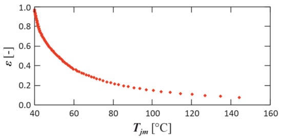
Figure 13.
Dependence between the set value of emissivity coefficient ε and the measured semiconductor die Tjm in the same semiconductor temperature.
The pyrometer allows for the non-contact temperature measurement of a single point. It is impossible to obtain a temperature distribution over the entire test surface of the die. For this reason, thermal imaging cameras equipped with infrared detector arrays are used to measure the die temperature. The dies used can differ in the type of detector and spatial resolution and they can have different spectral ranges. As mentioned, the spectral range of the waves mimicked by the semiconductor element coincides with the LWIR sub-range. For this reason, two types of IR radiation detectors are most commonly used:
- microbolometer;
- detector based on Strained Layer Superlattice (SLS).
The microbolometer (one pixel from an array of uncooled detectors) is an IR detector whose resistance increases as the intensity of IR radiation incident on the detector surface increases. Roughly, it is a square with a side of approximately 17 µm [70]. The microbolometer sensor does not require cooling, which increases the application area of a camera using the sensor [71]. It usually works in the long wave infrared (LWIR) band. The microbolometer time constant is approximately 20 ms [72]. For this reason, obtaining a high measurement frequency (above 50 frames per second) with the use of microbolometer arrays is impossible. There are commercially available cameras with arrays of microbolometer sensors that allow for the measurements to be taken at a frequency of 80 fps (frames per second). This is possible in measurements performed when the detector is not stabilized. The method of obtaining such a measurement frequency using a microbolometer sensor is commercially confidential and it is not described by manufacturers [73].
The third group of the mentioned Strained Layer Superlattice (SLS) detectors operate on the basis of superlattices. These are detectors operating in the LWIR and MWIR bands [74]. Their greatest advantage is the integration time (depending on the selected temperature range) from 0.028 ms to 0.16 ms. As a consequence, it is possible to obtain a high measurement frequency in the order of thousands fps (frames per second). Dies based on these detectors are characterized by a high spatial resolution in the order of megapixels. The greatest advantages of SLS detectors can be seen when their operation is limited to the LWIR band (with the use of filters). Compared to other detectors operating in this band, it is possible to improve the measurement frequency, homogeneity and stability [75].
Due to the wavelength, SLS-based detectors can also be used. Regardless of the type of detector used, thermograms recorded with a thermal imaging camera can be sent via a USB (or Ethernet) interface to a computer with appropriate software installed. This allows for the further processing and storage of thermograms. Often, when measuring the temperature of electronic components, the thermal imaging camera is placed on a tripod. This makes it possible to obtain a stable thermogram (no hand vibrations) and a constant distance between the observed surface and the thermographic camera lens. A diagram showing the measurement system consisting of a thermal imaging camera, a tripod and a computer is shown in Figure 14.
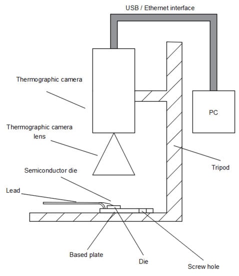
Figure 14.
The use of thermal imaging cameras to measure the die temperature of a semiconductor element.
The temperature of the semiconductor die Tj resulting from the thermogram depends on the conditions prevailing at the time of measurement. The value of thermal imaging temperature measurement is affected by the emissivity coefficient ε [76], reflected temperature Tr [77], distance between the lens and the observed object d [78], ambient temperature Ta [79], transmittance of the atmosphere τa, temperature of the external optical system Tl [80], transmittance of the external optical system τl [81] and relative humidity ω [82]. In addition, the thermographically measured die temperature depends on the viewing α [83], and the sharpness of the recorded thermogram Tus [84].
Based on research carried out, it has been proven that in thermographic temperature measurements of the die surfaces of semiconductor elements Tj, when the distance between the die and the lens of the thermal imaging camera is small (in the order of millimeters), ω and τa have the smallest impact on the camera indication. In turn, τl, Tus and α have the largest influence. The distance d also has a great influence on the result of thermal imaging temperature measurement Tj. This is the case when a macro lens is used, and when this type of lens is applied, even a small change in d, in the order of tenths of a micrometer, affects the indication of the thermal imaging camera and reduces the sharpness of the recorded thermogram. This is due to the shallow depth of field of the lens. The correct sharpness can only be obtained for the value of d = WD (work distance) specified by the manufacturer. For the distance d used in thermal imaging measurements of the surface temperatures of semiconductor elements (d < 1 m), the value of τa is close to 1 [85,86].
2.3.3. Thermoreflectance
Another method to determine the die temperature uses the change in the refractive index of radiation caused by the die temperature change [87]. The method that uses this property relies on measuring the relative change in the reflectance of the material as a function of the material temperature. The reflectance change depends on the wavelength of incident radiation, the properties of the material and its surface and the ambient temperature. For temperatures in the range of temperature Tj, the value of the reflectance coefficient (thermal reflectance) can be considered constant [88]. The relative change in optical reflectance with the temperature is quite small, being in the order of 10−5 K−1 to 10−4 K−1.
The measurement system allowing for the measurement of the surface temperature based on the dependence of the reflectance coefficient on the temperature is shown in Figure 15.
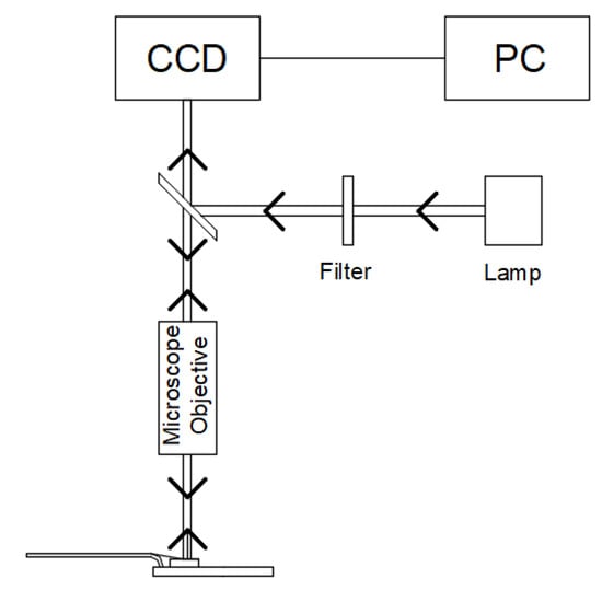
Figure 15.
The measurement system allowing for the measurement of surface temperature based on the dependence of reflectance coefficient on temperature.
2.3.4. Luminescence
Temperature measurement on the semiconductor die surface is also possible using the phenomenon of luminescence. This phenomenon is caused by external stimulation—for example, an electric field or by photo-excitation. As a result of the recombination of electrons and holes (with the peak energy occurring in direct band gap materials at the band gap energy), radiation is emitted. There are two types of luminescence: electroluminescence and photoluminescence. In the first case, electrons and holes are injected through the pn junction. In photoluminescence, the source of electrons and holes is external optical excitation. This method has a limitation: it is only useful for measuring the temperature of the direct band gap semiconductors. An example of this type of semiconductor is GaAs. Descriptions of electroluminescence and photoluminescence for the temperature measurement of complex semiconductor devices can be found in the literature. The resolution of the photoluminescence method can be 1 °C [89].
2.3.5. Summary of Non-Contact Methods
Non-contact methods of measuring the temperature of a semiconductor die eliminate some hazards, such as electric shock. They do not require the electrical circuit to be changed during the temperature measurement. This is a major advantage when the temperature of a semiconductor element is measured while the semiconductor is in operation. This group of methods also has disadvantages. These include the need for knowledge of the various phenomena occurring during the measurement and knowledge of the influence of external conditions on the temperature measurement result (this is particularly evident in thermography). Another disadvantage is the high cost of equipment (e.g., a thermal imaging camera with an SLS-based IR detector)—Table 2.
Table 2.
Summarized thermal resolutions, advantages and disadvantages of all described non-contact methods to measure semiconductor die temperature.
3. Determination of Die Temperature Based on the Case Temperature
The methods that are described in Section 2.2 and Section 2.3 allow the surface temperature to be measured. The die temperature of the semiconductor element is located inside the housing. In order to estimate the die temperature of a semiconductor element on the basis of the known temperature of the case (measured by contact and non-contact methods), one of the methods described below must be used.
3.1. Die–Case Thermal Resistance
The simplest method to determine the value of Tj from the measured value of TC is based on comparing a thermal circuit to an electrical circuit. In this comparison, the electric potential V corresponds to the temperature T, the electric current corresponds to the heat flux, and the electrical resistance R corresponds to the thermal resistance θjc. The general relationship between the values of Tj, TC and θjc is described in Equation (5) [97].
where θjc is the junction–case thermal resistance; Pj = VI is the power dissipation on the die.
In practical solutions, the thermal impedance or Zth function Zθjc(t) is determined instead of θjc. For a semiconductor device that is heated with a constant value of Pj, for starting time t = 0, and while its case surface is properly connected to the heat sink, the value of Zθjc(t) can be defined by Equation (6) [98].
A method that enables the determination of the value of θjc is the Transient Dual Interface Measurement method mentioned in the JEDEC standards [99]. This method could be applied for semiconductor devices with a heat flow through a single path—a high conductive heat flow path from the die surface (that is heated) to a package case surface, which can connect it to an external heat sink. Changing the cooling conditions in the semiconductor package does not affect the thermal impedance value until the temperature in the case starts to rise. Then, the impact is revealed at the point where there is contact with the heat sink. When the value of the resistance of this contact is different, the total thermal resistance at the steady state also changes. For this reason, the impedance curves from the point at which external contact resistance makes an impact have different waveforms. The cumulative thermal resistance at the point of separation of the curves obtained for different contact resistance values is defined as θjc [98].
In practice, the value of transient thermal resistance Zth is often used. The value of Zth(t) at the steady state is equal to the thermal resistance Rth [100]. In order to determine the Zth value for a semiconductor diode, a method with two current sources, measuring IM and heating IH, can be used. In order to use this method, three steps must be performed: calibration, heating and cooling. The diode under the test is placed in the thermostat.
In the first step, a calibration curve is determined. An IM current of a suitably selected value flows through a diode polarized in the conduction direction and slowly changes inside the thermostat (with this, the temperature of the diode changes). As a consequence, it is possible to estimate the slope F of the thermometric characteristic curve. The forward voltage VF is used as the TSP during the flow of the IM current [101].
In the second step, the selected thermostat temperature is set. A high IH current (IH >> IM) flows through the diode tested. The temperature of the tested diode increases. This step ends when the thermal steady state of the diode under the test is reached. At the end of this step, the voltage across the VH diode is recorded.
The cooling stage (step 3) starts at t = 0, when the current IH stops flowing through the tested diode. During this step, a small IM current flows through the diode. Measurements of the forward voltage of the tested diode vF(t) are recorded until the steady state is reached. In [102], it is assumed that Zth can be determined as follows:
When determining the Zth value for MOSFET transistors, a forward voltage body diode can be used as a TSP. For IGBT transistors, the gate-emitter voltage VGE can be used as a TSP [103] or an anti-parallel diode VD [104] can be used.
The Zth value can be obtained as a result of simulation work. This is possible, for example, using the SPICE MultiSIM software. On their websites, the manufacturers of semiconductor devices often offer free models of such devices, which can be easily implemented in the applied software. The time required to obtain an accurate Zth waveform is long. For this reason, the piecewise linear electrical circuit simulation (PLECS) method can be used for the simulation work, which enables thermal modeling using the parameters of a linear RC circuit (Cauer or Foster). In [105], it was proposed to use this method to determine the Zth value of an Insulated Gate Bipolar Transistor (IGBT).
3.2. Finite Element Method
3.2.1. Natural Convection
The Tj value can be determined based on the known TC value and the thermal conductivity of the mold body. The difference in both temperatures Tj and Tc in the x-direction can also be determined using Equation (8) [106]:
where q is radiative heat flux in W/m2, and k is thermal conductivity W/m·K.
After separating the variables and integrating Equation (8) on both sides, determining the time constant, when q penetrates the semiconductor case, Equation (8) takes the form of Equation (9):
where T1 is the temperature at the starting point of the analyzed heat flow path (K), T2 is the temperature at the end point of the analyzed heat flow path (K), P is the total power applied to the selected wall, S is the total area of the selected wall and x is the path of the analyzed heat flow.
Relating the equation under consideration to the case of heat dissipation in the housing of a semiconductor element, Equation (9) can be written as Equation (10):
where Tj is the semiconductor die temperature (K), TC is the semiconductor case temperature and S is the total area of the selected semiconductor wall.
In practice, the temperature distribution obtained in one line (1D model) might not provide enough data. In addition, dividing the distance between the die and the casing (mold body) in one part only allows an approximate temperature difference to be obtained. For this reason, a 3D model is used to obtain more information. Numerical methods are used to obtain the temperature distribution in a solid (e.g., in the case of a semiconductor component, a 3D model). One of them is the finite element method (FEM). In the FEM method, the solid in which the temperature distribution is sought is divided into tetrahedral elements. In each tetrahedral element, the temperature field is interpolated based on the temperature at the nodes of that element and linear shape functions—see Equation (11) [107]:
where Ti(t) is the nodal temperature at node i, and Hi is the linear shape function.
In consequence, it is possible to determine the difference between the semiconductor die temperature and the case temperature. In addition, it is possible to determine the difference between the case temperature and the heat sink temperature and between the semiconductor die temperature and the heat sink temperature. These calculations are time-consuming. For this reason, they are realized in a dedicated computer program, e.g., Solidworks, Comsol or Ansys. They are also possible in Matlab (with the Partial Differential Equation Toolbox).
Once the temperature differences have been determined, it is possible to evaluate the die temperature based on the measured temperature of the case or heat sink. The accuracy of the die temperature estimation depends on the accuracy of the determination of the temperature distribution on the surface of the housing or heat sink. The correct mapping of the temperature distribution on the surface of a semiconductor element requires knowledge of the amount of heat emitted by convection and by radiation. The amount of heat emitted by radiation per unit of time and unit of area is determined by the radiation coefficient hr, which can be obtained using Equation (12) [108]:
where σc is the Stefan–Boltzmann constant, equal to 5.67 × 10⁻⁸ (W∙m−2∙K−4); TS is the surface temperature (K), and Ta is the air temperature (K).
The amount of heat emitted by convection per unit time and per unit area is determined by the convection coefficient hc. The hc coefficient is selected using the theory of similarity to physical phenomena. The relationships with the physical quantities that characterize the phenomenon are described using the Nusselt, Grashof and Prandtl criteria. When calculating the value of the convection coefficient for a flat area, Equation (13) is used [109]:
where hc is the convection coefficient of flat surfaces, Nu is the Nusselt number (-), and L is the characteristic length in meters (for a vertical wall, it is the height).
The Nusselt number is described by Equation (14) [110]:
where a and b are dimensionless coefficients, the values of which depend on the shape and orientation of the analyzed surface; the product Pr·Gr. Pr (-) is the Prandtl number, and Gr (-) is the Grashof number.
The Prandtl number can be obtained using Equation (15) [28]:
where c is the specific heat of air equal to 1005 (J∙kg−1∙K−1) in 293.15 (K), and η is the dynamic air viscosity equal to 1.75 × 10⁻⁵ (kg∙m−1∙s−1) in 273.15 (K).
The Grashof number can be obtained using Equation (16) [28]:
where α is a the coefficient of expansion equal to 0.0034 (K−1), g is the gravitational acceleration of 9.8 (m∙s−2), and ρ is the air density equal to 1.21 (kg∙m−3) in 273.15 (K).
After inserting the result of Equation (14) into Equation (13), the value of the convection coefficient for natural convection can be calculated.
3.2.2. Forced Convection
The method presented above for calculating the convection coefficient (Equations (12)–(15)) is only reasonable for natural convection. This type of convection occurs when the air surrounding the semiconductor case is not moving. When the air around the semiconductor case is moving (e.g., through the cooling system), the convection is referred to as “forced convection”. In this situation, it is also possible to apply the theory of similarity to physical phenomena, but some of the equations are different. The calculation of the convection coefficient for forced convection is shown below. The convection coefficient for forced convection can be determined from Equation (17).
where Nu (-)—Nuselt number, Pr (-)—Prandtl number, Re (-)—Reynolds number, C, a, b—coefficients depending on Reynolds number, C, a, b—coefficients depending on surface orientation (horizontal/vertical) and type of airflow (turbulent/laminar).
The Prandtl number can be obtained in the same way as for natural convection (Equation (15)). The Reynolds number can be obtained from Equation (18).
where V (m/s) is the average linear velocity of fluid flow.
Using Equations (13)–(18) (and the FEM method), it is possible to determine the Tj value based on the measured value of Tc, if the values of hc, hr, the properties of the semiconductor case (e.g., thermal conductivity) and the temperature of the case Tc (measured by the contact or optical method, described in Section 2.2 and Section 2.3) are known. This indirect measurement of the semiconductor die temperature has been described in the literature.
It has been shown that the difference between the semiconductor case temperature measured and the semiconductor case temperature obtained from simulations (performed with the methods presented in this paper) is approximately a few degrees Celsius (less than 5 °C). The semiconductor die temperature obtained by this method (indirect temperature measurement) has also been shown to be reliable [111].
4. Discussion
Access to the die requires that the mold body should be damaged. Electronic instruments with a damaged mold body cannot be used in an electronic device. For this reason, in practical applications, it is more common to use methods in which a temperature sensor is applied to the case of a semiconductor instrument and then the temperature of the die is determined from the measured temperature of the case.
Some of the methods presented only allow point measurements. Examples of such methods are contact methods (Section 2.2), which use an appropriately selected temperature sensor. With these methods, it is not possible to map the temperature distribution on the surface of the semiconductor element or die. In addition, applying a metal sensor to the die surface of a semiconductor device can cause damage to the die. It is also dangerous, as there is a risk of electrocution during the measurement.
The preparation of a temperature distribution map by contact methods is possible with the use of liquid crystals and thermographic phosphors. These methods only allow the evaluation of the temperature distribution on the surface of a semiconductor device or die based on visual perception. The thermal resolution of both methods is low and only approximate temperature determination is possible (see Table 1 and Table 2). Therefore, both of these methods are better suited for checking whether the temperature limit has been reached, rather than determining the temperature with specific (required) accuracy.
The mapping of the temperature distribution on the tested surface based on non-contact methods is possible with the use of thermography. Similar to a pyrometer, a thermal imaging camera records infrared radiation emitted from the observed surface. Then, as a result of physical processes taking place in the detector, an electrical signal appears at its terminals, the value of which corresponds to the temperature of the observed surface. Unlike a pyrometer, a thermal imaging camera has an array of thermal imaging detectors.
The spatial resolution of the temperature distribution of the image recorded on the examined surface depends on the spatial resolution of the detector array used. The spectral range of waves, which corresponds to the temperature range of the semiconductor die, corresponds to the LWIR sub-band.
Uncooled microbolometers and other IR detectors based on SLS technology operate in the LWIR sub-band. Uncooled microbolometers are larger. For this reason, arrays built with an SLS-based IR detector have a higher spatial resolution. Obtaining the most accurate temperature distribution on the surface under investigation is possible using a thermal imaging camera equipped with SLS detectors [112,113,114].
The accuracy of thermographic temperature measurement is lower compared to the accuracy of measurement performed using contact methods (see tables). Furthermore, the accuracy of thermographic temperature measurement depends on the conditions prevailing during the measurement. Depending on the intensity of factors affecting the value of thermographic temperature measurement, the accuracy of the measurement changes.
Another problem related to thermal imaging temperature measurement is determining the correct value of emissivity coefficient ε. The ε value depends, among others, on the condition of the observed surface and the material from which it is made. It is also dependent on the temperature of the object observed.
The measurement conducted with some non-contact methods is faster than measurement using contact methods involving the application of a temperature sensor. In the case of contact methods, heat from the tested surface is transferred to the sensor by conduction. In addition, there is unknown thermal resistance between the surface and the temperature sensor.
Heat energy is transferred to infrared sensors by means of infrared radiation, which, not unlike visible radiation, is an electromagnetic wave. The propagation speed of infrared radiation is close to the speed of light. For this reason, heat transfer via infrared radiation is faster than heat transfer by thermal conduction.
Non-contact methods are more expensive compared to contact methods. Their implementation requires the use of more advanced measuring equipment. The final price of the measurement system depends, among others, on the type of sensors used and the technical capabilities (among others, measurement frequency and spatial resolution). In the case of indirect optical methods (semiconductor case measured by optical methods and semiconductor die temperature estimated on the basis of this measurement and FEM), the measured case temperature should be related to the die temperature, taking into account the properties of the case material.
Electrical methods constitute a separate group. The advantage of electrical methods is access to the semiconductor die without having to remove the mold body. The use of electrical methods is troublesome as it requires knowledge of the relationship between the TSP value and the die temperature value. The relation between the TSP value and die temperature is specific to the semiconductor element. Determination of this relationship is possible after prior scaling for this element. This makes the method difficult to apply in practice. For this reason, electrical methods are more difficult to apply compared to contact methods and non-contact methods.
As regards measurements using contact and non-contact methods outside the laboratory, it is worth noting that, in this case, there is no direct access to the semiconductor element. For this reason, the die temperature is determined from the case temperature. This is enabled by information on the die–case thermal resistance. This information can be found in the item’s catalogue note. The use of this method additionally requires knowledge of the power dissipated in the die. For this reason, the practical use of this method is difficult.
5. Conclusions
Among the contact methods, the use of liquid crystals and the luminescence phenomenon is described. Both methods are suitable for mapping the temperature distribution, and their resolution allows for the detection of instances of exceeding the threshold temperature of the observed surface. The use of contact methods, involving the application of temperature sensors to the die of the semiconductor element, allows for the determination of the die temperature with high resolution and accuracy (see Table 1). However, their use can damage the semiconductor die. It is also dangerous because there is a possibility of electric shock.
Non-contact methods make it possible to eliminate these risks. In addition to pyrometer measurement, these methods yield a map of the temperature distribution on the tested surface with high spatial resolution. The accuracy of these methods is lower than the accuracy of the contact method (see Table 2). The result obtained by non-contact methods is affected by external conditions. The use of non-contact methods requires a more expensive measuring system compared to contact methods.
In practical applications outside the laboratory environment, access to the semiconductor die is possible only after damaging the case or as a result of using electrical methods. These are methods that allow the determination of the die temperature value on the basis of a predetermined characteristic that links this value to the value of a thermal sensitive parameter (TSP). Determination of this characteristic requires removal of the semiconductor element from the electronic device. For this reason, the use of these methods outside the laboratory environment is difficult.
Reliable measurement of the case temperature by contact and non-contact methods is possible with the use of commonly available equipment. On the basis of the case temperature measured in this way, it is possible to determine the die temperature. However, this requires the use of appropriate analysis methods that combine both of these temperatures, e.g., the FEM method. Based on the analyzed methods presented in this article, it is possible to ascertain that the best temperature measurement method (for measuring semiconductor die temperature during operation) is the indirect method. For this measurement, it is proposed to use FEM and thermographic temperature measurement of the semiconductor case.
Author Contributions
Literature review, K.D., A.H. and G.W.; literature analysis, K.D. and A.H.; investigation, K.D., A.H. and P.K.; resources, K.D.; writing—original draft preparation, K.D., A.H., P.K. and G.W.; writing—review and editing, K.D., A.H., P.K. and G.W.; visualization, K.D.; supervision, K.D. and A.H. All authors have read and agreed to the published version of the manuscript.
Funding
This research was supported by statutory funds from the Faculty of Control, Robotics and Electrical Engineering of the Poznan University of Technology.
Institutional Review Board Statement
Not applicable.
Informed Consent Statement
Not applicable.
Data Availability Statement
Not applicable.
Conflicts of Interest
The authors declare no conflict of interest.
References
- Joglekar, C.; Mortimer, B.; Ponci, F.; Monti, A.; De Doncker, R.W. SST-Based Grid Reinforcement for Electromobility Integration in Distribution Grids. Energies 2022, 15, 3202. [Google Scholar] [CrossRef]
- Alghaythi, M.L.; O’Connell, R.M.; Islam, N.E.; Guerrero, J.M. A multiphase-interleaved high step-up DC-DC boost converter with voltage multiplier and reduced voltage stress on semiconductors for renewable energy systems. In Proceedings of the IEEE Power & Energy Society Innovative Smart Grid Technologies Conference (ISGT), Washington, DC, USA, 17–20 February 2020. [Google Scholar] [CrossRef]
- Nikolic, M.V.; Milovanovic, V.; Vasiljevic, Z.Z.; Stamenkovic, Z. Semiconductor Gas Sensors: Materials, Technology, Design, and Application. Sensors 2020, 20, 6694. [Google Scholar] [CrossRef] [PubMed]
- Bhalerao, S.R.; Lupo, D.; Berger, P.R. Flexible, solution-processed, indium oxide (In2O3) thin film transistors (TFT) and circuits for internet-of-things (IoT). Mater. Sci. Semicond. Process. 2022, 139, 106354. [Google Scholar] [CrossRef]
- Kalsoom, T.; Ramzan, N.; Ahmed, S.; Ur-Rehman, M. Advances in Sensor Technologies in the Era of Smart Factory and Industry 4.0. Sensors 2020, 20, 6783. [Google Scholar] [CrossRef]
- Sasaki, M.; Ikeda, M.; Asada, K. A Temperature Sensor With an Inaccuracy of −1/+0.8 °C Using 90-nm 1-V CMOS for Online Thermal Monitoring of VLSI Circuits. IEEE Trans. Semicond. Manuf. 2008, 21, 201–208. [Google Scholar] [CrossRef]
- Sun, L.; Shi, Z.; Wang, H.; Zhang, K.; Dastan, D.; Sun, K.; Fan, R. Ultrahigh discharge efficiency and improved energy density in rationally designed bilayer polyetherimide–BaTiO 3/P (VDF-HFP) composites. J. Mater. Chem. A 2020, 8, 5750–5757. [Google Scholar] [CrossRef]
- Minh, Q.N.; Nguyen, V.-H.; Quy, V.K.; Ngoc, L.A.; Chehri, A.; Jeon, G. Edge Computing for IoT-Enabled Smart Grid: The Future of Energy. Energies 2022, 15, 6140. [Google Scholar] [CrossRef]
- Martins, L.S.; Guimarães, L.F.; Junior, A.B.B.; Tenório, J.A.S.; Espinosa, D.C.R. Electric car battery: An overview on global demand, recycling and future approaches towards sustainability. J. Environ. Manag. 2021, 295, 113091. [Google Scholar] [CrossRef]
- Bu, Z.; Zhang, X.; Hu, Y.; Chen, Z.; Lin, S.; Li, W.; Xiao, C.; Pei, Y. A record thermoelectric efficiency in tellurium-free modules for low-grade waste heat recovery. Nat. Commun. 2022, 13, 237. [Google Scholar] [CrossRef]
- Jacques, S.; Diack, P.M.; Batut, N.; Leroy, R.; Gonthier, L. Rise time and dwell time impact on Triac solder joints lifetime during power cycling. In Proceedings of the 27th International Conference on Microelectronics Proceedings, Nis, Serbia, 16–19 May 2010. [Google Scholar] [CrossRef]
- Recommendations for Board Assembly of Infineon Transistor Outline Type Packages. Available online: https://www.infineon.com/dgdl/InfineonRecommendations_for_Board_Assembly_TO-P-v03_00-EN.pdf?fileId=5546d462580663ef0158069840880338 (accessed on 5 December 2022).
- Bhol, K.; Jena, B.; Nanda, U. Silicon nanowire GAA-MOSFET: A workhorse in nanotechnology for future semiconductor devices. Silicon 2022, 14, 3163–3171. [Google Scholar] [CrossRef]
- Ramkumar, M.S.; Priya, R.; Rajakumari, R.F.; Valsalan, P.; Chakravarthi, M.K.; Latha, G.; Mathupriya, S.; Rajan, K. Review and Evaluation of Power Devices and Semiconductor Materials Based on Si, SiC, and Ga-N. J. Nanomater. 2022, 2022, 8648284. [Google Scholar] [CrossRef]
- Hashimoto, T.; Letts, E.R.; Key, D. Progress in Near-Equilibrium Ammonothermal (NEAT) Growth of GaN Substrates for GaN-on-GaN Semiconductor Devices. Crystals 2022, 12, 1085. [Google Scholar] [CrossRef]
- Niu, H. A review of power cycle driven fatigue, aging, and failure modes for semiconductor power modules. In Proceedings of the 2017 IEEE International Electric Machines and Drives Conference (IEMDC), Miami, FL, USA, 21–24 May 2017. [Google Scholar] [CrossRef]
- Nol Chen, J.; Zhang, X. Prediction of thermal conductivity and phonon spectral of silicon material with pores for semiconductor device. Phys. B Condens. Matter 2021, 614, 413034. [Google Scholar] [CrossRef]
- Moore, A.L.; Shi, L. Emerging challenges and materials for thermal management of electronics. Mater. Today 2014, 17, 163–174. [Google Scholar] [CrossRef]
- Górecki, K.; Posobkiewicz, K. Cooling Systems of Power Semiconductor Devices—A Review. Energies 2022, 15, 4566. [Google Scholar] [CrossRef]
- Balda, J.C.; Mantooth, A. Power-Semiconductor Devices and Components for New Power Converter Developments: A key enabler for ultrahigh efficiency power electronics. IEEE Power Electron. Mag. 2016, 3, 53–56. [Google Scholar] [CrossRef]
- Bercu, N.; Lazar, M.; Simonetti, O.; Adam, P.M.; Brouillard, M.; Giraudet, L. KPFM-Raman Spectroscopy Coupled Technique for the Characterization of Wide Bandgap Semiconductor Devices. Mater. Sci. Forum 2022, 1062, 330–334. [Google Scholar] [CrossRef]
- Avenas, Y.; Dupont, L.; Khatir, Z. Temperature measurement of power semiconductor devices by thermo-sensitive electrical parameters—A review. IEEE Trans. Power Electron. 2011, 27, 3081–3092. [Google Scholar] [CrossRef]
- Abad, B.; Borca-Tasciuc, D.A.; Martin-Gonzalez, M.S. Non-contact methods for thermal properties measurement. Renew. Sustain. Energy Rev. 2017, 76, 1348–1370. [Google Scholar] [CrossRef]
- Zhang, B.; Chen, S.; Lu, G.Q.; Mei, Y.H. Reliability Behavior of A Resin-Free Nanosilver Paste at Ultra-Low Temperature of 180 °C. Power Electron. Devices Compon. 2022, 3, 100014. [Google Scholar] [CrossRef]
- JESD 51-53. Available online: https://www.jedec.org (accessed on 5 December 2022).
- Blackburn, D.L. A Review of Thermal Characterization of Power Transistors. In Proceedings of the 4th Annual IEEE Semiconductor Thermal and Temperature Measurement Symposium, San Diego, CA, USA, 6 August 2002. [Google Scholar] [CrossRef]
- Baliga, J. Modern Power Devices; John Wiley and Sons, Inc.: Hoboken, NJ, USA, 1987. Available online: https://www.osti.gov/biblio/6719122 (accessed on 5 December 2022).
- Poppe, A.; Farkas, G.; Gaál, L.; Hantos, G.; Hegedüs, J.; Rencz, M. Multi-Domain Modelling of LEDs for Supporting Virtual Prototyping of Luminaires. Energies 2019, 12, 1909. [Google Scholar] [CrossRef]
- Khatir, Z. Junction Temperature Investigations Based on a General Semi-analytical Formulation of Forward Voltage of Power Diodes. IEEE Trans. Electron Devices 2012, 59, 1716–1722. [Google Scholar] [CrossRef]
- Sun, Q.J.; Gao, X.; Wang, S.D. Understanding temperature dependence of threshold voltage in pentacene thin film transistors. J. Appl. Phys. 2013, 113, 194506. [Google Scholar] [CrossRef]
- Yang, E.S.; Yang, Y.F.; Hsu, C.C.; Ou, H.J.; Lo, H.N. Temperature dependence of current gain of GaInP/GaAs heterojunction and heterostructure-emitter bipolar transistors. IEEE Trans. Electron Devices 1999, 46, 320–323. [Google Scholar] [CrossRef]
- Threshold Voltahe Data Analysis. Available online: https://electronics.stackexchange.com/questions/333725/threshold-voltage-data-analysis (accessed on 5 December 2022).
- Barlini, D.; Ciappa, M.; Mermet-Guyennet, M.; Fichtner, W. Measurement of the transient junction temperature in MOSFET devices under operating conditions. Microelectron. Reliab. 2007, 47, 1707–1712. [Google Scholar] [CrossRef]
- Koenig, A.; Plum, T.; Fidler, P.; De Doncker, R. On-line Junction Ternperature Measurernent of CoolMOS Devices, Power Electronics and Drive Systems. In Proceedings of the 7th International Conference on Power Electronics and Drive Systems, Bangkok, Thailand, 27–30 November 2007. [Google Scholar] [CrossRef]
- Yan, D.; Ma, D.B. A Monolithic GaN Power IC With On-Chip Gate Driving, Level Shifting, and Temperature Sensing, Achieving Direct 48-V/1-V DC–DC Conversion. IEEE J. Solid State Circuits 2022, 57, 3865–3876. [Google Scholar] [CrossRef]
- Lv, Y.; Yin, S.; Liu, Y.; Li, Z.; Li, P.; Sun, X.; Chen, J.; Yang, Z.; Yuan, J. Continuously Geometric Phase Modulation by using a reflective liquid crystal structure. Opt. Commun. 2022, 509, 127847. [Google Scholar] [CrossRef]
- Soldati, A.; Delmonte, N.; Cova, P.; Concari, C. Device-Sensor Assembly FEA Modeling to Support Kalman-Filter-Based Junction Temperature Monitoring. IEEE J. Emerg. Sel. Top. Power Electron. 2019, 7, 1736–1747. [Google Scholar] [CrossRef]
- Salem, T.E.; Ibitayo, D.; Geil, B.R. A Technique for Die Surface Temperature Measurement of High-Voltage Power Electronic Components using Coated Thermocouple Probes. In Proceedings of the 2006 IEEE Instrumentation and Measurement Technology Conference Proceedings, Sorrento, Italy, 24–27 April 2006. [Google Scholar] [CrossRef]
- Weil, E.D.; Levchik, S. A review of current flame retardant systems for epoxy resins. J. Fire Sci. 2004, 22, 25–40. [Google Scholar] [CrossRef]
- Dziarski, K.; Hulewicz, A.; Dombek, G.; Drużyński, Ł. Indirect Thermographic Temperature Measurement of a Power-Rectifying Diode Die. Energies 2022, 15, 3203. [Google Scholar] [CrossRef]
- Jeon, J.G.; Kim, H.J.; Shin, G.; Han, Y.; Kim, J.H.; Lee, J.H.; Lee, J.; Lim, H.; Ha, S.; Bae, M.; et al. High-Precision Ionic Thermocouples Fabricated Using Potassium Ferri/Ferrocyanide and Iron Perchlorate. Adv. Electron. Mater. 2022, 8, 2100693. [Google Scholar] [CrossRef]
- Lima, H.V.; Campidelli, A.F.; Maia, A.A.; Abrão, A.M. Temperature assessment when milling AISI D2 cold work die steel using tool-chip thermocouple, implanted thermocouple and finite element simulation. Appl. Therm. Eng. 2018, 143, 532–541. [Google Scholar] [CrossRef]
- Srodit, G.; Szabon, J.; Janossy, I.; Azekely, V. High Resolution Thermal Mapping of Microcircuits Using Nematic Liquid Crystals. Solid State Electron. 1981, 24, 1127–1133. [Google Scholar] [CrossRef]
- Popov, V.M.; Klimenko, A.S.; Pokanevich, A.P.; Gavrilyuk, I.I.; Moshel, N.V. Liquid-crystal thermography of hot spots on electronic components. Russ. Microelectron. 2007, 36, 392–401. [Google Scholar] [CrossRef]
- Park, J.H.; Lee, C.C. A new configuration of nematic liquid crystal thermography with applications to GaN-based devices. IEEE Trans. Instrum. Meas. 2006, 55, 273–279. [Google Scholar] [CrossRef]
- Fleuren, E.M. A Very Sensitive and Simple Analytic Technique Using Nematic Liquid Crystals. In Proceedings of the 21st Annual International Reliability Physics Symposium, Phoenix, AZ, USA; 1983; pp. 148–149. [Google Scholar]
- Lee, C.C.; Park, J. Temperature measurement of visible light-emitting diodes using nematic liquid crystal thermography with laser illumination. IEEE Photonics Technol. Lett. 2004, 16, 1706–1708. [Google Scholar] [CrossRef]
- Burgess, D.; Tan, R. Improved Sensitivity for Hot Spot Detection Using Liquid Crystal. In Proceedings of the 22nd Annual Reliability Physics Symposium, Las Vegas, NV, USA, 3–5 April 1984; pp. 119–121. [Google Scholar] [CrossRef]
- Hiatt, J.A. A Method for Detection of Hot Spots on Semiconductors Using Liquid Crystals. In Proceeding of the 19th Annual Reliability Physics Symposium, Orlando, FL, USA, 7–9 April 1981; pp. 130–133. [Google Scholar] [CrossRef]
- Aldén, M.; Omrane, A.; Richter, M.; Särner, G. Thermographic phosphors for thermometry: A survey of combustion applications. Prog. Energy Combust. Sci. 2011, 37, 422–461. [Google Scholar] [CrossRef]
- Brübach, J.; Pflitsch, C.; Dreizler, A.; Atakan, B. On surface temperature measurements with thermographic phosphors: A review. Prog. Energy Combust. Sci. 2013, 39, 37–60. [Google Scholar] [CrossRef]
- A Simple Thermistor Design for Industrial Temperature Measurement. Available online: http://repository.futminna.edu.ng:8080/jspui/handle/123456789/10291 (accessed on 5 December 2022).
- SIMOTICS GP/SD/DP/XP Low-Voltage Motors—1LE1 Platform Release for Sale and Delivery: Product Has Been Extended to Include Pt1000 Resistance Thermometer. Available online: https://support.industry.siemens.com/cs/document/109741861/simotics-gp-sd-dp-xp-low-voltage-motors-%E2%80%93-1le1-platform-release-for-sale-and-delivery-product-has-been-extended-to-include-pt1000-resistance-thermometer-?dti=0&lc=en-AT (accessed on 5 December 2022).
- Emaikwu, N.; Catalini, D.; Muehlbauer, J.; Hwang, Y.; Takeuchi, I.; Radermacher, R. Experimental investigation of a staggered-tube active elastocaloric regenerator. Int. J. Refrig. 2022. [Google Scholar] [CrossRef]
- Yen Kee, Y.; Asako, Y.; Lit Ken, T.; Che Sidik, N.A. Uncertainty of Temperature measured by Thermocouple. J. Adv. Res. Fluid Mech. Therm. Sci. 2020, 68, 54–62. [Google Scholar] [CrossRef]
- Moller, S.; Resagk, C.; Cierpka, C. On the application of neural networks for temperature field measurements using thermochromic liquid crystals. Exp. Fluids 2020, 61, 111. [Google Scholar] [CrossRef]
- Cai, T.; Li, Y.; Guo, S.; Peng, D.; Zhao, X.; Liu, Y. Pressure effect on phosphor thermometry using Mg4FGeO6:Mn. Meas. Sci. Technol. 2019, 30, 027001. [Google Scholar] [CrossRef]
- Platinum Temperature Sensor PT1000-55—Data Sheet. Available online: https://www.tme.eu/Document/67cf717905f835bc5efcdcd56ca3a8e2/Pt1000-550_EN.pdf (accessed on 18 January 2023).
- Temperature Sensors Pt100/Pt1000 Series—Technical Data. Available online: http://www.image.micros.com.pl/_dane_techniczne_auto/cz%20pt1000-4x32b%20ii.pdf (accessed on 18 January 2023).
- Thermistor Thermal Resolution—PDF. Available online: https://www.pdffiller.com/jsfiller-desk11/?requestHash=0ad693dd27755969522e5d1dd32d20714f957bf6b310e8966402229ae42ecc79&projectId=1193607408&loader=tips&MEDIUM_PDFJS=true&PAGE_REARRANGE_V2_MVP=true&isPageRearrangeV2MVP=true#1fe3cca8891a4c83b3a27c2c60c28ffe (accessed on 18 January 2023).
- NTC Thermistors—Application Note. Available online: https://www.vishay.com/docs/29053/ntcappnote.pdf (accessed on 18 January 2023).
- Hulewicz, A.; Dziarski, K.; Dombek, G. The Solution for the Thermographic Measurement of the Temperature of a Small Object. Sensors 2021, 21, 5000. [Google Scholar] [CrossRef]
- Minkina, W.; Dudzik, S. Infrared Thermography: Errors and Uncertainties; John Wiley & Sons: Hoboken, NJ, USA, 2009. [Google Scholar]
- Legierski, J.; Wiecek, B. Steady state analysis of cooling electronic circuits using heat pipes. IEEE Trans. Compon. Packag. Technol. 2001, 24, 549–553. [Google Scholar] [CrossRef]
- Dziarski, K.; Hulewicz, A.; Dombek, G. Lack of Thermogram Sharpness as Component of Thermographic Temperature Measurement Uncertainty Budget. Sensors 2021, 21, 4013. [Google Scholar] [CrossRef]
- Felczak, M.; Więcek, B.; De Mey, G. Optimal placement of electronic devices in forced convective cooling conditions. Microelectron. Reliab. 2009, 49, 1537–1545. [Google Scholar] [CrossRef]
- Santamaría-Holek, I.; Pérez-Madrid, A. Scaling Planck’s law: A unified approach to the Casimir effect and radiative heat-conductance in nanogaps. Nanoscale Horiz. 2022, 7, 526–532. [Google Scholar] [CrossRef]
- Zampoli, V.; Jordan, P.M. Second-sound phenomena in type II conductors with Stefan–Boltzmann source. Mech. Res. Commun. 2022, 126, 103998. [Google Scholar] [CrossRef]
- Litwa, M. Influence of angle of view on temperature measurements using thermovision camera. IEEE Sens. J. 2010, 10, 1552–1554. [Google Scholar] [CrossRef]
- Ajmera, S.K.; Syllaios, A.J.; Tyber, G.S.; Taylor, M.F.; Hollingsworth, R.E. Amorphous silicon thin-films for uncooled infrared microbolometer sensors. In Proceedings of the Infrared Technology and Applications XXXVI, Orlando, FL, USA, 5–9 April 2010. [Google Scholar] [CrossRef]
- Yadav, P.K.; Yadav, I.; Ajitha, B.; Rajasekar, A.; Gupta, S. Reddy, Advancements of Uncooled Infrared Microbolometer Materials: A Review. Sens. Actuators A Phys. 2022, 342, 113611. [Google Scholar] [CrossRef]
- Dufour, D.; Le Noc, L.; Tremblay, B.; Tremblay, M.N.; Généreux, F.; Terroux, M.; Vachon, C.; Wheatley, M.J.; Johnston, J.M.; Wotton, M.; et al. Bi-Spectral Microbolometer Sensor for Wildfire Measurement. Sensors 2021, 21, 3690. [Google Scholar] [CrossRef] [PubMed]
- Optris Xi 400. Available online: https://www.optris.global/optris-xi-400?gclid=Cj0KCQiAyracBhDoARIsACGFcS6QywUcVtRWJEML-YW59PMjbauQd65cIBKpFHuxnjYOj37Mq3LMuGsaAmvKEALw_wcB (accessed on 5 December 2022).
- Gurga, A.R.; Nosho, B.Z.; Terterian, S.; Wang, S.; Rajavel, R.D. Dual-band MWIR/LWIR focal plane arrays based on III-V strained-layer superlattices. In Proceedings of the Infrared Technology and Applications XLIV, Orlando, FL, USA, 15–19 April 2018. [Google Scholar] [CrossRef]
- The Advantages of LWIR SLS Thermal Cameras. Available online: http://www.flirmedia.com/MMC/THG/Brochures/RND_077/RND_077_US.pdf (accessed on 5 December 2022).
- Zaccara, M.; Edelman, J.B.; Cardone, G. A general procedure for infrared thermography heat transfer measurements in hypersonic wind tunnels. Int. J. Heat Mass Transf. 2020, 163, 120419–120435. [Google Scholar] [CrossRef]
- Altenburg, S.J.; Straße, A.; Gumenyuk, A.; Maierhofer, C. In-situ monitoring of a laser metal deposition (LMD) process: Comparison of MWIR, SWIR and high-speed NIR thermography. Quant. InfraRed Thermogr. J. 2020, 19, 97–114. [Google Scholar] [CrossRef]
- Yoon, S.T.; Park, J.C. An experimental study on the evaluation of temperature uniformity on the surface of a blackbody using infrared cameras. Quant. InfraRed Thermogr. J. 2021, 19, 172–186. [Google Scholar] [CrossRef]
- Schuss, C.; Remes, K.; Leppänen, K.; Saarela, J.; Fabritius, T.; Eichberger, B.; Rahkonen, T. Detecting Defects in Photovoltaic Cells and Panels with the Help of Time-Resolved Thermography under Outdoor Environmental Conditions. In Proceedings of the 2020 IEEE International Instrumentation and Measurement Technology Conference (I2MTC), Dubrovnik, Croatia, 25–28 May 2020; pp. 1–6. [Google Scholar] [CrossRef]
- Chakraborty, B.; Sinha, B.K. Process-integrated steel ladle monitoring, based on infrared imagin—A robust approach to avoid ladle breakout. Quant. InfraRed Thermogr. J. 2020, 17, 169–191. [Google Scholar] [CrossRef]
- Tomoyuki, T. Coaxiality Evaluation of Coaxial Imaging System with Concentric Silicon–Glass Hybrid Lens for Thermal and Color Imaging. Sensors 2020, 20, 5753. [Google Scholar] [CrossRef]
- Wollack, J.E.; Cataldo, G.; Miller, K.H.; Quijada, A.M. Infrared properties of high-purity silicon. Opt. Lett. 2020, 45, 4935–4938. [Google Scholar] [CrossRef]
- Dziarski, K. Selection of the Observation Angle in Thermography Temperature Measurements with the Use of a Macro Lens. In Proceedings of the 13th International Conference on Measurement, Bratislava, Slovakia, 17–19 May 2021. [Google Scholar] [CrossRef]
- Dziarski, K.; Hulewicz, A. Effect of unsharpness on the result of thermovision diagnostics of electronic components. In Proceedings of the 15th Quantitative InfraRed Thermography Conference, Porto, Portugal, 6–10 July 2020. [Google Scholar] [CrossRef]
- Minkina, W.; Klecha, D. Atmospheric transmission coefficient modelling in the infrared for thermovision measurement. J. Sens. Sens. Syst. 2016, 5, 17–23. [Google Scholar] [CrossRef]
- Dziarski, K.; Hulewicz, A. Uncertainty of Thermographic Temperature Measurement of Electric Units Contained in Switchgear. Pomiary Autom. Robot. 2021, 25, 31–36. [Google Scholar] [CrossRef]
- Wang, D.; Zheng, L.; Si, W.; Yang, H.; Gao, Y. Thermal Analysis of High-Power Light-Emitting Diode Using Thermoreflectance Thermography. In Proceedings of the 2021 22nd International Conference on Electronic Packaging Technology (ICEPT), Xiamen, China, 14–17 September 2021; pp. 1–4. [Google Scholar] [CrossRef]
- Thermo-Reflectance Thermography for Submicron Temperature Measurements. Available online: https://www.electronics-cooling.com/2008/02/thermo-reflectance-thermography-for-submicron-temperature-measurements/ (accessed on 18 January 2023).
- Blackburn, D.L. Temperature measurements of semiconductor devices—A review. In Proceedings of the Twentieth Annual IEEE Semiconductor Thermal Measurement and Management Symposium (IEEE Cat. No.04CH37545), San Jose, CA, USA, 11 March 2004; pp. 70–80. [Google Scholar] [CrossRef]
- González-Aguilera, D.; Rodriguez-Gonzalvez, P.; Armesto, J.; Lagüela, S. Novel approach to 3D thermography and energy efficiency evaluation. Energy Build. 2012, 54, 436–443. [Google Scholar] [CrossRef]
- Sensors, S. Infrared Camera Accuracy and Uncertainty in Plain Language. Available online: https://www.fierceelectronics.com/components/infrared-camera-accuracy-and-uncertainty-plain-language (accessed on 18 January 2023).
- Pyrometer Testing and Heat Measurements. Available online: https://www.govinfo.gov/content/pkg/GOVPUB-C13-37e7fd57919420ec99a37e4d43a952f3/pdf/GOVPUB-C13-37e7fd57919420ec99a37e4d43a952f3.pdf (accessed on 18 January 2023).
- Koskelo, E.; Radunskaya, A.; Hudgings, J. Using noise to stochastically enhance the resolution of charge coupled device based thermoreflectance imaging. J. Appl. Phys. 2020, 128, 104502. [Google Scholar] [CrossRef]
- Wang, J.; Xie, Z.; Che, X. Development of a Novel Pyrometer by Eliminating the Uncertainty of Emissivity Using Reflector with Two Apertures in Medium Plate Rolling Process. Actuators 2022, 11, 188. [Google Scholar] [CrossRef]
- Infrared Camera Accuracy and Uncertainty in Plain Language. Available online: https://www.flir.com/discover/rd-science/infrared-camera-accuracy-and-uncertainty-in-plain-language/ (accessed on 18 January 2023).
- Kopeć, M.; Więcek, B. AC temperature estimation of power electronic devices using 1D thermal modeling and IR thermography measurements. In Proceedings of the 15th Quantitative InfraRed Thermography Conference, Porto, Portugal, 20–23 September 2020; Available online: https://qirt.gel.ulaval.ca/archives/qirt2020/papers/161.pdf (accessed on 18 January 2023).
- Incropera, F.; De Witt, D. Introduction to Heat Transfer; Wiley: New York, NY, USA, 1985; Available online: https://scirp.org/reference/referencespapers.aspx?referenceid=1503886 (accessed on 5 December 2022).
- JESD 51-14. Available online: https://www.jedec.org/standards-documents, (accessed on 11 February 2023).
- Schweitzer, D.; Pape, H.; Chen, L.; Kutscherauer, R.; Walder, M. Transient dual interface measurement—A new JEDEC standard for the measurement of the junction-to-case thermal resistance. In Proceedings of the 2011 27th Annual IEEE Semiconductor Thermal Measurement and Management Symposium, San Jose, CA, USA, 20–24 March 2011; pp. 222–229. [Google Scholar] [CrossRef]
- Schweitzer, D.; Pape, H.; Chen, L. Transient measurement of the junction-to-case thermal resistance using structure functions: Chances and limits. In Proceedings of the 2008 Twenty-Fourth Annual IEEE Semiconductor Thermal Measurement and Management Symposium, San Jose, CA, USA, 16–20 March 2008. [Google Scholar] [CrossRef]
- Górecki, K.; Ptak, P. New Method of Measurements Transient Thermal Impedance and Radial Power of Power LEDs. IEEE Trans. Instrum. Meas. 2020, 69, 1. [Google Scholar] [CrossRef]
- Górecki, P.; Górecki, K.; Kisiel, R.; Myśliwiec, M. Thermal Parameters of Monocrystalline GaN Schottky Diodes. IEEE Trans. Electron Devices 2019, 66, 5. [Google Scholar] [CrossRef]
- Górecki, K.; Zarębski, J.; Górecki, P.; Ptak, P. Compact thermal models of semiconductor devices: A Review. Int. J. Electron. Telecommun. 2019, 65, 151–158. [Google Scholar] [CrossRef]
- Górecki, P.; Górecki, K. Measurements and Computations of Internal Temperatures of the IGBT and the Diode Situated in the Common Case. Electronics 2021, 10, 210. [Google Scholar] [CrossRef]
- Górecki, P.; Wojciechowski, D. Accurate Computation of IGBT Junction Temperature in PLECS. IEEE Trans. Electron. Devices 2020, 67, 7. [Google Scholar] [CrossRef]
- Devloo, P.R.B.; Bravo, C.M.A.A.; Rylo, E.C. Systematic and generic construction of shape functions for p-adaptive meshes of multidimensional finite elements. Comput. Methods Appl. Mech. Eng. 2009, 198, 1716–1725. [Google Scholar] [CrossRef]
- Staton, D.A.; Cavagnino, A. Convection heat transfer and flow calculations suitable for electric machines thermal models. IEEE Trans. Ind. Electron. 2008, 55, 3509–3516. [Google Scholar] [CrossRef]
- Ghahfarokhi, P.S. Determination of Forced Convection Coefficient over a Flat Side of Coil. In Proceedings of the 2017 IEEE 58th International Scientific Conference on Power and Electrical Engineering of Riga Technical University (RTUCON), Riga, Latvia, 12–13 October 2017. [Google Scholar] [CrossRef]
- Aminu, Y.; Ballikaya, S. Thermal resistance analysis of trapezoidal concentrated photovoltaic–Thermoelectric systems. Energy Convers. Manag. 2021, 250, 114908. [Google Scholar] [CrossRef]
- Garcia-Gutierrez, L.M.; Hernández-Jiménez, F.; Cano-Pleite, E.; Soria-Verdugo, A. Experimental evaluation of the convection heat transfer coefficient of large particles moving freely in a fluidized bed reactor. Int. J. Heat Mass Transf. 2020, 153, 119612. [Google Scholar] [CrossRef]
- Omer, K.; Butcher, C.; Worswick, M. Characterization of heat transfer coefficient for non-isothermal elevated temperature forming of metal alloys. Int. J. Mater. Form. 2020, 13, 177–201. [Google Scholar] [CrossRef]
- Flir E-Series Thermographic Cameras. Available online: https://www.flirmedia.com/MMC/THG/Brochures/IND_002/IND_002_EN.pdf (accessed on 18 January 2023).
- Flir a8580 Thermographic Camera. Available online: https://www.flir.com/products/a8580-sls/ (accessed on 18 January 2023).
- Flir x6980 Thermographic Camera. Available online: https://www.flir.com/products/x6980-sls/?vertical=rd+science&segment=solutions (accessed on 18 January 2023).
Disclaimer/Publisher’s Note: The statements, opinions and data contained in all publications are solely those of the individual author(s) and contributor(s) and not of MDPI and/or the editor(s). MDPI and/or the editor(s) disclaim responsibility for any injury to people or property resulting from any ideas, methods, instructions or products referred to in the content. |
© 2023 by the authors. Licensee MDPI, Basel, Switzerland. This article is an open access article distributed under the terms and conditions of the Creative Commons Attribution (CC BY) license (https://creativecommons.org/licenses/by/4.0/).