Article

Pulse Width Modulation-Controlled Switching Impedance for Wireless Power Transfer

College of Information Science and Engineering, Wuhan University of Science and Technology, Wuhan 430081, China
*
Author to whom correspondence should be addressed.
Energies 2023, 16(24), 8103; https://doi.org/10.3390/en16248103
Submission received: 1 November 2023 / Revised: 14 December 2023 / Accepted: 15 December 2023 / Published: 16 December 2023
(This article belongs to the Section F: Electrical Engineering)

Abstract

:
The exceptional performance of the wireless power transfer (WPT) system hinges on its resonant state. However, the capacitance drift caused by manufacturing tolerance and temperature will result in a state of detuning. In this manuscript, a PWM-controlled switched impedance (PCSI) topology that can express inductive and capacitive is proposed to eliminate line mismatches resulting from the above factors. Firstly, the PCSI topology is introduced, and its placement is determined based on the characteristics of the inductor–capacitor–capacitor series (LCC-S) network. Secondly, the working principle of the proposed topology is introduced. Finally, the simulation and experimental results show that the system could be restored to its resonant state by adjusting the PCSI topology. Under different values of resonant capacitors, the PCSI topology enhances the output power of the system by 40 W~150 W compared to the previous state, and the efficiency is increased by 9~13%.

1. Introduction

Wireless power transfer (WPT) presents numerous advantages, offering a more convenient, efficient, and secure method of energy transmission for both modern lifestyles and industrial applications. It uses coupling coils to transmit energy through a relatively large air gap while being free of cable constraints [1]. The technology is already widely used in smartphones, biomedical engineering, and electric vehicle charging. This technology can mitigate safety risks like cable failure, short circuits, or plug damage, particularly during high switching frequency and power. WPT systems realize the convenience of wireless charging by eliminating the costs associated with fraying wires and connectors [2]. At the same time, the whole system has a certain degree of spatial freedom and electrical isolation, and it relies on inductive coupling coils to transmit power between the air gap and carry out power transmission in harsh environments [3]. It can also mitigate safety risks like cable failure, short circuits, or plug damage, particularly during high-frequency and high-power transmissions. Therefore, the transmission power of the system also reaches several power levels based on its different operating frequencies and transmission distance. It can eliminate the need for plugging and unplugging cables or connectors, and the charging device can transmit energy without direct physical contact, offering a more convenient and flexible charging approach.
In the WPT system, different line topologies represent different line output characteristics. The common topologies include Series-Series (S-S), Series-Parallel (S-P), Parallel-Series (P-S), and Parallel-Parallel (P-P), which generally have disadvantages such as high sensitivity and non-adjustable output voltage. Many experts have proposed high-order resonant networks, which are different from these common topologies [4]. For example, the LCC-S resonant network has a larger resonant capacity, lower frequency drift, and reduced current/voltage stress of switching devices compared to the traditional S-S topology. All of the compensation networks require the participation of resonant elements, like a resonant capacitor. Thus, the resonant capacitor plays a very important role in the resonant circuit of the whole WPT system. To enhance the output power of the whole system and maintain a resonant state, both the primary side and the secondary side need series or parallel resonant capacitors to guarantee system efficiency. In practical applications, the transmission efficiency of the entire circuit is slightly lower than the ideal state due to the frequency control, component tolerances, and parameters [5]. In addition, due to the non-ideal soft switching state of power electronic devices such as MOSFET tubes, it may cause additional switching loss [6]. Simultaneously, when the system works at a higher frequency, the resonant capacitor will be offset due to the high temperature. Specifically, the value of the resonant capacitor changes due to temperature change, and the negative drift is more noticeable than the positive drift [7]. For example, the negative drift of Y5V materials can reach up to −80% drift. This would cause serious detuning, thereby reducing the transmission power and efficiency of the entire system.

1.1. Related Work

In order to deal with the detuning problem of the WPT system caused by the parameter change in resonant elements, there are many tuning methods for the above cases.
(1)
Switched capacitor: In [8], a self-tuning power supply uses a switching capacitor array to tune the main power supply. This new capacitor matrix can reconfigure impedance by itself and track the best impedance matching points at different distances. However, it will affect the volume of the whole system if it is too large. Meanwhile, the whole system will only be tuned discretely. In [9], a switching control capacitor (SCC) is proposed to compensate for the load impedance related to coil coupling coefficient and load change. However, this control needs signals of voltage and current obtained by the RF modules to work, which requires the system to have more precise clock synchronization. In [10], it proposes a novel switching control capacitor for wireless power transfer (WPT) that achieves variable capacitance and optimizes efficiency. But the signal from each SCC needs to be modulated byzero-crossing detection, which necessitates more accurate current sensors and comparators. The authors of [11] introduce an enhanced LCC-S compensated IPT system featuring variable frequency switching capacitor control. The tuning process involves communication modules connected in series with an extra capacitor and compensating inductor. But the inclusion of the RF module increases the overall cost of the system. Additionally, the system incorporates an excessive number of resonant energy storage components, leading to increased losses. In [12], this paper proposes a self-tuning power transmission system that utilizes switch-controlled capacitors on both the primary and secondary sides. While Wi-Fi communication is not mandatory, magnetic shielding is employed to enhance the power factor of the entire system, thereby escalating the construction cost.
(2)
Recently, a semiactive rectifier (SAR) has been used to deal with detuning. In [13,14], an active variable reactance rectifier is employed to offset the coupling change between the two systems. However, inductors are introduced to ensure impedance matching during rectifier integration. The inclusion of energy storage inductors leads to a predominant portion of the system’s losses occurring in these components. Additionally, the issue of circulating current in the parallel loop is noteworthy, contributing to increased system control complexity. In [15], this paper employs an impedance decoupling algorithm to address bilateral capacitance drift. The reactance can be eliminated by adjusting the system frequency and the phase shift angle of the active rectifier. However, it is noteworthy that this paper exclusively addresses the phenomenon of negative drift in the resonant capacitor and neglects the occurrence of positive drift, indicating a lack of generality.
(3)
A variable reactor is also used to deal with the detuning problem. In [16], the variable reactor is proposed to eliminate the cross-interference among the transmitters under multiple transmitters. However, this method compensates for the detuning of the resonant frequency owing to natural tolerance and cross-interference among the transmitters. In [17], it proposes a pure electronic resonant frequency regulation circuit that does not require any complex control and can realize the problems of long transmission distance and coil misalignment. However, this circuit is applied to systems with high Q values. But it also provides a basis for further research. On this basis, in [18], this paper introduces a novel 6.78 MHz multiplex transmitter featuring a straightforward active variable reactance component known as an Automatic Tuning Auxiliary Circuit (ATAC). The entire system requires an envelope detector to measure current outcomes. This necessitates a higher level of communication channel integrity; otherwise, it could impact the overall system performance.

1.2. Innovation and Contribution

Considering the overall design of the system and other factors, this manuscript proposes a communication-less WPT system with a series compensator topology that has no complicated controls. The proposed topology conception comes from reference [19]: synchronous series compensator (SSC). This topology is capacitive or inductive, and the excess reactance in the line only by controlling the duty cycle of SSC. A reactance control program is analyzed so that it can be performed after line detuning in this study. The LCC-S compensation network is used because its coil current is constant and not affected by the load or the coupling system. The major contributions of this paper are:
(1)
When implementing the proposed topology in the LCC-S topological network, the additional circuits mentioned in the previous literature are automatically assigned specific positions. However, the rationale for their placement is not analyzed. This paper rigorously examines the specific placement of the PCSI circuit.
(2)
In the case of capacitive or inductive detuning, adjusting the output voltage phase of the proposed topology is sufficient to bring the system back to its resonant state, ensuring optimal performance. This approach offers straightforward control without requiring Wi-Fi, RF modules, or other forms of communication.
(3)
The proposed topology not only provides a broader range of adjustments but also addresses the issue of simultaneous drift in two resonant capacitors.
This paper is organized as follows: In the second section, the PCSI circuit is analyzed theoretically. The position of the proposed topology is determined after analyzing the characteristics of the LCC-S compensation network system. Then, the basic working principle of PCSI topology is introduced. The third section presents the verification of the proposed topology through simulation and experimental results. The fourth part is a summary.

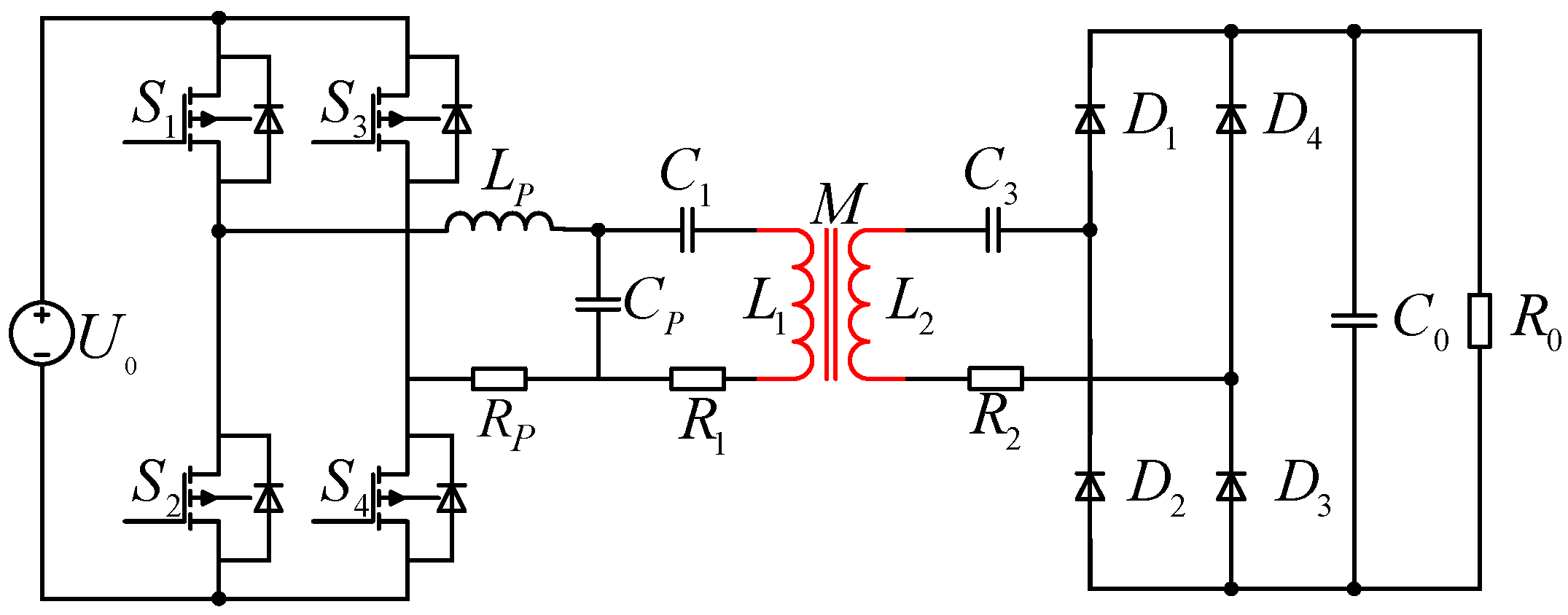
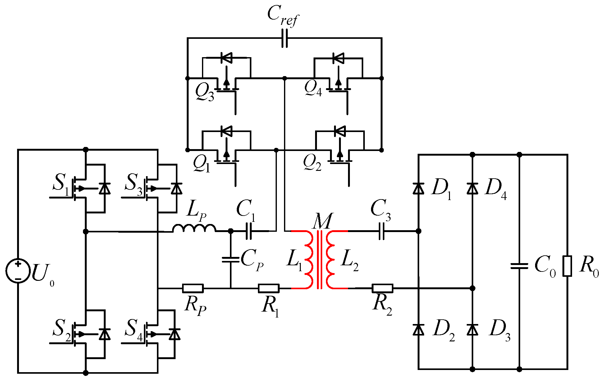
2. WPT System with PCSI Topology
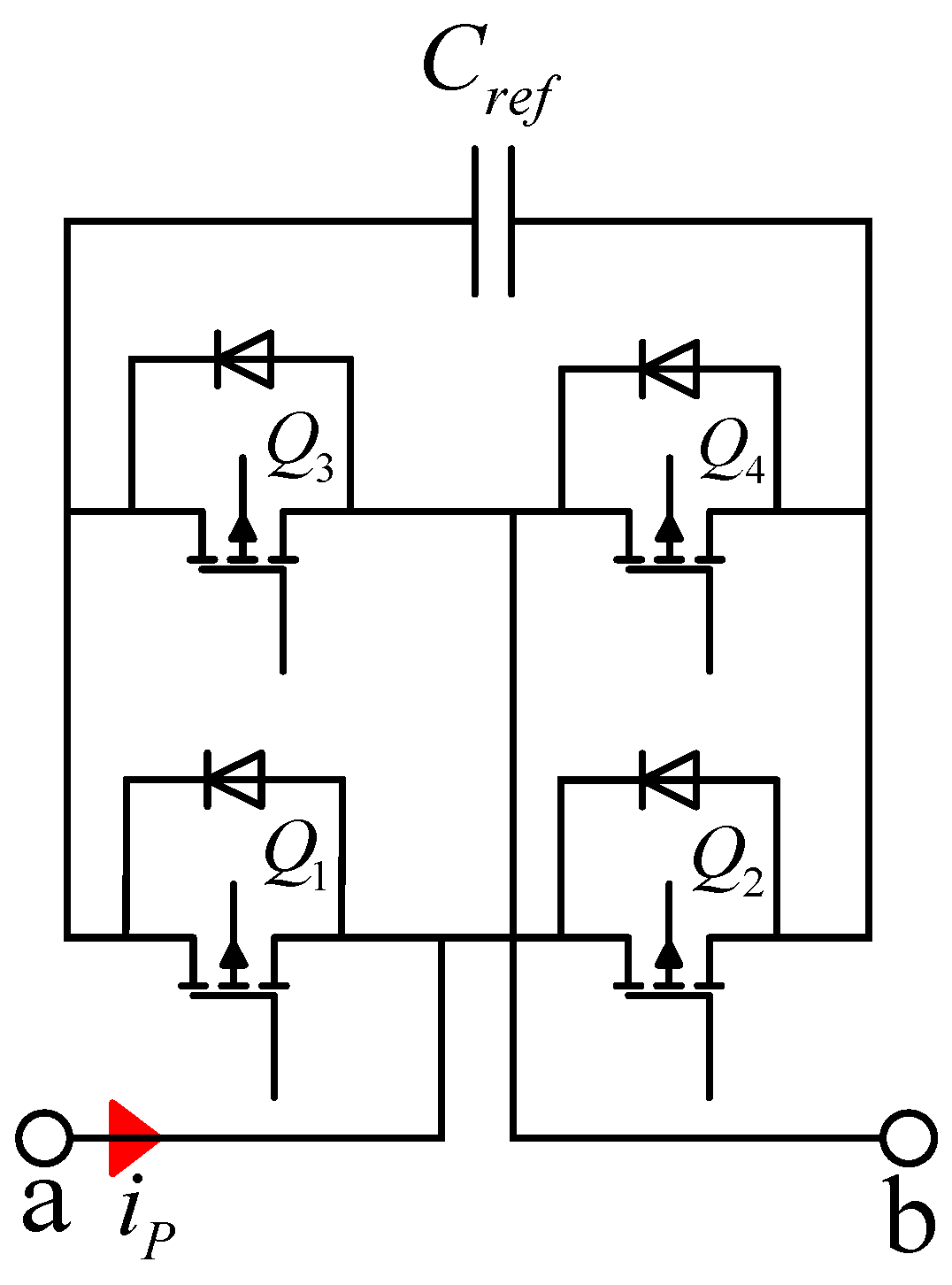
This section introduces the fundamental concepts of PCSI. And the placement of PCSI topology is determined according to the features of the LCC-S compensation network [20]. Then, the working principle of the proposed topology is discussed.

2.1. PCSI Topology

The proposed topology of the PCSI is shown in Figure 1. This topology consists of a parallel capacitor C r e f and four MOSFETs Q 1 ~ Q 4 . Depending on the system, this topology can be either capacitive or inductive through the interaction between MOSFETs and the capacitor C r e f , compensating for the missing reactance in the line during a system mismatch. Within this, the shunt capacitor C r e f works as an independent energy storage component, with the responsibility of storing and releasing energy to deal with line detuning [21]. So, its value is irrelevant and independent of the whole system. Once the resonant state changes, the circuit can automatically compensate for the missing reactance with a simple control.

2.2. PCSI Topology Position

In the WPT system, the initial consideration should be the selection of an appropriate location, as its placement is intricately linked to the overall system performance [22]. It is first necessary to analyze the characteristics of the LCC-S circuit, which can help determine where the location is best. Its system is shown in Figure 2, where L P is the compensation inductance. C 1 and C P are two compensation capacitors at the primary side. i L is the output current for the inverter. L 1 and L 2 are the primary coil and secondary coil. i P is the current flowing through the primary coil. R 0 is the load resistance. R 1 and R 2 are the parasitic resistance for Tx&Rx coils. Figure 3 illustrates the equivalent circuit diagram of LCC-S. U 1 is the voltage that passes through the inverter. Z s t is the equivalent impedance reflected from the receiving side. In order to ensure the whole system’s efficiency and power density on the receiving side, the PCSI topology is added to the primary side of the system.
The system resonance conditions are [19]
ω L P = 1 ω C P ω L 1 L P = 1 ω C 1 ω L 2 = 1 ω C 3
It can be seen from Figure 2 that the impedance of the receiving side of the system Z S is
Z S = R 2 + 1 j ω C 3 + j ω L 2 + 8 π 2 R 0
The equivalent impedance Z s t reflected from the receiving side to the transmitting side is
Z s t = j ω M I ˙ C I ˙ L = j ω M I ˙ L × j ω M I ˙ L Z S = ω M 2 Z S
The total input impedance Z i n on the transmitting side is
Z i n = R p + j ω L p + 1 j ω C p + 1 j ω L 1 + Z s t + 1 j ω C 1 + R 1
When the primary resonant capacitors changes, the resonant state of the system changes. Equation (1) becomes
j ω L P + 1 j ω C P 1 = a j ω L 1 j ω L P + 1 j ω C 11 = b j ω L 2 1 j ω C 3 = c
where a , b and c are the margins, then Equation (4) can be changed to
Z i n = R p + j ω L p + 1 1 a j ω L P + 1 a + b 1 j ω C P 1 1 j ω C 11 + R 1 + Z s t + 1 j ω C 1
Z s t is related to c . The loop current i L on the primary sides is
I ˙ L = U 1 Z i n
Due to the characteristics of PCSI topology, which can express inductive or capacitive, it could be linked to variable impedance. As shown in Figure 2, there are two potential positions within the LCC-S topology for placing the PCSI topology circuit. Based on the analysis of Equation (6), placing the PCSI topology at position ① only allows for tuning C P . However, when the topology of the circuit is placed at ②, the topology could tune C P , C 1 , and C 3 , which has a more substantial impact on the entire system. Consequently, the proposed circuit is chosen to be placed in ②, which helps tune the whole system. After adding the proposed topology, the complete system is shown in Figure 4.

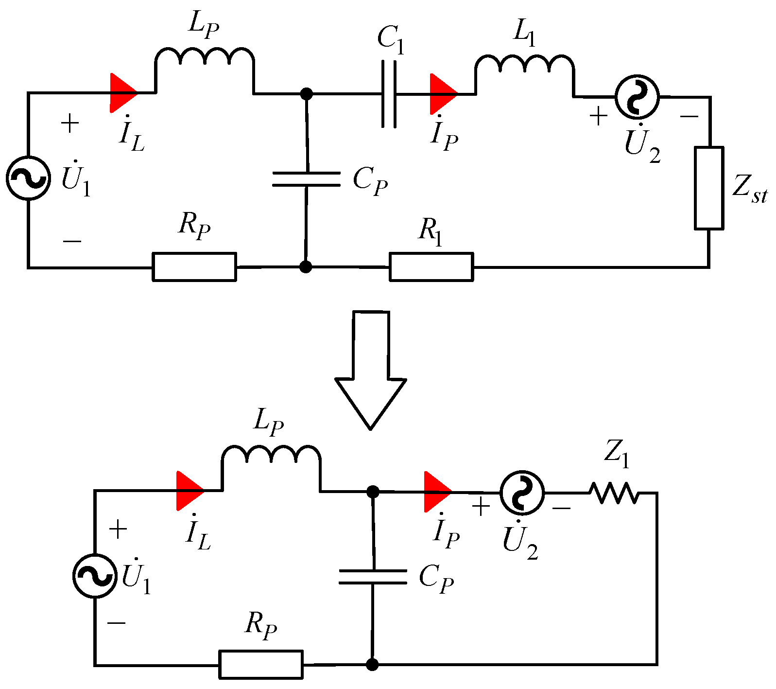
2.3. Principle of PCSI Operation

2.3.1. Working Principle of PCSI Topology

After ensuring the PCSI topology at a most suitable location in the previous section, assuming negligible power loss [23] in the PCSI upon its integration into the system, the proposed topology can be equated as an AC voltage source u 2 . This equivalent circuit is illustrated in Figure 5.
Z 1 = 1 j ω C 1 + j ω L 1 + Z s t + R 1 = R + j X
where Z 1 is the line equivalent impedance. According to Kirchhoff’s Voltage Law (KVL),
j ω L P + 1 j ω C P I ˙ L I ˙ P + I ˙ L R P = U ˙ 1
1 j ω C P I ˙ L I ˙ P I ˙ P R j I ˙ P X = U ˙ 2
It can be obtained from Equations (9) and (10),
I ˙ P = U ˙ 2 1 ω 2 L P C P + j ω C P R P U ˙ 1 A + j B
where A = ω 2 L P C P + ω C P R P X R P R 1 , B = ω 2 L P C P X C P R P R 1 X ω L P .
I ˙ P = U ˙ 2 1 ω 2 L P C P j ω C P R P U ˙ 1 A j B
The active power supplied by the PCSI topology is 0,
Re U ˙ 2 I ˙ P = U 2 cos β + j U 2 sin β × I ˙ P = 0
where β is the phase shift with respect to U ˙ 1 ,
U 2 = U 1 A cos β C U 1 B sin β C
where C = A ω 2 L P C P A + ω C P R P B .
Z i n = U ˙ 1 I ˙ L = C A A ω 2 L P C P B ω C P R P + j C ω C P R P ω 2 L P C P
where Z i n is the total impedance of the line.
Z 2 = U ˙ 2 I ˙ P = j C 4 A 2 cos 2 β A 2 + 3 B 2 4 B 2 sin 2 β j C ω C P R P ω 2 L P C P
where Z 2 is the equivalent impedance of the PCSI topology. Equation (16) shows that the excess reactance in the system can be canceled out when β = π 3   o r   2 π 3 .

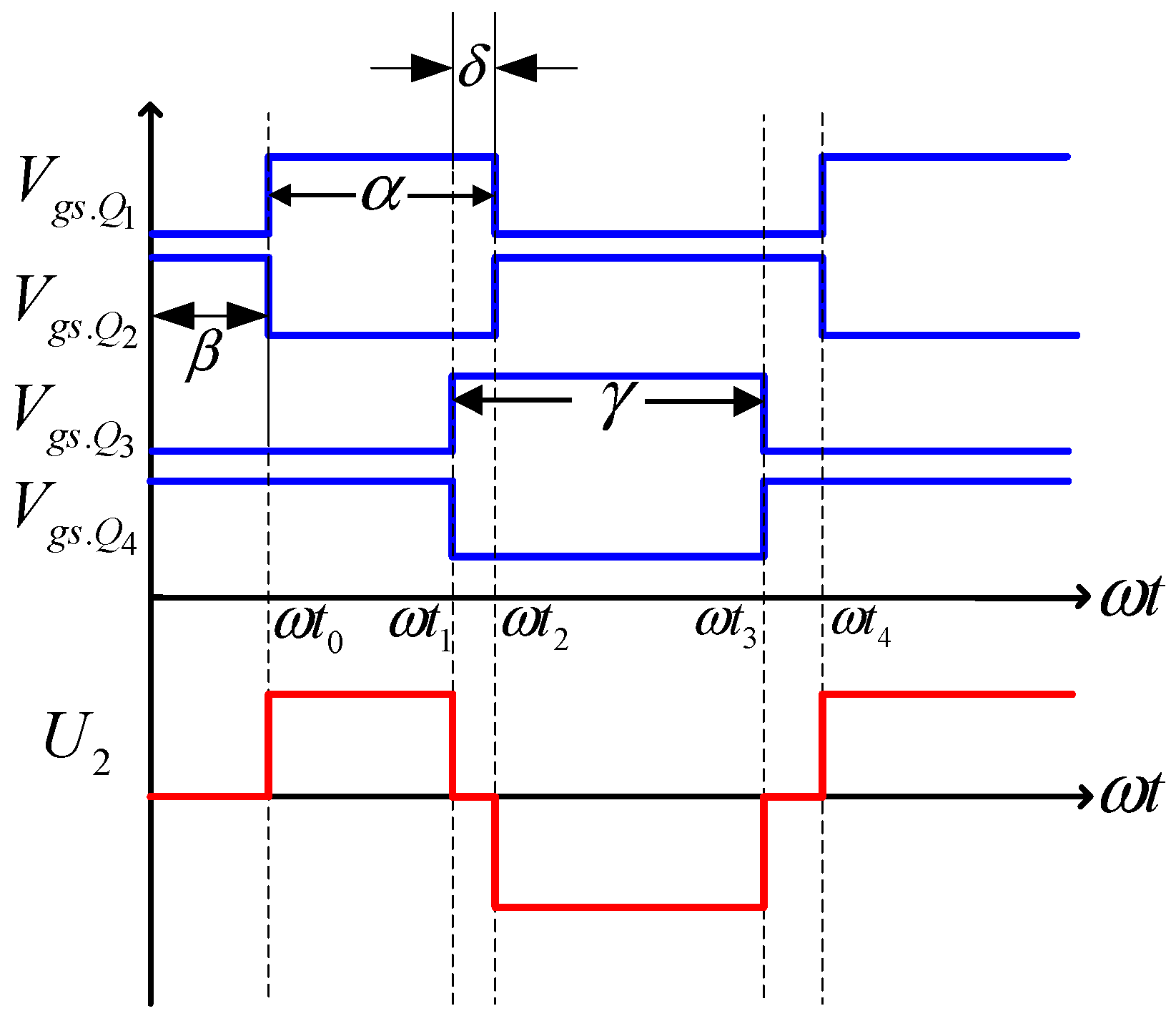
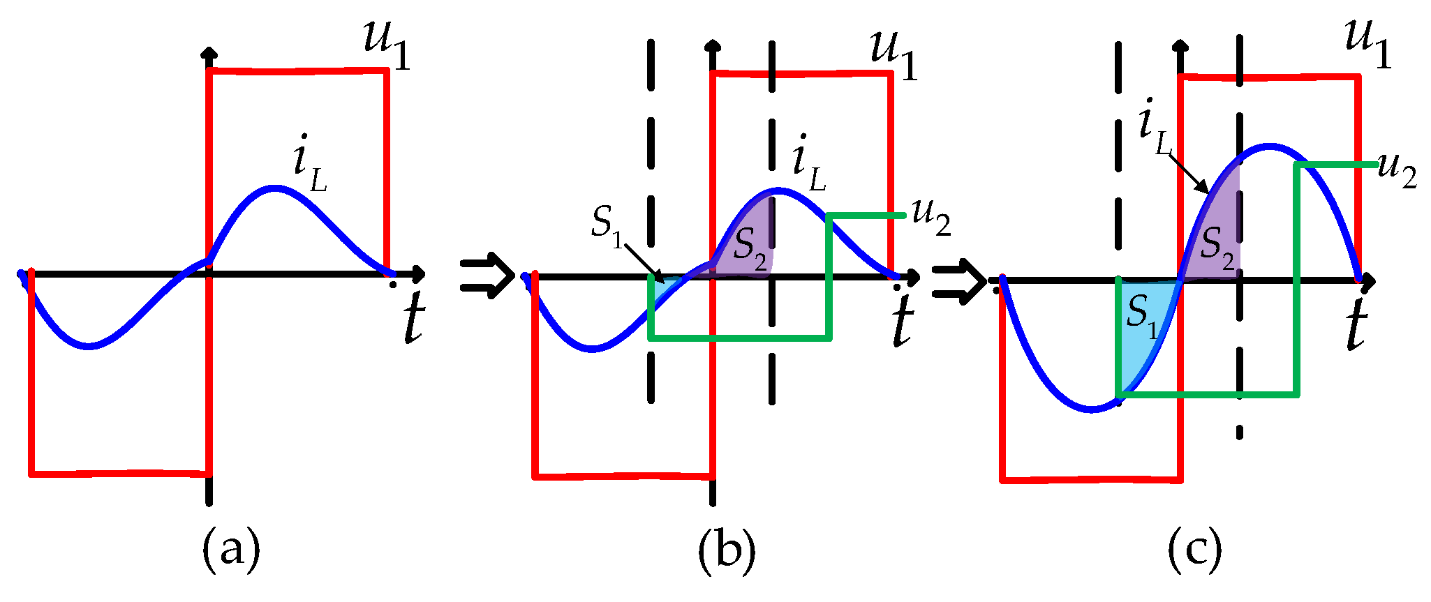
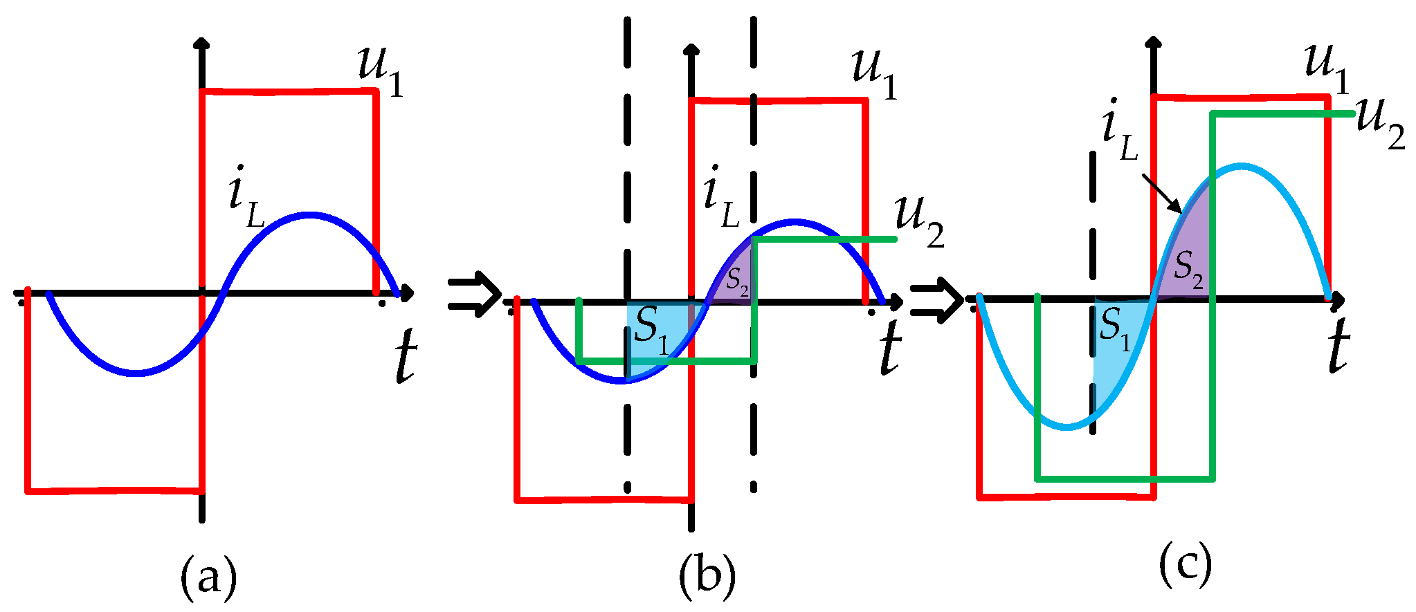
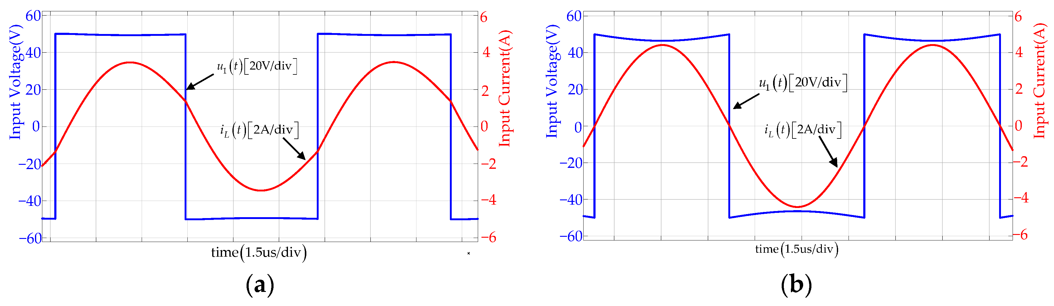
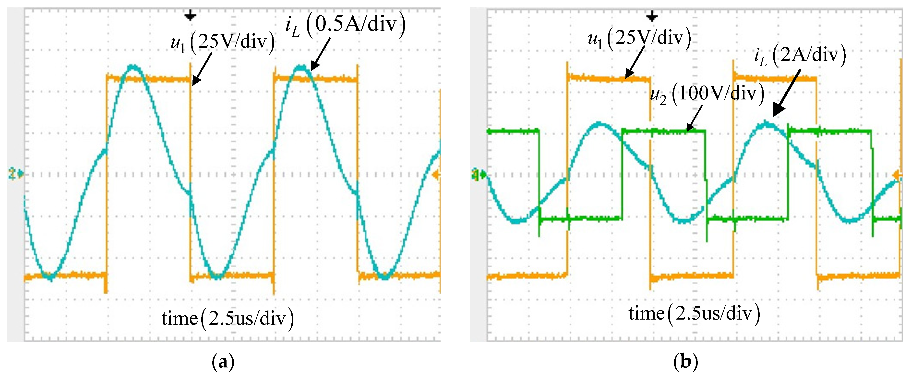
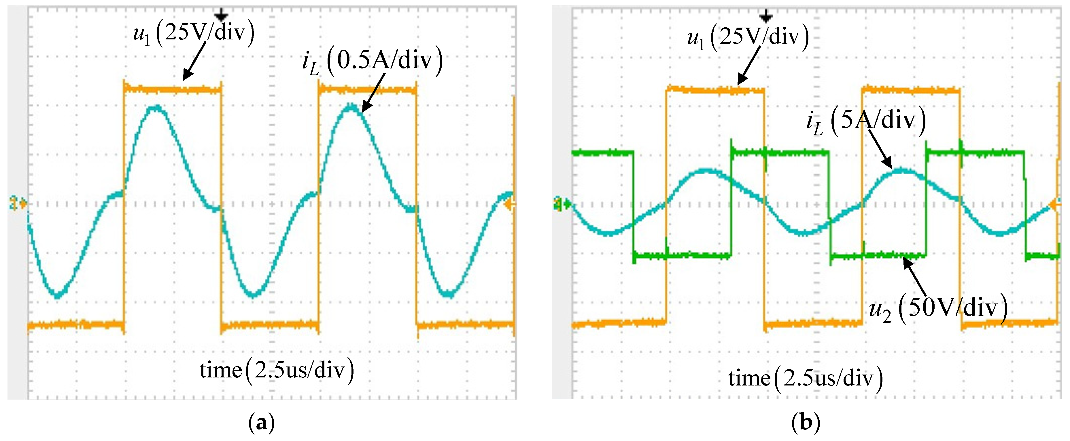
2.3.2. Waveforms of PCSI Topology

The waveform of the PCSI topology, as shown in Figure 6, can be derived based on the findings from the preceding section. Here, Q 1 represents the pulse signal with a duty cycle of α , while Q 3 denotes its complementary pulse signal Q 1 . Likewise, Q 2 signifies the pulse signal with a duty cycle of γ , and Q 4 stands for its complementary signal. U 2 stands the PCSI topology’s output voltage. Equation (17) represents the quantitative relationship among them.
ω t 0 = β ω t 1 = α + β δ ω t 2 = α + β ω t 3 = α + β + γ 2 δ ω t 4 = 2 π
β is the conclusion obtained in the previous section. α and γ are pulse signals with a 50% duty cycle, and δ takes the value of 0. According to Equation (16), the phase angle between the output voltage u 1 of the inverter and the output voltage u 2 of PCSI is π 3   o r   2 π 3 .

2.3.3. Tuning Principle of PCSI Topology

When the capacitances C P and C 1 change their values, as indicated in Equations (5) and (6), the input impedance Z i n will also undergo modification. Consequently, the system’s resonant network frequency deviates from the inverter’s switching frequency, leading to detuning [24]. When both the capacitance C P and C 1 are reduced, Figure 7a illustrates a phase discrepancy between the inverter output voltage and the primary side current. The current i L surpasses the voltage u 1 , indicating a capacitive system [25]. Subsequently, the PCSI circuit is incorporated into the system as shown in Figure 7b, u 2 is the initial voltage of the proposed topology. And adjusting the topology output voltage u 2 is different by 2 / 3 π to u 1 , which is consistent with the conclusion obtained above. Initially, even although the charging area S 2 is larger than the discharging area S 1 at first, the amplitude of u 1 will escalate. When the charging area S 2 is equal to the discharging area S 1 , the topology tuning is completed. The waveforms are shown in Figure 7c, where the primary side current i L is adjusted to align in phase with the inverter output voltage u 1 , and the amplitude of i L also enlarges due to the presence of C r e f .
Likewise, as depicted in Figure 8a. If the resonant capacitors’ values of system components C 1 and C P become excessive, they disrupt the resonant condition of the system, leading to a mismatch. At this time, the inverter output voltage u 1 of the system exceeds the primary side current i L , leading to indictive [26]. As shown in Figure 8b, the charging area S 2 is smaller than the discharging area S 1 consequently putting the PCSI’s output voltage at π / 3 , which differs to u 1 . The voltage of C r e f increases with the alterations of charging and discharging area, resulting in an elevation of the primary side current i L during the tuning process. Once the charging area S 2 equals the discharging area S 1 , the tuning process is over, and the result is depicted in Figure 8c. The current i L is in phase with the voltage u 1 , and its amplitude enlarges.

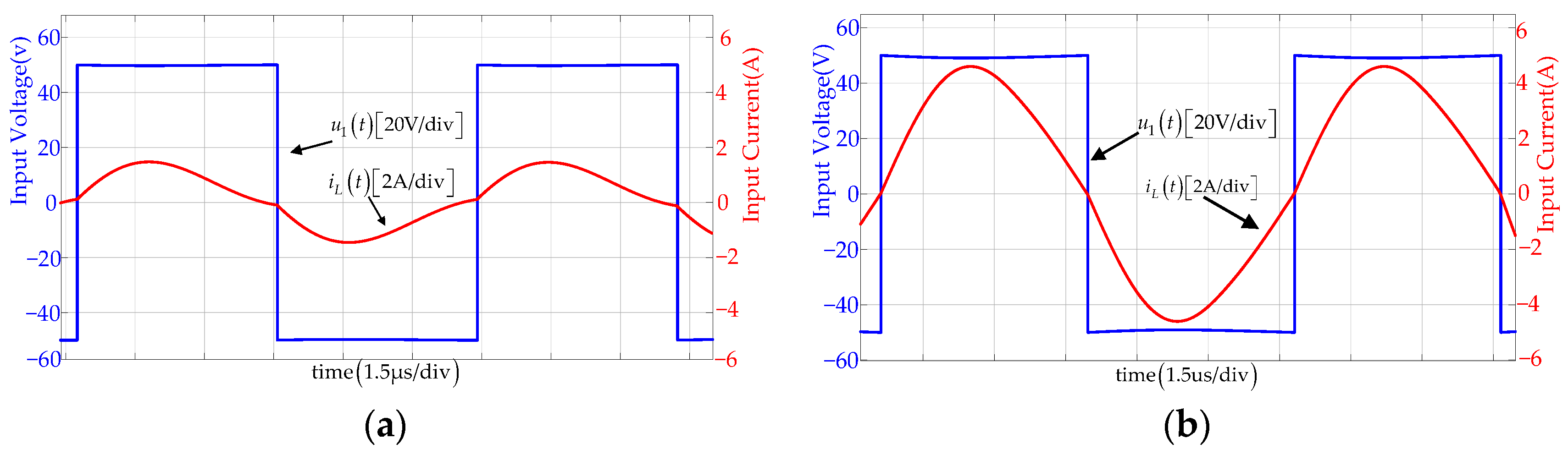
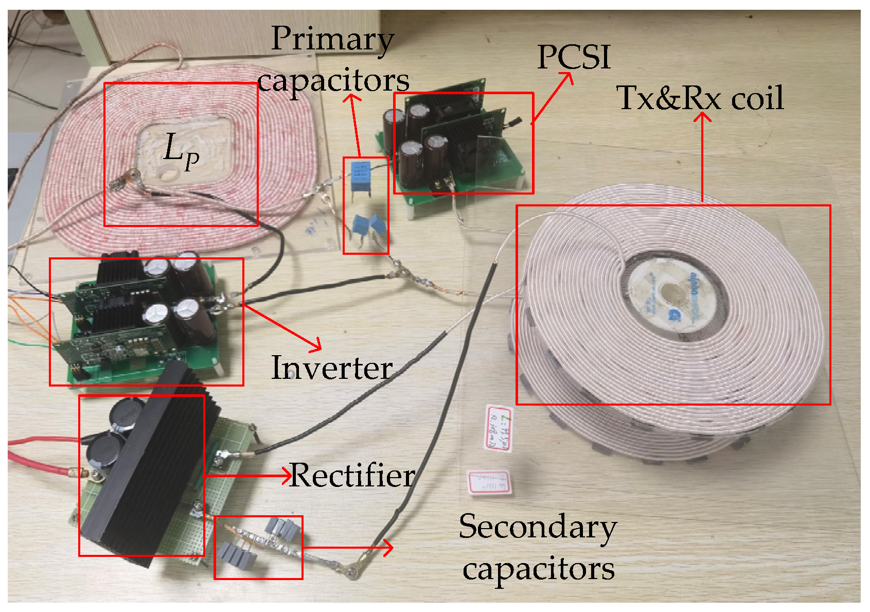
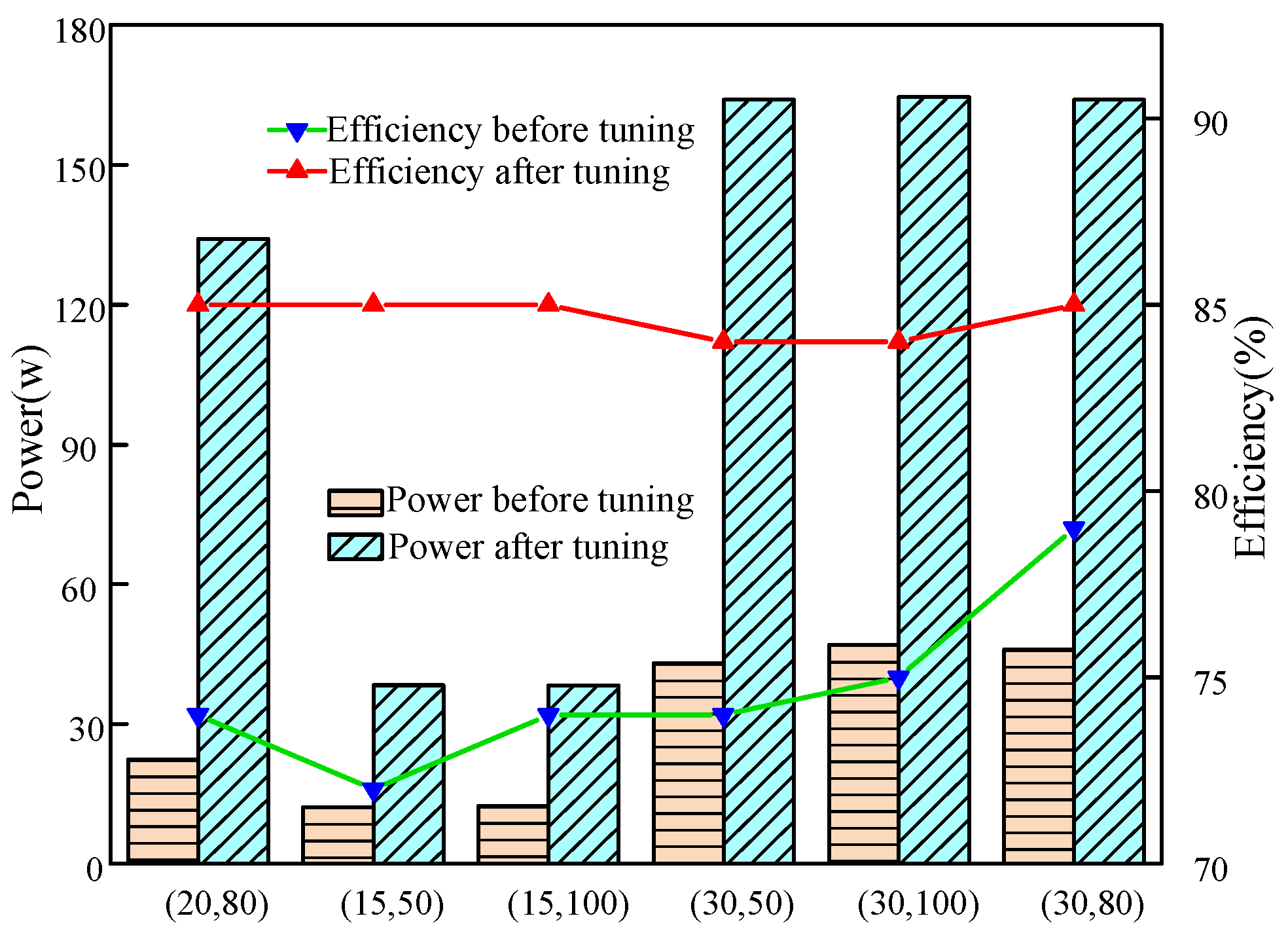
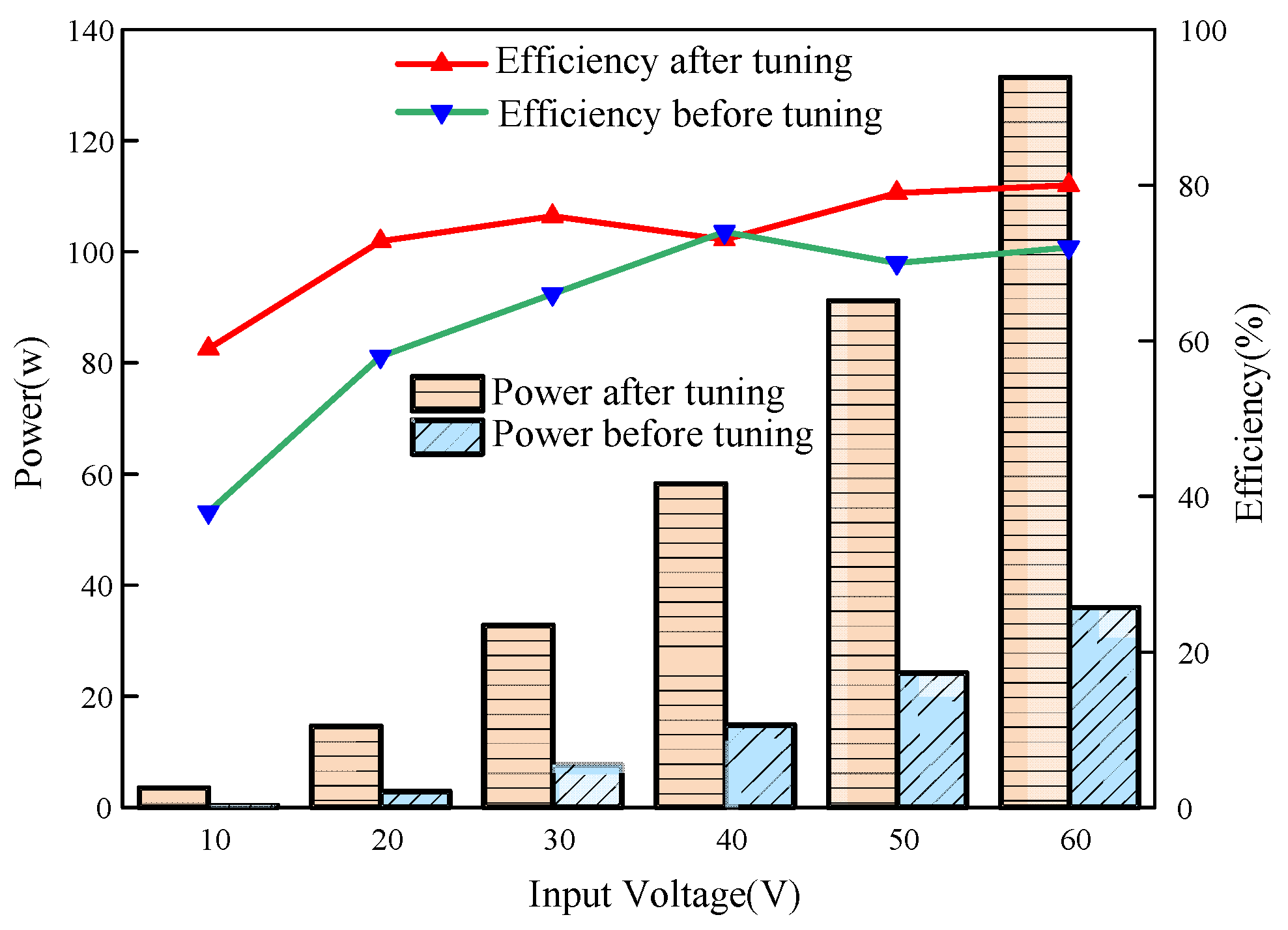
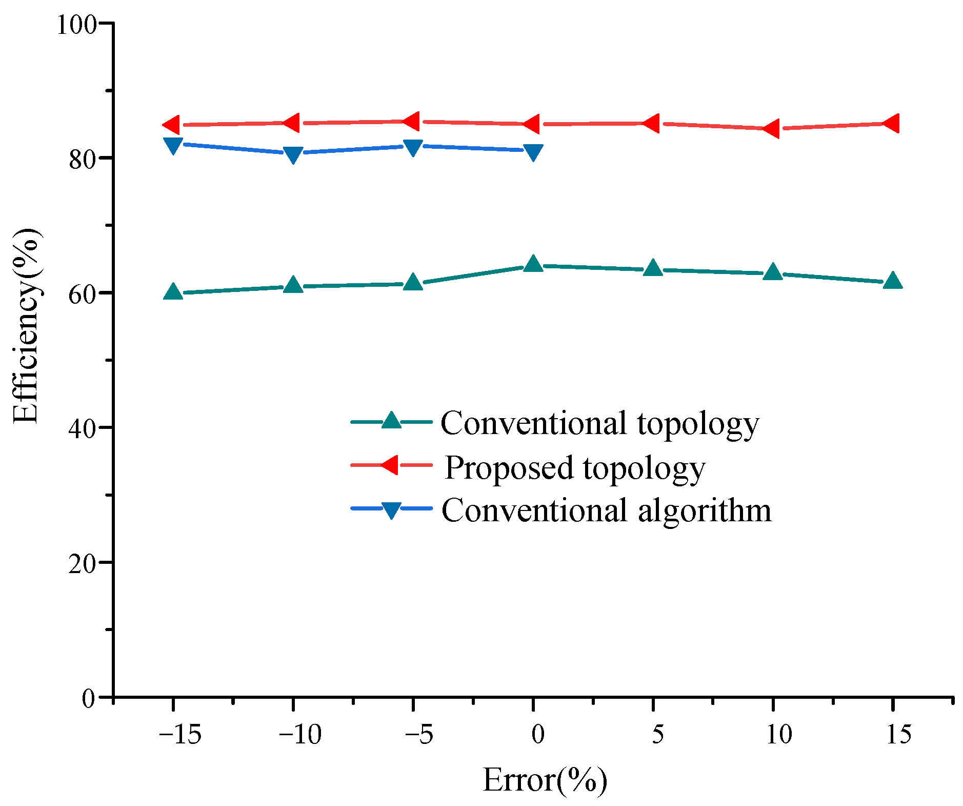
3. Result Simulation and Experimental Verification

In this section, the simulation model is firstly built on the MATLAB/Simulink platform. Its switching frequency is fixed at 100 kHz, and the inverter outputs a square wave signal with a pulse width of 50%. The PCSI topology output voltage phase should be 60 or 120 relative to the primary inverter, according to Equation (16). The detuned state is simulated by changing the values of the resonant capacitors C 1 and C P .
As shown in Figure 9a, when the values of the resonant capacitors decrease, the primary current i L exceeds the inverter’s output voltage u 1 and the system is capacitive. By incorporating the PCSI circuit topology and adjusting its phase, the waveforms are shown in Figure 9b. At this point, the voltage u 1 and current i L in this system are in phase.
The same phenomenon is illustrated in Figure 10a after augmenting the values of the resonant capacitors in the system. The inverter’s output voltage u 1 exceeds the primary current i L . Meanwhile, the system is inductive. Upon integrating the PCSI topology, the waveforms are shown in Figure 10b. The current i L increases, aligning the voltage u 1 in phase with it.
Both of the above simulations increase the amplitude of the current i L differently. And the detuning states of the system are changed due to the addition of PCSI topology.
The simulation results demonstrate the feasibility of the aforementioned theory. As shown in Figure 11, a principal prototype of the WPT system based on the LCC-S compensation network is built to demonstrate the proposed topology using the system parameters in Table 1. The MOSFETs (SPW55N85C3) were used in the inverter and the PCSI topology, and the resonant capacitors (B32922C3154M) were used in the compensation network during the whole experiment. The rectifier consists of diodes (RHRG5068). Both the primary and secondary sides of the Litz lines, which have 15 turns, have the same inner diameter of 40 mm, with a separation of 60 mm. The waveforms are recorded by a Tektronix oscilloscope (TDS2024C). The signals controlling the inverter and PCSI topology are generated by the same development board. A constant resistive load is used throughout the simulations and measurements. As noted in [15], the value of the resonant capacitance varies with the materials, with the negative drift being more prominent than the positive. Therefore, the value of the resonant capacitor is adjusted within the range of −40% to 20% throughout the experiments.
The following is the specific experiment process: Figure 12 shows the waveforms before and after the system tuning, and the resonant capacitors C P and C 1 are reduced. In Figure 12a, the switching frequency is not equal to the resonant frequency of the system. Consequently, the voltage u 1 is behind the current i L , indicating a capacitive system. In Figure 12b, the waveforms of the system are depicted after integrating the PCSI topology, which is adjusted by the PCSI to realize ZPA at the beginning of the whole duty. At the same time, the inverter output voltage u 1 and the primary side current i L are in phase.
Figure 13a shows a specific phase difference between u 1 and i L and that the system is capacitive. Figure 13b shows that by incorporating the PCSI topology to adjust the system, it can effectively eliminate the line mismatch phenomenon, resulting in voltage and current alignment. Meanwhile, the PCSI output voltage u 2 differs by π / 3 to u 1 .
Figure 14 and Figure 15 present the resonant capacitor C P with a fixed value, while sequentially altering the value of capacitor C 1 . In Figure 14a and Figure 15a, a phase difference between voltage u 1 and current i L is depicted. The voltage exceeds the current, and the primary side of the whole system appears inductive. The waveforms depicted in Figure 14b and Figure 15b illustrate that the PCSI circuit consistently compensates for line mismatch, even after modifying the value of C 1 . The phase difference between u 2 and u 1 is π / 3 .
To demonstrate the effectiveness of the PCSI topology, its performance is firstly evaluated for varying resonant capacitance drifts. Figure 16 illustrates the system’s output power and efficiency under different capacitor drifts while maintaining a constant input voltage. With the integration of the PCSI, the power of the system is increased by 40 W~150 W compared to the previous configuration. Additionally, the efficiency of the system is increased by 9~13% under the same conditions.
Figure 17 shows the power and efficiency of the system before and after tuning, achieved by adjusting the input voltages while maintaining the constant resonant capacitance value ( C P is 20 nf; C 1 is 50 nf). The results indicate that after adding the PCSI topology, the output power of the system is improved by 3W~100W in comparison with the previous configuration. Furthermore, the efficiency of the system is improved by 1~10% in the same case.
To validate the proposed topology’s effectiveness, we sequentially compare the efficiency of both the proposed topology and algorithm within the same resonant capacitance offset range. Within the LCC-S resonant network, the topology presented in this paper ensures a system efficiency of approximately 85%, surpassing that of the topology suggested in [19]. The proposed topology exhibits higher efficiency compared to the conventional algorithm [15], and its tuning range is significantly broader than that of the conventional algorithm. Figure 18 shows the performance of the proposed topology with regard to both efficiency and tuning range.

4. Conclusions

This paper introduces a PCSI line topology, which acts as a variable impedance in the line to compensate for excess reactance caused by detuning. It automatically adjusts detuning to keep the system in a stable state. MATLAB/Simulink simulations and the constructed system model demonstrate that, within a broad range of conditions (when the resonant capacitance is between −40% and 20% of the standard value), the primary voltage and current of the system can remain in phase even after integrating the PCSI topology.
To comprehensively validate the proposed topology’s performance, two distinct sets of experiments are sequentially employed for a comparative above analysis. Initially, the output voltage is constant, and the various values of resonant capacitors are utilized. Then, the power and efficiency of the entire WPT system are sequentially calculated, both before and after tuning. Subsequently, a specific set of resonant capacitor values is held constant, and varying input voltages are employed to compare the power and efficiency of the system, before and after tuning. The experiment results indicate that, in both scenarios, there is an increase in both power and efficiency to varying extents. This validates the performance enhancement of this topology for the entire system.
Furthermore, as the PCSI is a communication-less topology in the WPT system, which is not affected by other modules, the detuning system can be autonomously adjusted. This topology could remove complex control processes and enable for higher performance in the system because of its features. Similarly, the proposed topology is also suitable for poor conditions such as a low coupling factor, which provides direction for future work.

Author Contributions

Conceptualization, J.L.; methodology, B.M.; software, S.S.; validation, L.C. and J.L.; writing—original draft preparation, B.M.; writing—review and editing, J.L.; project administration, L.C.; funding acquisition, J.L. All authors have read and agreed to the published version of the manuscript.

Funding

This research was funded by the Hubei Provincial Education Department Scientific Research Program Funding Projects grant number [Q20211101].

Data Availability Statement

Data are contained within the article.

Conflicts of Interest

The authors declare no conflict of interest.

References

  1. Liang, M.; Khamlichi Drissi, K.E.; Pasquier, C. Optimal frequency for Dynamic Wireless Power Transfer. In Proceedings of the 2022 24th European Conference on Power Electronics and Applications (EPE’22 ECCE Europe), Hanover, Germany, 5–9 September 2022; pp. 1–10. [Google Scholar]
  2. Vailshery, L.S. Number of IoT Connected Devices Worldwide 2019–2021, with Forecasts to 2030. Available online: https://www.statista.com/statistics/1183457/iot-connected-devices-worldwide/ (accessed on 12 September 2023).
  3. Sinha, S.; Regensburger, B.; Kumar, A.; Afridi, K. A very-high-power-transfer-density GaN-based capacitive wireless power transfer system. In Proceedings of the 2017 IEEE 5th Workshop on Wide Bandgap Power Devices and Applications (WiPDA), Albuquerque, NM, USA, 30 October–1 November 2017; pp. 360–365. [Google Scholar]
  4. Li, S.; Liu, Z.; Zhao, H.; Zhu, L.; Shuai, C.; Chen, Z. Wireless Power Transfer by Electric Field Resonance and Its Application in Dynamic Charging. IEEE Trans. Ind. Electron. 2016, 63, 6602–6612. [Google Scholar] [CrossRef]
  5. Mahesh, A.; Chokkalingam, B.; Mihet-Popa, L. Inductive Wireless Power Transfer Charging for Electric Vehicles—A Review. IEEE Access 2021, 9, 137667–137713. [Google Scholar] [CrossRef]
  6. Gu, L.; Rivas-Davila, J. 1.7 kW 6.78 MHz Wireless Power Transfer with Air-Core Coils at 95.7% DC-DC Efficiency. In Proceedings of the 2021 IEEE Wireless Power Transfer Conference (WPTC), San Diego, CA, USA, 1–4 June 2021; pp. 1–4. [Google Scholar]
  7. Peng, P.; Zhou, W.; Li, L.; He, J.B.; Peng, B.; Yu, H.J.; He, X.P. Drift of MEMS Capacitive Accelerometers for One-Year Room-Temperature Storage: A Simulation and Experimental Study. IEEE Sens. J. 2023, 23, 202–210. [Google Scholar] [CrossRef]
  8. Lim, Y.S.; Tang, H.Y.; Lim, S.; Park, J.S. An Adaptive Impedance-Matching Network Based on a Novel Capacitor Matrix for Wireless Power Transfer. IEEE Trans. Power Electron. 2014, 29, 4403–4413. [Google Scholar] [CrossRef]
  9. Zhao, J.; Zhang, J.Z.; Zhu, Y.D. A Flexible Wireless Power Transfer System With Switch Controlled Capacitor. IEEE Access 2019, 7, 106873–106881. [Google Scholar] [CrossRef]
  10. Zhang, J.Z.; Zhao, J.; Zhang, Y.Q.; Deng, F.J. A Wireless Power Transfer System With Dual Switch-Controlled Capacitors for Efficiency Optimization. IEEE Trans. Power Electron. 2019, 35, 6091–6101. [Google Scholar] [CrossRef]
  11. Wang, X.Q.; Xu, J.P.; Ma, H.B.; He, S.Z. Inductive Power Transfer Systems With Digital Switch-Controlled Capacitor for Maximum Efficiency Point Tracking. IEEE Trans. Ind. Electron. 2021, 68, 9467–9480. [Google Scholar] [CrossRef]
  12. Luo, Z.C.; Zhao, Y.Y.; Xiong, M.; Wei, X.Z.; Dai, H.F. A Self-Tuning LCC/LCC System Based on Switch-Controlled Capacitors for Constant-Power Wireless Electric Vehicle Charging. IEEE Trans. Ind. Electron. 2022, 70, 709–720. [Google Scholar] [CrossRef]
  13. Sinha, S.; Regensburger, B.; Kumar, A.; Afridi, K. A Multi-MHz Large Air-gap Capacitive Wireless Power Transfer System Utilizing an Active Variable Reactance Rectifier Suitable for Dynamic Electric Vehicle Charging. In Proceedings of the 2019 IEEE Energy Conversion Congress and Exposition (ECCE), Baltimore, MD, USA, 29 September–3 October 2019; pp. 5726–5732. [Google Scholar]
  14. Maji, S.; Etta, D.; Afridi, K. A High-Power Large Air-Gap Multi-MHz Dynamic Capacitive Wireless Power Transfer System Utilizing an Active Variable Reactance Rectifier for EV Charging. In Proceedings of the 2022 IEEE Energy Conversion Congress and Exposition (ECCE), Detroit, MI, USA, 9–13 October 2022; pp. 1–6. [Google Scholar]
  15. Song, K.; Yang, G.; Zhang, H.; Huang, X.L.; Jiang, J.H.; Lan, Y.; Huang, X.H.; Li, J.; ZHU, C.B. An Impedance Decoupling-Based Tuning Scheme for Wireless Power Transfer System Under Dual-Side Capacitance Drift. IEEE Trans. Power Electron. 2021, 36, 7526–7536. [Google Scholar] [CrossRef]
  16. Ishihara, M.; Matsuura, K.; Konishi, A.; Umetani, K.; Hiraki, E. Cross-Interference Free 6.78 MHz Multiple-Transmitter Using Power Factor Based Control for Wide-Area Wireless Power Transfer Systems. In Proceedings of the 2022 IEEE Energy Conversion Congress and Exposition (ECCE), Detroit, MI, USA, 9–13 October 2022; pp. 1–7. [Google Scholar]
  17. Endo, Y.; Furukawa, Y. Proposal for a new resonance adjustment method in magnetically coupled resonance type wireless power transmission. In Proceedings of the 2012 IEEE MTT-S International Microwave Workshop Series on Innovative Wireless Power Transmission: Technologies, Systems, and Applications, Kyoto, Japan, 10–11 May 2012; pp. 263–266. [Google Scholar]
  18. Mastuura, K.; Narusue, Y.; Morikawa, H. Magnetic field intensity suppression using communication-less impedance adjust-ment for inductive power transfer systems. IEICE Electron. Exp. 2023, 20, 20230153. [Google Scholar]
  19. Mastuura, K.; Kobuchi, D.; Narusue, Y.; Morikawa, H. Communication-Less Receiver-Side Resonant Frequency Tuning for Magnetically Coupled Wireless Power Transfer Systems. IEEE Access 2023, 11, 23544–23556. [Google Scholar]
  20. Shi, L.X.; Alou, P.; Oliver, J.A.; Rodriguez, J.C.; Delgado, A.; Cobos, J.A. A Self-Adaptive Wireless Power Transfer System to Cancel the Reactance. IEEE Trans. Ind. Electron. 2020, 68, 12141–12151. [Google Scholar] [CrossRef]
  21. Sinha, S.; Kumar, A.; Regensburger, B.; Afridi, K.K. A New Design Approach to Mitigating the Effect of Parasitics in Capacitive Wireless Power Transfer Systems for Electric Vehicle Charging. IEEE Trans. Transp. Electrif. 2019, 5, 1040–1059. [Google Scholar] [CrossRef]
  22. Shi, L.X.; Alou, P.; Oliver, J.A.; Cobos, J.A. A Novel Self-adaptive Wireless Power Transfer System to Cancel the Reactance of the Series Resonant Tank and Deliver More Power. In Proceedings of the 2019 IEEE Energy Conversion Congress and Exposition (ECCE), Baltimore, MD, USA, 29 September–3 October 2019; pp. 4207–4211. [Google Scholar]
  23. Lee, W.C.; Ahn, D. Wireless Power Transfer under Wide Distance Variation Using Dual Impedance Frequency. Electronics 2020, 9, 110. [Google Scholar] [CrossRef]
  24. Hu, H.S.; Cai, T.; Duan, S.X.; Zhang, X.M.; Niu, J.T.; Feng, H. An Optimal Variable Frequency Phase Shift Control Strategy for ZVS Operation Within Wide Power Range in IPT Systems. IEEE Trans. Power Electron. 2019, 35, 5517–5530. [Google Scholar] [CrossRef]
  25. Ahn, D.; Hong, S.C. Wireless Power Transmission with Self-Regulated Output Voltage for Biomedical Implant. IEEE Trans. Transp. Electrif. 2014, 61, 2225–2235. [Google Scholar] [CrossRef]
  26. Huang, Z.C.; Lam, C.S.; Mak, P.I.; Martins, R.P.; Wong, S.C.; Tse, C.K. A Single-Stage Inductive-Power-Transfer Converter for Constant-Power and Maximum-Efficiency Battery Charging. IEEE Trans. Power Electron. 2020, 35, 8973–8984. [Google Scholar] [CrossRef]
Figure 1. Topology of PCSI circuits.
Energies 16 08103 g001
Figure 2. LCC-S system.
Energies 16 08103 g002
Figure 3. Equivalent circuit of LCC-S.
Energies 16 08103 g003
Figure 4. LCC-S system with PCSI topology.
Energies 16 08103 g004
Figure 5. Equivalent circuit after adding PCSI circuit.
Energies 16 08103 g005
Figure 6. Voltage waveform of PCSI topology.
Energies 16 08103 g006
Figure 7. Resonance self-tuning process when the system is capacitive: (a) before tuning, (b) tuning process after adding PCSI topology and (c) after tuning.
Energies 16 08103 g007
Figure 8. Resonance self-tuning process when the system is inductive: (a) before tuning, (b) tuning process after adding PCSI topology and (c) after tuning.
Energies 16 08103 g008
Figure 9. Comparison of voltage and current before and after tuning: (a) main waveforms are reduced by C 1 and C P . (b) main waveforms after adding PCSI topology.
Energies 16 08103 g009
Figure 10. Comparison of voltage and current before and after tuning: (a) main waveforms are increased by C 1 and C P . (b) main waveforms after adding PCSI topology.
Energies 16 08103 g010
Figure 11. System model.
Energies 16 08103 g011
Figure 12. Main waveforms for C P = 20   nF , C 1 = 50   nF . (a) before. (b) after.
Energies 16 08103 g012
Figure 13. Main waveforms for C P = 15   nF , C 1 = 100   nF . (a) before. (b) after.
Energies 16 08103 g013
Figure 14. Main waveforms for C P = 30   nF , C 1 = 50   nF . (a) before. (b) after.
Energies 16 08103 g014
Figure 15. Main waveforms for C P = 30   nF , C 1 = 100   nF . (a) before. (b) after.
Energies 16 08103 g015
Figure 16. Comparison of system output power and efficiency under different capacitance drifts.
Energies 16 08103 g016
Figure 17. Comparison of system output power and efficiency under different input voltages.
Energies 16 08103 g017
Figure 18. Comparison of system efficiency under different techniques.
Energies 16 08103 g018
Table 1. System parameters.
ParametersValuesUnit
Input voltage U 0 60V
Inductance L P 100 μ H
Resistance of L P 0.5 Ω
Capacitor C 1 80 n F
Capacitor C 3 20 n F
Capacitor C P 25 n F
Coupling factor k 0.3
Primary inductance L 1 132 μ H
Secondary inductance L 2 132 μ H
Mutual inductance M 44 μ H
Resistance of TX&RX coils0.4 Ω
Load R 0 5 Ω
Disclaimer/Publisher’s Note: The statements, opinions and data contained in all publications are solely those of the individual author(s) and contributor(s) and not of MDPI and/or the editor(s). MDPI and/or the editor(s) disclaim responsibility for any injury to people or property resulting from any ideas, methods, instructions or products referred to in the content.

